Ion implantation into GaN -...
57
Ion implantation into GaN S.O. Kucheyev a,* , J.S. Williams a , S.J. Pearton b a Department of Electronic Materials Engineering, Research School of Physical Sciences and Engineering, The Australian National University, Canberra, ACT 0200, Australia b Department of Materials Science and Engineering, University of Florida, Gainesville, FL 32611, USA Accepted 18 January 2001 Abstract The current status of ion beam processing of GaN is reviewed. In particular, we discuss the following aspects of ion implantation into GaN: (i) damage build-up and amorphization, (ii) preferential surface disordering and loss of nitrogen during ion bombardment, (iii) ion-beam-induced porosity of amorphous GaN due to material dissociation, (iv) anomalous surface erosion during ion bombardment at elevated temperatures, (v) the effect of implantation disorder on mechanical properties, (vi) current progress on annealing of implantation disorder, (vii) electrical and optical doping, and (viii) electrical isolation. Emphasis is given to current problems which may hinder a successful application of ion implantation in the fabrication of GaN-based devices. # 2001 Elsevier Science B.V. All rights reserved. Keywords: GaN; Ion implantation; Implantation disorder; Annealing 1. Introduction For much of the past decade, GaN has been a subject of extensive research due to very important technological applications of this material. As is well documented in the literature [1], current applications of GaN include light-emitting diodes (LEDs), laser diodes, UV detectors, and microwave power and ultra-high power switches. In the fabrication of such GaN-based devices, ion bombardment represents a very attractive tool for several technological steps, such as electrical and optical selective-area doping, dry etching, electrical isolation, quantum well intermixing, and ion- cut. It is well-known that a successful application of ion implantation depends on understanding the production and annealing of radiation damage. Thus, detailed studies of ion implantation damage in GaN are not only important for investigating fundamental defect processes in solids under ion bombardment but are also essential for the fast developing GaN industry. Up to now, several outstanding reviews have appeared in the literature addressing various aspects of ion implantation into GaN [1–4]. However, very recently, the field of ion implantation into GaN has matured considerably. This review mainly concentrates on the recent progress made in the understanding of ion beam processes in GaN, which has not been reviewed previously. Sections 2–4 treat the structural characteristics of GaN exposed to ion bombardment. The mechanical properties of as-grown and ion implanted GaN are discussed in Section 5. In Section 6, we briefly discuss the Materials Science and Engineering, 33 (2001) 51–107 0927-796X/01/$ – see front matter # 2001 Elsevier Science B.V. All rights reserved. PII:S0927-796X(01)00028-6 * Corresponding author. Tel.: 61-2-61250464; fax: 61-2-61250511. E-mail address: [email protected] (S.O. Kucheyev).
Transcript of Ion implantation into GaN -...

Ion implantation into GaN
S.O. Kucheyeva,*, J.S. Williamsa, S.J. Peartonb
aDepartment of Electronic Materials Engineering, Research School of Physical Sciences and Engineering, The Australian
National University, Canberra, ACT 0200, AustraliabDepartment of Materials Science and Engineering, University of Florida, Gainesville, FL 32611, USA
Accepted 18 January 2001
Abstract
The current status of ion beam processing of GaN is reviewed. In particular, we discuss the following aspectsof ion implantation into GaN: (i) damage build-up and amorphization, (ii) preferential surface disordering and lossof nitrogen during ion bombardment, (iii) ion-beam-induced porosity of amorphous GaN due to materialdissociation, (iv) anomalous surface erosion during ion bombardment at elevated temperatures, (v) the effect ofimplantation disorder on mechanical properties, (vi) current progress on annealing of implantation disorder, (vii)electrical and optical doping, and (viii) electrical isolation. Emphasis is given to current problems which may hindera successful application of ion implantation in the fabrication of GaN-based devices. # 2001 Elsevier Science B.V.All rights reserved.
Keywords: GaN; Ion implantation; Implantation disorder; Annealing
1. Introduction
For much of the past decade, GaN has been a subject of extensive research due to very importanttechnological applications of this material. As is well documented in the literature [1], currentapplications of GaN include light-emitting diodes (LEDs), laser diodes, UV detectors, andmicrowave power and ultra-high power switches. In the fabrication of such GaN-based devices, ionbombardment represents a very attractive tool for several technological steps, such as electrical andoptical selective-area doping, dry etching, electrical isolation, quantum well intermixing, and ion-cut. It is well-known that a successful application of ion implantation depends on understanding theproduction and annealing of radiation damage. Thus, detailed studies of ion implantation damage inGaN are not only important for investigating fundamental defect processes in solids under ionbombardment but are also essential for the fast developing GaN industry.
Up to now, several outstanding reviews have appeared in the literature addressing variousaspects of ion implantation into GaN [1±4]. However, very recently, the field of ion implantation intoGaN has matured considerably. This review mainly concentrates on the recent progress made in theunderstanding of ion beam processes in GaN, which has not been reviewed previously. Sections 2±4treat the structural characteristics of GaN exposed to ion bombardment. The mechanical propertiesof as-grown and ion implanted GaN are discussed in Section 5. In Section 6, we briefly discuss the
Materials Science and Engineering, 33 (2001) 51±107
0927-796X/01/$ ± see front matter # 2001 Elsevier Science B.V. All rights reserved.
PII: S 0 9 2 7 - 7 9 6 X ( 0 1 ) 0 0 0 2 8 - 6
* Corresponding author. Tel.: �61-2-61250464; fax: �61-2-61250511.
E-mail address: [email protected] (S.O. Kucheyev).
current progress on the annealing of implantation damage. Sections 7 and 8 address the optical andelectrical characteristics, respectively. Applications of ion implantation in the fabrication of GaN-based electronic devices are discussed in Section 9. Finally, in Section 10, we summarize the currentproblems of ion beam processing of GaN which may limit the applications of ion implantation forthe fabrication of GaN-based devices.
A comment should be made about what is not included in detail in this review. We only brieflydiscuss the lattice sites of dopants implanted into GaN, studies of specific defect levels by deep leveltransient spectroscopy (DLTS), and studies of lattice disorder produced by dry etching (a recentreview on this topic can be found in [6]). Some of these studies have been reviewed in [1,5]. For thesame reason, we omit the discussion of rare-earth doping of GaN by ion implantation as well as theeffects of hydrogen implanted into GaN (see [1,5] for details on these topics). In addition, potentialapplications of ion implantation for ion-cut and quantum well intermixing in GaN are also onlybriefly mentioned here due to the lack of published literature on these subjects.
2. Damage build-up
Lattice disorder is always a concomitant effect of ion bombardment. Undesirable damageproduced by an ion beam is, in fact, the main problem for satisfactory electrical and optical dopingmade by ion implantation. Dry etching is also always accompanied by undesirable damageintroduced into near-surface layers. Therefore, studies of implantation disorder and its consequencesare necessary for a successful application of ion implantation in device fabrication. In this section,we discuss damage build-up in wurtzite GaN under ion bombardment.
2.1. Atomic displacements versus stable lattice damage
Given the current understanding of ion±solid interactions (see, for example, [7]), an energeticion penetrating through a GaN crystal generates a collision cascade which consists of vacancies inthe gallium and nitrogen sublattices (VGa and VN), gallium and nitrogen interstitials (Gai and Ni) [1],and, presumably, an amorphous zone in the cascade core in the case of heavy ions.1 Such acompletely disordered or amorphous zone is expected to form (but may not be stable) when thedamage level (and/or the energy deposited) in the collision (sub)cascade volume exceeds somethreshold value [8±10].
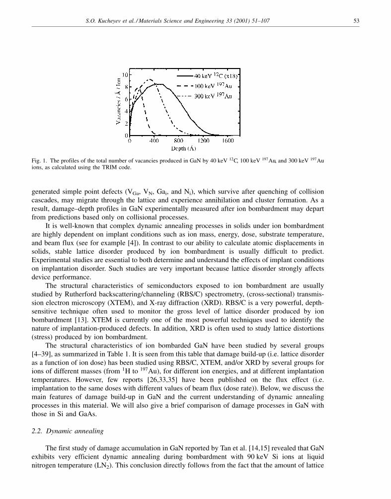
Ion ranges and atomic displacements produced in GaN by ion bombardment can be calculatedusing, for example, the TRIM code [11], a Monte Carlo computer simulation program. Othermethods often used to calculate the profiles of implanted species and atoms displaced involveanalytical calculations such as developed by Lindhard, Scharf, and Schiott (often called the LSStheory [7]) and an approach based on the Boltzmann transport equation [12]. For example, Fig. 1shows profiles of vacancies produced in GaN by implantation with 40 keV 12C, 100 keV 197Au, and300 keV 197Au ions, as calculated using the TRIM code [11]. It is seen from this figure that ionimplantation produces Gaussian-like (uni-modal) profiles of atomic displacements. The thickness ofthe layer modified by ion bombardment as well as the number of atomic displacements generateddepends on ion mass and energy, as illustrated in Fig. 1.
Such theoretical calculations of atomic displacements take into account only ballistic processesand completely neglect dynamic annealing (i.e. defect interaction processes). However, ion-
1 Here, we do not distinguish between interstitials of different symmetry.
52 S.O. Kucheyev et al. / Materials Science and Engineering 33 (2001) 51±107
generated simple point defects (VGa, VN, Gai, and Ni), which survive after quenching of collisioncascades, may migrate through the lattice and experience annihilation and cluster formation. As aresult, damage±depth profiles in GaN experimentally measured after ion bombardment may departfrom predictions based only on collisional processes.
It is well-known that complex dynamic annealing processes in solids under ion bombardmentare highly dependent on implant conditions such as ion mass, energy, dose, substrate temperature,and beam flux (see for example [4]). In contrast to our ability to calculate atomic displacements insolids, stable lattice disorder produced by ion bombardment is usually difficult to predict.Experimental studies are essential to both determine and understand the effects of implant conditionson implantation disorder. Such studies are very important because lattice disorder strongly affectsdevice performance.
The structural characteristics of semiconductors exposed to ion bombardment are usuallystudied by Rutherford backscattering/channeling (RBS/C) spectrometry, (cross-sectional) transmis-sion electron microscopy (XTEM), and X-ray diffraction (XRD). RBS/C is a very powerful, depth-sensitive technique often used to monitor the gross level of lattice disorder produced by ionbombardment [13]. XTEM is currently one of the most powerful techniques used to identify thenature of implantation-produced defects. In addition, XRD is often used to study lattice distortions(stress) produced by ion bombardment.
The structural characteristics of ion bombarded GaN have been studied by several groups[4±39], as summarized in Table 1. It is seen from this table that damage build-up (i.e. lattice disorderas a function of ion dose) has been studied using RBS/C, XTEM, and/or XRD by several groups forions of different masses (from 1H to 197Au), for different ion energies, and at different implantationtemperatures. However, few reports [26,33,35] have been published on the flux effect (i.e.implantation to the same doses with different values of beam flux (dose rate)). Below, we discuss themain features of damage build-up in GaN and the current understanding of dynamic annealingprocesses in this material. We will also give a brief comparison of damage processes in GaN withthose in Si and GaAs.
2.2. Dynamic annealing
The first study of damage accumulation in GaN reported by Tan et al. [14,15] revealed that GaNexhibits very efficient dynamic annealing during bombardment with 90 keV Si ions at liquidnitrogen temperature (LN2). This conclusion directly follows from the fact that the amount of lattice
Fig. 1. The profiles of the total number of vacancies produced in GaN by 40 keV 12C, 100 keV 197Au, and 300 keV 197Auions, as calculated using the TRIM code.
S.O. Kucheyev et al. / Materials Science and Engineering 33 (2001) 51±107 53

disorder measured experimentally is much less than that predicted by ballistic calculations (such asthe TRIM code [11]), which take into account only collisional processes and neglect defect diffusionand annihilation. Further studies of damage processes in GaN [16±37,39] have confirmed thepresence of very efficient dynamic annealing in GaN under a wide range of implant conditions (seeTable 1). These studies [16±37,39] have also revealed a number of other interesting features ofdamage build-up in GaN under ion bombardment, which will be discussed below.
First of all, strong dynamic annealing in GaN results in a somewhat unexpected damage build-up behavior with increasing ion dose. For example, shown in Fig. 2 are RBS/C spectra illustratingdamage accumulation in GaN with dose for 300 keV Au ions implanted at LN2 with a beam flux of3:1� 1012 cmÿ2 sÿ1 (Fig. 2(a)) and at room temperature (RT) with a beam flux of4:4� 1012 cmÿ2 sÿ1 (Fig. 2(b)). A comparison of Fig. 2(a) and (b) reveals quite different damagebuild-up behavior with increasing dose of 300 keV Au ions for LN2 and RT bombardment regimes.Indeed, for LN2 irradiation, for doses up to �2� 1014 cmÿ2, Fig. 2(a) shows accumulation ofdamage preferentially at the GaN surface, away from the maximum of the nuclear energy loss profile(see Fig. 1). Then, in a narrow dose range from �2� 1014 to �3� 1014 cmÿ2, damage in the GaNbulk region (�500 AÊ from the GaN surface) exhibits a very rapid increase from a very low level tocomplete disordering (i.e. to amorphization), as indicated by the RBS/C yield reaching the randomlevel. In this latter case, amorphization has also been confirmed by XTEM [33]. This rapid build-upof disorder results in a strong sigmodality of the damage±dose function (see Fig. 3), which ischaracteristic for the case of strong dynamic annealing and nucleation-limited amorphization [33]. Incontrast to LN2, bombardment at RT does not result in such a fast growth of damage in the bulkregion with increasing ion dose (see Fig. 2(b)). Instead, damage in the bulk region saturates belowthe random level, and amorphization proceeds layer-by-layer from the GaN surface, as indicated byRBS/C spectra shown in Fig. 2(b). Table 2 gives implant conditions for which the effect of damagesaturation in the crystal bulk has been reported in the literature. Such a saturation of bulk disorder, as
Table 1
A summary of damage build-up studies (structural characteristics)
Ion Energy(keV)
Implantationtemperature (8C)
Ion dose(1014 cmÿ2)
Analysis References
Si 90 ÿ196 0.5±400 RBS/C, XTEM [14,15,21]Te 350 ÿ196, 20, 200 10 RBS/C [21]Zn 200 20 0.5, 50 XTEM, XRD [16]Si 160 550 10 RBS/C, XTEM [17]Mg 120 20, 550 1, 5, 10 RBS/C [17]Ca 180 ÿ196 0.05±60 RBS, XTEM, XRD [18,22,27,31]Ar 180 ÿ196 0.05±60 RBS/C, XTEM, XRD [18,22]Mg 90 25, 300, 550 1±50 RBS/C [26,27]Si 100 ÿ196, 20, 700 0.01±70 RBS/C [20]Mg 80 ÿ196, 20, 700 0.01±70 RBS/C [20]Mg 150 20 0.5 XRD [23]Be 200 20 5 XRD [23]O 600a ÿ83, ÿ63 0.5±500 RBS/C [24]Au 1000a ÿ93, 20 0.4±50 RBS/C [29]2H 50 20 10±1000 RBS/C [25]1H 10 ÿ196, 20 1±2000 RBS/C [39]C 40 ÿ196, 20 10±3000 RBS/C, XTEM [30,33]Au 100 ÿ196, 20 0.5±10 RBS/C, XTEM [33]Au 300 ÿ196, 20, 100, 300, 550 0.3±30 RBS/C, XTEM [28,30,33,35,37,39]Au 2000 ÿ196, 20 4±100 RBS/C, XTEM, AFM [32,35,36,39]
a Implantation 608 off surface normal.
54 S.O. Kucheyev et al. / Materials Science and Engineering 33 (2001) 51±107

illustrated in Fig. 2(b), suggests that the processes of defect production (by the ion beam) andremoval (via defect annihilation and, presumably, expansion of the defect band) are balanced duringion irradiation.
2.3. Preferential surface disordering and loss of N
As has been revealed by RBS/C [14,28,30,33], GaN exhibits preferential surface disorderingunder a wide range of implant conditions (for light and heavy ions, at LN2 and RT, for different
Fig. 2. RBS/C spectra showing the damage build-up for 300 keV Au ion bombardment of GaN at LN2 with a beam flux of3:1� 1012 cmÿ2 sÿ1 (a) and at RT with a beam flux of 4:4� 1012 cmÿ2 sÿ1 (b). Implantation doses (in cmÿ2) are indicatedin the figure.
Table 2
Implant conditions for which the effect of damage saturation in the crystal bulk has been observed
Ion Energy (keV) Implantation temperature (8C) References
16O 600 (608 off normal) ÿ63 [24]16O 600 (608 off normal) ÿ83 [24]197Au 1000 (608 off normal) 20 [29]197Au 300 20 [28,33]197Au 300 550 [37]
S.O. Kucheyev et al. / Materials Science and Engineering 33 (2001) 51±107 55
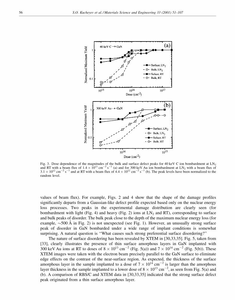
values of beam flux). For example, Figs. 2 and 4 show that the shape of the damage profilessignificantly departs from a Gaussian-like defect profile expected based only on the nuclear energyloss processes. Two peaks in the experimental damage distribution are clearly seen (forbombardment with light (Fig. 4) and heavy (Fig. 2) ions at LN2 and RT), corresponding to surfaceand bulk peaks of disorder. The bulk peak close to the depth of the maximum nuclear energy loss (forexample, �500 AÊ in Fig. 2) is not unexpected (see Fig. 1). However, an unusually strong surfacepeak of disorder in GaN bombarded under a wide range of implant conditions is somewhatsurprising. A natural question is `̀ What causes such strong preferential surface disordering?''
The nature of surface disordering has been revealed by XTEM in [30,33,35]. Fig. 5, taken from[33], clearly illustrates the presence of thin surface amorphous layers in GaN implanted with300 keV Au ions at RT to doses of 8� 1013 cmÿ2 (Fig. 5(a)) and 7� 1014 cmÿ2 (Fig. 5(b)). TheseXTEM images were taken with the electron beam precisely parallel to the GaN surface to eliminateedge effects on the contrast of the near-surface region. As expected, the thickness of the surfaceamorphous layer in the sample implanted to a dose of 7� 1014 cmÿ2 is larger than the amorphouslayer thickness in the sample implanted to a lower dose of 8� 1013 cmÿ2, as seen from Fig. 5(a) and(b). A comparison of RBS/C and XTEM data in [30,33,35] indicated that the strong surface defectpeak originated from a thin surface amorphous layer.
Fig. 3. Dose dependence of the magnitudes of the bulk and surface defect peaks for 40 keV C ion bombardment at LN2
and RT with a beam flux of 1:4� 1013 cmÿ2 sÿ1 (a) and for 300 keV Au ion bombardment at LN2 with a beam flux of3:1� 1012 cmÿ2 sÿ1 and at RT with a beam flux of 4:4� 1012 cmÿ2 sÿ1 (b). The peak levels have been normalized to therandom level.
56 S.O. Kucheyev et al. / Materials Science and Engineering 33 (2001) 51±107
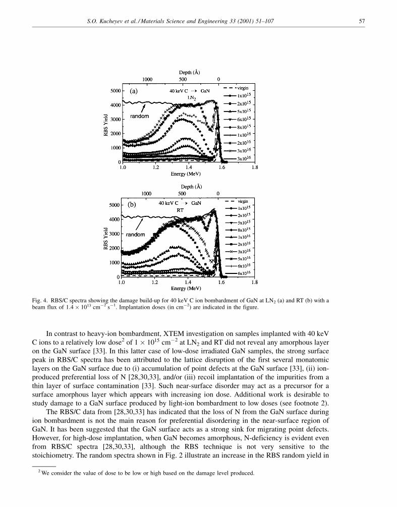
In contrast to heavy-ion bombardment, XTEM investigation on samples implanted with 40 keVC ions to a relatively low dose2 of 1� 1015 cmÿ2 at LN2 and RT did not reveal any amorphous layeron the GaN surface [33]. In this latter case of low-dose irradiated GaN samples, the strong surfacepeak in RBS/C spectra has been attributed to the lattice disruption of the first several monatomiclayers on the GaN surface due to (i) accumulation of point defects at the GaN surface [33], (ii) ion-produced preferential loss of N [28,30,33], and/or (iii) recoil implantation of the impurities from athin layer of surface contamination [33]. Such near-surface disorder may act as a precursor for asurface amorphous layer which appears with increasing ion dose. Additional work is desirable tostudy damage to a GaN surface produced by light-ion bombardment to low doses (see footnote 2).
The RBS/C data from [28,30,33] has indicated that the loss of N from the GaN surface duringion bombardment is not the main reason for preferential disordering in the near-surface region ofGaN. It has been suggested that the GaN surface acts as a strong sink for migrating point defects.However, for high-dose implantation, when GaN becomes amorphous, N-deficiency is evident evenfrom RBS/C spectra [28,30,33], although the RBS technique is not very sensitive to thestoichiometry. The random spectra shown in Fig. 2 illustrate an increase in the RBS random yield in
Fig. 4. RBS/C spectra showing the damage build-up for 40 keV C ion bombardment of GaN at LN2 (a) and RT (b) with abeam flux of 1:4� 1013 cmÿ2 sÿ1. Implantation doses (in cmÿ2) are indicated in the figure.
2 We consider the value of dose to be low or high based on the damage level produced.
S.O. Kucheyev et al. / Materials Science and Engineering 33 (2001) 51±107 57

the near-surface region with increasing ion dose. This has been assumed to reflect the loss of N fromthe surface during ion bombardment [28,30,33]. Moreover, N loss has also been observed by Augerelectron spectroscopy after plasma-induced etching of the GaN near-surface region [6,40].
2.4. Defect types
Damage produced in GaN by ion bombardment has been studied by XTEM in[14,16,21,22,27,30,32,33,35±39]. Fig. 6 shows XTEM images ((a), (c), (e) g � 0 0 0 2� and (b),(d), (f) g � 1 1 0 0�) taken from GaN implanted at RT with 300 keV Au ions with a beam flux of
Fig. 5. Cross-sectional bright-field XTEM images of GaN implanted with 300 keV Au ions at RT with a beam flux of4:4� 1012 cmÿ2 sÿ1 to doses of 8� 1013 cmÿ2 (a) and 7� 1014 cmÿ2 (b). Amorphous layers (labeled as A.L.) on the GaNsurface are clearly demonstrated. The thickness of the surface amorphous layer increases with increasing ion dose. Thecontrast of the XTEM has been adjusted to highlight the amorphous layers, but this causes loss of contrast for bulk depths.
Fig. 6. Dark-field ((a)±(d)) and bright-field ((e) and (f)) XTEM images ((a), (c), (e) g � 0 0 0 2� and (b), (d), (f)g � 1 1 0 0�) of the GaN epilayers bombarded at RT with 300 keV Au ions with a beam flux of 4:4� 1012 cmÿ2 sÿ1 todoses of 8�1013 cmÿ2 ((a) and (b)), 7� 1014 cmÿ2 ((c) and (d)), and 1:5� 1015 cmÿ2 ((e) and (f)).
58 S.O. Kucheyev et al. / Materials Science and Engineering 33 (2001) 51±107

4:4� 1012 to doses of 8� 1013 cmÿ2 (Fig. 6(a) and (b)), 7� 1014 cmÿ2 (Fig. 6(c) and (d)), and1:5� 1015 cmÿ2 (Fig. 6(e) and (f)). Some defect clusters are seen in the implanted region of thesample bombarded to the lowest dose of 8� 1013 cmÿ2 (Fig. 6(a)). XTEM images from the samplesimplanted to higher doses (7� 1014 and 1:5� 1015 cmÿ2) clearly illustrate point defect clusters(Fig. 6(c) and (e)) and a band of large planar defects (Fig. 6(d) and (f)) produced by heavy-ionbombardment. These planar defects are parallel to the basal plane of the GaN film. It is also seenfrom Fig. 6(d) that the region between the surface and the bulk defect peaks is free from planardefects. Fig. 6(e) and (f) illustrate a relatively thick surface amorphous layer (�400 AÊ thick) in thesample implanted to a dose of 1:5� 1015 cmÿ2. Fig. 6(f) also shows that, in the saturation regime forRT bombardment (see Fig. 2(b)), damage in the bulk consists of large planar defects in addition tosome defect complexes revealed in Fig. 6(e) taken under different diffraction conditions.
Fig. 7 shows dark-field XTEM images taken from GaN implanted at 5508C with 300 keV Auions to doses of 6� 1014 cmÿ2 (Fig. 7(a) and (b)) and 4� 1015 cmÿ2 (Fig. 7(c) and (d)). Theg � 0 0 0 2� XTEM images shown in Fig. 7(a) and (c) indicate the presence of point defect clusters inthe near-surface region (up to �1500 AÊ from the GaN surface). In addition, g � 1 1 0 0� XTEMimages from Fig. 7(b) and (d) again reveal implantation-produced planar defects. The concentrationof these planar defects, which again are parallel to the basal plane of the GaN film, increases withincreasing ion dose, as seen from a comparison of Fig. 7(b) and (d).
A similar band of planar defects, as shown in Figs. 6 and 7, has been observed in GaNbombarded with 40 keV C ions and with 100, 300, and 2000 keV Au ions at LN2 and RT [33,35],with 300 keV Au ions at 5508C [37], and with 2000 keV Cu ions at 5008C [39]. Consequently, it canbe concluded that these planar defects represent defect structures characteristic for GaN bombardedwith ions under a wide range of implant conditions. However, their microscopic structure andformation mechanisms are not understood at present and warrant additional systematic studies.These planar defects have been assumed to provide a `nucleation site' for amorphization with furtherincreasing ion dose during bombardment with light or heavy ions at LN2. However, it appears
Fig. 7. Dark-field XTEM images ((a), (c) g � 0002� and (b), (d) g � 1100�) of the GaN epilayers bombarded at 5508Cwith 300 keV Au ions with a beam flux of 3:1� 1012 cmÿ2 sÿ1 to doses of 6� 1014 cmÿ2 ((a) and (b)) and 4� 1015 cmÿ2
((c) and (d)).
S.O. Kucheyev et al. / Materials Science and Engineering 33 (2001) 51±107 59
energetically favorable for such planar defects to grow rather than to nucleate an amorphous phasefor heavy-ion irradiation at RT. Additional studies are highly desirable to understand the evolutionand saturation of defects in GaN during ion bombardment.
2.5. Effect of implant conditions
2.5.1. Ion mass
Given the current understanding of ion-beam-induced disordering processes in maturesemiconductor materials such as Si and GaAs, one can select two limiting cases based on thecharacteristics of the collision cascades generated by energetic ions penetrating through a crystal[41]. These two cases are bombardment with light and heavy ions relative to the masses of the hostatoms of the material under bombardment. In the case of light ions, collision cascades are very diluteand consist mostly of simple point defects such as vacancies and interstitials. In the case of heavyions, where the nuclear energy loss rate is large, it is generally believed that each ion generates adense collision cascade which, upon very fast cascade quenching, can often result in an amorphouszone [8±10]. Bombardment by intermediate mass ions represents a combination of these two limitingcases.
A detailed study of damage build-up in GaN under light (12C) and heavy (197Au) ionbombardment was recently reported in [33]. Indeed, the RBS/C data shown in Figs. 2±4 was takenfrom [33]. The following similarities between these two irradiation regimes have been pointed out[33].
1. Substantial dynamic annealing of ion-produced defects has been observed for both regimes atLN2 and RT.
2. For both irradiation regimes, the damage±depth profile, as measured by RBS/C, has two peaks Ðthe surface and bulk defect peaks. This feature has been attributed to high defect mobility andhigh efficiency of the GaN surface for trapping of migrating point defects [28,30,33].
3. In both cases, a band of planar defects nucleates in the crystal bulk with increasing ion dose.4. Similar damage build-up behavior at LN2 has been observed for both light and heavy ion
bombardment.
However, the following differences between light and heavy ion bombardment regimes havealso been revealed [33].
1. Completely different damage accumulation behavior has been observed for RT bombardment bylight (12C) and heavy (197Au) ions (see Figs. 2±4). No damage saturation in the GaN bulk duringirradiation with light ions has been observed, as measured by RBS/C. This fact may be explainedby the difference in the defects formed during bombardment with light and heavy ions (forexample, different size of planar defects). However, the chemical effects of implanted carbon and/or gold atoms may also influence the build-up of radiation damage in GaN, and this requiresadditional study.
2. A comparison of the disorder levels, as measured by RBS/C, with the results of TRIMcalculations [11] has shown that the defect annihilation efficiency is higher for light-ionbombardment than that for irradiation with heavy ions. This result is consistent with the fact thatthe defect generation rate is larger in the case of heavy-ion bombardment. Such an increase in thegeneration rate of defects enhances the rate of interaction between mobile defects, and,consequently, promotes the formation of defect complexes rather than defect annihilation viadynamic annealing.
60 S.O. Kucheyev et al. / Materials Science and Engineering 33 (2001) 51±107

3. Different dependencies of the magnitude of the surface defect peak on beam flux have beenobserved for light and heavy ions (see Section 2.5.4 for details).
2.5.2. Ion energyThe effect of ion energy on implantation disorder in GaN has been studied in [33,35]. Fig. 8
illustrates that the main features of damage build-up do not change upon increasing the energy of Auions from 100 to 2000 keV. One can see the same highly sigmodal damage build-up and thenucleation of two amorphous layers (surface and buried) for all three ion energies. In all three cases,the two amorphous layers Ð at the surface and in the bulk Ð nucleate and grow via a layer-by-layeramorphization process with increasing ion dose, as has been confirmed by XTEM [33,35].Ultimately, with further increasing ion dose, these two layers meet, resulting in a thick surface layerof amorphous material.
2.5.3. Implantation temperature
One way to avoid high levels of undesirable ion beam damage is elevated temperatureimplantation. This fact may explain why the effect of substrate temperature on implantation disorder
Fig. 8. RBS/C spectra illustrating the damage build-up in GaN bombarded at LN2 (a) by 100 keVAu ions with a beam fluxof 1:4� 1013 cmÿ2 sÿ1; (b) by 300 keV Au ions with a beam flux of 3:1� 1012 cmÿ2 sÿ1; and by 2000 keV Au ions with abeam flux of 5� 1012 cmÿ2 sÿ1. Implantation doses (in cmÿ2) are indicated in the figure.
S.O. Kucheyev et al. / Materials Science and Engineering 33 (2001) 51±107 61

in GaN has attracted particular interest. For example, Parikh et al. [17] studied, by RBS/C andXTEM, GaN bombarded with 120 keV Mg and 160 keV Si ions at 5508C. Suvkhanov et al. [20]reported a RBS/C study of GaN bombarded at 7008C with 100 keV Si and 80 keV Mg ions. A furtherreport by Wenzel et al. [26] concentrated on lattice disorder produced by a moderate dose of 90 keVMg ions implanted into GaN at temperatures up to 5508C, as studied by RBS/C. Finally, Kucheyevet al. [37] recently performed a study of damage build-up in GaN under 300 keV Au ionbombardment at 5508C. Results from [17,20,37] have shown that accumulation of stable defects andamorphization are indeed suppressed at elevated temperatures, as compared to implantation at roomtemperature and below. However, it is very interesting that, for high-dose ion implantation, dramaticion-beam-induced erosion of the GaN film has been reported [37], which will be discussed inSection 4.
Fig. 9, as well as Figs. 2±4, illustrates the effect of implantation temperature on disorder in GaNbombarded with 40 and 300 keV Au ions. It is seen from Figs. 2±4 that an increase in implantationtemperature from LN2 to RT not only reduces implantation damage but also dramatically changesthe damage build-up behavior. Indeed, no the damage saturation in the bulk has been observed in thecase of implantation with 300 keV Au ions at LN2 (see Fig. 2(a)). In addition, Fig. 9 shows that afurther increase in implantation temperature up to 5508C appreciably reduces the surface defect peakproduced by bombardment with 300 keV Au ions, while the bulk damage, as measured by RBS/C, ismuch less affected by implantation temperature in this temperature interval. This interesting effecthas been attributed to the temperature dependence of defect migration and agglomeration [35].
Fig. 10 shows selected RBS/C spectra that illustrate the damage build-up in GaN withincreasing dose of 300 keV Au ions at 5508C. It is seen that, for ion doses up to 6� 1014 cmÿ2, thedamage level both near the surface and in the bulk (with a maximum at �500 AÊ from the surface)gradually increases with increasing ion dose. For higher doses, both near-surface and bulk peaks ofdisorder exhibit saturation at levels which are considerably below the random level.
The microstructure of defects produced in GaN by 300 keV Au ion bombardment at 5508C waspreviously shown in Fig. 7. It is interesting that defect types and the damage build-up behavior in thebulk during 300 keVAu ion implantation at 5508C are, in fact, very similar to those observed in GaNbombarded with 300 keV Au ions at RT (see Figs. 2(b) and 6). However, in the case of RTimplantation, with increasing ion dose, amorphization proceeds layer-by-layer from the GaN surface,and, for a dose of 2:5� 1015 cmÿ2 of 300 keV Au ions, the whole implanted region is renderedamorphous. In the case of elevated temperature ion bombardment of GaN, amorphization is not
Fig. 9. RBS/C spectra illustrating the effect of implantation temperature on damage produced in GaN by 300 keV Au ionbombardment to a dose of 6� 1014 cmÿ2 with a beam flux of 4:4� 1012 cmÿ2 sÿ1. Implantation temperatures areindicated in the figure.
62 S.O. Kucheyev et al. / Materials Science and Engineering 33 (2001) 51±107

observed, but the behavior is more complex due to very efficient ion-beam-induced erosion of theGaN surface for high ion doses [37], as will be discussed in Section 4.
Despite the well-known weakness of the RBS/C technique for determining defect types, theRBS/C study by Wenzel et al. [26] concluded that the defects produced in GaN by 90 keV Mg ions at25, 300 and 5508C appeared to be the same. This result is in agreement with XTEM data from[33,37,39].
A comment should be made here on the apparent discrepancy in results on elevated temperatureion bombardment of GaN reported in [20,37,39]. Indeed, strong apparent surface disorderingobserved by RBS/C in [20] in GaN bombarded with 80 keV Mg and 100 keV Si ions at 7008C is notconsistent with more recent reports [37,39]. However, more detailed studies by a combination ofRBS/C, XTEM, and atomic force microscopy (AFM) techniques [42] have shown that, for elevatedtemperature bombardment, apparent strong surface disordering, as monitored by RBS/C, can occurbut is a result of C contamination of the GaN surface during ion bombardment. Special precautionsshould be made to suppress such C contamination during high-dose ion bombardment at elevatedtemperatures.
Another unexpected result has been reported by Wenzel et al. [26]. They have observed thatlattice disorder in GaN bombarded with 90 keV Mg ions increases with increasing implantationtemperature from RT up to 5508C. A somewhat similar effect of apparently increased damageproduced at RT compared to LN2 temperature for light-ion (40 keV C) bombardment to low doses(see footnote 2) was reported in [33]. These interesting results [26,28] may be qualitatively explainedbased on the fact that an increase in implantation temperature leads to an increase in the rate of allthermally activated point defect processes (defect diffusion, direct and indirect annihilation,formation of complexes, trapping of free defects by defect complexes and impurities, etc.). Thenature of `stable' defect complexes formed at RT or elevated temperatures during dynamic annealingmay, as a consequence, result in a higher level of residual disorder. However, at present, furtherexperimental work is necessary to identify the most plausible mechanism for this somewhat oddtemperature-dependent effect.
2.5.4. Beam flux
The effect of beam flux on lattice disorder in GaN has been reported in [26,33,35]. Fig. 11shows RBS/C spectra illustrating the effect of beam flux on implantation damage produced by
Fig. 10. RBS/C spectra showing the damage build-up for 300 keVAu ion bombardment of GaN at 5508C with a beam fluxof 3:1� 1012 cmÿ2 sÿ1. Implantation doses (in cmÿ2) are indicated in the figure. The positions of the surface peaks of Gaand Au are shown by arrows.
S.O. Kucheyev et al. / Materials Science and Engineering 33 (2001) 51±107 63

300 keV Au ion bombardment of GaN at LN2 (Fig. 11(a)) and RT (Fig. 11(b)). It is seen that, withincreasing beam flux, the magnitude of the bulk defect peak also increases for both LN2 and RTimplantation regimes (the so-called normal flux effect when the damage level increases uponincreasing beam flux). This normal flux effect is consistent with the current understanding of ionbeam damage build-up in semiconductors under implantation conditions when substantial dynamicannealing of radiation defects takes place (see, for example [4,43]). An increase in beam fluxdecreases the average time interval between collision cascades which spatially overlap. Such anincrease in the generation rate of point defects with increasing beam flux enhances the rate ofinteractions between mobile defects and, therefore, enhances the formation of defect complexes.
However, Fig. 11(b) also shows that, for RT irradiation, the surface defect peak decreases inmagnitude with increasing beam flux. This reverse flux effect, observed also in the case of light-ionbombardment of GaN at LN2 [33,35], strongly supports the important role of mobile point defects inthe formation and growth of a surface amorphous layer in GaN under ion bombardment. This reverseflux effect has been qualitatively explained in terms of the competition between defect trapping andmigration processes [33]. Indeed, an increase in beam flux enhances the formation of defectcomplexes in the crystal bulk, and fewer point defects can reach the surface. However, Fig. 11(a)shows a normal flux effect for the surface defect peak in GaN under irradiation at LN2. This has beenattributed to smaller effective diffusion lengths of point defects at LN2, as compared to ionirradiation at RT, where a reverse flux effect has been observed (Fig. 11(b)) [33].
Wenzel et al. [26] have reported that variation of beam flux (from 3:1� 1012 to1:3� 1014 cmÿ2 sÿ1) of 90 keV Mg ions implanted into GaN at RT has no effect on damagemeasured by RBS/C. Although this result seems to be somewhat surprising (at least the effects ofbeam heating could become pronounced for the largest beam flux used), it is consistent with the
Fig. 11. RBS/C spectra of GaN implanted with 300 keV ions to a dose of 3� 1014 cmÿ2 at LN2 (a) and RT (b). The valuesof beam flux are indicated in the figure. The figure illustrates the reverse and normal flux effects.
64 S.O. Kucheyev et al. / Materials Science and Engineering 33 (2001) 51±107

independence of implantation disorder on beam flux for light-ion (40 keV C) bombardment of GaNat RT [42].
2.6. Comparison with damage build-up in Si and GaAs
Finally, we make a brief comparison of implantation disorder build-up in GaN with that in muchmore extensively studied semiconductors Ð Si and GaAs [33]. All the experimental data onimplantation damage in GaN indicates very strong recovery of ion-generated defects in GaN duringion bombardment even at LN2. In contrast to Si or GaAs, GaN is extremely difficult to amorphize byion bombardment. For example, amorphous layers in Si or GaAs can be created by heavy-ionbombardment at RT to doses of the order of 1014 cmÿ2, while GaN remains crystalline to muchhigher ion doses (see for example Figs. 2, 3 and 6). This is a direct consequence of very efficientdynamic annealing processes in GaN during ion bombardment. However, dynamic annealing isnever perfect. With increasing ion dose, GaN exhibits layer-by-layer amorphization proceeding fromthe surface, as well as the nucleation and growth of a band of extended defects in the bulk [33].
Some features of damage build-up in GaN at LN2 resemble those occurring in Si or GaAsduring elevated temperature ion bombardment. Indeed, during elevated temperature ion bombard-ment of these latter materials, when dynamic annealing of ion-generated defects is strong, damageaccumulation proceeds via the formation of an array of extended defects, as has been reviewedelsewhere [4,33,43]. These extended defects in Si or GaAs are usually tangles of dislocations, andtheir density increases with increasing ion dose. Depending on implant conditions, this can cause acontinuous rise in the total energy of the system until it collapses into the energetically morepreferable amorphous state [44]. In addition, in both Si and GaAs, layer-by-layer amorphization canproceed from the surface. In this case, the surface acts as a `nucleation site' for amorphization.
Thus, the scenario for amorphization in GaN under ion bombardment even at LN2 appears to bequalitatively similar to that in Si or GaAs at elevated implant temperatures [33]. Indeed, damageevolution in GaN proceeds via the formation of a band of extended defects under a wide range ofimplant conditions [33,35,37,39]. The surface of GaN also acts as a `nucleation site' foramorphization [14,15,28±30,33,35,39]. However, the ion-produced extended defects in GaN consistof a regular array of planar defects, not dislocation tangles as in Si or GaAs. Moreover, the presenceof a saturation regime during RT bombardment of GaN with heavy ions may suggest that the processof amorphization in GaN is more complex than that in Si or GaAs during elevated temperaturebombardment. Indeed, in addition to the possible chemical effects of implanted atoms,amorphization of GaN seems to be stimulated by the processes of local stoichiometric imbalance,which becomes pronounced for high ion doses [33,36,39]. This may explain why amorphous zones,expected from the quenching of dense collision cascades produced by heavy ions, appear to beunstable in GaN, whereas surface and buried amorphous layers can be nucleated for very high iondoses. However, it is obvious that, at present, more experimental work is necessary for a deeperunderstanding of amorphization mechanisms in GaN.
A comment should be made on the possibility of developing a quantitative model for damagebuild-up in GaN. It is clear that all `traditional' quantitative models (see, for example [41,45,46]) canbe applied only when the rate of dynamic annealing is considerably lower than the defect productionrate, which is not the case even for heavy-ion bombardment of GaN at LN2. At present, thedevelopment of a model which takes into account elemental defect processes and dynamic annealingin GaN during ion bombardment appears to be a rather difficult task, due to a very limitedunderstanding of these processes. A satisfactory quantitative model must wait for furtherexperimental insight.
S.O. Kucheyev et al. / Materials Science and Engineering 33 (2001) 51±107 65

3. Ion-beam-induced porosity
AFM and XTEM results reported in [32,36,39] have shown that high-dose ion bombardment ofepitaxial GaN films with heavy ions results in anomalous swelling of the implanted region. Forexample, an AFM image in Fig. 12 illustrates the border between implanted (on the left) andunimplanted (on the right) areas of a GaN sample bombarded with 2 MeV Au ions at LN2 to a doseof 1� 1016 cmÿ2. As clearly seen, ion implantation has caused pronounced material swelling with astep height as large as �1700 AÊ . In addition, the implanted area exhibits large-scale roughness. InFig. 13 the dose dependence of the step height between implanted and unimplanted regions of2 MeV Au ion bombarded GaN is shown. It is seen that a rapid step height increase occurs for iondoses above �3� 1015 cmÿ2.
In Fig. 14 bright-field XTEM images of GaN bombarded with 2 MeV Au ions at LN2 to threedifferent doses are shown. Note that all three images were taken with the same magnification. TheXTEM image from Fig. 14(a) (a dose of 5� 1015 cmÿ2) clearly shows two amorphous layers Ðsurface and buried Ð separated by a layer of heavily damaged, but still crystalline material. Theimages from Fig. 14(b) and (c), which are for higher ion doses (doses of 1� 1016 and3� 1016 cmÿ2, respectively), reveal that ion bombardment to these doses results in the formation ofamorphous layers continuous to the surface. Detailed XTEM and electron diffraction investigationperformed in [36] showed that these layers were completely amorphous.
Fig. 14 clearly illustrates that GaN amorphized by heavy-ion bombardment is porous. Theamorphous layers have voids or gas bubbles, which are close-to-spherical in shape. The averageradius of the voids/bubbles increases according to the nuclear energy loss profile of Au ions. Acomparison of Fig. 14(a)±(c) indicates that, with increasing ion dose, the size of the voids/bubblesalso increases. Fig. 14 also suggests that small voids/bubbles agglomerate into larger ones withincreasing ion dose.
As reported in [32], the onset of the large step height, with increasing ion dose, coincides withthe nucleation of a buried amorphous layer in the region of the maximum nuclear energy loss.Moreover, a rapid step height increase in the dose range from �3� 1015 to �7� 1015 cmÿ2 (seeFig. 13) corresponds to the dose interval in which buried and surface amorphous layers expand and
Fig. 12. A tapping mode AFM image illustrating the border between implanted (on the left) and unimplanted (on the right)areas of a GaN sample bombarded with 2 MeV Au ions at LN2 to a dose of 1� 1016 cmÿ2 with a beam flux of5� 1012 cmÿ2 sÿ1.
66 S.O. Kucheyev et al. / Materials Science and Engineering 33 (2001) 51±107
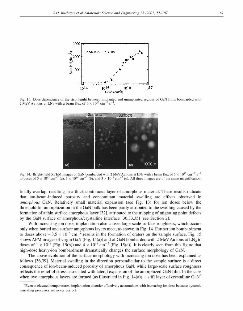
finally overlap, resulting in a thick continuous layer of amorphous material. These results indicatethat ion-beam-induced porosity and concomitant material swelling are effects observed inamorphous GaN. Relatively small material expansion (see Fig. 13) for ion doses below thethreshold for amorphization in the GaN bulk has been partly attributed to the swelling caused by theformation of a thin surface amorphous layer [32], attributed to the trapping of migrating point defectsby the GaN surface or amorphous/crystalline interface [30,33,35] (see Section 2).
With increasing ion dose, implantation also causes large-scale surface roughness, which occursonly when buried and surface amorphous layers meet, as shown in Fig. 14. Further ion bombardmentto doses above �3:5� 1016 cmÿ2 results in the formation of craters on the sample surface. Fig. 15shows AFM images of virgin GaN (Fig. 15(a)) and of GaN bombarded with 2 MeVAu ions at LN2 todoses of 1� 1016 (Fig. 15(b)) and 4� 1016 cmÿ2 (Fig. 15(c)). It is clearly seen from this figure thathigh-dose heavy-ion bombardment dramatically changes the surface morphology of GaN.
The above evolution of the surface morphology with increasing ion dose has been explained asfollows [36,39]. Material swelling in the direction perpendicular to the sample surface is a directconsequence of ion-beam-induced porosity of amorphous GaN, while large-scale surface roughnessreflects the relief of stress associated with lateral expansion of the amorphized GaN film. In the casewhen two amorphous layers are formed (as illustrated in Fig. 14(a)), a stiff layer of crystalline GaN3
Fig. 13. Dose dependence of the step height between implanted and unimplanted regions of GaN films bombarded with2 MeV Au ions at LN2 with a beam flux of 5� 1012 cmÿ2 sÿ1.
Fig. 14. Bright-field XTEM images of GaN bombarded with 2 MeVAu ions at LN2 with a beam flux of 5� 1012 cmÿ2 sÿ1
to doses of 5� 1015 cmÿ2 (a), 1� 1016 cmÿ2 (b), and 3� 1016 cmÿ2 (c). All three images are of the same magnification.
3 Even at elevated temperatures, implantation disorder effectively accumulates with increasing ion dose because dynamic
annealing processes are never perfect.
S.O. Kucheyev et al. / Materials Science and Engineering 33 (2001) 51±107 67

separating these two amorphous layers prevents film deformation and, therefore, prevents theappearance of large-scale surface roughness, as consistent with AFM data from [36]. Finally, surfacecraters observed on samples implanted to high ion doses (�3:5� 1016 cmÿ2; see Fig. 15(c)) may beformed when voids/bubbles increase in size and intersect the surface.
Fig. 15. Height-mode AFM images of virgin GaN (a) and of GaN bombarded with 2 MeVAu ions at LN2 with a beam fluxof 5� 1012 cmÿ2 sÿ1 to doses of 1� 1016 cmÿ2 (b) and 4� 1016 cmÿ2 (c).
68 S.O. Kucheyev et al. / Materials Science and Engineering 33 (2001) 51±107
It should be noted that similar porous structures have also been observed in GaN filmsamorphized by 300 keV Au ion bombardment [32,36]. However, in this latter case of keV heavy-ionbombardment, the ion penetration depth is significantly smaller than that in the case of MeV ionirradiation, which makes the material swelling less pronounced. A combination of XTEM, RBS/C,and AFM data has shown that ion-beam-induced volume expansion of amorphous GaN can be aslarge as �50% [32,36,39].
The effects of ion-beam-induced porosity and concomitant material expansion reported in[32,36,39] are, in fact, not new. Similar effects have been observed in some other semiconductors,such as Ge [47,48], InSb [49], and GaSb [50]. In general, amorphousness is not necessarily the finalstate of a semiconductor exposed to ion bombardment. Although, studied in some detail (particularlyin the case of Ge [49]), ion-beam-induced evolution of porous structures in amorphous materials isnot well-understood. One of the possible explanations for this effect is energetically favorableagglomeration of vacancy-like defects, generated by an ion beam in an amorphous matrix, resultingin the formation of voids [47,48,51]. However, in the case of GaN, ion-beam-induced porosity hasbeen attributed to material decomposition with the formation of N2 gas bubbles in a Ga-rich matrixduring heavy-ion bombardment [36,39].
Such a conclusion that the porosity of GaN is due to the formation of N2 gas bubbles in anamorphous GaN matrix is supported by the evolution of the porous structure with increasing iondose, as studied by XTEM (see Fig. 14). Indeed, as studied in the cases of ion-beam-induced porosityof Ge, InSb, and GaSb [47±50], the evolution of voids, with increasing ion dose, proceeds via theformation of a sponge-like structure with voids having an elongated, irregular shape. For example,the voids in Ge appear to repel each other as they increase in size [48]. In our case of GaN, the voids/bubbles are spherical in shape for a wide range of ion doses (see Fig. 14), which is typical for thecase of the formation of gas bubbles. This conclusion has also been supported by the annealingbehavior of porous GaN as well as by RBS/C data [36,39]. Indeed, RBS/C spectra taken from GaNamorphized by heavy ions (see Fig. 2(a)) have a `shoulder' with a decreased RBS/C yield in the ionend-of-range region (a region with large bubbles) and increased yield near the GaN surface(presumably, a Ga-rich region). If a porous layer had voids (not bubbles), no `shoulder' in the RBS/Cspectra would be expected [13].
The formation of N2 gas bubbles has been explained by the well-known effect of ion-beam-induced stoichiometric imbalance [36,39]. Indeed, local stoichiometric imbalance in the collisioncascade volume may produce an excess concentration of the heavier element at shallow depth, whilethe region at greater depth is enriched with atoms of the lighter element. This effect is greatest whenthe mass ratio of the constituent elements of the semiconductor is high, and when the ion mass islarge [52]. Therefore, for the case of 2 MeV 197Au ion bombardment of GaN Ð a material with alarge difference in the masses of constituent elements (70Ga and 14N) Ð the effect of localstoichiometric imbalance can readily account for the formation of N2 gas bubbles in a highly N-deficient GaN matrix, as was predicted in [33].
However, the final stoichiometry after ion bombardment also depends on defect migration, notonly on the ballistic collisional processes. The data from [32,36,39] suggests that, beforeamorphization, stoichiometric disturbances in crystalline GaN are very effectively repaired viadefect diffusion and dynamic annealing processes. Such dynamic annealing has been shown to beextremely efficient in crystalline GaN (see Section 2). Ion-beam-induced stoichiometric disturbancesbecome evident only after GaN is amorphized (see Fig. 14(a)), as has been shown in [32,36,39].
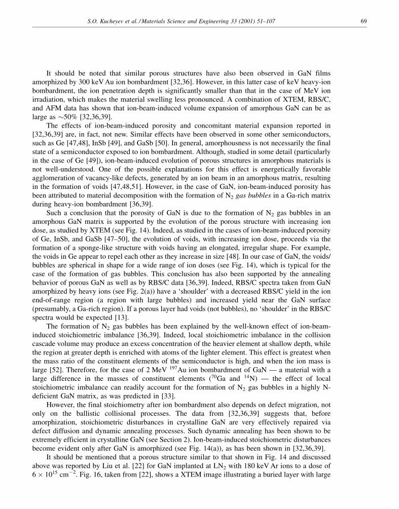
It should be mentioned that a porous structure similar to that shown in Fig. 14 and discussedabove was reported by Liu et al. [22] for GaN implanted at LN2 with 180 keV Ar ions to a dose of6� 1015 cmÿ2. Fig. 16, taken from [22], shows a XTEM image illustrating a buried layer with large
S.O. Kucheyev et al. / Materials Science and Engineering 33 (2001) 51±107 69

bubbles/voids embedded. Liu et al. [22] claimed that the whole layer (a) in Fig. 16 was amorphousand interpreted the porous-like structure as Ar bubbles. However, in view of the results discussedabove, the structure shown in Fig. 16 is more likely to consist of a large concentration of N2 gasbubbles embedded in an amorphous matrix. Indeed, for a dose of 6� 1015 cmÿ2 of 180 keV Ar ions,it is very difficult to expect a high concentration of large Ar gas bubbles as shown in Fig. 16. It ismore reasonable to interpret Fig. 16 in terms of the phenomenon of ion-beam-induced porosity inGaN. Hence, GaN amorphized with intermediate-mass ions (such as Ar), not only with heavy ions asillustrated earlier in this section, exhibits porosity.
4. Ion-beam-induced erosion
As mentioned above, high-dose ion bombardment of GaN is accompanied by very efficienterosion of the GaN surface. This interesting effect was reported in [37,38,39]. Fig. 17, taken from[37], shows the dose dependence of the step height between implanted and unimplanted regions ofGaN bombarded with 300 keV Au ions at 5508C, as measured by AFM. This figure illustratesanomalous surface erosion, which occurs for high ion doses. For example, it is seen that such ionbombardment to a dose of 1� 1016 cmÿ2 results in the erosion of a �1000 AÊ thick surface layer.
Fig. 16. A bright-field XTEM image of GaN implanted at LN2 with 180 keV Ar ions to a dose of 6� 1015 cmÿ2.
Fig. 17. The dose dependence of the step height between implanted and unimplanted regions of GaN films bombardedwith 300 keV Au ions at 5508C with a beam flux of 3:1� 1012 cmÿ2 sÿ1. This figure illustrates that high-dose ionimplantation is complicated by very efficient material erosion.
70 S.O. Kucheyev et al. / Materials Science and Engineering 33 (2001) 51±107

This anomalous erosion also explains the somewhat unexpected shape of the RBS/C spectra of GaNimplanted at 5508C to high ion doses, as illustrated in Fig. 10 for the case of a sample implanted to adose of 2� 1016 cmÿ2. Indeed, due to erosion, the position of the GaN surface changes withincreasing ion dose, and both disorder and Au profiles are shifted towards the surface [37].
It is clear that ballistic sputtering mechanisms alone cannot account for such a large sputteringyield for high ion doses (see Fig. 17) [53]. Instead, this anomalous surface erosion has beenattributed to a three-step process of (i) the build-up of implantation disorder with increasing iondose4 (ii) thermally- and ion-beam-induced decomposition of a heavily damaged near-surface layerfor relatively high ion doses, and (iii) ion-beam-induced erosion of such a decomposed (N-deficient)layer [37±39]. This three-step scenario is consistent with recent ion-beam-induced erosionobservations for both amorphous and heavily damaged GaN films. For example, RBS/C data from[38] has shown that the thickness of amorphous layers, produced by low temperature heavy-ionbombardment, reduces almost linearly with increasing dose of 2 MeV Cu ions implanted at 5008C.In addition, Fig. 18 illustrates the temperature dependence of the reduction in the amorphous layerthickness for 2 MeV Cu ion bombardment to a dose of 1� 1016 cmÿ2. A XTEM investigation [38]of these samples has shown that such a reduction in the thickness of amorphous layers is due toenhanced ion-beam-induced erosion of the GaN surface, rather than due to ion-beam-inducedepitaxial crystallization (IBIEC) [54]. Therefore, data reported in [37±39] indicates that GaN crystalswith damage levels above some threshold value exhibit very efficient erosion during elevatedtemperature ion bombardment. This efficient erosion may impose significant limitations on thetechnological applications of `hot implants' into GaN.
5. Mechanical properties
There has been considerable interest in determining the mechanical properties of GaN. Indeed,studies of the processes controlling contact damage, wear, and cracking of GaN layers have significanttechnological importance. Moreover, understanding the deformation behavior of ion-beam-modifiedGaN is not only important for contact damage issues in the GaN industry but is also necessary forunderstanding the evolution of the structural characteristics of GaN under ion bombardment.
Fig. 18. An Arrhenius plot of the rate of reduction of the amorphous layer thickness for 2 MeV Cu ion bombardment for adose of 1� 1016 cmÿ2.
4 The mechanical properties of ion-beam-modified GaN, supporting this discussion, will be discussed in Section 5.
S.O. Kucheyev et al. / Materials Science and Engineering 33 (2001) 51±107 71

The mechanical properties of semiconductors are usually studied (i) by conventional Vickersmicro-hardness testing, or (ii) by continuous-depth-sensing indentation testing (generally known asnanoindentation), which is a much more powerful technique. Indeed, nanoindentation is capable ofproviding information on a range of mechanical properties such as hardness and elastic propertiesand their variation continuously with indenter penetration depth. Such information can be readilyobtained directly from force±displacement measurements. In addition, nanoindentation is ideal formeasuring the mechanical properties of very thin films. It is well-known that, if the substrate isharder than the film, the substrate influence is usually negligible when the penetration depth of theindenter is less than �10% of the film thickness [55].
Several studies of the mechanical properties of as-grown GaN [56±63] and ion-beam-modifiedGaN [64] have been reported in the literature. In this section, we discuss the mechanical properties of(i) as-grown GaN, (ii) crystalline GaN with a relatively high concentration of implantation-produceddefects, and (iii) GaN amorphized by ion bombardment. It is interesting that, unlike the situation forSi [65], implantation damage dramatically changes the deformation behavior of GaN.
Table 3 gives the values of hardness and Young's modulus of as-grown GaN in comparison withthe values for some other semiconductors. It is seen from this table that as-grown GaN is a relativelyhard material. In addition, recent nanoindentation data [63] has shown that cracks are not nucleatedin GaN epilayers even for loads as large as 900 mN with an �4.2 mm spherical indenter, whichsupports a large fracture toughness of this material in the as-grown state.
Fig. 19 shows typical continuous load±unload force±displacement curves of as-grown(Fig. 19(a)), `ion-damaged' (Fig. 19(b)), and amorphized (Fig. 19(c)) GaN films. Such an `ion-damaged' sample, with a relatively high concentration of implantation-produced defects (but notamorphous), was prepared by multiple-energy bombardment with 197Au ions at 3008C. The implantconditions used to prepare this sample are given in Table 4. Such a multiple-energy implantationprocedure at an elevated temperature results in the formation of lattice defects, including someplanar defects, up to �1 mm from the surface (see Section 2). It should be noted that, for the iondoses used to prepare this sample, the concentration of implanted Au species (<0.06 at.%) isexpected to have a negligible effect on the mechanical properties of GaN. Rather, the deformationbehavior of ion-beam-modified GaN should be determined by implantation-produced lattice disorderand its consequences.
To prepare an amorphous layer shown in Fig. 19(c), GaN was bombarded with 2 MeV 197Auions at LN2 with a beam flux of 5� 1012 cmÿ2 sÿ1 to a dose of 1:5� 1016 cmÿ2. Such implantationresults in the formation of an �0.6 mm thick, completely amorphous surface layer [32,36,65]. It
Table 3
The values of hardness, H, and Young's modulus, E, of as-grown GaN in comparison with the values for some other
semiconductorsa
Semiconductor H (GPa) E (GPa) Plastic penetration (nm)
GaN 13.4 233 100Si 11.5 150 100Ge 8.8 118 100GaAs 7 94 200InP 4.8 77 200GaP 9.6 113 300
a Data is taken from [63,64,66]. In all the cases, nanoindentation was done with the same spherical indenter, as
described in detail elsewhere [64]. The values are chosen for indenter penetration after the `pop-in' event, as indicated in
the last column.
72 S.O. Kucheyev et al. / Materials Science and Engineering 33 (2001) 51±107

should be noted that GaN amorphized under these conditions should exhibit some degree of porosity(see Section 3), which may also affect the deformation behavior as discussed below.
Fig. 19(a) clearly illustrates that a discontinuity (or `pop-in') of the yield response occurs duringloading of as-grown GaN. This result is in agreement with other nanoindentation data reported in theliterature for GaN, as discussed in detail in [63,64]. Interestingly, Fig. 19(b) reveals that in `ion-damaged' GaN, the `pop-in' event is still present but significantly less pronounced than in as-grownGaN. Finally, Fig. 19(c) shows no discontinuities in the load±displacement curve of amorphous GaN,in full agreement with the expected deformation behavior of an amorphous solid [65].
Typical amplitude-mode AFM images of as-grown (Fig. 20(a)) and `ion-damaged' (Fig. 20(b))GaN films indented at a maximum load of 100 mN are shown in Fig. 20. These AFM images clearlyillustrate that slip, which occurs during loading of as-grown GaN, is strongly suppressed in `ion-damaged' GaN. A comparison of nanoindentation data (see Fig. 19(a) and (b)) and AFM data (seeFig. 20) gives a compelling argument that slip nucleation (rather than a phase transformation) is thephysical mechanism responsible for the `pop-in' events observed during loading of GaN, asdiscussed more fully in [63,64].
Fig. 19. Typical continuous load±unload curves of (a) as-grown, (b) `ion-damaged', and (c) amorphized GaN films. Notethat the maximum load is 100 mN for (a) and (b) and is 40 mN for (c).
Table 4
The implant conditions used to prepare the `ion-damaged' sample by multiple-energy bombardment with 197Au ions at
3008C
Energy (MeV) Dose (1014 cmÿ2) Beam flux (1012 cmÿ2 sÿ1)
6.6 7 5.22 3 180.45 5 17
S.O. Kucheyev et al. / Materials Science and Engineering 33 (2001) 51±107 73

Fig. 21 shows the curves of the average contact pressure (or (Meyer) hardness), H (Fig. 21(a)),and Young's modulus, E (Fig. 21(b)), as a function of indenter penetration below the circle ofcontact, as determined from the partial load±unload data. This figure, showing data for as-grown,`ion-damaged', and amorphized GaN, reveals that ion bombardment dramatically modifies H and E.It is seen that, for shallow penetration depths of the indenter (prior to the `pop-in' event), the H and E
values of `ion-damaged' GaN are lower than those of as-grown material. As expected, the value of Eis not affected by slip and remains essentially constant for the whole indenter penetration depth5.However, slip significantly affects H of as-grown GaN, while in `ion-damaged' GaN slip is stronglysuppressed, and, for larger depths of indenter penetration, H becomes larger than that of as-grown
Fig. 20. Typical amplitude-mode AFM images of (a) as-grown and (b) `ion-damaged' GaN films indented at a maximumload of 100 mN (horizontal field width is 4 mm for both images (a) and (b)).
Fig. 21. The curves of (a) the hardness and (b) Young's modulus as a function of indenter penetration below the circle ofcontact, as determined from the partial load±unload data. Figures show data for as-grown, `ion-damaged', and amorphizedGaN, as indicated in the legend in (a).
5 Slightly non-constant behavior for E of ion-damaged GaN with increasing penetration depth (see Fig. 21(b)) may be
attributed to a non-uniform distribution of implantation disorder and/or to the substrate effect.
74 S.O. Kucheyev et al. / Materials Science and Engineering 33 (2001) 51±107
GaN. Fig. 21 also shows that the values of H and E of amorphized GaN are significantly lower thanthose of as-grown and `ion-damaged' GaN; i.e. amorphous GaN is very soft. Table 5 gives the valuesof H and E for the above three GaN samples at a plastic penetration depth of 100 nm, a depth wheresubstrate effects are expected to be small.
Finally, a close examination of partial load±unload curves reveals that, in `ion-damaged' GaN,the purely elastic regime extends to higher loads and penetration depths than in as-grown GaN. Thisresult indicates that implantation disorder in crystalline GaN somewhat suppresses pressure-inducednucleation and/or propagation of extended defects, the processes which are most likely responsiblefor the plastic deformation of crystalline GaN [61±64]. In contrast, in amorphized GaN, deformationresponse is elastic±plastic even for very low loads, and, with increasing load, plastic deformationdominates, with pile-up around the impression (as revealed by AFM), typical for indentation ofamorphous solids. Such a difference in the deformation modes of as-grown, `ion-damaged', andamorphized GaN is also reflected by the depths of residual depression (see Figs. 19 and 20) and thedepths of maximum plastic penetration (see Fig. 21) of the above three samples.
6. Annealing of implantation damage
In the semiconductor industry, ion implantation used for electrical and optical doping is alwaysfollowed by an annealing step. Such annealing is necessary (i) to remove implantation-producedlattice disorder and (ii) to electrically/optically activate implanted species by stimulating theirmigration into energetically favorable lattice sites. Post-implantation annealing is a very importanttechnological step since device performance is highly dependent on the efficiency of such annealing.Below, we briefly discuss the main results reported in the literature on the annealing of ion implantedGaN. As in previous sections of this review, we emphasize recent data, not discussed in the previousreviews. We will also discuss here only the structural characteristics of GaN, while the effects ofannealing on the optical and electrical characteristics of ion implanted GaN will be reviewed in thefollowing sections.
6.1. Approaches to annealing of GaN
Annealing of implantation disorder in GaN is expected to be difficult. Indeed, a general rule ofthumb, which is well-known from the 1970s, is that temperatures of �2/3 of the melting point (in K)are required to remove extended defects in semiconductors. Because the melting point of GaNappears to be very high (�25008C, based on calculations by Van Vechten [67]), one can expect thatannealing temperatures of �16508C are necessary to remove implantation-produced disorder inGaN. At such high temperatures, annealing of GaN is complicated by material decomposition; i.e. byloss of nitrogen from the GaN surface [1±3,5]. Such surface decomposition of as-grown GaN
Table 5
The values of hardness, H, and Young's modulus, E, at a plastic penetration depth of 100 nm for the three GaN samples
described in the text
GaN sample H (GPa) E (GPa)
As-grown 13.4 233`Ion-damaged' 15.1 164Amorphized 2.4 65
S.O. Kucheyev et al. / Materials Science and Engineering 33 (2001) 51±107 75

becomes pronounced for prolonged anneals at temperatures of above �8008C6. Suppression of thesurface degradation of GaN during annealing is a challenging problem, given the high temperaturesrequired to remove implantation-produced disorder.
Many attempts to anneal implantation damage in GaN have been reported in the literature[15,17,19,21,23,26±28,31,34,36,38,39,68±92] as summarized in Table 6 for the case of the studies ofstructural characteristics. It is seen from this table that both conventional furnace annealing and rapidthermal annealing (RTA) have been tried, using mostly annealing temperatures up to 12008C. Thismaximum annealing temperature of 12008C reflects the maximum temperatures usually used in Siand GaAs technologies and the fact that commercial RTA equipment is limited to this temperature.
Table 6 also shows that the following methods have been used to protect GaN fromdecomposition: (i) the proximity geometry, where GaN samples are placed face-to-face, (ii)annealing of GaN within a SiC-coated graphite susceptor which contains powdered AlN or InN toproduce a pressure of nitrogen over GaN, (iii) annealing of GaN in an evacuated quartz ampoulecontaining elementary Al, (iv) annealing under extreme conditions of nitrogen overpressure (up to�15 kbar), and (v) capping of GaN surface (before annealing) with a protective layer of anothermaterial. Examples of annealing behavior given below will support the expectation that annealingtemperatures above 15008C are necessary for a complete removal of implantation disorder in GaN.At such high temperatures, the only methods which have shown some success to suppressdecomposition of GaN are (i) an overpressure of nitrogen (up to 15 kbar) and (ii) capping of GaNsurface with AlN layers. The other methods tried cannot protect GaN from decomposition at suchhigh temperatures (�15008C)7. Therefore, normal RTA equipment used for annealing attemperatures up to 12008C is not geared towards the requirements of GaN (i.e. RTA at temperaturesat or above �15008C or annealing at such temperatures under a large nitrogen overpressure).
6.2. Annealing of pre-amorphous disorder
All the results on the annealing of implantation-produced disorder in GaN indicate thatannealing temperatures below �12008C are not sufficient to completely remove damage producedeven by low-dose implantation (see footnote 2). For example, Fig. 22 illustrates bright-field XTEMimages of a GaN sample bombarded with 90 keV Si ions at LN2 to a dose of 6� 1015 cmÿ2. Shownin Fig. 22(a) and (b) are images before and after post-implantation annealing at 11008C for 30 s,respectively. Fig. 22(a) shows that such Si ion implantation produced a dense network of defectclusters in the implanted layer, while Fig. 22(b) indicates that annealing at 11008C does not removethese defects. This has also been confirmed by RBS/C [15]. For example, the annealing of GaNimplanted with 90 keV Mg and 180 keV Ca ions was studied by RBS/C in [26,27,31]. It has beenshown that significant (but always only partial) recovery of implantation damage by annealing at11008C for 15 s in a nitrogen ambient is possible only after very low dose ion implantation (seefootnote 2). Such low doses are found to produce very dilute disorder observed by XTEM and RBS/C [33]. Thus, annealing at relatively low temperatures (below �12008C) is only effective insignificantly reducing implantation damage produced by low-dose ion implantation, before thenucleation of planar defects. For larger ion doses, when a band of extended defects nucleates in the
6 However, the temperature where decomposition of GaN becomes pronounced strongly depends on the defect state of
the material as well as on the annealing ambient.7 It should be noted that success achieved with preventing decomposition of GaN by capping the GaN surface with AlN
layers is still limited because of a problem with ex-foliation of AlN layers during such an ultra-high temperature RTA
treatment.
76 S.O. Kucheyev et al. / Materials Science and Engineering 33 (2001) 51±107

crystal bulk [33], much higher annealing temperatures are required for even partial removal ofdefects.
RBS/C results discussed in [91] have shown that RTA annealing at 14008C for 30 s of GaN(capped with AlN) implanted with 210 keV Si ions to a dose of 5� 1015 cmÿ2 at RT resulted in onlya partial recovery of implantation-produced lattice disorder. The only report on a successful (and anapparently complete) recovery of implantation damage (produced by 100 keV Si ion implantation toa dose of 5� 1015 cmÿ2 at RT) involved post-implantation annealing at 15008C for 15 min under anitrogen overpressure of �15 kbar [1]. After such an annealing, the sample had an RBS/C yieldequivalent to an unimplanted sample, with no macroscopic surface decomposition [1]. The annealingof damage was also supported by photoluminescence and Hall effect measurements. For the firsttime, this result has demonstrated that implantation disorder can be effectively removed by ultra-high
Table 6
Studies of thermal annealing of GaN (structural characteristics)
Ion Energy(keV)
Implantationtemperature(8C)
Iondose(1014 cmÿ2)
Annealingmode T(8C)
Surfaceprotection
Ambient Analysis References
Si 90 ÿ196 0.5±400 RTA � 1100 Proximity N2 RBS/C, XTEM [15,21,85]Te 350 ÿ196, 20, 200 10 RTA, 1100 Proximity N2 RBS/C [21]Zn 200 20 0.08±0.2 RTA � 1100 SiNx cap N2 XRD [16]Si 160 550 10 RTA, 1000 Proximity Ar RBS/C [17]Ca 180 ÿ196 0.05±60 RTA � 1150 Proximity N2 RBS, XTEM [27,31]Mg 90 25, 300, 550 1±50 RTA, 1150 Proximity N2 RBS/C [26,27]Mg 150 20 0.5 RTA, 1000 Proximity N2 XRD [23]Be 200 20 5 RTA,1000 Proximity N2 XRD [23]O 600a ÿ83, ÿ63 0.5±500 Oven � 700 ± Vacuum RBS/C [24]Au 1000a ÿ93, 20 0.4±50 Oven � 600 ± Vacuum RBS/C [29]Au 2000 ÿ196 >100 RTA � 1050 Proximity N2 RBS/C,
XTEM, AFM[36,38,39,90]
Er 160 20 5, 50 Oven � 900 Proximity N2 RBS/C [72]Si 210 20 50 RTA � 1400 AlN cap N2 RBS/C [92]Si 100 20 50 Oven, 1500 �15 kbar of N2 N2 RBS/C [1]Si 150 20 5, 50 RTA � 1400 AlN cap N2 TEM [93]
a Implantation 608 off surface normal.
Fig. 22. Bright-field XTEM images of a GaN sample bombarded with 90 keV Si ions at LN2 to a dose of 6� 1015 cmÿ2.Shown are images before (a) and after (b) post-implantation annealing at 11008C for 30 s.
S.O. Kucheyev et al. / Materials Science and Engineering 33 (2001) 51±107 77

temperature (15008C) prolonged (15 min) annealing [1]. However, further work is obviously neededto find alternative ways, besides extremely high pressures of nitrogen, to prevent surfacedecomposition of GaN during ultra-high temperature post-implantation annealing. Further work isalso needed to study the evolution of implantation-produced defects during annealing.
6.3. Redistribution of dopants during annealing
Several studies of the thermal stability of dopants implanted into GaN have been reported in theliterature [16,29,69,92±97]. In this section, we concentrate on the most recent dopant redistributiondata following 14508C annealing [92]. For this annealing, it was necessary to cap samples withreactively sputtered AlN films to avoid dissociation.
Secondary ion mass spectrometry (SIMS) profiles of Mg implanted into GaN, both before andafter annealing at 14508C have shown that within the resolution of SIMS (�200 AÊ under theseconditions) there is no motion of Mg. Using a simple 2
�����Dtp
estimation of the diffusivity at thistemperature gives a value of �2� 10ÿ13 cm2 sÿ1. This is in sharp contrast to the behavior of Mg inGaAs [98±100], where the rapid diffusion of the Ga-site acceptors during annealing can only besuppressed by co-implantation of a group V element to create a sufficient number of vacant sites forthe initially interstitial acceptor ions to occupy upon annealing. This reduces the effective diffusivityof the acceptor and increases its electrical activation. The additional advantage gained from using agroup V co-implant is that it maximizes the occupation of the group III site by the acceptor. Inaddition, Mg implanted into GaAs often displays outdiffusion toward the surface (in most cases up,rather than down, the concentration gradient), leading to loss of dopant into the annealing cap [101].This has been suggested to be due to non-equilibrium levels of Ga interstitials created by theimplantation process. This mechanism is clearly absent for Mg implanted into GaN.
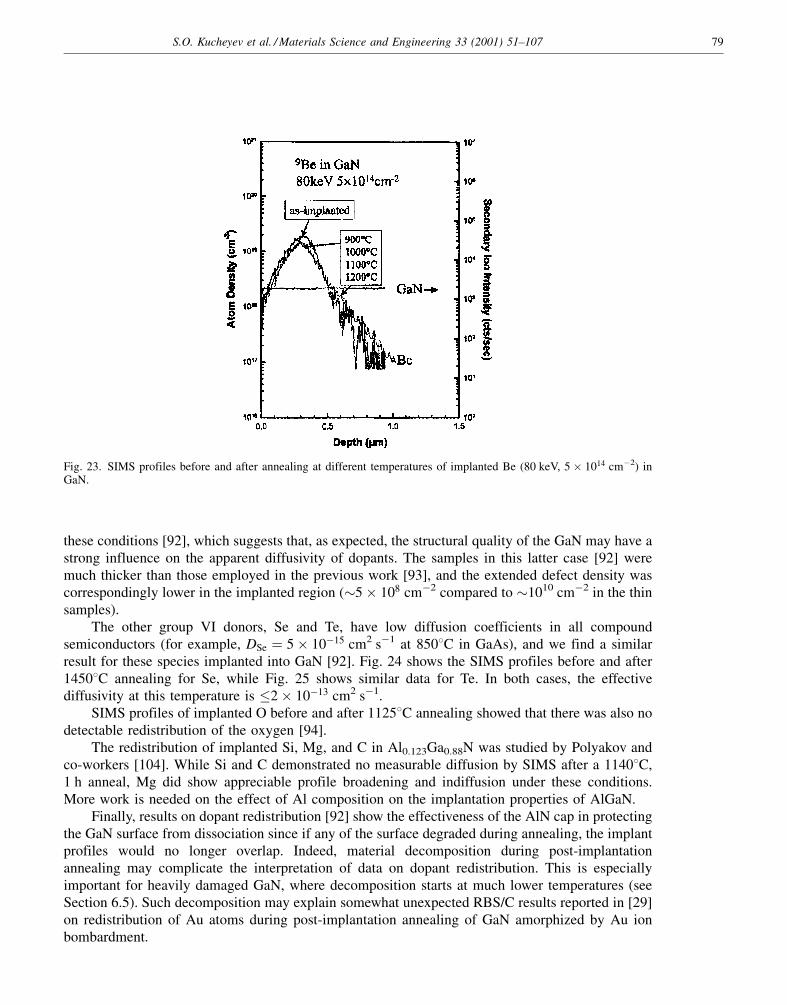
Fig. 23 shows a series of profiles for 9Be before and after annealing up to 12008C. Note thatthere is an initial broadening of the profile at 9008C, corresponding to an effective diffusivity of�5� 10ÿ13 cm2 sÿ1 at this temperature. However, there is no subsequent redistribution attemperatures up to 12008C. Implanted Be shows several types of anomalous diffusion in GaAs,including up-hill diffusion and movement in the tail of the profile, in addition to normalconcentration-dependent diffusion [100], which also results from the non-equilibrium concentrationsof point defects created by the nuclear stopping process of the implanted ions. It appears that in GaN,interstitial Be undergoes a type of transient-enhanced diffusion until these excess point defects areremoved by annealing, at which stage the Be is basically immobile.
Carbon is typically a very slow diffuser in all III±V compounds, since it strongly preferssubstitutional lattice sites [1,98±102]. In GaN, it has been shown that it is possible to get p-typeconductivity in carbon-doped material, albeit with low hole concentrations. In general, however,GaN containing high concentrations of carbon is self-compensated [1], suggesting that carbon isoccupying both Ga and N sites. It is an extremely slow diffuser when implanted into GaN, withDeff � 2� 10ÿ13 cm sÿ1 at 14008C [92].
Similar data for Ca implants in GaN showed that once again there was no detectable motion ofthe acceptor dopant.
Little work has been performed on the diffusion of group VI donors in GaN, although Feng et al.[103] showed that Se displayed relatively high diffusion during growth by metalorganic chemicalvaper deposition (MOCVD) at 10008C. Wilson et al. reported some redistribution of implanted Safter annealing at 700±10008C in relatively thin layers of GaN [93], which might have beeninfluenced by a high defect density in this material. However, more recent SIMS profiles before andafter 14508C annealing of S in GaN have shown that there is clearly no motion of the sulfur under
78 S.O. Kucheyev et al. / Materials Science and Engineering 33 (2001) 51±107
these conditions [92], which suggests that, as expected, the structural quality of the GaN may have astrong influence on the apparent diffusivity of dopants. The samples in this latter case [92] weremuch thicker than those employed in the previous work [93], and the extended defect density wascorrespondingly lower in the implanted region (�5� 108 cmÿ2 compared to �1010 cmÿ2 in the thinsamples).
The other group VI donors, Se and Te, have low diffusion coefficients in all compoundsemiconductors (for example, DSe � 5� 10ÿ15 cm2 sÿ1 at 8508C in GaAs), and we find a similarresult for these species implanted into GaN [92]. Fig. 24 shows the SIMS profiles before and after14508C annealing for Se, while Fig. 25 shows similar data for Te. In both cases, the effectivediffusivity at this temperature is �2� 10ÿ13 cm2 sÿ1.
SIMS profiles of implanted O before and after 11258C annealing showed that there was also nodetectable redistribution of the oxygen [94].
The redistribution of implanted Si, Mg, and C in Al0.123Ga0.88N was studied by Polyakov andco-workers [104]. While Si and C demonstrated no measurable diffusion by SIMS after a 11408C,1 h anneal, Mg did show appreciable profile broadening and indiffusion under these conditions.More work is needed on the effect of Al composition on the implantation properties of AlGaN.
Finally, results on dopant redistribution [92] show the effectiveness of the AlN cap in protectingthe GaN surface from dissociation since if any of the surface degraded during annealing, the implantprofiles would no longer overlap. Indeed, material decomposition during post-implantationannealing may complicate the interpretation of data on dopant redistribution. This is especiallyimportant for heavily damaged GaN, where decomposition starts at much lower temperatures (seeSection 6.5). Such decomposition may explain somewhat unexpected RBS/C results reported in [29]on redistribution of Au atoms during post-implantation annealing of GaN amorphized by Au ionbombardment.
Fig. 23. SIMS profiles before and after annealing at different temperatures of implanted Be (80 keV, 5� 1014 cmÿ2) inGaN.
S.O. Kucheyev et al. / Materials Science and Engineering 33 (2001) 51±107 79

In summary, negligible redistribution has been observed by SIMS for most potential dopants(Be, C, Mg, Si, and Ca) during post-implantation annealing at even 14508C [92]. This bodes well forthe fabrication of GaN-based power devices such as thyristors and insulated gate bipolar transistors,which will require creation of a doped well in source/drain regions by ion implantation. The low
Fig. 24. SIMS profiles before and after annealing at 14508C of implanted Se (300 keV, 5� 1014 cmÿ2) in GaN. Theprofiles are essentially coincident.
Fig. 25. SIMS profiles before and after annealing at 14508C of implanted Te (600 keV, 5� 1014 cmÿ2) in GaN. Theprofiles are essentially coincident.
80 S.O. Kucheyev et al. / Materials Science and Engineering 33 (2001) 51±107

diffusivities of implanted dopants in GaN means that junction placement should be quite precise, andthere will be fewer problems with lateral diffusion of the source/drain regions toward the gate.
6.4. Lattice sites of dopants
The electronic structure of dopants in GaN depends on their position in the lattice. Despite theclear importance of dopant lattice sites for electrical and optical applications, only a few such studieshave been reported in the literature [21,71±75,78,105], as was reviewed elsewhere [1,5]. Here, webriefly summarize the main results on the lattice sites of dopants in GaN.
It has been shown that a relatively high fraction of implanted Si, Ca, Te, and Er atoms issubstitutional even just after implantation [21,71,73,74]. This result is consistent with very efficientdynamic annealing processes in GaN. Indeed, migration and annihilation of ion-beam-generateddefects during ion bombardment are expected to promote the migration of implanted species intoenergetically favorable lattice sites (i.e. substitutional sites in the case of above species). Data from[73,74] suggests that after annealing at 11008C, most of implanted Si or Ca atoms occupy Ga sites.
Several reports have also been published on the lattice location of rare-earth elements implantedinto GaN [71,75,105]. It has been shown that both Er and Pr are thermally stable on substitutional Gasites.
6.5. Recrystallization of amorphous layers
Only a few reports have been published on the annealing behavior of amorphous layers in GaN[15,21,29,36,38,88,89]. Results from [21,38,88] have shown that thermal annealing of amorphousGaN at temperatures above �5008C results in polycrystallization, rather than in solid phase epitaxialgrowth (SPEG). For example, shown in Fig. 26 is an XTEM image showing polycrystallites formedin two amorphous layers (surface and buried amorphous layers) in GaN annealed at 5008C for �2 hin vacuum. These amorphous layers were prepared by implantation with 0.9 and 0.45 MeV Au ions.
Fig. 26. A dark-field XTEM image showing polycrystallites formed in two amorphous layers (surface and buriedamorphous layers) in GaN annealed at 5008C for �2 h in vacuum. These amorphous layers were prepared by implantationwith 0.9 and 0.45 MeV Au ions.
S.O. Kucheyev et al. / Materials Science and Engineering 33 (2001) 51±107 81
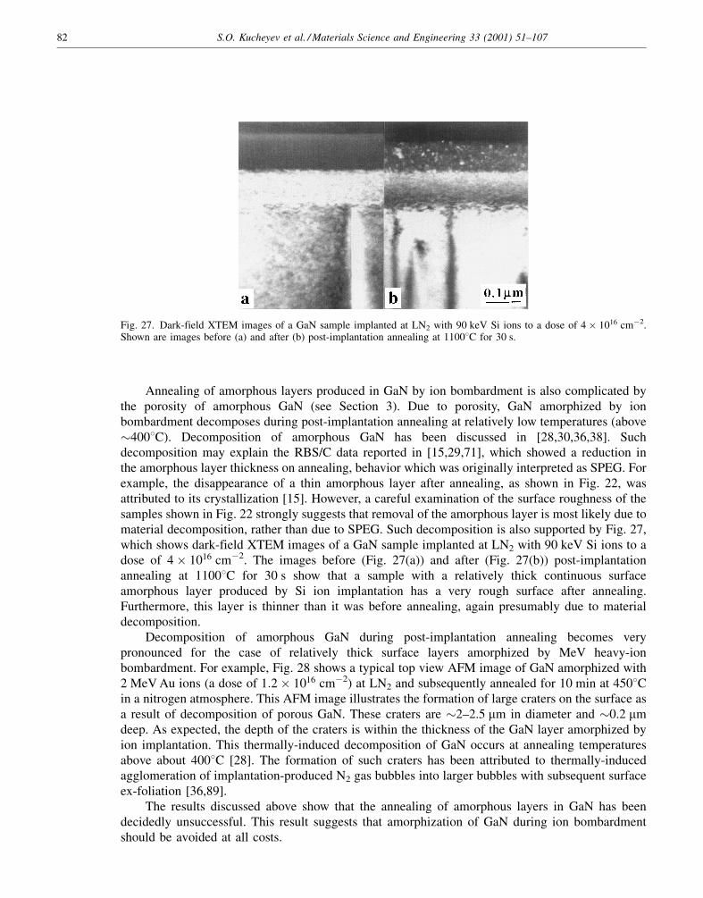
Annealing of amorphous layers produced in GaN by ion bombardment is also complicated bythe porosity of amorphous GaN (see Section 3). Due to porosity, GaN amorphized by ionbombardment decomposes during post-implantation annealing at relatively low temperatures (above�4008C). Decomposition of amorphous GaN has been discussed in [28,30,36,38]. Suchdecomposition may explain the RBS/C data reported in [15,29,71], which showed a reduction inthe amorphous layer thickness on annealing, behavior which was originally interpreted as SPEG. Forexample, the disappearance of a thin amorphous layer after annealing, as shown in Fig. 22, wasattributed to its crystallization [15]. However, a careful examination of the surface roughness of thesamples shown in Fig. 22 strongly suggests that removal of the amorphous layer is most likely due tomaterial decomposition, rather than due to SPEG. Such decomposition is also supported by Fig. 27,which shows dark-field XTEM images of a GaN sample implanted at LN2 with 90 keV Si ions to adose of 4� 1016 cmÿ2. The images before (Fig. 27(a)) and after (Fig. 27(b)) post-implantationannealing at 11008C for 30 s show that a sample with a relatively thick continuous surfaceamorphous layer produced by Si ion implantation has a very rough surface after annealing.Furthermore, this layer is thinner than it was before annealing, again presumably due to materialdecomposition.
Decomposition of amorphous GaN during post-implantation annealing becomes verypronounced for the case of relatively thick surface layers amorphized by MeV heavy-ionbombardment. For example, Fig. 28 shows a typical top view AFM image of GaN amorphized with2 MeV Au ions (a dose of 1:2� 1016 cmÿ2) at LN2 and subsequently annealed for 10 min at 4508Cin a nitrogen atmosphere. This AFM image illustrates the formation of large craters on the surface asa result of decomposition of porous GaN. These craters are �2±2.5 mm in diameter and �0.2 mmdeep. As expected, the depth of the craters is within the thickness of the GaN layer amorphized byion implantation. This thermally-induced decomposition of GaN occurs at annealing temperaturesabove about 4008C [28]. The formation of such craters has been attributed to thermally-inducedagglomeration of implantation-produced N2 gas bubbles into larger bubbles with subsequent surfaceex-foliation [36,89].
The results discussed above show that the annealing of amorphous layers in GaN has beendecidedly unsuccessful. This result suggests that amorphization of GaN during ion bombardmentshould be avoided at all costs.
Fig. 27. Dark-field XTEM images of a GaN sample implanted at LN2 with 90 keV Si ions to a dose of 4� 1016 cmÿ2.Shown are images before (a) and after (b) post-implantation annealing at 11008C for 30 s.
82 S.O. Kucheyev et al. / Materials Science and Engineering 33 (2001) 51±107
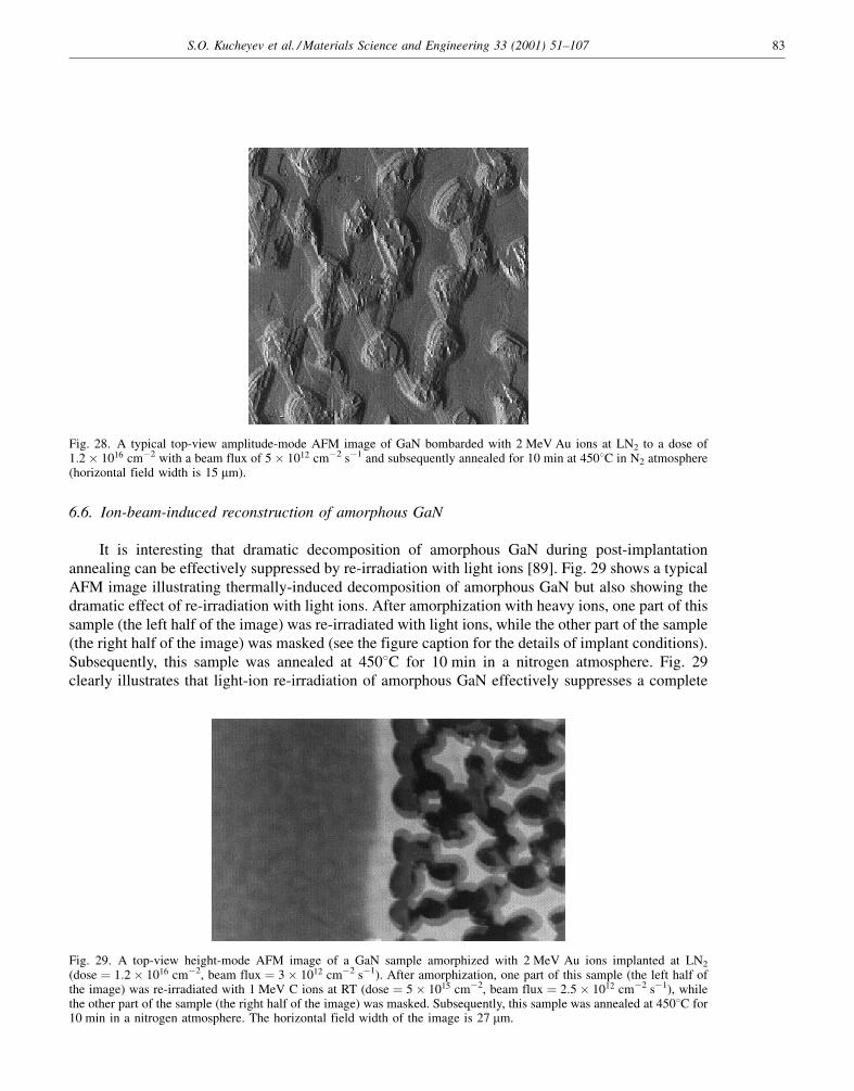
6.6. Ion-beam-induced reconstruction of amorphous GaN
It is interesting that dramatic decomposition of amorphous GaN during post-implantationannealing can be effectively suppressed by re-irradiation with light ions [89]. Fig. 29 shows a typicalAFM image illustrating thermally-induced decomposition of amorphous GaN but also showing thedramatic effect of re-irradiation with light ions. After amorphization with heavy ions, one part of thissample (the left half of the image) was re-irradiated with light ions, while the other part of the sample(the right half of the image) was masked (see the figure caption for the details of implant conditions).Subsequently, this sample was annealed at 4508C for 10 min in a nitrogen atmosphere. Fig. 29clearly illustrates that light-ion re-irradiation of amorphous GaN effectively suppresses a complete
Fig. 28. A typical top-view amplitude-mode AFM image of GaN bombarded with 2 MeV Au ions at LN2 to a dose of1:2� 1016 cmÿ2 with a beam flux of 5� 1012 cmÿ2 sÿ1 and subsequently annealed for 10 min at 4508C in N2 atmosphere(horizontal field width is 15 mm).
Fig. 29. A top-view height-mode AFM image of a GaN sample amorphized with 2 MeV Au ions implanted at LN2
(dose � 1:2� 1016 cmÿ2, beam flux � 3� 1012 cmÿ2 sÿ1). After amorphization, one part of this sample (the left half ofthe image) was re-irradiated with 1 MeV C ions at RT (dose � 5� 1015 cmÿ2, beam flux � 2:5� 1012 cmÿ2 sÿ1), whilethe other part of the sample (the right half of the image) was masked. Subsequently, this sample was annealed at 4508C for10 min in a nitrogen atmosphere. The horizontal field width of the image is 27 mm.
S.O. Kucheyev et al. / Materials Science and Engineering 33 (2001) 51±107 83
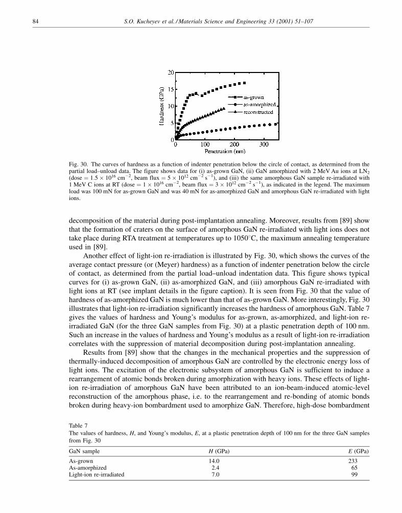
decomposition of the material during post-implantation annealing. Moreover, results from [89] showthat the formation of craters on the surface of amorphous GaN re-irradiated with light ions does nottake place during RTA treatment at temperatures up to 10508C, the maximum annealing temperatureused in [89].
Another effect of light-ion re-irradiation is illustrated by Fig. 30, which shows the curves of theaverage contact pressure (or (Meyer) hardness) as a function of indenter penetration below the circleof contact, as determined from the partial load±unload indentation data. This figure shows typicalcurves for (i) as-grown GaN, (ii) as-amorphized GaN, and (iii) amorphous GaN re-irradiated withlight ions at RT (see implant details in the figure caption). It is seen from Fig. 30 that the value ofhardness of as-amorphized GaN is much lower than that of as-grown GaN. More interestingly, Fig. 30illustrates that light-ion re-irradiation significantly increases the hardness of amorphous GaN. Table 7gives the values of hardness and Young's modulus for as-grown, as-amorphized, and light-ion re-irradiated GaN (for the three GaN samples from Fig. 30) at a plastic penetration depth of 100 nm.Such an increase in the values of hardness and Young's modulus as a result of light-ion re-irradiationcorrelates with the suppression of material decomposition during post-implantation annealing.
Results from [89] show that the changes in the mechanical properties and the suppression ofthermally-induced decomposition of amorphous GaN are controlled by the electronic energy loss oflight ions. The excitation of the electronic subsystem of amorphous GaN is sufficient to induce arearrangement of atomic bonds broken during amorphization with heavy ions. These effects of light-ion re-irradiation of amorphous GaN have been attributed to an ion-beam-induced atomic-levelreconstruction of the amorphous phase, i.e. to the rearrangement and re-bonding of atomic bondsbroken during heavy-ion bombardment used to amorphize GaN. Therefore, high-dose bombardment
Fig. 30. The curves of hardness as a function of indenter penetration below the circle of contact, as determined from thepartial load±unload data. The figure shows data for (i) as-grown GaN, (ii) GaN amorphized with 2 MeV Au ions at LN2
(dose � 1:5� 1016 cmÿ2, beam flux � 5� 1012 cmÿ2 sÿ1), and (iii) the same amorphous GaN sample re-irradiated with1 MeV C ions at RT (dose � 1� 1016 cmÿ2, beam flux � 3� 1012 cmÿ2 sÿ1), as indicated in the legend. The maximumload was 100 mN for as-grown GaN and was 40 mN for as-amorphized GaN and amorphous GaN re-irradiated with lightions.
Table 7
The values of hardness, H, and Young's modulus, E, at a plastic penetration depth of 100 nm for the three GaN samples
from Fig. 30
GaN sample H (GPa) E (GPa)
As-grown 14.0 233As-amorphized 2.4 65Light-ion re-irradiated 7.0 99
84 S.O. Kucheyev et al. / Materials Science and Engineering 33 (2001) 51±107

of GaN with heavy ions (like 197Au), which generate very dense collision cascades, produces ametastable amorphous phase of GaN. This amorphous phase can be further reconstructed bybombardment with lighter ions, when ion-generated collision cascades are dilute.
7. Optical properties
The optical properties of GaN have received extensive attention due to their importance in thefabrication of GaN-based optoelectronic devices. One way to modify the optical characteristics ofGaN is by the introduction of optically-active impurities (such as rare-earth elements) by ionimplantation. Ion implantation has a twofold effect on the optical characteristics of GaN, byintroducing lattice defects as well as optically active impurities. The effects of implantation-produced lattice defects on the optical characteristics of GaN are particularly important tounderstand if applications are to be exploited.
Most of the luminescence studies of ion implanted GaN reported in the literature have beendirected towards three main purposes.
1. To study the effects of ion-beam-produced lattice defects on luminescence (i.e. appearance of newluminescent peaks due to defects or quenching of the characteristic luminescence peaks exhibitedby as-grown GaN due to the introduction of competitive recombination centers).
2. To study the effects of implanted species (such as potential contaminants or rare-earth elements).3. To monitor recovery of ion-beam-produced damage by post-implantation annealing.
Below, we discuss mainly the influence of implantation damage on the luminescence of GaN,which has been studied in [1±5,16,17,20,23,30,68±70,76,79±83,85±87,106±110]. We will not discussrare-earth doping of GaN by ion implantation because this subject has been reviewed in detailelsewhere [1,5].
7.1. The effect of implantation disorder on light absorption
Implantation-produced damage significantly changes the absorption of visible light in GaN.Indeed, as-implanted GaN grown on sapphire undergoes color changes from yellowish-brown toblack, depending on ion dose or the amount of implantation-produced damage. This fact suggeststhat implantation-induced defects act as strong absorbers of light in the blue part of the visiblespectrum. Silkowski et al. [83] studied the RT absorption edge of GaN bombarded with 390 keV Arions to a dose of 5� 1015 cmÿ2 and subsequently annealed at temperatures from 800 to 10508C inflowing NH3 or N2 gas. Their data has shown that implantation damage results in an exponential tailof states near the band-edge. It is surprising that, despite the importance of this problem, moredetailed studies of the influence of implantation-produced defects on light absorption have not beencarried out.
7.2. Quenching of luminescence by ion implantation
All photoluminescence (PL) and cathodoluminescence (CL) data from ion implanted GaNshows that implantation-produced lattice defects act as effective non-radiative recombination centersin GaN, resulting in a severe quenching of most characteristic luminescence peaks exhibited by as-grown GaN. For example, Fig. 31(a) shows CL spectra obtained at RT from virgin and implantedregions of GaN bombarded with 150 keV C ions at LN2 to a dose of 1� 1014 cmÿ2. The spectra
S.O. Kucheyev et al. / Materials Science and Engineering 33 (2001) 51±107 85
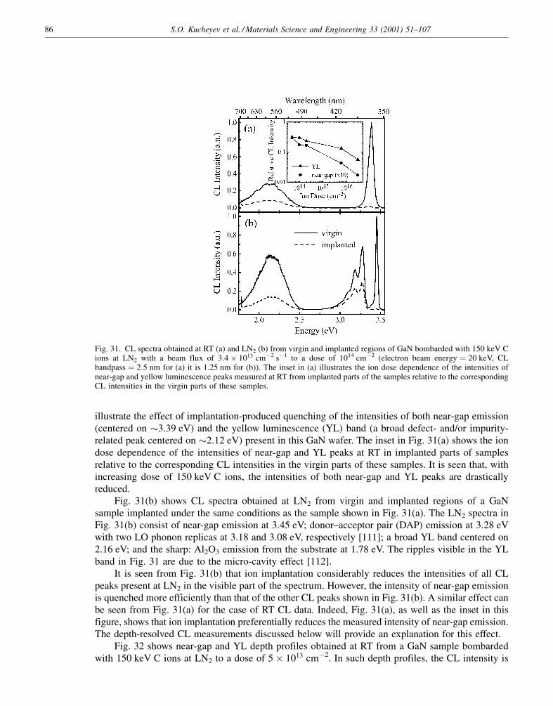
illustrate the effect of implantation-produced quenching of the intensities of both near-gap emission(centered on �3.39 eV) and the yellow luminescence (YL) band (a broad defect- and/or impurity-related peak centered on �2.12 eV) present in this GaN wafer. The inset in Fig. 31(a) shows the iondose dependence of the intensities of near-gap and YL peaks at RT in implanted parts of samplesrelative to the corresponding CL intensities in the virgin parts of these samples. It is seen that, withincreasing dose of 150 keV C ions, the intensities of both near-gap and YL peaks are drasticallyreduced.
Fig. 31(b) shows CL spectra obtained at LN2 from virgin and implanted regions of a GaNsample implanted under the same conditions as the sample shown in Fig. 31(a). The LN2 spectra inFig. 31(b) consist of near-gap emission at 3.45 eV; donor±acceptor pair (DAP) emission at 3.28 eVwith two LO phonon replicas at 3.18 and 3.08 eV, respectively [111]; a broad YL band centered on2.16 eV; and the sharp: Al2O3 emission from the substrate at 1.78 eV. The ripples visible in the YLband in Fig. 31 are due to the micro-cavity effect [112].
It is seen from Fig. 31(b) that ion implantation considerably reduces the intensities of all CLpeaks present at LN2 in the visible part of the spectrum. However, the intensity of near-gap emissionis quenched more efficiently than that of the other CL peaks shown in Fig. 31(b). A similar effect canbe seen from Fig. 31(a) for the case of RT CL data. Indeed, Fig. 31(a), as well as the inset in thisfigure, shows that ion implantation preferentially reduces the measured intensity of near-gap emission.The depth-resolved CL measurements discussed below will provide an explanation for this effect.
Fig. 32 shows near-gap and YL depth profiles obtained at RT from a GaN sample bombardedwith 150 keV C ions at LN2 to a dose of 5� 1013 cmÿ2. In such depth profiles, the CL intensity is
Fig. 31. CL spectra obtained at RT (a) and LN2 (b) from virgin and implanted regions of GaN bombarded with 150 keV Cions at LN2 with a beam flux of 3:4� 1013 cmÿ2 sÿ1 to a dose of 1014 cmÿ2 (electron beam energy � 20 keV, CLbandpass � 2:5 nm for (a) it is 1.25 nm for (b)). The inset in (a) illustrates the ion dose dependence of the intensities ofnear-gap and yellow luminescence peaks measured at RT from implanted parts of the samples relative to the correspondingCL intensities in the virgin parts of these samples.
86 S.O. Kucheyev et al. / Materials Science and Engineering 33 (2001) 51±107

plotted as a function of electron beam energy or the corresponding electron penetration range, RKO,which can be approximated using the Kanaya±Okayama equation [113].
Fig. 32(a) shows that, in the ion-damaged layer (up to �700 nm from the surface), theintensities of both near-gap and YL peaks are drastically reduced below the detectable level.Therefore, CL emission from the implanted sample shown in Fig. 31, obtained with an electron beamenergy of 20 keV, is actually generated by the electron beam impinging on virgin GaN, beyond theimplanted layer8. This observation can be used to explain the preferential quenching of near-gapemission compared with the other emission peaks in Fig. 31. Indeed, it has been shown [114] thatself-absorption can change detected CL near-gap emission of as-grown GaN. Results from [91] alsoindicate that implantation-induced absorption of CL in the implanted layer can strongly affectdetected near-gap emission from underlying virgin GaN. Note that, in as-grown GaN, the measuredintensity of near-gap emission decreases with increasing electron beam energy due to efficient self-absorption, and the YL intensity increases with beam energy due to a corresponding increase in theconcentration of YL centers towards the GaN/sapphire interface (see for example, [114]) and/or dueto the saturation of YL emission.
As has been reported by several groups (see for example [23,70,79,80,83,85]), the annealing ofGaN implanted with keV ions usually recovers (although always only partly) the measuredintensities of light emission. Such partial recovery of luminescence intensity is generally attributed
Fig. 32. Near-gap and yellow luminescence (YL) depth profiles obtained at RT from a GaN sample bombarded with150 keV C ions at LN2 with a beam flux of 3:4� 1013 cmÿ2 sÿ1 to a dose of 5� 1013 cmÿ2 (CL bandpass � 25 nm,electron beam power � 7 mW). Shown are the depth profiles of the implanted GaN sample before (a) and after (b) post-implantation annealing at 10508C for 15 s.
8 Note that the sample shown in Fig. 28 was bombarded to twice the dose (1� 1014 cmÿ2) of the sample shown in Fig. 29
(5� 1013 cmÿ2). Therefore, the effect of the quenching of CL emission coming from the implanted layer is even more
pronounced in Fig. 28.
S.O. Kucheyev et al. / Materials Science and Engineering 33 (2001) 51±107 87

to a corresponding partial recovery of non-radiative defects produced by ion bombardment.However, as reported in [90], implantation-produced damage and post-implantation annealing affectnot only light emission from the implanted layer but also the detection of CL emission from virginGaN due to the absorption of light within the implanted layer. Awareness of this behavior is requiredfor a correct interpretation of luminescence measurements of GaN optically doped by implantationwith keV ions.
Shown in Fig. 32(b) are CL depth profiles taken from the same sample shown in Fig. 32(a) afterannealing at 10508C for 15 s. It is seen that such an annealing does not recover either near-gap or YLemission generated in the near-surface region (up to �450 nm from the surface). This depth isconsistent with TRIM calculations [11], which indicate that the layer directly modified bybombardment with 150 keV C ions (say, Rp � 3DRp, where Rp is the projected ion range, and DRp isthe ion straggling) is also �450 nm thick. Therefore, the apparent recovery of emission by such anannealing9 can be attributed to the thermal recovery of damage that enhances the absorption of lightwithin the implanted layer. This conclusion is consistent with changes in the color of implantedsamples observed to result from annealing [90]. Results from [90] have shown that the (partial)recovery of CL emission in the implanted layer by annealing at temperatures up to 10508C occursonly for rather low dose implantation with 150 keV C ions (doses of �1012 cmÿ2).
Another interesting result from Fig. 32(a) is that, in as-implanted GaN, the CL is quenched up toa depth of �700 mm, which is well beyond the layer modified by ion bombardment, as given byTRIM [11], which takes into account only collisional processes. Such quenching of CL emissionbeyond the ion penetration range can be attributed to the diffusion of implantation-produced pointdefects. This conclusion is supported by the fact that ion-generated point defects are highly mobile inGaN at LN2 and above. Fig. 32(b) also shows that the defect complexes formed by such mobile pointdefects can be effectively removed by annealing at 10508C.
The conclusion that CL of GaN is dramatically quenched by relatively low dose ionbombardment is consistent with the results of luminescence studies of GaN irradiated with MeVlight ions [30,115]. An analysis of CL spectra from GaN implanted with 150 keV C or 1.8 MeV Heions at RT has shown that disorder produced by light-ion bombardment to a critical dosecorresponding to the generation of �5� 1019 vacancies per centimetercube is sufficient to reducethe intensity of near-gap emission by more than two orders of magnitude [90]. However, the exactvalue of this critical dose depends on a number of implant parameters, such as ion mass, energy,beam flux, and substrate temperature [115].
7.3. New luminescence peaks
It can be concluded that implantation-produced lattice defects themselves (both before andafter post-implantation annealing of GaN) do not give rise to any luminescence peaks in the visiblepart of the spectrum. Although, the first reports on PL of ion implanted GaN suggested thatimplantation disorder was responsible for YL in GaN [79,80,116], this conclusion has not beensupported by later experiments. Indeed, luminescence data from more recent reports suggests thatYL originates from a defect-impurity complex [83,85,115]. The impurities which are responsiblefor YL are still unknown, although some results support carbon and oxygen as plausible candidates[83,115±117].
9 After such an annealing of the sample from Fig. 32, the relative intensity of near-gap emission (measured with an
electron beam energy of 20 keV) in the implanted part to that in the virgin part of the sample recovered from �4% in the
as-implanted sample to �14% in the annealed one.
88 S.O. Kucheyev et al. / Materials Science and Engineering 33 (2001) 51±107
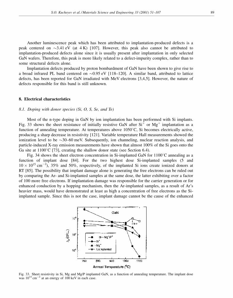
Another luminescence peak which has been attributed to implantation-produced defects is apeak centered on �3.41 eV (at 4 K) [107]. However, this peak also cannot be attributed toimplantation-produced defects alone since it is usually present after implantation in only selectedGaN wafers. Therefore, this peak is more likely related to a defect-impurity complex, rather than tosome structural defects alone.
Implantation defects produced by proton bombardment of GaN have been shown to give rise toa broad infrared PL band centered on �0.95 eV [118±120]. A similar band, attributed to latticedefects, has been reported for GaN irradiated with MeV electrons [3,4,5]. However, the nature ofdefects responsible for this band is still unknown.
8. Electrical characteristics
8.1. Doping with donor species (Si, O, S, Se, and Te)
Most of the n-type doping in GaN by ion implantation has been performed with Si implants.Fig. 33 shows the sheet resistance of initially resistive GaN after Si� or Mg� implantation as afunction of annealing temperature. At temperatures above 10508C, Si becomes electrically active,producing a sharp decrease in resistivity [121]. Variable temperature Hall measurements showed theionization level to be �30±60 meV. Subsequently, ion channeling, nuclear reaction analysis, andparticle-induced X-ray emission measurements have shown that almost 100% of the Si goes onto theGa site at 11008C [73], creating the shallow donor state (see Section 6.4).
Fig. 34 shows the sheet electron concentration in Si-implanted GaN for 11008C annealing as afunction of implant dose [84]. For the two highest dose Si-implanted samples (5 and10� 1015 cmÿ2), 35% and 50%, respectively, of the implanted Si ions create ionized donors atRT [85]. The possibility that implant damage alone is generating the free electrons can be ruled outby comparing the Ar- and Si-implanted samples at the same dose, the latter exhibiting over a factorof 100 more free electrons. If implantation damage was responsible for the carrier generation or forenhanced conduction by a hopping mechanism, then the Ar-implanted samples, as a result of Ar'sheavier mass, would have demonstrated at least as high a concentration of free electrons as the Si-implanted sample. Since this is not the case, implant damage cannot be the cause of the enhanced
Fig. 33. Sheet resistivity in Si, Mg and Mg/P implanted GaN, as a function of annealing temperature. The implant dosewas 1014 cmÿ2 at an energy of 100 keV in each case.
S.O. Kucheyev et al. / Materials Science and Engineering 33 (2001) 51±107 89
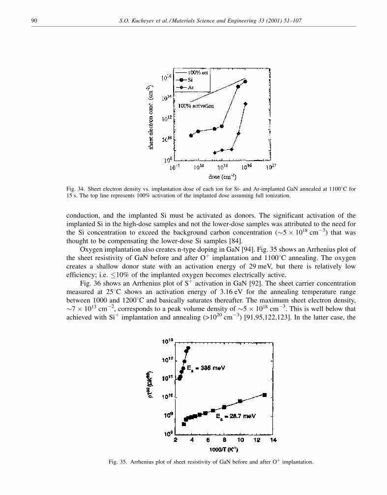
conduction, and the implanted Si must be activated as donors. The significant activation of theimplanted Si in the high-dose samples and not the lower-dose samples was attributed to the need forthe Si concentration to exceed the background carbon concentration (�5� 1018 cmÿ3) that wasthought to be compensating the lower-dose Si samples [84].
Oxygen implantation also creates n-type doping in GaN [94]. Fig. 35 shows an Arrhenius plot ofthe sheet resistivity of GaN before and after O� implantation and 11008C annealing. The oxygencreates a shallow donor state with an activation energy of 29 meV, but there is relatively lowefficiency; i.e. �10% of the implanted oxygen becomes electrically active.
Fig. 36 shows an Arrhenius plot of S� activation in GaN [92]. The sheet carrier concentrationmeasured at 258C shows an activation energy of 3.16 eV for the annealing temperature rangebetween 1000 and 12008C and basically saturates thereafter. The maximum sheet electron density,�7� 1013 cmÿ2, corresponds to a peak volume density of �5� 1018 cmÿ3. This is well below thatachieved with Si� implantation and annealing (>1020 cmÿ3) [91,95,122,123]. In the latter case, the
Fig. 34. Sheet electron density vs. implantation dose of each ion for Si- and Ar-implanted GaN annealed at 11008C for15 s. The top line represents 100% activation of the implanted dose assuming full ionization.
Fig. 35. Arrhenius plot of sheet resistivity of GaN before and after O� implantation.
90 S.O. Kucheyev et al. / Materials Science and Engineering 33 (2001) 51±107

carrier density showed an activation energy of 5.2 eV. The physical origin of this activation energycontains several components Ð basically it is the energy required to move an implanted ion onto asubstitutional lattice site and for it to show electrical activity. This latter requirement means thatcompensating defects must also be annealed out. Even though implanted Si at the same dose showedevidence of site switching and self-compensation [95], it still produces a higher peak doping levelthan the non-amphoteric donor S, which is only slightly heavier (32S versus 28Si). From temperature-dependent Hall measurements, we find a S� donor ionization level of 48� 10 meV, so that thedonors are fully ionized at RT [92].
Similar data is shown in Fig. 37 for Te� implantation. The activation starts around the sametemperature as for S, but much lower sheet electron densities are obtained, the activation energy is
Fig. 36. Arrhenius plot of sheet electron density in S�-implanted GaN vs. annealing temperature.
Fig. 37. Arrhenius plot of sheet electron density in Te�-implanted GaN vs. annealing temperature.
S.O. Kucheyev et al. / Materials Science and Engineering 33 (2001) 51±107 91
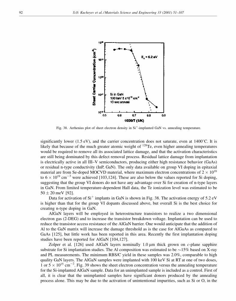
significantly lower (1.5 eV), and the carrier concentration does not saturate, even at 14008C. It islikely that because of the much greater atomic weight of 128Te, even higher annealing temperatureswould be required to remove all its associated lattice damage, and that the activation characteristicsare still being dominated by this defect removal process. Residual lattice damage from implantationis electrically active in all III±V semiconductors, producing either high resistance behavior (GaAs)or residual n-type conductivity (InP, GaN). The only data available on group VI doping in epitaxialmaterial are from Se-doped MOCVD material, where maximum electron concentrations of 2� 1018
to 6� 1019 cmÿ3 were achieved [103,124]. These are also below the values reported for Si doping,suggesting that the group VI donors do not have any advantage over Si for creation of n-type layersin GaN. From limited temperature-dependent Hall data, the Te ionization level was estimated to be50� 20 meV [92].
Data for activation of Si� implants in GaN is shown in Fig. 38. The activation energy of 5.2 eVis higher than that for the group VI dopants discussed above, but overall Si is the best choice forcreating n-type doping in GaN.
AlGaN layers will be employed in heterostructure transistors to realize a two dimensionalelectron gas (2-DEG) and to increase the transistor breakdown voltage. Implantation can be used toreduce the transistor access resistance of the AlGaN barrier. One would anticipate that the addition ofAl to the GaN matrix will increase the damage threshold as is the case for AlGaAs as compared toGaAs [125], but little work has been reported in this area. Recently the first implantation dopingstudies have been reported for AlGaN [104,127].
Zolper et al. [126] used AlGaN layers nominally 1.0 mm thick grown on c-plane sapphiresubstrate for Si implantation studies. The Al composition was estimated to be �15% based on X-rayand PL measurements. The minimum RBS/C yield in these samples was 2.0%, comparable to highquality GaN layers. The AlGaN samples were implanted with 100 keV Si at RT at one of two doses,1 or 5� 1015 cmÿ2. Fig. 39 shows the sheet electron concentration versus the annealing temperaturefor the Si-implanted AlGaN sample. Data for an unimplanted sample is included as a control. First ofall, it is clear that the unimplanted samples have significant donors produced by the annealingprocess alone. This may be due to the activation of unintentional impurities, such as Si or O, in the
Fig. 38. Arrhenius plot of sheet electron density in Si�-implanted GaN vs. annealing temperature.
92 S.O. Kucheyev et al. / Materials Science and Engineering 33 (2001) 51±107
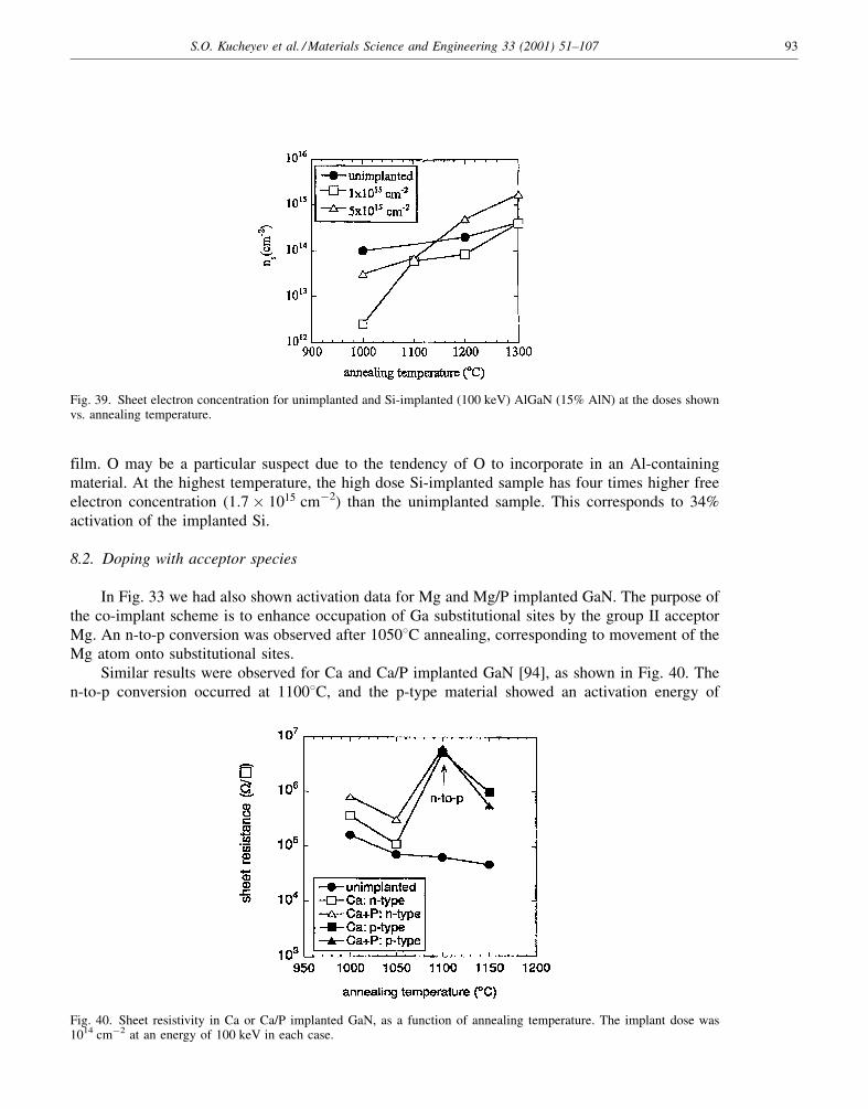
film. O may be a particular suspect due to the tendency of O to incorporate in an Al-containingmaterial. At the highest temperature, the high dose Si-implanted sample has four times higher freeelectron concentration (1:7� 1015 cmÿ2) than the unimplanted sample. This corresponds to 34%activation of the implanted Si.
8.2. Doping with acceptor species
In Fig. 33 we had also shown activation data for Mg and Mg/P implanted GaN. The purpose ofthe co-implant scheme is to enhance occupation of Ga substitutional sites by the group II acceptorMg. An n-to-p conversion was observed after 10508C annealing, corresponding to movement of theMg atom onto substitutional sites.
Similar results were observed for Ca and Ca/P implanted GaN [94], as shown in Fig. 40. Then-to-p conversion occurred at 11008C, and the p-type material showed an activation energy of
Fig. 39. Sheet electron concentration for unimplanted and Si-implanted (100 keV) AlGaN (15% AlN) at the doses shownvs. annealing temperature.
Fig. 40. Sheet resistivity in Ca or Ca/P implanted GaN, as a function of annealing temperature. The implant dose was1014 cmÿ2 at an energy of 100 keV in each case.
S.O. Kucheyev et al. / Materials Science and Engineering 33 (2001) 51±107 93
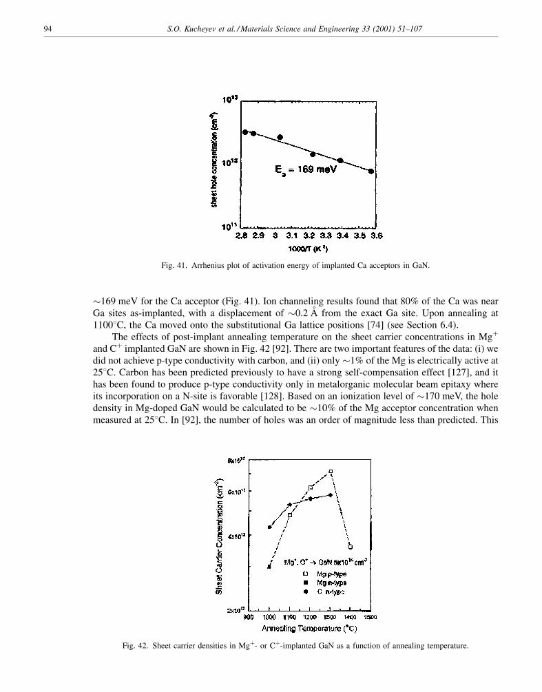
�169 meV for the Ca acceptor (Fig. 41). Ion channeling results found that 80% of the Ca was nearGa sites as-implanted, with a displacement of �0.2 AÊ from the exact Ga site. Upon annealing at11008C, the Ca moved onto the substitutional Ga lattice positions [74] (see Section 6.4).
The effects of post-implant annealing temperature on the sheet carrier concentrations in Mg�
and C� implanted GaN are shown in Fig. 42 [92]. There are two important features of the data: (i) wedid not achieve p-type conductivity with carbon, and (ii) only �1% of the Mg is electrically active at258C. Carbon has been predicted previously to have a strong self-compensation effect [127], and ithas been found to produce p-type conductivity only in metalorganic molecular beam epitaxy whereits incorporation on a N-site is favorable [128]. Based on an ionization level of �170 meV, the holedensity in Mg-doped GaN would be calculated to be �10% of the Mg acceptor concentration whenmeasured at 258C. In [92], the number of holes was an order of magnitude less than predicted. This
Fig. 41. Arrhenius plot of activation energy of implanted Ca acceptors in GaN.
Fig. 42. Sheet carrier densities in Mg�- or C�-implanted GaN as a function of annealing temperature.
94 S.O. Kucheyev et al. / Materials Science and Engineering 33 (2001) 51±107
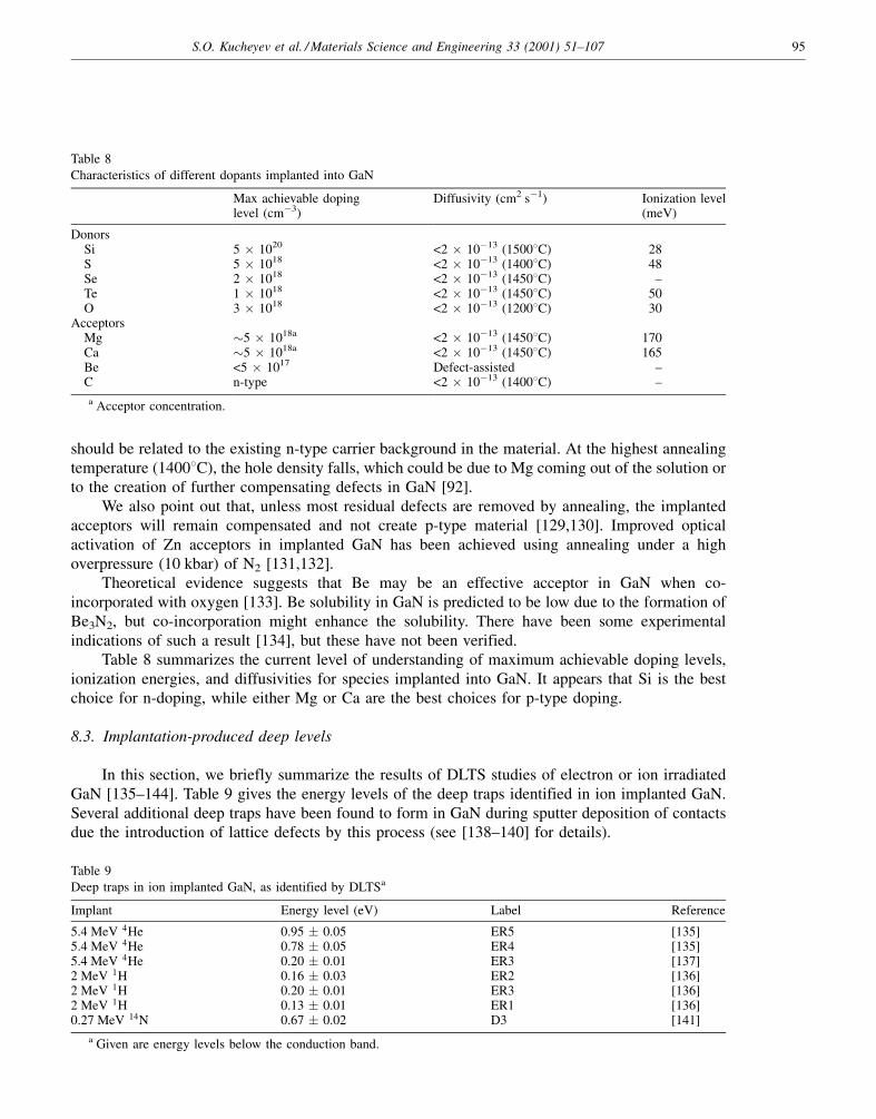
should be related to the existing n-type carrier background in the material. At the highest annealingtemperature (14008C), the hole density falls, which could be due to Mg coming out of the solution orto the creation of further compensating defects in GaN [92].
We also point out that, unless most residual defects are removed by annealing, the implantedacceptors will remain compensated and not create p-type material [129,130]. Improved opticalactivation of Zn acceptors in implanted GaN has been achieved using annealing under a highoverpressure (10 kbar) of N2 [131,132].
Theoretical evidence suggests that Be may be an effective acceptor in GaN when co-incorporated with oxygen [133]. Be solubility in GaN is predicted to be low due to the formation ofBe3N2, but co-incorporation might enhance the solubility. There have been some experimentalindications of such a result [134], but these have not been verified.
Table 8 summarizes the current level of understanding of maximum achievable doping levels,ionization energies, and diffusivities for species implanted into GaN. It appears that Si is the bestchoice for n-doping, while either Mg or Ca are the best choices for p-type doping.
8.3. Implantation-produced deep levels
In this section, we briefly summarize the results of DLTS studies of electron or ion irradiatedGaN [135±144]. Table 9 gives the energy levels of the deep traps identified in ion implanted GaN.Several additional deep traps have been found to form in GaN during sputter deposition of contactsdue the introduction of lattice defects by this process (see [138±140] for details).
Table 8
Characteristics of different dopants implanted into GaN
Max achievable dopinglevel (cmÿ3)
Diffusivity (cm2 sÿ1) Ionization level(meV)
DonorsSi 5 � 1020 <2 � 10ÿ13 (15008C) 28S 5 � 1018 <2 � 10ÿ13 (14008C) 48Se 2 � 1018 <2 � 10ÿ13 (14508C) ±Te 1 � 1018 <2 � 10ÿ13 (14508C) 50O 3 � 1018 <2 � 10ÿ13 (12008C) 30
AcceptorsMg �5 � 1018a <2 � 10ÿ13 (14508C) 170Ca �5 � 1018a <2 � 10ÿ13 (14508C) 165Be <5 � 1017 Defect-assisted ±C n-type <2 � 10ÿ13 (14008C) ±
a Acceptor concentration.
Table 9
Deep traps in ion implanted GaN, as identified by DLTSa
Implant Energy level (eV) Label Reference
5.4 MeV 4He 0.95 � 0.05 ER5 [135]5.4 MeV 4He 0.78 � 0.05 ER4 [135]5.4 MeV 4He 0.20 � 0.01 ER3 [137]2 MeV 1H 0.16 � 0.03 ER2 [136]2 MeV 1H 0.20 � 0.01 ER3 [136]2 MeV 1H 0.13 � 0.01 ER1 [136]0.27 MeV 14N 0.67 � 0.02 D3 [141]
a Given are energy levels below the conduction band.
S.O. Kucheyev et al. / Materials Science and Engineering 33 (2001) 51±107 95

It should also be noted that deep traps identified in DLTS studies discussed here most likelyoriginate from some defect complexes (or impurity-defect complexes) in GaN rather than fromsimple point defects, such as vacancies and interstitials. Indeed, results of a number of recent studies[33,145,146] strongly suggest that ion-produced Frenkel pairs are mobile in GaN at RT.
8.4. Isolation
Implant isolation has been widely used in compound semiconductor devices for inter-deviceisolation such as in transistor circuits or to produce current confinement such as in lasers [147±149].The implantation process can compensate a semiconductor layer either by a damage or chemicalmechanism. For damage compensation, the resistance typically goes through a maximum withincreasing post-implantation annealing temperature as damage is annealed out and hoppingconduction is reduced. At higher temperatures, the defect density is further reduced below thatrequired to compensate the material, and the resistivity decreases. For chemical compensation, thepost-implantation resistance again increases with annealing temperature with a reduction in hoppingconduction but it then stabilizes at higher temperatures as a thermally stable compensating deep levelis formed. Typically, there is a minimum dose (dependent on the doping level of the sample) requiredfor the chemically active isolation species to achieve thermally stable compensation [150].Thermally stable implant isolation has been reported for n- and p-type AlGaAs where an Al±Ocomplex is thought to form [150,151] and for C-doped GaAs and AlGaAs [152]. With thisbackground, the implant isolation properties of the III-N materials are reviewed.
A number of studies of electrical isolation of GaN have been reported in the literature[87,121,153±157]. It has been shown that isolation which withstands thermal annealing attemperatures at least up to 5008C can be readily achieved by irradiation of GaN with keV H, He, N,O, Ti, Cr, or Fe ions. For example, Fig. 43 shows that N-implantation (at doses of 1012±1013 cmÿ3)effectively compensates both p- and n-type GaN [121]. For both doping types, the resistance firstincreases with annealing temperature and then reaches a maximum before demonstrating asignificant reduction after an 8508C anneal for n-type and a 9508C anneal for p-type GaN. Thisbehavior is typical for implant-damage compensation. The defect levels estimated from Arrheniusplots of the resistance/temperature product are 0.83 eV for initially n-type and 0.90 eV for initially
Fig. 43. Sheet resistance vs. annealing temperature for N implanted initially n- and p-type GaN. The N was implanted atmultiple energies to give an approximately uniform ion concentration of 4� 1018 cmÿ3 across �500 nm.
96 S.O. Kucheyev et al. / Materials Science and Engineering 33 (2001) 51±107
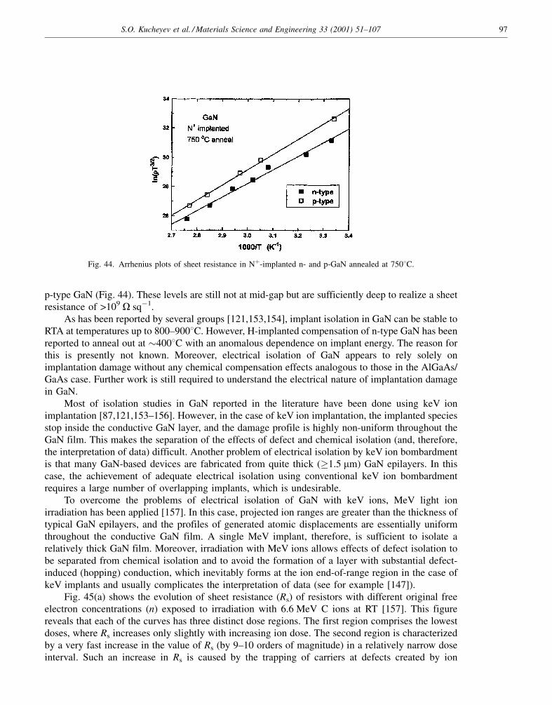
p-type GaN (Fig. 44). These levels are still not at mid-gap but are sufficiently deep to realize a sheetresistance of >109 O sqÿ1.
As has been reported by several groups [121,153,154], implant isolation in GaN can be stable toRTA at temperatures up to 800±9008C. However, H-implanted compensation of n-type GaN has beenreported to anneal out at �4008C with an anomalous dependence on implant energy. The reason forthis is presently not known. Moreover, electrical isolation of GaN appears to rely solely onimplantation damage without any chemical compensation effects analogous to those in the AlGaAs/GaAs case. Further work is still required to understand the electrical nature of implantation damagein GaN.
Most of isolation studies in GaN reported in the literature have been done using keV ionimplantation [87,121,153±156]. However, in the case of keV ion implantation, the implanted speciesstop inside the conductive GaN layer, and the damage profile is highly non-uniform throughout theGaN film. This makes the separation of the effects of defect and chemical isolation (and, therefore,the interpretation of data) difficult. Another problem of electrical isolation by keV ion bombardmentis that many GaN-based devices are fabricated from quite thick (�1.5 mm) GaN epilayers. In thiscase, the achievement of adequate electrical isolation using conventional keV ion bombardmentrequires a large number of overlapping implants, which is undesirable.
To overcome the problems of electrical isolation of GaN with keV ions, MeV light ionirradiation has been applied [157]. In this case, projected ion ranges are greater than the thickness oftypical GaN epilayers, and the profiles of generated atomic displacements are essentially uniformthroughout the conductive GaN film. A single MeV implant, therefore, is sufficient to isolate arelatively thick GaN film. Moreover, irradiation with MeV ions allows effects of defect isolation tobe separated from chemical isolation and to avoid the formation of a layer with substantial defect-induced (hopping) conduction, which inevitably forms at the ion end-of-range region in the case ofkeV implants and usually complicates the interpretation of data (see for example [147]).
Fig. 45(a) shows the evolution of sheet resistance (Rs) of resistors with different original freeelectron concentrations (n) exposed to irradiation with 6.6 MeV C ions at RT [157]. This figurereveals that each of the curves has three distinct dose regions. The first region comprises the lowestdoses, where Rs increases only slightly with increasing ion dose. The second region is characterizedby a very fast increase in the value of Rs (by 9±10 orders of magnitude) in a relatively narrow doseinterval. Such an increase in Rs is caused by the trapping of carriers at defects created by ion
Fig. 44. Arrhenius plots of sheet resistance in N�-implanted n- and p-GaN annealed at 7508C.
S.O. Kucheyev et al. / Materials Science and Engineering 33 (2001) 51±107 97

irradiation and damage-induced degradation of carrier mobility. Fig. 45(a) also shows that, withfurther increasing ion dose, Rs values reach their highest levels after a certain dose has beenaccumulated (Dth: the so-called threshold dose). The third dose region is for ion doses larger thanDth. With increasing ion dose above Dth and up to the maximum doses used in [157], the measuredvalues of Rs remain approximately constant, forming a plateau. The levels of Rs at the plateausshown in Fig. 45 are of the order of 1±2� 1011 O sqÿ1. However, the real maximum values of Rs ofGaN layers are even larger since the Rs values measured have a contribution from the parasiticresistances of the experimental set-up, which are of the same order of magnitude [157].
Fig. 45(a) clearly shows that the dose dependence of Rs is not linear. A similar non-linear dosedependence in GaN has previously been observed and explained by Uzan-Saguy et al. [87] based ona theory of electron transport in doped poly-crystalline materials. However, this non-linearity of Rs asa function of ion dose may be more simply explained. Indeed, in the first approximation, theconcentration of deep traps, created by ion irradiation, linearly increases with dose, and,consequently, n will linearly decrease with ion dose. Therefore, the strong non-linear dosedependence of Rs observed in Fig. 45(a) is not unexpected, taking into account that Rs / 1/n.Moreover, with increasing number of traps in GaN, the concentration of charged scattering centerssignificantly increases, and electron mobility decreases, contributing to strong non-linearity of Rs onion dose. In addition, the real dose dependence of Rs may be more complex. For example, theconcentration of deep traps may not increase linearly with dose due to complex defect interactionand dynamic annealing processes, as discussed in detail in Section 2.
Fig. 45. (a) Dose dependence of sheet resistance of GaN samples irradiated with 6.6 MeV C ions. Samples had differentoriginal free electron concentrations, as indicated in the legend. (b) The original free carrier concentration of the samplesvs. threshold doses obtained from data in (a). The straight line with a slope of 1.0, representing the best fit, is shown.
98 S.O. Kucheyev et al. / Materials Science and Engineering 33 (2001) 51±107
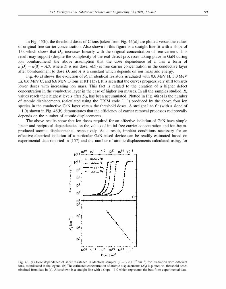
In Fig. 45(b), the threshold doses of C ions [taken from Fig. 45(a)] are plotted versus the valuesof original free carrier concentration. Also shown in this figure is a straight line fit with a slope of1.0, which shows that Dth increases linearly with the original concentration of free carriers. Thisresult may support (despite the complexity of the real defect processes taking place in GaN duringion bombardment) the above assumption that the dose dependence of n has a form ofn�D� � n�0� ÿ AD, where D is ion dose, n(D) is free carrier concentration in the conductive layerafter bombardment to dose D, and A is a constant which depends on ion mass and energy.
Fig. 46(a) shows the evolution of Rs in identical resistors irradiated with 0.6 MeV H, 3.0 MeVLi, 6.6 MeV C, and 6.6 MeV O ions at RT [157]. It is seen that the curves progressively shift towardslower doses with increasing ion mass. This fact is related to the creation of a higher defectconcentration in the conductive layer in the case of higher ion masses. In all the samples studied, Rs
values reach their highest levels after Dth has been accumulated. Plotted in Fig. 46(b) is the numberof atomic displacements (calculated using the TRIM code [11]) produced by the above four ionspecies in the conductive GaN layer versus the threshold doses. A straight line fit (with a slope ofÿ1.0) shown in Fig. 46(b) demonstrates that the efficiency of carrier removal processes reciprocallydepends on the number of atomic displacements.
The above results show that ion doses required for an effective isolation of GaN have simplelinear and reciprocal dependencies on the values of initial free carrier concentration and ion-beam-produced atomic displacements, respectively. As a result, implant conditions necessary for aneffective electrical isolation of a particular GaN-based device can be readily estimated based onexperimental data reported in [157] and the number of atomic displacements calculated using, for
Fig. 46. (a) Dose dependence of sheet resistance in identical samples (n � 3� 1017 cmÿ3) for irradiation with differentions, as indicated in the legend. (b) The estimated concentration of atomic displacements (Nd) is plotted vs. threshold dosesobtained from data in (a). Also shown is a straight line with a slope ÿ1.0 which represents the best fit to experimental data.
S.O. Kucheyev et al. / Materials Science and Engineering 33 (2001) 51±107 99
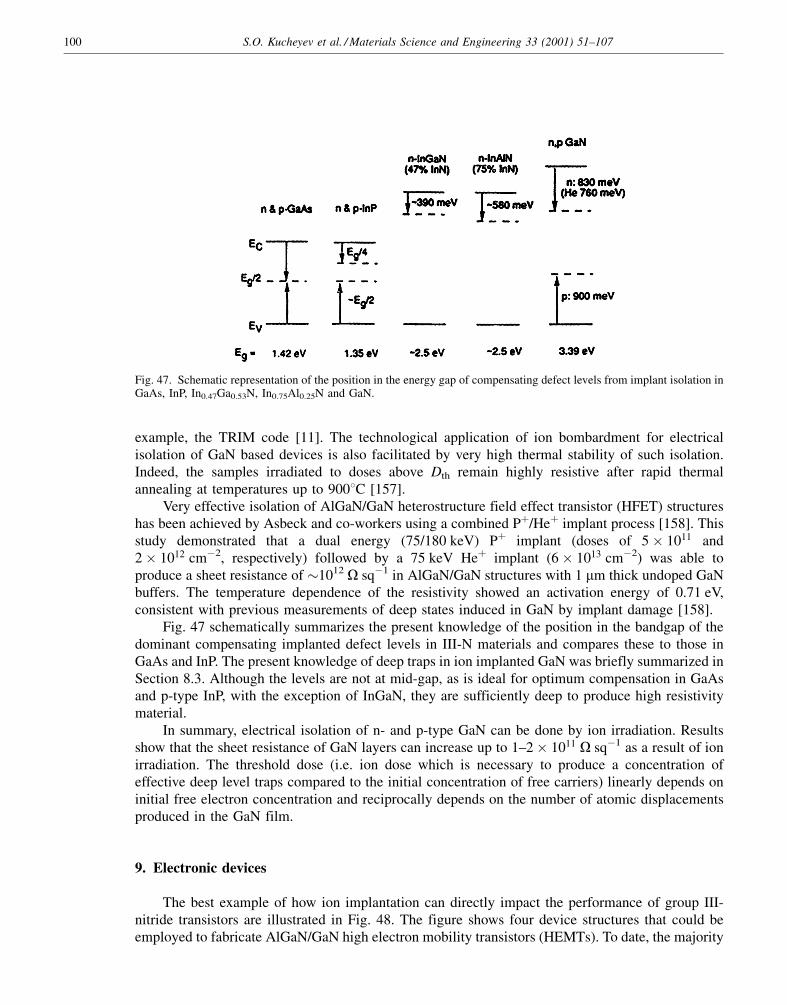
example, the TRIM code [11]. The technological application of ion bombardment for electricalisolation of GaN based devices is also facilitated by very high thermal stability of such isolation.Indeed, the samples irradiated to doses above Dth remain highly resistive after rapid thermalannealing at temperatures up to 9008C [157].
Very effective isolation of AlGaN/GaN heterostructure field effect transistor (HFET) structureshas been achieved by Asbeck and co-workers using a combined P�/He� implant process [158]. Thisstudy demonstrated that a dual energy (75/180 keV) P� implant (doses of 5� 1011 and2� 1012 cmÿ2, respectively) followed by a 75 keV He� implant (6� 1013 cmÿ2) was able toproduce a sheet resistance of �1012 O sqÿ1 in AlGaN/GaN structures with 1 mm thick undoped GaNbuffers. The temperature dependence of the resistivity showed an activation energy of 0.71 eV,consistent with previous measurements of deep states induced in GaN by implant damage [158].
Fig. 47 schematically summarizes the present knowledge of the position in the bandgap of thedominant compensating implanted defect levels in III-N materials and compares these to those inGaAs and InP. The present knowledge of deep traps in ion implanted GaN was briefly summarized inSection 8.3. Although the levels are not at mid-gap, as is ideal for optimum compensation in GaAsand p-type InP, with the exception of InGaN, they are sufficiently deep to produce high resistivitymaterial.
In summary, electrical isolation of n- and p-type GaN can be done by ion irradiation. Resultsshow that the sheet resistance of GaN layers can increase up to 1±2� 1011 O sqÿ1 as a result of ionirradiation. The threshold dose (i.e. ion dose which is necessary to produce a concentration ofeffective deep level traps compared to the initial concentration of free carriers) linearly depends oninitial free electron concentration and reciprocally depends on the number of atomic displacementsproduced in the GaN film.
9. Electronic devices
The best example of how ion implantation can directly impact the performance of group III-nitride transistors are illustrated in Fig. 48. The figure shows four device structures that could beemployed to fabricate AlGaN/GaN high electron mobility transistors (HEMTs). To date, the majority
Fig. 47. Schematic representation of the position in the energy gap of compensating defect levels from implant isolation inGaAs, InP, In0.47Ga0.53N, In0.75Al0.25N and GaN.
100 S.O. Kucheyev et al. / Materials Science and Engineering 33 (2001) 51±107

of the AlGaN/GaN HEMTs transistors have been fabricated in a planar structure as shown inFig. 48(a), where the Ohmic source and drain contacts are placed directly on the wide bandgapAlGaN layer without any increased local doping to reduce the contact or access resistance. Thisleads to a high access resistance, reduced current capability, and a high transistor knee voltage,which in turn reduces the transistor power gain, power-added efficiency, and linearity. Fig. 48 (b) and(c) shows two approaches that have been taken to reduce the access resistance. One is to selectivelyetch away the wide bandgap material in the contact regions and then regrow highly doped GaN toimprove access resistance; however, the manufacturability of this approach, as with any regrowthprocess, is questionable. The recess gate approach of Fig. 48(c) has been widely used in other maturecompound semiconductors such as GaAs and InP. Although, this type of structure has beendemonstrated in GaN-based devices, the unavailability of controlled wet etching of GaN requires theuse of a plasma etch, which introduces surface damage in the semiconductor in the region underSchottky gate and degrades the rectifying properties of the gate. Finally, the self-aligned ionimplanted structure of Fig. 48(d) is used to create selective areas of highly doped regions for thesource and drain contacts in a highly manufacturable fashion without any plasma etching of the gateregion. To date, ion implantation has been used to realize a GaN junction field effect transistor(JFET) but has not been applied to AlGaN/GaN HEMTs. One of the key challenges to applying ionimplantation to AlGaN/GaN HEMTs is the avoidance of surface degradation that will negativelyimpact the Schottky gate formation during the high temperature implant activation anneal.
Progress in GaN-based electronics has been remarkably rapid due to several factors. One ofthese is that the experience gained in GaAs/AlGaAs HEMTs has been quickly applied to the GaN/AlGaN system. At one time it was thought that molecular beam epitaxy (MBE) and relatedtechniques would be the best choice for growth of electronic device structures, and this may still bethe case if GaN substrates become available. However for heteroepitaxial growth there is still a needto grow thick buffer structures grown using lateral epitaxical overgrowth (LEO), which are best donewith MOCVD. The rapid advances in material purity, Ohmic contact quality and gate contactstability has fueled the progress in heterostructure field effect transistors (HFETs) in the GaN/AlGaNsystem. Much work remains to be done on vertical device structures such as thyristors andheterojunction bipolar transitions (HBTs), where minority carrier lifetime, interface quality anddoping control are important factors. As with GaAs electronics, much of the impetus for nitride
Fig. 48. Comparison of GaN-based HFET structures: (a) planar; (b) recessed gate; (c) regrown N� Ohmic regions; (d) self-aligned, implanted. Implantation is the most practical means to achieve the selective area doping required to reduce thetransistor access resistance.
S.O. Kucheyev et al. / Materials Science and Engineering 33 (2001) 51±107 101

electronics is coming from defense applications and there is as yet no commercialization of thesedevices.
An example of how selective-area implantation can be used to improve Ohmic contactresistance on device structures is shown in Fig. 49 [159]. In this case, a W contact deposited on theimplanted n-GaN showed minimum specific contact resistances of �10ÿ4 O cm2. After implantationof Si� followed by activation at 11008C to produce n� -GaN regions (n� 1020 cmÿ3), subsequentlydeposited W contacts show a contact resistance almost 2 orders of magnitude lower than onunimplanted material.
10. Current problems
In this section, we briefly discuss current problems, mainly associated with implantation-produced disorder, which may hinder a successful application of ion implantation in the fabricationof GaN-based devices.
The main problem, which limits the application of ion implantation for doping and dry etchingof GaN, is ion-beam-produced lattice disorder. Damage build-up studies, reviewed in Section 2,show that GaN is extremely resistant to ion-beam disordering. Indeed, very high ion doses areusually required to induce bulk amorphization of GaN due to very efficient dynamic annealingprocesses in this material compared to other semiconductors such as Si or GaAs. However,measurements of discrete defect levels and optical and electrical characteristics of ion implantedGaN, as reviewed in Sections 7 and 8, show that GaN is far from being resistant to ion beamdisordering. Even relatively low dose implantation with light ions is sufficient to dramaticallyquench the intensity of all characteristic luminescent peaks of GaN due to the formation of latticedefects, which act as non-radiative recombination centers. Electrical properties of GaN are also verystrongly modified by even relatively low dose implantation.10 Therefore, even low dose implantationused for doping requires a post-implantation annealing step to remove ion-beam-produced defectsdetrimental for device performance.
Fig. 49. Contact resistance vs. annealing temperature for W- on Si-implanted GaN that was initially activated at 11008C toproduce n� -GaN.
10 This fact has successfully been applied for electrical isolation of GaN by ion bombardment (see Section 8).
102 S.O. Kucheyev et al. / Materials Science and Engineering 33 (2001) 51±107
As discussed in Sections 6±8, annealing of implantation disorder in GaN faces difficulties. Forexample, luminescence studies have shown that annealing at temperatures up to �11008C is notsufficient to completely remove implantation disorder produced in GaN even by very low dose light-ion bombardment (such as 1011 to 1012 cmÿ2 of 150 keV C ions). Annealing at higher temperaturesis complicated by decomposition of GaN and generally requires capping of GaN surface with aprotective layer as well as special RTA systems (see Section 6).
The problem of a satisfactory removal of implantation disorder becomes more difficult forhigher dose ion implantation, which is desirable for p-type doping and Ohmic contact applications.High-dose ion implantation into GaN, under a wide range of implant conditions, results in theformation of extended defects within the implanted layer (see Section 2). It is well-known thatextended defects in semiconductors are very resistive to annealing, requiring temperatures of roughly2/3 of the melting point (or �16508C for GaN). The formation of such extended defects may explainthe well-known difficulties with post-implantation thermal annealing of ion beam damage in GaN.
Another technologically important issue is the ability to adequately recrystallize amorphouslayers in ion bombarded GaN. Indeed, as discussed in Section 2, high-dose ion implantation of GaNoften results in the formation of thick surface amorphous layers. In addition, a thin surfaceamorphous layer is often formed in GaN even during moderate-dose implantation due to the trappingof migrating point defects at the GaN surface. The formation of thin surface amorphous layers is alsoexpected during dry etching owing to very high ion doses employed in this process. Theseamorphous layers in GaN represent a current problem due to the present inability to epitaxiallyrecrystallize them. Results of studies discussed in Section 6 show that thermal annealing ofamorphous GaN at temperatures above �5008C results in polycrystallization, rather than in solidphase epitaxial growth (i.e. layer-by-layer recrystallization of any amorphous phase). Annealing ofamorphous layers is also complicated by thermally-induced decomposition at temperatures above�4008C. Such undesirable decomposition is related to ion-beam-induced porosity of GaNamorphized by ion bombardment. Unfortunately, amorphous and heavily disordered near-surfacelayers in GaN, the inevitable result of dry etching, cannot be removed by an annealing step. Thisexplains why subsequent chemical removal of such damage has been necessary for deviceapplications [40].
An obvious way to avoid high levels of undesirable ion-beam damage and, therefore, tosuppress amorphization is elevated temperature implantation. However, elevated temperature ionbombardment is complicated by anomalous material erosion. In addition, both amorphous andheavily damaged layers of GaN exhibit anomalous material erosion during elevated temperature ionbombardment. This efficient erosion currently imposes significant limitations on the technologicalapplications of `hot implants' into GaN.
Despite the above problems of high-dose implantation, ion implantation to relatively low doses,followed by an annealing step, appears to be suitable for electrical isolation and selective-areadoping of GaN-based electronic devices. However, an improved understanding of ion-beam-produced defects and their interactions is essential if ion implantation is to be fully utilized in thefabrication of GaN-based devices.
11. Concluding remarks
The current status of the field of ion implantation into GaN has been reviewed. Significantprogress has been achieved for the past decade in the understanding of a number of importantprocesses which occur during ion bombardment of GaN. However, compared to our understanding of
S.O. Kucheyev et al. / Materials Science and Engineering 33 (2001) 51±107 103
ion beam processes in mature semiconductors (i.e. Si and GaAs), the understanding of the complexion-beam-induced processes in GaN is in its infancy. Indeed, the studies of ion-beam processes inGaN reported in the literature have shown that this material exhibits quite unusual and rathercomplex behavior under ion bombardment. More work is needed before ion damage and its influenceon structural, mechanical, optical, and electrical properties of GaN are fully understood. We hopethat this review will attract interest and stimulate additional work on a number of technologicallyimportant (and, at the same time, physically-interesting) issues of the ion-beam processes in GaNdiscussed here.
Acknowledgements
We are grateful to a number of people involved in this work through collaboration anddiscussion, including C. Jagadish, J. Zou, G. Li, M. Toth, M.R. Phillips, J.E. Bradby, M.V. Swain, H.Boudinov, V.S.J. Craig, A.I. Titov, J.A. Davies, J.C. Zolper, C. Vartuli, X.A. Cao, F. Ren, C.R.Abernathy, R.G. Wilson, and J.M. Zavada. The work at UF is partially supported by NSF-DMR972865 and by DARPA/EPRI MDA 972-1-0006.
References
[1] S.J. Pearton, J.C. Zolper, R.J. Shul, F. Ren, J. Appl. Phys. 86 (1999) 1 and references therein.[2] J.C. Zolper, R.J. Shul, MRS Bull. 22 (1997) 36.[3] J.C. Zolper, in: S.J. Pearton (Ed.), Gallium Nitride and Related Materials, Gordon and Breach, New York, 1997.[4] J.S. Williams, Mater. Sci. Eng. A 253 (1998) 8.[5] B. Rauschenbach, in: M. Manasreh (Ed.), III Nitride Semiconductors: Electrical, Structural and Defects Properties,
Elsevier, 2000.[6] C.R. Eddy Jr., B. Molnar, J. Electron. Mater. 28 (1999) 314.[7] M. Nastasi, J.W. Mayer, J.K. Hirvonen, Ion±Solid Interactions: Fundamentals and Applications, Cambridge
University Press, Cambridge, 1996.[8] D.J. Mazey, R.S. Nelson, R.S. Barnes, Philos. Mag. 17 (1968) 1145.[9] L.M. Howe, M.H. Rainville, Nucl. Instr. Meth. B. 19/20 (1987) 61.
[10] J.A. Davies, in: J.S. Williams, J.M. Poate (Eds.), Ion Implantation and Beam Processing, Academic Press, Sydney,1984.
[11] J.P. Biersack, L.G. Haggmark, Nucl. Instr. 174 (1980) 257.[12] J.F. Gibbons, L.A. Christel, in: J.S. Williams, J.M. Poate (Eds.), Ion Implantation and Beam Processing, Academic
Press, Sydney, 1984.[13] W.-K. Chu, J.W. Mayer, M.-A. Nicolet, Backscattering Spectrometry, Academic Press, Orlando, 1978.[14] H.H. Tan, J.S. Williams, J. Zou, D.J. Cockayne, S.J. Pearton, R.A. Stall, Appl. Phys. Lett. 69 (1996) 2364.[15] H.H. Tan, J.S. Williams, J. Zou, D.J. Cockayne, S.J. Pearton, C. Yuan, Electrochem. Soc. Proc. 96-11 (1996) 142.[16] S. Strite, P.W. Epperlein, A. Dommann, A. Rockett, R.F. Broom, Mater. Res. Soc. Symp. Proc. 395 (1996) 795.[17] N. Parikh, A. Suvkhanov, M. Lioubtchenko, E. Carlson, M. Bremser, D. Bray, R. Davis, J. Hunn, Nucl. Instr. Meth.
B 127/128 (1997) 463.[18] C. Liu, B. Mensching, K. Volz, B. Rauschenbach, Appl. Phys. Lett. 71 (1997) 2313.[19] C. Ronning, M. Dalmer, M. Deicher, M. Restle, M.D. Bremser, R.F. Davis, H. Hofsass, Mater. Res. Soc. Symp. Proc.
468 (1997) 407.[20] A. Suvkhanov, J. Hunn, W. Wu, D. Thomson, K. Price, N. Parikh, E. Irene, R.F. Davis, L. Krasnobaev, Mater. Res.
Soc. Symp. Proc. 512 (1998) 475.[21] H.H. Tan, J.S. Williams, J. Zou, D.J. Cockayne, S.J. Pearton, J.C. Zolper, R.A. Stall, Appl. Phys. Lett. 72 (1998)
1190.[22] C. Liu, B. Mensching, M. Zeitler, K. Volz, B. Rauschenbach, Phys. Rev. B 57 (1998) 2530.[23] B.J. Pong, C.J. Pan, Y.C. Teng, G.C. Chi, W.-H. Li, K.C. Lee, C.-H. Lee, J. Appl. Phys. 83 (1998) 5992.[24] W. Jiang, W.J. Weber, S. Thevuthasan, G.J. Exarhos, B.J. Bozlee, MRS Internet J. Nitride Semicond. Res. 4S1
(1999) G6.15.
104 S.O. Kucheyev et al. / Materials Science and Engineering 33 (2001) 51±107
[25] W.R. Wampler, S.M. Myers, MRS Internet J. Nitride Semicond. Res. 4S1 (1999) G3.73.[26] A. Wenzel, C. Liu, B. Rauschenbach, Mater. Sci. Eng. B 59 (1999) 191.[27] C. Liu, A. Wenzel, K. Volz, B. Rauschenbach, Nucl. Instr. Meth. B 148 (1999) 396.[28] S.O. Kucheyev, J.S. Williams, C. Jagadish, G. Li, S.J. Pearton, Appl. Phys. Lett. 76 (2000) 3899.[29] W. Jiang, W.J. Weber, S. Thevuthasan, J. Appl. Phys. 87 (2000) 7671.[30] S.O. Kucheyev, J.S. Williams, C. Jagadish, J. Zou, M. Toth, M.R. Phillips, H.H. Tan, G. Li, S.J. Pearton, Mater. Res.
Soc. Symp. Proc. 622 (2000) T7.9.1.[31] C. Liu, M. Schreck, A. Wenzel, B. Mensching, B. Rauschenbach, Appl. Phys. A 70 (2000) 53.[32] S.O. Kucheyev, J.S. Williams, C. Jagadish, J. Zou, V.S.J. Craig, G. Li, Appl. Phys. Lett. 77 (2000) 1455.[33] S.O. Kucheyev, J.S. Williams, C. Jagadish, J. Zou, G. Li, Phys. Rev. B 62 (2000) 7510.[34] C. Ronning, M. Dalmer, M. Uhrmacher, M. Restle, U. Vetter, L. Ziegeler, T. Gehrke, K. Jarrendahl, R.F. Davis,
ISOLDE Collaboration, J. Appl. Phys. 87 (2000) 2149.[35] S.O. Kucheyev, J.S. Williams, J. Zou, C. Jagadish, G. Li, Nucl. Instrum. Methods Phys. Res. B, in press.[36] S.O. Kucheyev, J.S. Williams, J. Zou, C. Jagadish, G. Li, Appl. Phys. Lett. 77 (2000) 3577.[37] S.O. Kucheyev, J.S. Williams, J. Zou, C. Jagadish, G. Li, Appl. Phys. Lett. 78 (2001) 1373.[38] S.O. Kucheyev, J.S. Williams, C. Jagadish, J. Zou, G. Li, J. Appl. Phys. 88 (2000) 5493.[39] S.O. Kucheyev, J.S. Williams, J. Zou, C. Jagadish, G. Li, Nucl. Instr. Meth. B 175±177 (2001) 230.[40] X.A. Cao, S.J. Pearton, A.P. Zhang, G.T. Dang, F. Ren, R.J. Shul, L. Zhang, R. Hickman, J.M. Van Hove, Appl.
Phys. Lett. 75 (1999) 2569.[41] J.F. Gibbons, Proc. IEEE 60 (1972) 1062.[42] S.O. Kucheyev, J.S. Williams, unpublished.[43] J.S. Williams, Trans. Mater. Res. Soc. Jpn. 17 (1994) 417.[44] M.L. Swanson, J.R. Parsons, C.W. Hoelke, Radiat. Effect 9 (1971) 249.[45] A.I. Titov, G. Carter, Nucl. Instrum. Methods Phys. Res. B 119 (1996) 491.[46] W.J. Weber, Nucl. Instrum. Methods Phys. Res. B 166/167 (2000) 98.[47] B.R. Appleton, O.W. Holland, J. Narayan, O.E. Schow III, J.S. Williams, K.T. Short, E. Lawson, Appl. Phys. Lett.
41 (1982) 711.[48] L.M. Wang, R.C. Britcher, Philos. Mag. A 64 (1991) 1209 and references therein.[49] G.L. Destefanis, J.P. Gailliard, Appl. Phys. Lett. 36 (1980) 40.[50] R. Callec, P.N. Favennec, M. Salvi, H. L'Haridon, M. Gauneau, Appl. Phys. Lett. 59 (1991) 1872.[51] T.K. Chaki, J.C.M. Li, Philos. Mag. B 51 (1985) 557.[52] L.A. Christel, J.F. Gibbons, J. Appl. Phys. 52 (1981) 5050.[53] H.H. Andersen, in: J.S. Williams, J.M. Poate (Eds.), Ion Implantation and Beam Processing, Academic Press,
Sydney, 1984.[54] F. Priolo, E. Rimini, Mater. Sci. Rep. 5 (1990) 319.[55] T.Y. Tsui, G.M. Pharr, J. Mater. Res. 14 (1999) 292.[56] M.D. Drory, J.W. Ager III, T. Suski, I. Grzegory, S. Porowski, Appl. Phys. Lett. 69 (1996) 4044.[57] G. Yu, H. Ishikawa, T. Egawa, T. Soga, J. Watanabe, T. Jimbo, M. Umeno, J. Cryst. Growth 189/190 (1998)
701.[58] Yonenaga, T. Hoshi, A. Usui, Mater. Res. Soc. Symp. Proc. 595 (1999) W3.90.1.[59] R. Nowak, M. Pessa, M. Suganuma, M. Leszczynski, I. Grzegory, S. Porowski, F. Yoshida, Appl. Phys. Lett. 75
(1999) 2070.[60] CaÂceres, I. Vergara, R. GonzaÂlez, E. Monroy, F. Calle, E. Munoz, F. OmneÂs, J. Appl. Phys. 86 (1999) 6773.[61] M.H. Hong, A.V. Samant, V. Orlov, B. Farber, C. Kisielowski, P. Pirouz, Mater. Res. Soc. Symp. Proc. 572 (1999)
369.[62] M.H. Hong, P. Pirouz, P.M. Tavernier, D.R. Clarke, Mater. Res. Soc. Symp. Proc. 622, 2000, T6.18.[63] S.O. Kucheyev, J.E. Bradby, J.S. Williams, C. Jagadish, M. Toth, M.R. Phillips, M.V. Swain, Appl. Phys. Lett. 77
(2000) 3373.[64] S.O. Kucheyev, J.E. Bradby, J.S. Williams, C. Jagadish, M.V. Swain, G. Li, Appl. Phys. Lett. 78 (2001) 156.[65] J.S. Williams, Y. Chen, J. Wong-Leung, A. Kerr, M.V. Swain, J. Mater. Res. 14 (1999) 2338.[66] J.E. Bradby, J.S. Williams, M.V. Swain, unpublished.[67] J.A. Van Vechten, Phys. Rev. B 7 (1973) 1479.[68] C. Ronning, H. Hofsass, A. Stoetzler, M. Deicher, E.P. Carlson, P.J. Hartlieb, T. Gehrke, P. Rajagopal, R.F. Davis,
Mater. Res. Soc. Symp. Proc. 595 (2000) W11.44.1.[69] C. Ronning, K.J. Linthicum, E.P. Carlson, P.J. Hartlieb, D.B. Thomson, T. Gehrke, R.F. Davis, MRS Internet J.
Nitride Semicond. Res. 4S1 (1999) G3.17.[70] C. Ronning, E.P. Carlson, D.B. Thomson, R.F. Davis, Appl. Phys. Lett. 73 (1998) 1622.[71] E. Alves, M.F. DaSilva, J.C. Soares, J. Bartels, R. Vianden, C.R. Abernathy, S.J. Pearton, MRS Internet J. Nitride
Semicond. Res. 4S1 (1999) G11.2.[72] M. Dalmer, M. Restle, M. Sebastian, U. Vetter, H. Hofsass, M.D. Bremser, C. Ronning, R.F. Davis, U. Wahl, K.
Bharuth-Ram, ISOLDE Collaboration, J. Appl. Phys. 84 (1998) 3085.
S.O. Kucheyev et al. / Materials Science and Engineering 33 (2001) 51±107 105

[73] H. Kobayashi, W.M. Gibson, Appl. Phys. Lett. 73 (1998) 1406.[74] H. Kobayashi, W.M. Gibson, Appl. Phys. Lett. 74 (1999) 2355.[75] U. Wahl, A. Vantomme, G. Langouche, J.P. Araujo, L. Peralta, J.G. Correia, ISOLDE Collaboration, J. Appl. Phys.
88 (2000) 1319.[76] Burchard, E.E. Haller, A. Stoetzler, R. Weissenborn, M. Deicher, ISOLDE Collaboration, Phys. B 273/274 (1999)
96.[77] W. Limmer, W. Ritter, R. Sauer, B. Mensching, C. Liu, B. Rauschenbach, Appl. Phys. Lett. 72 (1998) 2589.[78] K. Lorenz, R. Vianden, S.J. Pearton, C.R. Abernathy, J.M. Zavada, MRS Internet J. Nitride Semicond. Res. 5 (2000)
5.[79] J.I. Pankove, J.A. Hutchby, J. Appl. Phys. 47 (1976) 5387.[80] J.I. Pankove, J.A. Hutchby, Appl. Phys. Lett. 24 (1974) 281.[81] R.D. Metcalfe, D. Wickenden, W.C. Clark, J. Lum. 16 (1978) 405.[82] I.Sh. Khasanov, A.V. Kuznetsov, A.A. Gippius, S.A. Semiletov, Sov. Phys. Semicond. 17 (1983) 187.[83] E. Silkowski, Y.K. Yeo, R.L. Hengehold, M.A. Khan, T. Lei, K. Evans, C. Cerny, Mater. Res. Soc. Symp. Proc. 395
(1996) 813.[84] J.C. Zolper, H.H. Tan, J.S. Williams, J. Zou, D.J.H. Cockayne, S.J. Pearton, M.H. Crawford, R.F. Karlicek Jr., Appl.
Phys. Lett. 70 (1997) 2729.[85] R. Zhang, L. Zhang, N. Perkins, T.F. Kuech, Mater. Res. Soc. Symp. Proc. 512 (1998) 321.[86] T. Suski, J. Jun, M. Leszczynski, H. Teisseyre, S. Strite, A. Rockett, A. Pelzmann, M. Kamp, K.J. Ebeling, J. Appl.
Phys. 84 (1998) 1155.[87] C. Uzan-Saguy, J. Salzman, R. Kalish, V. Richter, U. Tish, S. Zamir, S. Prawer, Appl. Phys. Lett. 74 (1999) 2441.[88] S.O. Kucheyev, J.S. Williams, C. Jagadish, J. Zou, M. Toth, M.R. Phillips, G. Li, in: Proceedings of 11th
International Semiconducting and Insulating Materials Conference (SIMC-XI), EEE Publishing 001, p. 47.[89] S.O. Kucheyev, J.S. Williams, J. Zou, J.E. Bradby, C. Jagadish, G. Li, Phys. Rev. Lett. 863 (2001) 113202.[90] S.O. Kucheyev, M. Toth, M.R. Phillips, J.S. Williams, C. Jagadish, G. Li, Appl. Phys. Lett. 78 (2001) 34.[91] J.C. Zolper, J. Han, R.M. Biefeld, S.B. Van Deusen, W.R. Wampler, D.J. Reiger, S.J. Pearton, J.S. Williams, H.H.
Tan, R.A. Stall, J. Electron. Mater. 27 (1998) 179.[92] R.G. Wilson, et al., J. Vac. Sci. Technol. A 17 (1999) 1226.[93] R.G. Wilson, S.J. Pearton, C.R. Abernathy, J.M. Zavada, Appl. Phys. Lett. 66 (1995) 2238.[94] J.C. Zolper, R.G. Wilson, S.J. Pearton, A. Stall, Appl. Phys. Lett. 68 (1996) 1945.[95] X.A. Cao, C.R. Abernathy, R.K. Singh, S.J. Pearton, M. Fu, V. Sarvepalli, J.A. Sekhar, J.C. Zolper, D.J. Rieger, J.
Han, T.J. Drummond, R.A. Stall, R.G. Wilson, Appl. Phys. Lett. 73 (1998) 229.[96] R.G. Wilson, C.B. Vartuli, C.R. Abernathy, S.J. Pearton, J.M. Zavada, Solid State Electron. 38 (1995) 1329.[97] E.V. Kalinina, V.V. Solov'ev, A.S. Zubrilov, V.A. Dmitriev, A.P. Kovarsky, MRS Internet J. Nitride Semicond. Res.
4S1 (1999) G6.53.[98] M.D. Deal, H.G. Robinson, Appl. Phys. Lett. 55 (1989) 1990.[99] H.G. Robinson, M.D. Deal, D.A. Stevenson, Appl. Phys. Lett. 58 (1991) 2000.
[100] M.D. Deal, C.J. Hu, C.C. Lee, H.G. Robinson, Mater. Res. Soc. Symp. Proc. 300 (1993) 365.[101] S.J. Pearton, C.R. Abernathy, Appl. Phys. Lett. 55 (1989) 678.[102] H.G. Robinson, M.D. Deal, P.B. Griffin, G. Amaratunga, D.A. Stevenson, J.D. Plummer, J. Appl. Phys. 71 (1992)
2615.[103] M.S. Feng, J.D. Guo, G.C. Chi, Proc. Electrochem. Soc. 95-21 (1995) 43.[104] A.Y. Polyakov, M. Shin, M. Skowronski, R.G. Wilson, D.W. Greve, S.J. Pearton, Solid-State Electron. 41 (1997)
703.[105] M. Dalmer, M. Restle, U. Vetter, H. Hofsass, M.D. Bremser, C. Ronning, R.F. Davis, ISOLDE Collaboration, Mater.
Res. Soc. Symp. Proc. 482 (1998) 1021.[106] V.A. Joshkin, C.A. Parker, S.M. Bedair, L.Y. Krasnobaev, J.J. Cuomo, R.F. Davis, A. Suvkhanov, Appl. Phys. Lett.
72 (1998) 2838.[107] S. Fischer, G. Stewed, D.M. Hofmann, F. Kurth, F. Anders, M. Topf, B.K. Meyer, F. Bertram, M. Schmidt, J.
Christen, L. Eckey, J. Holst, A. Hoffmenn, B. Mensching, B. Rauschenbach, J. Cryst. Growth 189/190 (1998) 556.[108] M.G. Weinstein, M. Stavola, C.Y. Song, C. Bozdog, H. Przbylinska, G.D. Watkins, S.J. Pearton, R.G. Wilson, MRS
Internet J. Nitride Semicond. Res. 4S1 (1999) G5.9.[109] H.W. Kunert, S. Juillaguet, J. Camassel, J.B. Malherbe, R.Q. Odendaal, D.J. Brink, L.C. Prinsloo, Phys. Stat. Sol.
(b) 216 (1999) 619.[110] Kaufmann, A. DoÈrnen, V. HaÈrle, H. Bolay, F. Scholz, G. Pensl, Appl. Phys. Lett. 68 (1996) 203.[111] J.W. Orton, C.T. Foxon, Rep. Prog. Phys. 61 (1998) 1.[112] A. Billeb, W. Grieshaber, D. Stocker, E.F. Schubert, R.F. Karlicek Jr., Appl. Phys. Lett. 70 (1997) 2790.[113] K. Kanaya, S. Okayama, J. Phys. D 5 (1972) 43.[114] K. Fleischer, M. Toth, M.R. Phillips, J. Zou, G. Li, S.J. Chua, Appl. Phys. Lett. 74 (1999) 1114.[115] S.O. Kucheyev, M. Toth, M.R. Phillips, J.S. Williams, C. Jagadish, G. Li, unpublished.[116] T. Ogino, M. Aoki, Jpn. J. Appl. Phys. 19 (1980) 2395.
106 S.O. Kucheyev et al. / Materials Science and Engineering 33 (2001) 51±107

[117] M. Toth, K. Fleshier, M.R. Phillips, Phys. Rev. B 59 (1999) 1575.[118] M. Linde, S.J. Uftring, G.D. Watkins, V. HaÈrle, F. Scholz, Phys. Rev. B 55 (1997) R10177.[119] I.A. Buyanova, Mt. Wagner, W.M. Chen, B. Monemar, J.L. Lindstrom, H. Amano, I. Akasaki, Appl. Phys. Lett. 73
(1998) 2968.[120] C. Bozdog, H. Przbylinska, G.D. Watkins, V. HaÈrle, F. Scholz, M. Mayer, M. Kamp, R.J. Molnar, A.E. Wickenden,
D.D. Koleske, R.L. Henry, Phys. Rev. B 59 (1999) 12479.[121] S.J. Pearton, C.B. Vartuli, J.C. Zolper, C. Yuan, R.A. Stall, Appl. Phys. Lett. 67 (1995) 1435.[122] J.C. Zolper, D.J. Reiger, A.G. Baca, S.J. Pearton, J.W. Lee, R.A. Stall, Appl. Phys. Lett. 69 (1996) 538.[123] M. Fu, V. Sarvepalli, R.K. Singh, C.R. Abernathy, X.A. Cao, S.J. Pearton, J.A. Sekhar, Mater. Res. Soc. Symp. Proc.
483 (1998) 345.[124] C.C. Yi, B.W. Wessels, Appl. Phys. Lett. 69 (1996) 3206.[125] H.H. Tan, C. Jagadish, J.S. Williams, H. Zoa, D.J.H. Cockayne, A. Sikorski, J. Appl. Phys. 77 (1995) 87.[126] J.C. Zolper, J. Han, S.B. Van Deusen, R. Biefeld, M.H. Crawford, J. Jun, T. Suski, J.M. Baranowski, S.J. Pearton,
Mater. Res. Soc. Symp. 482 (1998) 618.[127] P. Bogulawski, E.L. Briggs, J. Bernholc, Phys. Rev. B 51 (1995) 17255.[128] C.R. Abernathy, J.D. MacKenzie, S.J. Pearton, W.S. Hobson, Appl. Phys. Lett. 66 (1995) 1969.[129] B. Mensching, C. Liu, B. Rauschenbach, K. Kornitzer, W. Ritter, Mater. Sci. Eng. B 50 (1997) 105.[130] J.S. Chan, N.W. Cheung, L. Schloss, E. Hones, W.S. Wong, N. Newman, X. Liu, R.R. Weber, A. Gassman, M.D.
Rubin, Appl. Phys. Lett. 68 (1996) 2702.[131] A. Pelzmann, S. Strite, A. Dommann, C. Kirchner, M. Kamp, K.J. Ebeling, A. Nazzal, MRS Internet J. Nitride
Semicond. Res. 2 (1997) 4.[132] S. Strite, A. Pelzmann, T. Suski, M. Leszczynski, J. Jun, A. Rockett, M. Kamp, K.J. Ebling, MRS Internet J. Nitride
Semicond. Res. 2 (1997) 15.[133] F. Bernardini, V. Fiorentini, A. Bosin, Appl. Phys. Lett. 70 (1997) 2990.[134] O. Brandt, H. Yang, H. Kostial, K. Ploog, Appl. Phys. Lett. 69 (1996) 2707.[135] F.D. Auret, S.A. Goodman, F.K. Koschnick, J.-M. Spaeth, B. Beaumont, P. Gibart, Appl. Phys. Lett. 73 (1998) 3745.[136] F.D. Auret, S.A. Goodman, F.K. Koschnick, J.-M. Spaeth, B. Beaumont, P. Gibart, Appl. Phys. Lett. 73 (1998) 407.[137] S.A. Goodman, F.D. Auret, F.K. Koschnick, J.-M. Spaeth, B. Beaumont, P. Gibart, Appl. Phys. Lett. 74 (1999) 809.[138] F.D. Auret, S.A. Goodman, F.K. Koschnick, J.-M. Spaeth, B. Beaumont, P. Gibart, Appl. Phys. Lett. 73 (1998) 2173.[139] F.D. Auret, W.E. Meyer, S.A. Goodman, F.K. Koschnick, J.-M. Spaeth, B. Beaumont, P. Gibart, Phys. B 273/274
(1999) 92.[140] F.D. Auret, W.E. Meyer, S.A. Goodman, F.K. Koschnick, J.-M. Spaeth, B. Beaumont, P. Gibart, Phys. B. 273/274
(1999) 84.[141] D. Hasse, M. Schmidt, W. Kurner, A. Dornen, V. Harle, F. Scholz, M. Burkard, H. Schweizer, Appl. Phys. Lett. 69
(1996) 2525.[142] D.C. Look, D.C. Reynolds, J.W. Hemsky, J.R. Sizelove, R.L. Jones, R.J. Molnar, Phys. Rev. Lett. 79 (1997) 2273.[143] Z.-Q. Fang, J.W. Hemsky, D.C. Look, M.P. Mack, Appl. Phys. Lett. 72 (1998) 448.[144] L. Polenta, Z.-Q. Fang, D.C. Look, Appl. Phys. Lett. 76 (2000) 2086.[145] V.V. Emtsev, V. Yu, Davydov, C.C. Kozlovskii, D.S. Polskin, A.N. Smirnov, N.M. Shmidt, A.S. Usikov, Phys. B
273/274 (1999) 101.[146] K.H. Chow, G.D. Watkins, A. Usui, M. Mizuta, Phys. Rev. Lett. 85 (2000) 2761.[147] S.J. Pearton, Mater. Sci. Rep. 4 (1990) 313.[148] M. Orenstein, N.G. Stoffel, A.C. Von Lehmen, J.P. Harbison, L.T. Florez, Appl. Phys. Lett. 59 (1991) 31.[149] K.L. Lear, R.P. Schneider, K.D. Choquette, S.P. Kilcoyne, J.J. Figiel, J.C. Zolper, IEEE Photonic Tech. Lett. 6
(1994) 1053.[150] J.C. Zolper, A.G. Baca, S.A. Chalmers, Appl. Phys. Lett. 62 (1993) 2536.[151] S.J. Pearton, M.P. Iannuzzi, C.L. Reynolds Jr., L. Peticolas, Appl. Phys. Lett. 52 (1988) 395.[152] J.C. Zolper, M.E. Sherwin, A.G. Baca, R.P. Schneider Jr., J. Electron. Mater. 24 (1995) 21.[153] S.C. Binari, H.B. Dietrich, G. Kelner, L.B. Rowland, K. Doverspike, D.K. Wickenden, J. Appl. Phys. 78 (1995)
3008.[154] S.J. Pearton, R.G. Wilson, J.M. Zavada, J. Han, R.J. Shul, Appl. Phys. Lett. 73 (1998) 1877.[155] M. Hayes, S.A. Goodman, F.D. Auret, Nucl. Instrum. Methods Phys. Res. B 148 (1999) 437.[156] X.A. Cao, S.J. Pearton, G.T. Dang, A.P. Zhang, F. Ren, R.G. Wilson, J.M. Van Hove, J. Appl. Phys. 87 (2000) 1091.[157] H. Boudinov, S.O. Kucheyev, J.S. Williams, C. Jagadish, Appl. Phys. Lett. 78 (2001) 943.[158] G. Harrington, Y. Hsin, Q.Z. Liu, P.M. Asbeck, S.S. Lau, M.A. Khan, J.W. Yang, Q. Chen, Electron. Lett. 34 (1998)
193.[159] X.A. Cao, F. Ren, S.J. Pearton, A. Zeitouny, M. Eizenberg, J.C. Zolper, C.R. Abernathy, J. Han, R.J. Shul, J.R.
Lothian, J. Vac. Sci. Technol. A 17 (1999) 1221 .
S.O. Kucheyev et al. / Materials Science and Engineering 33 (2001) 51±107 107