Investigation on Laser-annealing and Subsequent Laser ... · Investigation on Laser-annealing and...
6
JLMN-Journal of Laser Micro/Nanoengineering Vol. 5, No. 2, 2010 150 Investigation on Laser-annealing and Subsequent Laser-nanotexturing of Amorphous Silicon (a-Si) Films for Photovoltaic Application I.A. Palani *1 , N.J. Vasa *2 , M. Singaperumal *1 , T. Okada *3 *1 Department of Mechanical Engineering, Indian Institute of Technology Madras, Chennai-600036, India E-mail: [email protected] , [email protected] *2 Department of Engineering Design, Indian Institute of Technology Madras, Chennai-600036, India E-mail: [email protected] *3 Graduate School of Information Science and Electrical Engineering (ISEE), Kyushu University, Fukuoka 319-0095, Japan Email: [email protected] Development of textured crystalline silicon from amorphous silicon film using a pulsed Nd 3+ :YAG laser is reported. The technique involved is laser annealing and subsequent laser nano texturing by over lapping the laser spot by 50% and 90% of the diameter. Experimental investigations were per- formed using third (355 nm), second (532 nm) and fundamental harmonics (1064 nm) of the pulsed Nd 3+ :YAG laser. To investigate the texturization AFM measurement was performed. Absorbance and photoconductivity measurements were performed to analyze the photovoltaic properties of thin films. The process was theoretically analyzed using a 3-D heat transformation model in FEMLAB software. 355 nm laser assisted nano-texturing with 90% overlap showed an improvement in crys- talline property and improved textured surface with a higher absorbance as compared to that of 50% overlap. Keywords: laser annealing, laser nano-texturing, Nd 3+ : YAG, amorphous silicon (a-Si), polycrystalline silicon, Photovoltaic application 1. Introduction Polycrystalline-silicon (poly-Si) thin film has been of great research interest for applications as active layers in thin film transistors and solar cells. In substitute of poly- crystalline silicon, low-cost amorphous-silicon films can be considered for photovoltaic applications. a-Si films pos- sess a larger band gap (1.7 eV) than crystalline silicon. Hence, they absorb the visible part of the solar spectrum more effectively than the infrared portion of the spectrum. But the efficiency is limited due to the absence of crystal- line structure [1,2]. In addition to the above factors, the efficiency of a solar cell is determined by its ability to gather light. A suitable textured surface can play a significant role in improving the amount of incident light absorption through multiple- reflections. This requires creation of a roughened surface so that the incident light can be absorbed by the solar cell through multiple reflections. Even though there are differ- ent texturization methods, such as acidic texturing, ion etching etc., these techniques are generally used for mono- crystalline silicon [3,4]. Laser assisted annealing and sub- sequent texturing of a-Si films, proposed in this work is also expected to improve the efficiency of light absorption. Laser assisted annealing of a-Si films has been consid- ered for various applications, like thin-film-transistor dis- play [5]. When short, high-intensity laser pulses are used to heat amorphous silicon thin films around the melting point, crystallized Si starts to nucleate and grow as it cools. Laser crystallization of a-Si has been a subject of intense research for a considerable time [6,7]. The most widely used method for laser crystallization of a-Si is based on excimer lasers. The principal advantage of excimer lasers is the strong absorption of UV light in silicon. Most of the laser energy is deposited close to the surface of the thin film and the thermal strain on the substrate is much lower than in the case of lasers with longer wavelength, resulting in an efficient crystallization. Excimer lasers, such as XeCl (308 nm) and KrF (248 nm), are widely used for annealing of a-Si films [8,9]. However, they have limitations, such as (i) high maintenance cost, (ii) high operational cost, and (iii) environmental problems. Further, for photovoltaic ap- plications, laser-assisted treatment of few hundreds of nm thick a-Si film is necessary. In the present study, an attempt is made to crystallize and subsequently form a textured surface using a solid-state Nd 3+ :YAG laser (Nd:YAG laser) at three wavelengths (355, 532 and 1064 nm) on a-Si films by 50 and 90% overlap- ping of the diameter of the laser spot while laser annealing of the film. Treated samples of a-Si films are characterized for extent of crystallization, surface morphology, electrical and optical properties. Laser annealing with spot overlap is simulated using FEMLAB software package.
Transcript of Investigation on Laser-annealing and Subsequent Laser ... · Investigation on Laser-annealing and...

JLMN-Journal of Laser Micro/Nanoengineering Vol. 5, No. 2, 2010
150
Investigation on Laser-annealing and Subsequent Laser-nanotexturing of Amorphous Silicon (a-Si) Films for
Photovoltaic Application I.A. Palani*1, N.J. Vasa*2, M. Singaperumal*1, T. Okada*3
*1Department of Mechanical Engineering, Indian Institute of Technology Madras,
Chennai-600036, India E-mail: [email protected], [email protected]
*2Department of Engineering Design, Indian Institute of Technology Madras, Chennai-600036, India
E-mail: [email protected] *3Graduate School of Information Science and Electrical Engineering (ISEE),
Kyushu University, Fukuoka 319-0095, Japan Email: [email protected]
Development of textured crystalline silicon from amorphous silicon film using a pulsed Nd3+:YAG laser is reported. The technique involved is laser annealing and subsequent laser nano texturing by over lapping the laser spot by 50% and 90% of the diameter. Experimental investigations were per-formed using third (355 nm), second (532 nm) and fundamental harmonics (1064 nm) of the pulsed Nd3+:YAG laser. To investigate the texturization AFM measurement was performed. Absorbance and photoconductivity measurements were performed to analyze the photovoltaic properties of thin films. The process was theoretically analyzed using a 3-D heat transformation model in FEMLAB software. 355 nm laser assisted nano-texturing with 90% overlap showed an improvement in crys-talline property and improved textured surface with a higher absorbance as compared to that of 50% overlap.
Keywords: laser annealing, laser nano-texturing, Nd3+: YAG, amorphous silicon (a-Si), polycrystalline silicon, Photovoltaic application
1. Introduction Polycrystalline-silicon (poly-Si) thin film has been of
great research interest for applications as active layers in thin film transistors and solar cells. In substitute of poly-crystalline silicon, low-cost amorphous-silicon films can be considered for photovoltaic applications. a-Si films pos-sess a larger band gap (1.7 eV) than crystalline silicon. Hence, they absorb the visible part of the solar spectrum more effectively than the infrared portion of the spectrum. But the efficiency is limited due to the absence of crystal-line structure [1,2].
In addition to the above factors, the efficiency of a solar cell is determined by its ability to gather light. A suitable textured surface can play a significant role in improving the amount of incident light absorption through multiple-reflections. This requires creation of a roughened surface so that the incident light can be absorbed by the solar cell through multiple reflections. Even though there are differ-ent texturization methods, such as acidic texturing, ion etching etc., these techniques are generally used for mono-crystalline silicon [3,4]. Laser assisted annealing and sub-sequent texturing of a-Si films, proposed in this work is also expected to improve the efficiency of light absorption.
Laser assisted annealing of a-Si films has been consid-
ered for various applications, like thin-film-transistor dis-play [5]. When short, high-intensity laser pulses are used
to heat amorphous silicon thin films around the melting point, crystallized Si starts to nucleate and grow as it cools. Laser crystallization of a-Si has been a subject of intense research for a considerable time [6,7]. The most widely used method for laser crystallization of a-Si is based on excimer lasers. The principal advantage of excimer lasers is the strong absorption of UV light in silicon. Most of the laser energy is deposited close to the surface of the thin film and the thermal strain on the substrate is much lower than in the case of lasers with longer wavelength, resulting in an efficient crystallization. Excimer lasers, such as XeCl (308 nm) and KrF (248 nm), are widely used for annealing of a-Si films [8,9]. However, they have limitations, such as (i) high maintenance cost, (ii) high operational cost, and (iii) environmental problems. Further, for photovoltaic ap-plications, laser-assisted treatment of few hundreds of nm thick a-Si film is necessary.
In the present study, an attempt is made to crystallize and subsequently form a textured surface using a solid-state Nd3+:YAG laser (Nd:YAG laser) at three wavelengths (355, 532 and 1064 nm) on a-Si films by 50 and 90% overlap-ping of the diameter of the laser spot while laser annealing of the film. Treated samples of a-Si films are characterized for extent of crystallization, surface morphology, electrical and optical properties. Laser annealing with spot overlap is simulated using FEMLAB software package.

JLMN-Journal of Laser Micro/Nanoengineering Vol. 5, No. 2, 2010
151
2. Experimental Investigation
Laser annealing and subsequent laser nano-texturing were performed using a solid-state pulsed Nd:YAG laser (Quanta Ray GCR 100 series). Experiments were con-ducted at three wavelengths (355, 532 and 1064 nm), with a pulse repetition rate of 10 Hz and a pulse width of 9 ns. a-Si thin films (400 nm) were coated on two substrates: alkali free glass(0.5 mm thick) and n-type c-Si (0.5 mm thick). The samples were cut into 15 mm × 15 mm square pieces and chemically cleaned and mounted on an X-Y stage. The laser beam was focused on a-Si thin film samples using a convex lens of focal length 300 mm to obtain the spot size of 2 mm. The laser pulse was controlled for single pulse treatment. The laser treatment was done at atmospheric condition.
In the case of laser annealing and subsequent laser nano-texturing, the laser pulse is first made incident on the sur-face of the a-Si. After the phase transformation is com-pleted during the pulse to pulse duration of 3 s the next laser spot is made to overlap with the previous irradiation spot to a certain predetermined extent. In the study, to in-duce texturization two trials were conducted in which the samples were annealed with each subsequent laser beam overlapped at 50% and 90% in terms of the diameter of the laser spot. Fig. 1 shows pictorially the overlap of the con-secutive laser beams and three regions, namely irradiated regions corresponding to the preceding and succeeding laser pulses; and the overlapping interface region. To main-tain uniformity, the overlapping was done along both the X and Y axes. To investigate the influence of the laser flu-ence on the annealing and the subsequent texturing, a-Si films were treated with different fluence values by altering the laser beam energy.
The surface morphology of the annealed samples were analyzed using a scanning electron microscope (SEM) (Keyence VE-7800). The extent of crystallization of the a-Si films were characterized by using the Raman spectros-copy (Jusco 5000 series) technique. The texturization on the samples were analyzed though AFM (Keyence VN-8000). Electrical resistance of samples was measured by using a precision multi-meter (Keithley 2000 series) and the optical properties of the laser textured samples were analyzed using an UV spectrometer (Shimadzu UV-160A). Aluminum coplanar electrodes were deposited on the film and photoconductivity was measured at room temperature
using an I-V measurement system (HP4145B) and a solar simulator (WXS-155S-L2, WACOM) with a Xenon lamp as the illumination source.
3. Results and Discussion 3.1 Laser crystallization of a-Si at three different Wavelengths
Fig. 2(a), (c) and (b), (d) show SEM micrographs with different magnification at 50% and 90% beam overlapping, respectively. The treatment was performed at a laser wave-length of 355 nm and with a laser fluence of 470 mJ/cm2. As seen from Fig. 2, the surface morphologies of film pro-duced with 50% and 90% overlap are different.
a b
c d
110X 60X
Fig. 3 Raman spectroscopy of laser treated a-Si/c-Si.
a) 50% overlap
b) 90% overlap Fig. 1 Regions of laser spot coverage during annealing and
nano-texturing.
50% overlap 90% overlap
1. Laser crystallized silicon (first spot), 2. Interface region where laser spots over-lap, 3. Laser irradiated (second spot)
90% overlapping
Fig. 2 SEM micrograph of laser treated a-Si/c-Si. Laser wavelength = 355 nm and laser fluence = 470
mJ/cm2.
50% overlapping 50% overlap 90% overlap

JLMN-Journal of Laser Micro/Nanoengineering Vol. 5, No. 2, 2010
152
Fig. 3(a) and (b) show Raman spectra of a-Si film sam-ples treated at 50% and 90% overlap at different wave-lengths. Without laser treatment, a broadband spectrum around 475 cm-1 was observed representing amorphous nature of the film. On laser annealing, typically Raman peak around 520 cm-1 is observed for all wavelength. a-Si film samples were treated at the third harmonics (355 nm), the second harmonics (532 nm) and the fundamental wave-length (1064 nm), with typical fluence values of 480, 500 and 1190 mJ/cm2, respectively. The Raman scattering peak values with 50% and 90% overlap are comparable and no significant difference is observed.
Fig. 4(a), (b) and (c) show variation in electrical resis-tance with respect to laser fluence values for a-Si/c-Si sam-ples when treated with different laser wavelengths, and at 50% and 90% overlap of the laser spot. The resistance of an a-S/c-Si sample without any laser treatment was meas-ured to be 150 MΩ. As shown in Fig. 4, a drop in resis-tance is observed with increase in the laser fluence values at all wavelengths. When samples were treated with the laser fluence higher than the ablation threshold, the resis-
tance values increase rapidly. This might be due to the ab-lation effect. Due to the influence of an uncontrolled melt-ing, an amorphous region in the substrate was resulted. As shown in Fig. 4, there exists a process-window in which the resistance values of the laser treated films are lower. With 90% overlap, the resistance drop is slightly higher than that of the 50% overlap. Samples treated with the third harmon-ics (355 nm) show the lowest resistance of 7 kΩ at 90% overlap. A slight difference in electrical resistance charac-teristic was observed when the samples were treated at 50% or 90% overlap. Also when the samples were treated with 90% overlap, electrical resistance of the films was a minimum at lower laser fluence as compared to that of the 50% overlap. This confirms the improvement in electrical characteristic of a-Si films treated with 90% overlap. No significant variation in the resistance was observed be-tween the samples treated with 355 nm and 532 nm. How-ever when the samples were treated with 1064 nm, the laser fluence required to achieve minimum resistance values was considerably higher and the minimum resistance reached was around 20 kΩ. This might be due to the low absorb-ance leading to heating of the substrate to a larger extent resulting in a complex crystallization process and the film–substrate interface damage [10]. The samples treated with a wavelength of 355 nm were also characterized using a Hall-effect measurement setup. The Hall mobility was estimated to be around 897cm2/Vs. Similar Hall-effect characteristics were also reported by other researchers with an application of a KrF excimer la-ser (248 nm), and the results obtained are broadly compa-rable [11]. 3.2 Investigation on textured crystallized silicon Influence on texturization of a-Si film samples during the laser annealing treatment was studied with 355 nm laser wavelength at a laser fluence of 470 mJ/cm2. Figures 5(a) and (b) show AFM images of the laser textured a-Si film samples at 50% and 90% overlap, respectively. From Fig. 5, it is seen that a larger amount of surface peaks exists with 90% overlap than with 50% overlap.
Fig. 5 AFM images of a-Si film samples treated a laser wavelength of 355 nm and a laser fluence of
470 mJ/cm2.
50% overlap
90% overlap Fig. 4 Resistance measurement of samples treated with a
wavelength a) 355nm b) 532nm c) 1064nm.
a
b
c

JLMN-Journal of Laser Micro/Nanoengineering Vol. 5, No. 2, 2010
153
Fig. 6(a) shows variation of surface roughness parameter (Rq, which is also termed as root mean square of surface roughness) measurement at 50% and 90% overlap with laser fluence for two different substrates. The increase in surface roughness at 90% overlap might be due to the in-crease in melt zone as compared to that of 50% overlap at the interface. Significant variation in Rq was not observed when the laser fluence was less than the damage threshold value. However, when the laser fluence is higher than the damage threshold fluence, as seen in Fig. 6(a), the value of Rq is reduced for the a-Si/glass sample and rapidly in-creased for the a-Si/c-Si sample.
Film samples with 90% overlap show higher RMS values in the region of crystallization suitable for incident light trapping, and hence when the laser fluence value reaches the ablation threshold, a reduction in RMS value is ob-served. Figure 6(b) shows the SEM micrograph of the tex-tured a-Si/c-Si taken at an inclination of 25° showing the textured p-type silicon of around 1 μm size on the n-type crystalline substrate
3.3 Photoconductivity and optical properties of laser
crystallized and nano-textured a-Si Photovoltaic properties, such as light absorbance and pho-toconductivity, of the laser treated and nano-textured a-Si/glass samples were investigated. Figure 7 shows spectroscopy measurements in terms of absorbance (= -log10(I/I0), where I= transmitted light inten-sity, I0= incident light intensity) of the samples at 50% and 90% overlap. Based on Fig. 7, at a typical wavelength of 1100 nm, the absorbance for the untreated a-Si/glass sam-ple was around 0.5.
On the other hand, the absorption factor value was im-
proved to 1.25 and 1.68 for samples textured with 50% overlap and 90% overlap, respectively.
This measurement clearly indicates that texture formed using laser treatment of a-Si samples with 90% overlap improved the light absorbance characteristics. Figures 8(a) and (b) shows the result of photoconductiv-ity measurements of nano-textured, un-doped a-Si/glass samples at 50 and 90% overlap, respectively. Measure-ments were performed for a-Si films treated with different laser fluence values and three typical illumination intensi-ties of 70, 100 and 120 mW/cm2. The maximum photo-conductivity of 3×10⁻⁵ Ω-1 cm-1 was observed on a-Si sam-ples treated with 90% overlap at a fluence of 470 mJ/cm2.
Fig. 7 Absorption spectra of a-Si/glass samples.
a
3.33µm
3000X b
Fig. 6 (a) surface roughness RMS Vs laser fluence at 355nm, (b) SEM micrograph of laser textured Si.
b
a
Fig. 8 Photoconductivity measurements.
JLMN-Journal of Laser Micro/Nanoengineering Vol. 5, No. 2, 2010
154
3.4 Modeling Laser annealing of a-Si using a single pulse is a combi-
nation of two steps: i) rapid melting of a-Si film through absorption of laser radiation resulting in formation of poly-crystalline grains from the nucleation sites that are either have been present in the film prior to the exposure (and remain unaffected by it) or formed as the liquid cools down [12,13]; ii) formation of surface structure due to the ther-mo-capillary force where the surface tension and the vis-cosity play a major role in uplifting the molten silicon. This results in a surface modification on the crystallized silicon surface [14]. The phase transformation during laser annealing takes place in a very short time span of few na-noseconds.
In the case of laser annealing and subsequent laser na-no-texturing, the first laser pulse is made incident on the surface of the a-Si. After the phase transformation is com-pleted the second laser spot is made to overlap with the previous irradiated spot to a desired extent. In the modeling, pulse to pulse duration was maintained at 3 s similar to that of the experimental pulse duration. Due to the variation in properties at the boundaries of the interface, difference in thermal gradient is expected, which may result in variation in texturing of thin film [15, 16]. Three different regions on the irradiated target are considered when the laser beam overlapping is used: 1) laser crystallized region due to the first pulse, 2) an interface region, 3) a-Si being crystallized due to the second pulse. These regions have different thermal properties as shown in Table 1 [17-19].
Table 1 Thermo-physical properties of silicon
To investigate the thermal behavior, a three-
dimensional heat equation was considered. 2 2 2
2 2 2pdT T T TC I kdt x y z
ρ α⎛ ⎞∂ ∂ ∂
= + + +⎜ ⎟∂ ∂ ∂⎝ ⎠
, (1)
where ρ is the density of the material (kg/m3), pC is the specific heat capacity of the material (J/kgK), α is the ab-sorption coefficient of silicon, I is the intensity (W/m2), and k is the thermal conductivity of the material in (W/mK). The intensity variation is simulated using Beer Lamberts law, filmz represents the thickness of a-Si film,
and xR and yR represent the radius of the laser spot.
( )22
0 exp filmx y
x yI I z zR R
α⎡ ⎤⎛ ⎞⎛ ⎞⎢ ⎥= − − − + ⎜ ⎟⎜ ⎟ ⎜ ⎟⎢ ⎥⎝ ⎠ ⎝ ⎠⎣ ⎦
, (2)
where 0I is the initial intensity.
The equations were solved by considering the thermal conductivity and the specific heat capacity at three different regions as specified in Table 1. The optical absorption co-efficient was assumed to be same for all the three regions. Simulation was done using the FEMLAB software.
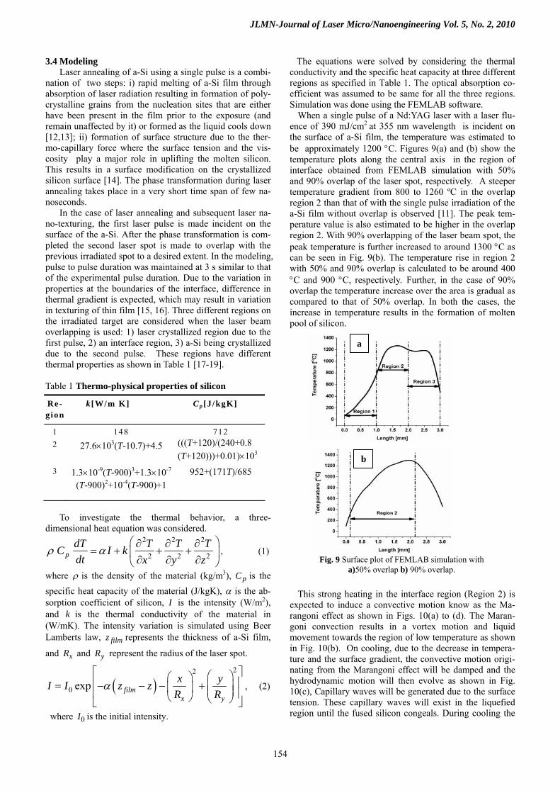
When a single pulse of a Nd:YAG laser with a laser flu-ence of 390 mJ/cm2 at 355 nm wavelength is incident on the surface of a-Si film, the temperature was estimated to be approximately 1200 °C. Figures 9(a) and (b) show the temperature plots along the central axis in the region of interface obtained from FEMLAB simulation with 50% and 90% overlap of the laser spot, respectively. A steeper temperature gradient from 800 to 1260 ºC in the overlap region 2 than that of with the single pulse irradiation of the a-Si film without overlap is observed [11]. The peak tem-perature value is also estimated to be higher in the overlap region 2. With 90% overlapping of the laser beam spot, the peak temperature is further increased to around 1300 °C as can be seen in Fig. 9(b). The temperature rise in region 2 with 50% and 90% overlap is calculated to be around 400 °C and 900 °C, respectively. Further, in the case of 90% overlap the temperature increase over the area is gradual as compared to that of 50% overlap. In both the cases, the increase in temperature results in the formation of molten pool of silicon.
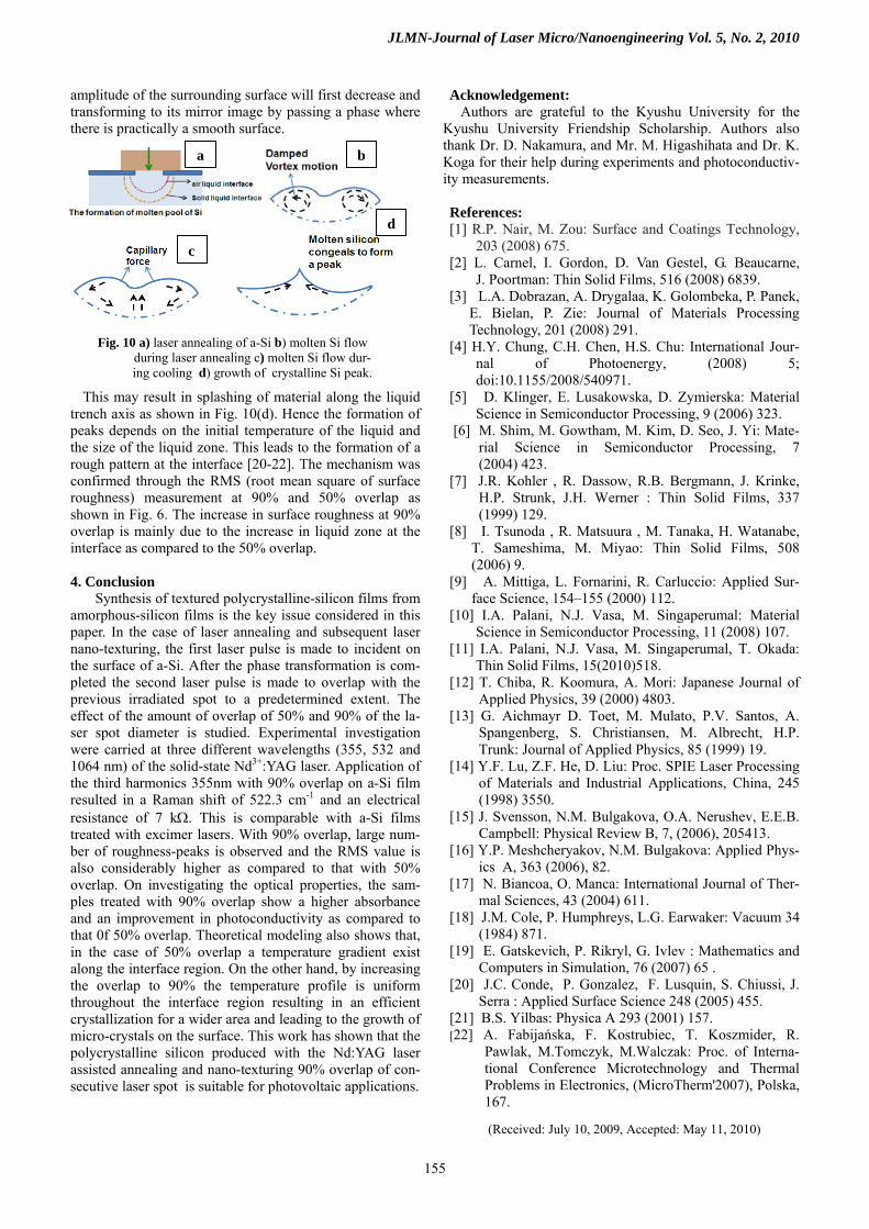
This strong heating in the interface region (Region 2) is
expected to induce a convective motion know as the Ma-rangoni effect as shown in Figs. 10(a) to (d). The Maran-goni convection results in a vortex motion and liquid movement towards the region of low temperature as shown in Fig. 10(b). On cooling, due to the decrease in tempera-ture and the surface gradient, the convective motion origi-nating from the Marangoni effect will be damped and the hydrodynamic motion will then evolve as shown in Fig. 10(c), Capillary waves will be generated due to the surface tension. These capillary waves will exist in the liquefied region until the fused silicon congeals. During cooling the
Re-gion
k [W/m K] C p [J /kgK]
1 148 712 2 27.6×10³(T-10.7)+4.5 (((T+120)/(240+0.8
(T+120)))+0.01)×103
3 1.3×10⁻⁹(T-900)3+1.3×10⁻⁷
(T-900)2+10-4(T-900)+1 952+(171T)/685
Fig. 9 Surface plot of FEMLAB simulation with a)50% overlap b) 90% overlap.
a
b
JLMN-Journal of Laser Micro/Nanoengineering Vol. 5, No. 2, 2010
155
amplitude of the surrounding surface will first decrease and transforming to its mirror image by passing a phase where there is practically a smooth surface.
This may result in splashing of material along the liquid
trench axis as shown in Fig. 10(d). Hence the formation of peaks depends on the initial temperature of the liquid and the size of the liquid zone. This leads to the formation of a rough pattern at the interface [20-22]. The mechanism was confirmed through the RMS (root mean square of surface roughness) measurement at 90% and 50% overlap as shown in Fig. 6. The increase in surface roughness at 90% overlap is mainly due to the increase in liquid zone at the interface as compared to the 50% overlap. 4. Conclusion Synthesis of textured polycrystalline-silicon films from amorphous-silicon films is the key issue considered in this paper. In the case of laser annealing and subsequent laser nano-texturing, the first laser pulse is made to incident on the surface of a-Si. After the phase transformation is com-pleted the second laser pulse is made to overlap with the previous irradiated spot to a predetermined extent. The effect of the amount of overlap of 50% and 90% of the la-ser spot diameter is studied. Experimental investigation were carried at three different wavelengths (355, 532 and 1064 nm) of the solid-state Nd3+:YAG laser. Application of the third harmonics 355nm with 90% overlap on a-Si film resulted in a Raman shift of 522.3 cm-1 and an electrical resistance of 7 kΩ. This is comparable with a-Si films treated with excimer lasers. With 90% overlap, large num-ber of roughness-peaks is observed and the RMS value is also considerably higher as compared to that with 50% overlap. On investigating the optical properties, the sam-ples treated with 90% overlap show a higher absorbance and an improvement in photoconductivity as compared to that 0f 50% overlap. Theoretical modeling also shows that, in the case of 50% overlap a temperature gradient exist along the interface region. On the other hand, by increasing the overlap to 90% the temperature profile is uniform throughout the interface region resulting in an efficient crystallization for a wider area and leading to the growth of micro-crystals on the surface. This work has shown that the polycrystalline silicon produced with the Nd:YAG laser assisted annealing and nano-texturing 90% overlap of con-secutive laser spot is suitable for photovoltaic applications.
Acknowledgement: Authors are grateful to the Kyushu University for the
Kyushu University Friendship Scholarship. Authors also thank Dr. D. Nakamura, and Mr. M. Higashihata and Dr. K. Koga for their help during experiments and photoconductiv-ity measurements.
References: [1] R.P. Nair, M. Zou: Surface and Coatings Technology,
203 (2008) 675. [2] L. Carnel, I. Gordon, D. Van Gestel, G. Beaucarne,
J. Poortman: Thin Solid Films, 516 (2008) 6839. [3] L.A. Dobrazan, A. Drygalaa, K. Golombeka, P. Panek,
E. Bielan, P. Zie: Journal of Materials Processing Technology, 201 (2008) 291.
[4] H.Y. Chung, C.H. Chen, H.S. Chu: International Jour-nal of Photoenergy, (2008) 5; doi:10.1155/2008/540971.
[5] D. Klinger, E. Lusakowska, D. Zymierska: Material Science in Semiconductor Processing, 9 (2006) 323.
[6] M. Shim, M. Gowtham, M. Kim, D. Seo, J. Yi: Mate-rial Science in Semiconductor Processing, 7 (2004) 423.
[7] J.R. Kohler , R. Dassow, R.B. Bergmann, J. Krinke, H.P. Strunk, J.H. Werner : Thin Solid Films, 337 (1999) 129.
[8] I. Tsunoda , R. Matsuura , M. Tanaka, H. Watanabe, T. Sameshima, M. Miyao: Thin Solid Films, 508 (2006) 9.
[9] A. Mittiga, L. Fornarini, R. Carluccio: Applied Sur-face Science, 154–155 (2000) 112.
[10] I.A. Palani, N.J. Vasa, M. Singaperumal: Material Science in Semiconductor Processing, 11 (2008) 107.
[11] I.A. Palani, N.J. Vasa, M. Singaperumal, T. Okada: Thin Solid Films, 15(2010)518.
[12] T. Chiba, R. Koomura, A. Mori: Japanese Journal of Applied Physics, 39 (2000) 4803.
[13] G. Aichmayr D. Toet, M. Mulato, P.V. Santos, A. Spangenberg, S. Christiansen, M. Albrecht, H.P. Trunk: Journal of Applied Physics, 85 (1999) 19.
[14] Y.F. Lu, Z.F. He, D. Liu: Proc. SPIE Laser Processing of Materials and Industrial Applications, China, 245 (1998) 3550.
[15] J. Svensson, N.M. Bulgakova, O.A. Nerushev, E.E.B. Campbell: Physical Review B, 7, (2006), 205413.
[16] Y.P. Meshcheryakov, N.M. Bulgakova: Applied Phys-ics A, 363 (2006), 82.
[17] N. Biancoa, O. Manca: International Journal of Ther-mal Sciences, 43 (2004) 611.
[18] J.M. Cole, P. Humphreys, L.G. Earwaker: Vacuum 34 (1984) 871.
[19] E. Gatskevich, P. Rikryl, G. Ivlev : Mathematics and Computers in Simulation, 76 (2007) 65 .
[20] J.C. Conde, P. Gonzalez, F. Lusquin, S. Chiussi, J. Serra : Applied Surface Science 248 (2005) 455.
[21] B.S. Yilbas: Physica A 293 (2001) 157. [22] A. Fabijańska, F. Kostrubiec, T. Koszmider, R.
Pawlak, M.Tomczyk, M.Walczak: Proc. of Interna-tional Conference Microtechnology and Thermal Problems in Electronics, (MicroTherm'2007), Polska, 167.
Fig. 10 a) laser annealing of a-Si b) molten Si flow during laser annealing c) molten Si flow dur-ing cooling d) growth of crystalline Si peak.
Laser a b
c
d
(Received: July 10, 2009, Accepted: May 11, 2010)