
Arnaud Rouzee- Alignement uni et tridimensionnel de molecules par impulsion laser femtoseconde

THÈSE NO 3080 (2004)
ÉCOLE POLYTECHNIQUE FÉDÉRALE DE LAUSANNE
PRÉSENTÉE À LA FACULTÉ SCIENCES DE BASE
Institut de physique des nanostructures
SECTION DE PHYSIQUE
POUR L'OBTENTION DU GRADE DE DOCTEUR ÈS SCIENCES
PAR
Ingénieur des arts et manufactures, École Centrale Paris, FranceDipl.-Ing. TU Wien, Autricheet de nationalité française
acceptée sur proposition du jury:
Dr J. Barth, directeur de thèseProf. M. Grätzel, rapporteur
Prof. J.I. Pascual, rapporteurProf. L. Porte, rapporteur
Lausanne, EPFL2004
INVESTIGATION OF LOW-DIMENSIONAL SUPRAMOLECULARARCHITECTURES BY LOW-TEMPERATURE SCANNING
TUNNELING MICROSCOPY
Sylvain CLAIR

Abstract
In this thesis we report investigations on supramolecular architectures assembled at well-
defined metal surfaces. Supramolecular chemistry is dedicated to the study and use of non-
covalent interactions to build highly organized molecular arrangements, aiming ultimately
at creating systems with tailored properties and useful functions. The adaptation of its
powerful principles to fabricate molecular systems at surfaces has already been proven to
be very promising; the extended possibilities for the choice of on the one hand molecules
with defined size, shape, symmetry and function, and on the other hand substrates with
controlled composition, symmetry and patterning allow for a quasi-infinite tuning of the
structure and properties of the respective assemblies.
The Scanning Tunneling Microscope (STM) is a tool particularly efficient for the
nanoscale elucidation of supramolecular systems at surfaces, simultaneously providing
topographic and spectroscopic information at the single-atom level. In this regard, a
new Low-Temperature STM (LT-STM) operational at temperatures in the range 5 to
400 K has been constructed. A detailed description of the instrument is provided and the
demonstration of its exquisite performance represents a major achievement. In addition
to local STM studies, complementary experiments were performed with a synchrotron
radiation source using integral techniques, namely X-ray Absorption Spectroscopy (XAS)
and X-ray Magnetic Circular Dichroism (XMCD).
We present results obtained with the linear organic linker 1,4-benzenedicarboxylic
acid (terephthalic acid - TPA) on the Au(111), Cu(111) and Cu(100) surfaces. The three-
dimensional design principles of supramolecular chemistry could be successfully adapted
to these low-dimensional systems.
TPA molecules adsorbed on Au(111) organize in two-dimensional molecular sheets,
wherein the typical one-dimensional hydrogen-bonded chain motif is found. We show that
the inhomogeneities induced by the surface reconstruction can be used to examine the
i
ii
response of the supramolecular self-assembly. In particular, variations in the hydrogen
bond length of up to 20% are encountered. On Cu(111), a strict commensurability of
the supramolecular sheet to the substrate is not possible because of the reduced lattice
spacing of the latter, and the creation of defects is analyzed.
Due to their peculiar reactivity, the elbow sites of the reconstructed Au(111) surface
act as nucleation centers in the epitaxial growth of transition metals (Fe, Co, Ni), leading
to the formation of regular arrays of nanoscale metallic islands. We take advantage of
this patterning to steer the formation of metallosupramolecular nano-architectures. Co-
deposited TPA molecules attack both Fe and Co clusters and metal-carboxylate linkages
evolve. Depending on the deposition parameters, nanoporous grids, mesoscopically orga-
nized stripes or truly one-dimensional linkages are obtained. Furthermore, the dynamics
of the formation of the nanogrids are monitored in situ.
Finally, we report investigations of the magnetic and electronic properties of surface-
supported coordination architectures by means of XAS and XMCD. We studied Fe-
terephthalate systems engineered on a Cu(100) substrate. Both mononuclear Fe(TPA)4
compounds and diiron centers structures in 2D Fe-TPA lattices exhibit a paramagnetic
behavior. Moreover, we demonstrate the decisive influence of the ligand rather than the
substrate on the electronic ground state of the metal centers, thus illustrating new vistas
to effectively tailor the valence state and magnetic moment of transition metal atoms at
surfaces.
0An electronic version of this thesis is available at http://library.epfl.ch/theses/
Version abregee
Dans ce rapport de these nous presentons les resultats obtenus avec des architectures
supramoleculaires assemblees sur des surfaces de monocristaux de metaux nobles. La
chimie supramoleculaire est dediee a l’etude et a l’utilisation d’interactions non covalentes
pour la fabrication de systemes hautement organises, avec pour but ultime la creation
d’assemblages fonctionalises aux proprietes controlees. L’adaptation de ses principes pro-
ductifs a des molecules sur des surfaces s’est deja averee etre tres prometteuse; l’etendue
des possibilites pour le choix d’une part de molecules de taille, forme, symetrie et fonction-
alite bien definies, et d’autre part d’un substrat possedant une composition, une symetrie
et une texturation donnees, permet de diriger la structure et les proprietes de tels ensem-
bles.
Le microscope electronique a effet tunnel (STM) est un outil particulierement bien
adapte pour l’etude nanometrique de systemes supramoleculaires sur des surfaces, puisqu’il
procure a la fois des informations topographiques et spectroscopiques au niveau de l’atome
unique. Nous avons donc entrepris la construction d’un nouveau microscope operationnel
dans la gamme de temperature 5 a 400 K (LT-STM). La description detaillee de l’instru-
ment est fournie, et la demonstration de ses hautes performances represente un resultat
important pour cette these. Parallelement aux etudes a l’echelle moleculaire par STM,
nous avons effectue des mesures complementaires avec deux techniques utilisant une source
de rayonnement synchrotron, la spectroscopie d’absorption des rayons X (XAS) et le
dichroısme circulaire magnetique des rayons X (XMCD).
Les resultats presentes ont ete obtenus avec la molecule d’acide benzene-1,4-dicarbo-
xylique (acide terephtalique - TPA) sur les surfaces Au(111), Cu(111) et Cu(100). Les
principes d’assemblage tridimensionnel de la chimie supramoleculaire ont pu etre adaptes
avec succes a ces systemes de basse dimensionnalite.
Les molecules de TPA adsorbees sur Au(111) s’organisent en couches bidimension-
iii
iv
nelles dans lesquelles on retrouve le motif typique de liaison par chaıne unidimensionnelle.
Nous montrons que les inhomogeneites dues a la reconstruction de surface peuvent etre
utilisees pour etudier la reponse de l’auto-assemblage supramoleculaire. En particulier,
nous trouvons des variations de la longueur des liaisons hydrogene jusqu’a 20%. Sur la
surface Cu(111), qui possede un parametre de maille reduit par rapport a Au(111), la
stricte commensurabilite de la couche supramoleculaire avec le substrat n’est pas realisee,
et la formation de defauts est analysee.
Du a leur reactivite particuliere, les coins de la reconstruction de la surface Au(111)
agissent comme centres de nucleation pour la croissance epitaxiale de metaux de transi-
tion, ce qui mene pour de faibles taux de couverture a la formation de reseaux reguliers
d’ılots metalliques nanometriques. Nous utilisons cette structuration de surface pour
diriger la fabrication de nano-architectures metallosupramoleculaires. Les molecules de
TPA codeposees attaquent les agregats de Fe et de Co pour former des liaisons metal-
carboxylate. En fonction des parametres de depot nous controlons la fabrication de grilles
nano-poreuses, de bandes mesoscopiques ordonnees, ou de lignes strictement unidimen-
sionnelles. De plus, la dynamique de formation des nano-grilles est suivie in situ.
Dans une derniere partie nous presentons les premieres characterisations des proprietes
magnetiques et electroniques d’architectures metallo-organiques sur des surfaces par XAS
et XMCD. Nous avons etudie des systemes Fe-terephtalate realises sur un substrat de
Cu(100). Les composes mononucleaires Fe(TPA)4 ainsi que les structures en reseau 2D a
deux centres de Fe sont paramagnetiques. De plus, nous demontrons l’influence decisive
du ligand, par comparaison au substrat, sur l’etat electronique fondamental des centres
metalliques. Ce resultat ouvre la voie a une grande variete de possibilites pour controler
efficacement l’etat de valence et le moment magnetique d’atomes de metaux de transition
sur des surfaces.
0Une version electronique de cette these est disponible a l’adresse http://library.epfl.ch/theses/
Table of Contents
Abstract i
Version abregee iii
Introduction 1
1 Scanning Tunneling Microscopy 7
1.1 Principles . . . . . . . . . . . . . . . . . . . . . . . . . . . . . . . . . . . . 7
1.2 Theoretical description . . . . . . . . . . . . . . . . . . . . . . . . . . . . . 10
1.2.1 Bardeen approach . . . . . . . . . . . . . . . . . . . . . . . . . . . . 10
1.2.2 Tersoff-Hamann formalism . . . . . . . . . . . . . . . . . . . . . . . 11
1.2.3 Tunneling spectroscopy . . . . . . . . . . . . . . . . . . . . . . . . . 12
1.3 Imaging adsorbed molecular species . . . . . . . . . . . . . . . . . . . . . . 15
2 Construction of a Low-Temperature Scanning Tunneling Microscope 19
2.1 General considerations - requirements . . . . . . . . . . . . . . . . . . . . . 19
2.2 The vacuum chamber . . . . . . . . . . . . . . . . . . . . . . . . . . . . . . 21
2.2.1 Vacuum generation . . . . . . . . . . . . . . . . . . . . . . . . . . . 21
2.2.2 The preparation chamber . . . . . . . . . . . . . . . . . . . . . . . 23
2.3 The cryostat . . . . . . . . . . . . . . . . . . . . . . . . . . . . . . . . . . . 27
2.4 The STM . . . . . . . . . . . . . . . . . . . . . . . . . . . . . . . . . . . . 31
2.4.1 Description . . . . . . . . . . . . . . . . . . . . . . . . . . . . . . . 31
2.4.2 Wiring . . . . . . . . . . . . . . . . . . . . . . . . . . . . . . . . . . 35
2.4.3 Mechanical stability . . . . . . . . . . . . . . . . . . . . . . . . . . 36
2.4.4 The STM-control electronics - recording modes . . . . . . . . . . . 38
2.5 STM test measurements . . . . . . . . . . . . . . . . . . . . . . . . . . . . 39
v
vi
3 Self-Assembly of Terephthalic Acid with Epitaxial Stress: Response of
the Hydrogen Bond 43
3.1 TPA on Au(111) . . . . . . . . . . . . . . . . . . . . . . . . . . . . . . . . 44
3.1.1 Description of the self-assembly . . . . . . . . . . . . . . . . . . . . 45
3.1.2 The Au(111) surface reconstruction . . . . . . . . . . . . . . . . . . 49
3.1.3 The 2D gas phase . . . . . . . . . . . . . . . . . . . . . . . . . . . . 57
3.2 TPA on Cu(111) . . . . . . . . . . . . . . . . . . . . . . . . . . . . . . . . 60
3.2.1 Description of the self-assembly . . . . . . . . . . . . . . . . . . . . 60
3.2.2 Dislocations in the molecular layer . . . . . . . . . . . . . . . . . . 63
4 Metallosupramolecular Nanoarchitectures 67
4.1 Mesoscopic patterning of the Au(111) surface by deposition of metallic
impurities . . . . . . . . . . . . . . . . . . . . . . . . . . . . . . . . . . . . 69
4.2 Exploiting the Fe,Co/Au(111) template to monitor coordination reactions . 71
4.3 Metal-organic nano-texturing . . . . . . . . . . . . . . . . . . . . . . . . . 79
5 Electronic and Magnetic State of Metal Centers in Surface-Supported
Coordination Architectures 85
5.1 XAS and XMCD Spectroscopy . . . . . . . . . . . . . . . . . . . . . . . . . 87
5.2 XAS/XMCD of Fe-TPA coordination compounds . . . . . . . . . . . . . . 92
5.2.1 Description of the structures . . . . . . . . . . . . . . . . . . . . . . 93
5.2.2 XAS investigations . . . . . . . . . . . . . . . . . . . . . . . . . . . 95
5.2.3 XMCD investigations . . . . . . . . . . . . . . . . . . . . . . . . . . 96
Conclusions and Future Directions 103
Acknowledgements 107
Bibliography 109
Curriculum Vitae 123
Introduction
The properties of condensed matter on the atomic scale are quite different from those ob-
served in everyday life. This has been known since the development of quantum mechan-
ics at the beginning of the 20th century. In the last two decades however, technological
progress has made it possible to substantially advance control of matter at the nanometer
level. Scientists are now able to arrange atoms and molecules into (nano)structures of de-
signed shape, size, and chemical composition. Equally important, the physical properties
of such structures can be studied with unprecedented sensitivity, structural and chemical
detail. The entire term nanoscience (and nanotechnology) designates investigations and
use of objects with dimensions smaller than 100 nm and made out of a few (up to 106)
atoms or molecules. With regard to the nature of the systems involved and the techniques
used, nanotechnology is positioned at the cross-road between physics, material science,
chemistry and biology, and is therefore accumulating experience from the synergetic ex-
pertise of these disciplines (see, e.g, [1,2]). In particular, supramolecular chemistry with
its profusion of molecule-based compounds and processes constitute an appealing method
for engineering novel functional nanosystems [3].
The whole field of surface and nanoscale science is able to provide precise and extensive
analysis on the structural, chemical and electronic state of supramolecular architectures at
well-defined surfaces. However, among the various tools available, Scanning Tunneling Mi-
croscopy (STM) provides a unique and detailed knowledge in real space of low-dimensional
systems, in addition to spectroscopic information on a local scale. Moreover, a legion of
recent studies attest to its value for the elucidation of fundamental phenomena in sur-
face chemistry in exquisite detail: topology of supramolecular assemblies and molecular
conformations [4–11], chiral specificity [5,12–14], pathways of chemical reactions [15–20],
and catalytic functionality [21,22]. Notably, when supported by computational modeling,
and employed in combination with powerful integral methods like X-ray absorption or
1
2 INTRODUCTION
X-ray photoemission spectroscopy, an advanced understanding of molecular nanosystems
can be gained.
In order to develop a rationale for molecular engineering in two dimensions, we need
a comprehensive characterization of the coupling schemes of adsorbed complex molecules
mediated by their functional groups, their bonding to the employed solid substrates, and
the organization principles resulting from the balance of these interactions. This un-
derstanding will pave the way towards novel bottom-up strategies for the fabrication of
supramolecular nanostructures potentially useful as novel materials in molecular electron-
ics, magneto-recording devices, nano-templating, chemical sensing schemes, host-guest
interactions or catalysis. A wide range of applications is envisioned, from nano-motors,
nano-devices or nano-reactors, to computational systems based on the quantum proper-
ties of individual molecules, optical components with fluorescent molecules, nano-porous
materials for gas storage or drug release, etc. In addition, there is a basic interest to study
local elementary processes in chemistry or complex biological systems.
Molecular self-assembly relies on interactions between complex molecules containing
specific functional groups. Self-assembly is abundant in nature, where the process is used
to successfully create complex functional biological structures. The molecular level design
of new materials by self-assembly expanded extensively in the past decades [23–26] under
the banner of the multidisciplinary fields of crystal engineering [27–29] and supramolecular
chemistry [3,30,31]. If molecules are built by connecting atoms with covalent bonds, super-
molecules are assembled on the next level of complexity by binding molecules together with
directional intermolecular interactions, non-covalent in nature. Supramolecular species are
characterized by the spatial arrangement of their components, their functionality, and the
nature of the intermolecular bonds that hold these components together. Various types of
interactions may be distinguished, which present different degrees of strength, direction-
ality, and dependence on distance and angles: metal-ligand coordination, electrostatic
forces, hydrogen bonding, van der Waals interactions, donor-acceptor interactions, etc.
Their strengths range from weak or moderate as in hydrogen bonds, to strong or very
strong for metal-ligand coordination. Intermolecular forces are generally weaker than co-
valent bonds, so that supramolecular species are thermodynamically less stable, kinetically
more labile and dynamically more flexible than molecules. Thus, supramolecular chem-
istry is concerned with soft bonds and represents a chemistry ”beyond the molecule” [3].
3
Among the various driving forces governing molecular self-assembly, hydrogen bond-
ing attracts particular interest. It is of pivotal importance in biological systems and
in organic host-guest molecular complexes: structural aspects of DNA and DNA bind-
ing agents, protein conformations and folding, or receptor functions are examples where
the natural chemistry of hydrogen bonding is extensively involved [31, 32]. Of all direc-
tional intermolecular interactions, hydrogen bonding is the most important and versatile
one. Three-dimensional structures may be readily and specifically assembled by hydro-
gen bonding, incorporating a large degree of flexibility due to weak intermolecular forces
holding the molecules. As the interaction is weaker than covalent bonding and in the
range of thermal energies at ambient conditions, it may be reversed - an intrinsic er-
ror correction mechanism is characteristic for hydrogen-bonded assemblies, which leads
ultimately to the most thermodynamically favorable structures. An important feature
encountered in hydrogen bonded architectures is cooperativity - being individually weak,
together H-bonds become stronger, which enables non-covalent synthesis, based on the
reversible formation of multiple hydrogen bonds to be accomplished. Hydrogen bonding
is responsible for the determination of molecular conformation, molecular aggregation and
functionality of a vast number of supramolecular systems [3,31,33,34]. At solid substrates,
particularly on single crystal metal surfaces, hydrogen bonding was successfully explored
to advance supramolecular engineering, where its directionality facilitates fabrication of
highly organized assemblies [6,35–41]. Due to the great flexibility of this weak interaction,
employing hydrogen bonding for the fabrication of surface-supported supramolecular ar-
chitectures allows deliberate design of complex topologies with possible control over the
final structures and functionalities [7].
Since the introduction of the coordination concept more than a century ago [42], the
use of transition metal centers and coordination chemistry for directing the formation of
complex structures has evolved into one of the most widely used strategies for organizing
molecular building blocks into supramolecular architectures [3,31,43,44]. The predictable
and directional bonding of organic ligands allows for the engineering of supramolecular
coordination complexes with extraordinary structures and properties: rotaxanes and cate-
nanes, synthetic receptors, molecular cages, as well as multicomponent assemblies such
as chains, nanoporous networks or helices are already classical examples of coordination-
driven self-assembly [31,45–50]. Solid state chemistry takes advantage of the coordination
4 INTRODUCTION
bonding approach, since rational crystal engineering of solid materials is crucially depen-
dent on predictability and rigidity - e.g., provided by organometallic compounds, where
C-moieties of organic molecules couple to a metal [51, 52]. Transition metal complexes
also play a tremendous role in catalysis. The mimics of enzymatic specificity in chemical
asymmetric synthesis is tentatively approached by use of transition-metal-based cata-
lysts [53], whereas supported metal-organic catalytic materials are expected to bridge the
gap between homogeneous and heterogeneous catalysis, bringing the concepts and tools
of chemistry to surface science [54,55]. Molecular magnetism constitutes another promis-
ing facet of modern coordination chemistry and in recent years the field has produced
magnificent solid-state structures with intriguing magnetic properties [56]. Coordination
bonds may be decisive in molecular recognition and offer an excellent means for the fabri-
cation of surface-supported complex molecular arrangements: however, their exploration
for surface supramolecular chemistry is yet in its infancy [57–59].
In this thesis we investigated molecular nanosystems at well-defined metal surfaces.
For this purpose, a Low-Temperature Scanning Tunneling Microscope (LT-STM) has
been constructed, which provides nanoscale insight into supramolecular architectures.
The samples were prepared in situ in Ultra High Vacuum (UHV) conditions in order to
obtain atomically clean surfaces where a precise amount of material was deposited. The
direct monitoring of the two-dimensional molecular organization allows for the elucidation
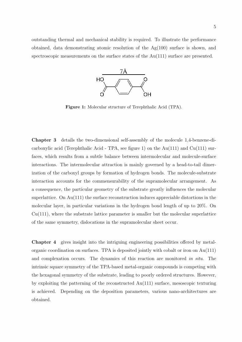
of some of the key principles governing self-assembly at surfaces. The molecule used
(figure 1) was chosen for its simple design and its ability to form hydrogen-bond-based
synthons and metal-ligand coordination.
The present report is organized as follows:
Chapter 1 is a brief introduction to the main technique used, i.e., Scanning Tunneling
Microscopy (STM). A theoretical approach based on the Bardeen approximation is de-
scribed, which gives the required qualitative understanding for the interpretation of STM
images and Scanning Tunneling Spectroscopy (STS). Additionally, the specific issue of
imaging adsorbed molecular species is raised.
Chapter 2 presents the new experimental setup, a Low-Temperature STM (LT-STM)
working in Ultra-High Vacuum (UHV). The design and the construction of this system
has been achieved within the framework of the present thesis. For the investigations an
5
outstanding thermal and mechanical stability is required. To illustrate the performance
obtained, data demonstrating atomic resolution of the Ag(100) surface is shown, and
spectroscopic measurements on the surface states of the Au(111) surface are presented.
Figure 1: Molecular structure of Terephthalic Acid (TPA).
Chapter 3 details the two-dimensional self-assembly of the molecule 1,4-benzene-di-
carboxylic acid (Terephthalic Acid - TPA, see figure 1) on the Au(111) and Cu(111) sur-
faces, which results from a subtle balance between intermolecular and molecule-surface
interactions. The intermolecular attraction is mainly governed by a head-to-tail dimer-
ization of the carboxyl groups by formation of hydrogen bonds. The molecule-substrate
interaction accounts for the commensurability of the supramolecular arrangement. As
a consequence, the particular geometry of the substrate greatly influences the molecular
superlattice. On Au(111) the surface reconstruction induces appreciable distortions in the
molecular layer, in particular variations in the hydrogen bond length of up to 20%. On
Cu(111), where the substrate lattice parameter is smaller but the molecular superlattice
of the same symmetry, dislocations in the supramolecular sheet occur.
Chapter 4 gives insight into the intriguing engineering possibilities offered by metal-
organic coordination on surfaces. TPA is deposited jointly with cobalt or iron on Au(111)
and complexation occurs. The dynamics of this reaction are monitored in situ. The
intrinsic square symmetry of the TPA-based metal-organic compounds is competing with
the hexagonal symmetry of the substrate, leading to poorly ordered structures. However,
by exploiting the patterning of the reconstructed Au(111) surface, mesoscopic texturing
is achieved. Depending on the deposition parameters, various nano-architectures are
obtained.

6 INTRODUCTION
In chapter 5 the electronic structure and the magnetic properties of metal centers
in surface-supported metal-organic networks are characterized for the first time. The
use of X-ray Absorption Spectroscopy (XAS) and X-ray Magnetic Circular Dichroism
(XMCD) allows unprecedented insight into the valence state and magnetic moment of
the transition-metal ions. The decisive influence of the ligand rather than the substrate
on their electronic ground state is demonstrated. The experiments presented were per-
formed in the European Synchrotron Radiation Facility (ESRF) in Grenoble on Fe+TPA
coordination compounds on the Cu(100) surface.
Chapter 1
Scanning Tunneling Microscopy
This chapter presents a basic introduction to Scanning Tunneling Microscopy (STM).
This technique owes its immense success to its direct atomic scale imaging and manip-
ulation capabilities coupled to the possibility of extracting information on the electronic
structure of surfaces on a local scale. A theoretical approach based on the Bardeen
approximation is described, which underlines the difficulty encountered when analyzing
STM images, and reveals the relevant physical quantities governing Scanning Tunneling
Spectroscopy (STS). In the following section the specific problem of adsorbate imaging is
raised. For an overview of the STM capabilities see, e.g., Ref. [19, 60–64].
1.1 Principles
Scanning tunneling microscopy, invented by Binnig and Rohrer in 1982 [65], is a technique
strongly related to classical electron tunneling experiments pioneered in the early sixties
by Giaever and coworkers [66]. In both cases the quantity of interest is the electronic
current I tunneling between two electrodes biased at a voltage V . The electrodes are sep-
arated by a thin insulating medium. The amount of current flowing for a given potential
difference V depends on the density of electronic states (DOS) in the electrodes, and thus
contains valuable information about the electronic structure of the surfaces of the elec-
trodes. In classical planar tunnel junctions an oxide is mostly used as insulator, whereas a
vacuum gap serves as tunnel barrier in STM. The gap can also consist of gaseous or liquid
substances, e.g., air or electrolyte. In STM one electrode is tip shaped, i.e., microscopic,
and can be positioned in three dimensions relative to the second electrode, contrary to
7
8 CHAPTER 1. SCANNING TUNNELING MICROSCOPY
classical tunnel experiments where two static planar electrodes are used. Thus STM offers
the advantage of performing spatially resolved tunneling experiments.
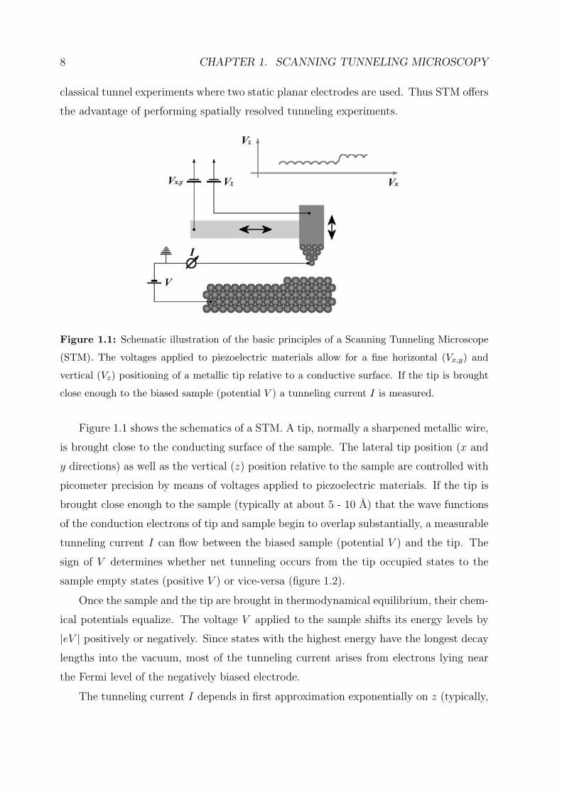
Figure 1.1: Schematic illustration of the basic principles of a Scanning Tunneling Microscope
(STM). The voltages applied to piezoelectric materials allow for a fine horizontal (Vx,y) and
vertical (Vz) positioning of a metallic tip relative to a conductive surface. If the tip is brought
close enough to the biased sample (potential V ) a tunneling current I is measured.
Figure 1.1 shows the schematics of a STM. A tip, normally a sharpened metallic wire,
is brought close to the conducting surface of the sample. The lateral tip position (x and
y directions) as well as the vertical (z) position relative to the sample are controlled with
picometer precision by means of voltages applied to piezoelectric materials. If the tip is
brought close enough to the sample (typically at about 5 - 10 A) that the wave functions
of the conduction electrons of tip and sample begin to overlap substantially, a measurable
tunneling current I can flow between the biased sample (potential V ) and the tip. The
sign of V determines whether net tunneling occurs from the tip occupied states to the
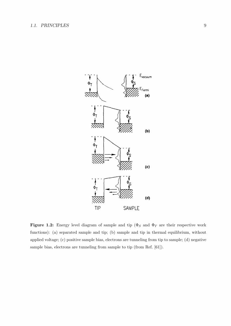
sample empty states (positive V ) or vice-versa (figure 1.2).
Once the sample and the tip are brought in thermodynamical equilibrium, their chem-
ical potentials equalize. The voltage V applied to the sample shifts its energy levels by
|eV | positively or negatively. Since states with the highest energy have the longest decay
lengths into the vacuum, most of the tunneling current arises from electrons lying near
the Fermi level of the negatively biased electrode.
The tunneling current I depends in first approximation exponentially on z (typically,
1.1. PRINCIPLES 9
Figure 1.2: Energy level diagram of sample and tip (ΦS and ΦT are their respective work
functions): (a) separated sample and tip; (b) sample and tip in thermal equilibrium, without
applied voltage; (c) positive sample bias, electrons are tunneling from tip to sample; (d) negative
sample bias, electrons are tunneling from sample to tip (from Ref. [61]).
10 CHAPTER 1. SCANNING TUNNELING MICROSCOPY
a 1 A displacement in z implies a ten-fold variation in I). The individual atoms or
adsorbates of the sample surface give rise to substantial current variations as the tip is
scanned in x and y. In the constant-current mode of operation the current I, which is
typically in the range 0.1 – 5 nA for metal surfaces, is compared with a preset value I0 in
a feedback loop. The difference between I and I0 is converted into a correction voltage
and sent to the z transducer.
In this way the tunneling current is kept constant by approaching or withdrawing
the tip from the sample. Recording the feedback signal as a function of the lateral tip
position yields a three-dimensional (3D) map of the surface topography. More precisely
z(x, y)|I,V represents a surface of constant local density of electron states (LDOS) of the
sample at a given energy (in fact the integral of the LDOS from Fermi level to the energy
considered is measured). This makes the interpretation of the data sometimes delicate,
especially for non-metallic systems. A proper modeling of the tunneling process in a STM
would require the knowledge of the 3D electron potential in the gap region between the
tip and the sample, the description of the electronic states of both the sample and the
tip, and the description of the spatial extension of the electron wave functions in the
tunnel gap. The poor symmetry of the system, the unknown geometry of the tip, and
tip-sample interactions make this task extremely difficult. Series of approximations are
usually imposed to model the real system.
1.2 Theoretical description
1.2.1 Bardeen approach
In 1961 Bardeen proposed a formalism [67] for describing the planar geometry of the
classical tunneling experiments, the so-called Hamiltonian approximation. By neglecting
the interaction between the two separately described electrodes the tunneling current for
weak wave function overlap is
I(V ) =2πe
∑µ,ν
|Mµ,ν |2 δ(Eµ − eV − Eν) ×(f(Eµ − eV, T ) [1 − f(Eν , T )] − f(Eν , T ) [1 − f(Eµ − eV, T )]
)(1.1)
1.2. THEORETICAL DESCRIPTION 11
where the summation goes over all quantum eigenstates µ and ν of the independent
electrodes; the eigenvalues Eµ and Eν are given with respect to the (common) Fermi level;
V is the applied voltage between the electrodes, f(E, T ) is the Fermi-Dirac distribution
function and T is the temperature. The δ-function indicates that the tunneling electron
transfer from one electrode to the other is an elastic process, whereas the Fermi-Dirac
functions take into account that tunneling occurs from filled to unfilled states. In the
limits of small voltage and temperature, Eq. (1.1) becomes
I =2π
e2V
∑µ,ν
|Mµ,ν |2 δ(Eµ − EF ) δ(Eν − EF ) (1.2)
The matrix element Mµ,ν represents the overlap in the gap region of the electrode
wave functions and is given by the current density operator through a surface S lying
entirely within the gap region:
Mµ,ν = − 2
2m
∫S
dS (Ψ∗µ∇Ψν − Ψµ∇Ψ∗
ν) (1.3)
1.2.2 Tersoff-Hamann formalism
The planar geometry presented above is not well suited for describing a STM experiment
where one of the electrodes is a tip. Tersoff and Hamann [68] proposed specific and more
realistic wave functions for calculating the matrix element Mµ,ν .
The surface wave function Ψν is described by a set of periodic surface plane wave
functions decreasing exponentially in the normal direction (z):
Ψν = Ψ k‖,E(r) =∑
G
a G exp
[−
√k2 + (k‖ + G)2 .z
]× exp
[i(k‖ + G).r‖
](1.4)
where k =√
2mφ2 is the inverse decay length for the wave functions in vacuum, φ is the
work function, k‖ is the surface wave vector of the state, and G is a surface reciprocal-
lattice vector.
The tip is modeled as locally spherical with radius of curvature R. Its wave function
is restricted to the asymptotic spherical form (s-wave)
Ψµ = Aµe−k|r−r0|
|r − r0| (1.5)
where Aµ is a normalization constant, r0 is the position of the center of curvature of the
tip and k is defined as above.
12 CHAPTER 1. SCANNING TUNNELING MICROSCOPY
The matrix element (1.3) becomes then simply
Mµ,ν = −2π2
mAµΨν(r0) (1.6)
and the tunneling current (1.2) can be written as
I =e2V
× (2π)3
4
m2
∑µ
|Aµ|2 δ(Eµ − EF )∑
ν
|Ψν(r0)|2δ(Eν − EF ) (1.7)
The relevant physical quantities here are
ρt(EF ) =∑
µ
|Aµ|2 δ(Eµ − EF ) (1.8)
the density of states of the tip at the Fermi level, and
ρs(r0, EF ) =∑
ν
|Ψν(r0)|2δ(Eν − EF ) (1.9)
the local density of states (LDOS) of the (unperturbed) surface at the Fermi level mea-
sured at the center of curvature of the tip.
Consequently the tunneling current is:
I =e2V
βρs(r0, EF ) ρt(EF ) (1.10)
where β is a constant.
This model is only valid in the limit of low temperature and bias voltage and for a
weak coupling between the electrodes, but shows that in first approximation constant-
current STM topographs can be simply interpreted as contours of constant ρs(EF ), the
LDOS of the surface at the Fermi level.
1.2.3 Tunneling spectroscopy
The expression (1.10) derived by Tersoff and Hamman can be extended for higher voltage
levels (but in the limits of V small in comparison with the electrode work function) [69,70]:
I =e2V
β
∫ EF +eV
EF
dE ρs(r‖, E) T (E, V, z) ρt(E − eV ) (1.11)
with the transmission coefficient T (E, V, z) corresponding to a correcting factor accounting
for the voltage drop in the vacuum region disregarding its k‖ dependence. The sample
1.2. THEORETICAL DESCRIPTION 13
LDOS ρs(r‖, E) is taken in the surface plane right under the tip. The vertical dependence
T (E, V, z) is evaluated as
T (E, V, z) = exp(−2z
√2mΦ
2) (1.12)
with the mean barrier height being
Φ =Φt + Φs
2+
eV
2− E (1.13)
Equation (1.11) shows that all electronic states of energy between EF and EF + eV are
contributing to the tunneling current with varying weight. It is however possible in first
approximation to extract the surface LDOS from I(V ).
By taking the derivative of the tunneling current (1.11) with respect to the voltage,
one obtains:
dI
dV∝ ρs(r‖, EF + eV ) T (EF + eV, V, z) ρt(EF )
+∫ EF +eV
EFdE ρs(r‖, E) dT (E,V,z)
dVρt(E − eV )
−e∫ EF +eV
EFdE ρs(r‖, E) T (E, V, z) dρt(E−eV )
dV(1.14)
For a tip of ”flat” density of states (ρt(E)=const.) we find
dI
dV∝ ρs(r‖, EF + eV ) T (EF + eV, V, z) ρt(EF )
+∫ EF +eV
EFdE ρs(r‖, E) dT (E,V,z)
dVρt(E − eV ) (1.15)
The second term in equation (1.15) is negligible for small tunnel voltages or induces only
small shifts in the position of the surface electronic states [69, 71], so we can write as a
good approximation:
dI
dV∝ ρs(r‖, EF + eV ) T (EF + eV, V, z) (1.16)
The differential tunneling conductance is proportional to the local density of states for a
transmission coefficient varying slowly with V .
14 CHAPTER 1. SCANNING TUNNELING MICROSCOPY
Thermal broadening
At finite temperature the electronic state occupancies are modulated by the Fermi-Dirac
function f(E, T ):
I ∝∫ +∞
−∞dE ρs(r‖, E) T (E, V, z) ρt(E − eV ) f(E − eV, Tt)[1 − f(E, Ts)] (1.17)
where the integral is now taken over an infinite energy range, and Ts and Tt are the tem-
peratures of the sample and of the tip, respectively. In fact this is equivalent to Eq. (1.11),
where in the limit of small temperature the Fermi-Dirac function is approximated as a
step function.
Following the approximations leading to Eq. (1.16), the differential tunneling conduc-
tance is nowdI
dV∝
∫ +∞
−∞dE
−df(E − eV, Tt)
dVρs(r‖, E) T (E, V, z) (1.18)
The function−df(E−eV,Tt)
dV is similar to a Gaussian function with a full width at half
maximum of about 3.5 kBT [72] (where kB is the Boltzmann constant).
This result shows that, within the Tersoff and Hamann approximations, a STS spec-
trum at finite temperature results from the convolution of the sample LDOS with a
Gaussian function. At room temperature the broadening amounts to 90 meV and can be
very limitative for studying particular electronic features. Note that in this formalism,
where we consider a tip DOS without any energy dependent feature, the temperature of
the tip is the relevant parameter. To increase substantially the spectroscopic resolution,
it is thus necessary to cool down the STM, and especially the tip, to low temperature.

1.3. IMAGING ADSORBED MOLECULAR SPECIES 15
1.3 Imaging adsorbed molecular species
The interplay of topography and electronic structure becomes crucial when interpreting
STM data obtained on molecular adsorbates. A well-known counterintuitive example is
atomic oxygen chemisorbed on a metal surface, which appears as a depression in STM
images even if the atom is positioned above the metal surface layer [15]. STM patterns of
molecules often show internal structure and details but the interpretation is not straight-
forward due to the fact that protrusions on the STM image do not necessarily represent
actual lateral position of atoms.
Before the first successful STM experiments with clearly resolved organic molecules
were reported [73–75] it appeared questionable whether insulating molecules can be im-
aged by STM at all. As stated above, the tunneling current is proportional to the sample
LDOS near the Fermi level EF within the framework of the transfer Hamiltonian theory
of STM. Most organic molecules have a large energy gap between the highest occupied
(HOMO) and the lowest unoccupied (LUMO) molecular orbitals. If physisorbed on a
metal surface, the molecule-related states are usually far away from the substrate Fermi
energy. The HOMO- and LUMO- derived resonances are typically several eV below and
above EF , respectively. Therefore, the molecules contribution to the LDOS near EF is
rather small and at first glance one might expect organic molecules to be transparent for
tunneling electrons at low bias voltage.
These considerations are of general importance for the imaging of molecules adsorbed
on metal surfaces. Non-resonant tunneling occurs and the contribution of the adsorbate to
the current comes from tails of molecular orbital resonances crossing the Fermi level. The
DOS associated with these tails are usually rather small at the Fermi level, which explains
why contributions from the substrate itself cannot be neglected, despite the appreciable
difference in geometric height.
To interpret STM images of molecules the electronic structure of the adsorbate-
substrate system can be calculated, whereby various levels of approximation are used
ranging from Huckel calculations to first-principles self-consistent methods based mainly
on the density functional theory (DFT). Again, the tunneling current is frequently re-
duced to the LDOS of the sample at the Fermi energy. In this approach the tip and the
surface are treated separately, which neglects any interaction between them and is valid
only in the limit of large tip-surface distances (similarly to the Tersoff-Hamann model,
16 CHAPTER 1. SCANNING TUNNELING MICROSCOPY
where the electrodes are treated separately and the result is derived for small voltages,
cf. section 1.2.2). Secondly, a severe approximation is made to the structure of the tip
apex and any tip dependence of the image is lost. This can be accounted for by regarding
p and d states as tip orbitals [76] or by describing the tip apex by a cluster of a small
number of atoms [77,78].
Another approach is the proper description of the interaction between sample and
tip with a scattering theory formalism. The influence of tip-sample interactions becomes
apparent in the imaging of adsorbed alkali metal atoms. Although they are known to
substantially increase the LDOS at EF , they are frequently transparent in STM data [79].
The basic idea of the scattering theory formalism is to consider the tunnel gap as a
two-dimensional defect inserted between two semi-infinite periodic systems. The tunnel-
ing event is then viewed as a scattering process. An example is the electron scattering
quantum chemical (ESQC) approach developed by Sautet and Joachim [80]. The tunnel
junction is modeled by the approach of substrate and tip semi-infinite bulk solids. The
adsorbate is chemisorbed on the substrate surface, while the tip apex, attached to the
second semi-infinite solid, is modeled by a cluster of 1-15 atoms. Coupling with the tip
and substrate electron reservoirs is hence fully taken into account.
Aromatic molecules represent an important group of adsorbates. Notably they can
bear functional groups that can be exploited for building diverse molecular nanostructures
at surfaces. Benzene was the first molecule of this class to be successfully imaged on a
surface by high resolution STM: coadsorbed with CO on Rh(111) [74], benzene molecules,
which are bound at threefold substrate hollow sites as determined by LEED [81], appear as
three lobes forming a triangle in STM topographs. The lobes are located near the center
of C-C bonds, in between underlying Rh substrate atoms as evidenced by ESQC [82]: the
molecule appears to have 3-fold symmetry because molecular orbitals are hybridized with
the rhodium substrate atoms below. As a consequence the STM image of benzene on a
close-packed transition metal surface does not show positions of molecular C atoms but
specific C-C bonds.
High-resolution STM studies, combined with calculations of LUMO and HOMO, were
performed with more complex aromatic species in the early 90’s. Particularly, a compar-
ative study of naphthalene (C10H8) and azulene (C10H8) adsorption on Pt(111) demon-
strates that a simple calculation methodology based on extended Huckel molecular orbital

1.3. IMAGING ADSORBED MOLECULAR SPECIES 17
theory adequately predicts details of internal structure [83]. Electron and hole density
plots show very good agreement with the actual STM data and enable the reliable iden-
tification of molecular species.
A detailed description of several theoretical approaches to the contrast mechanism of
adsorbate imaging with the scanning tunneling microscope is given in a review article by
Sautet [84].

Chapter 2
Construction of a Low-Temperature
Scanning Tunneling Microscope
The experimental setup that has been developed and built up in the framework of the
present thesis is shown in figure 2.1. The motivation for constructing a new setup was to
obtain a Scanning Tunneling Microscope (STM) working in Ultra High Vacuum (UHV) at
variable temperature (in the range 5 to 400 K) with outstanding thermal and mechanical
stability.
Since the discovery of STM by Binnig and Rohrer in 1982 [65] and the first develop-
ments of low temperature STM [85–87], several home-built low temperature microscopes
(LT-STM) were realized (see, e.g., [88–93]). The setup presented here is mostly inspired
from the work of Meyer [94], which has been commercialized [95] after the beginning of
this thesis.
2.1 General considerations - requirements
A Scanning Tunneling Microscope is a tool designed for observation and manipulation of
surfaces at the atomic scale. To achieve this goal, a supreme control of the conditions
and the environment of the sample studied at this scale is required. The tip is positioned
from 5 to 10 A above the sample surface with a precision lower than 0.01 A due to the
exponential I(z) characteristics, and laterally the position control must be a mere fraction
of the interatomic spacing, which is for crystal surfaces typically around 3 A.
The main challenge is to get rid of most of external noise. Mechanical noise comes
19
20 CHAPTER 2. CONSTRUCTION OF A LT-STM
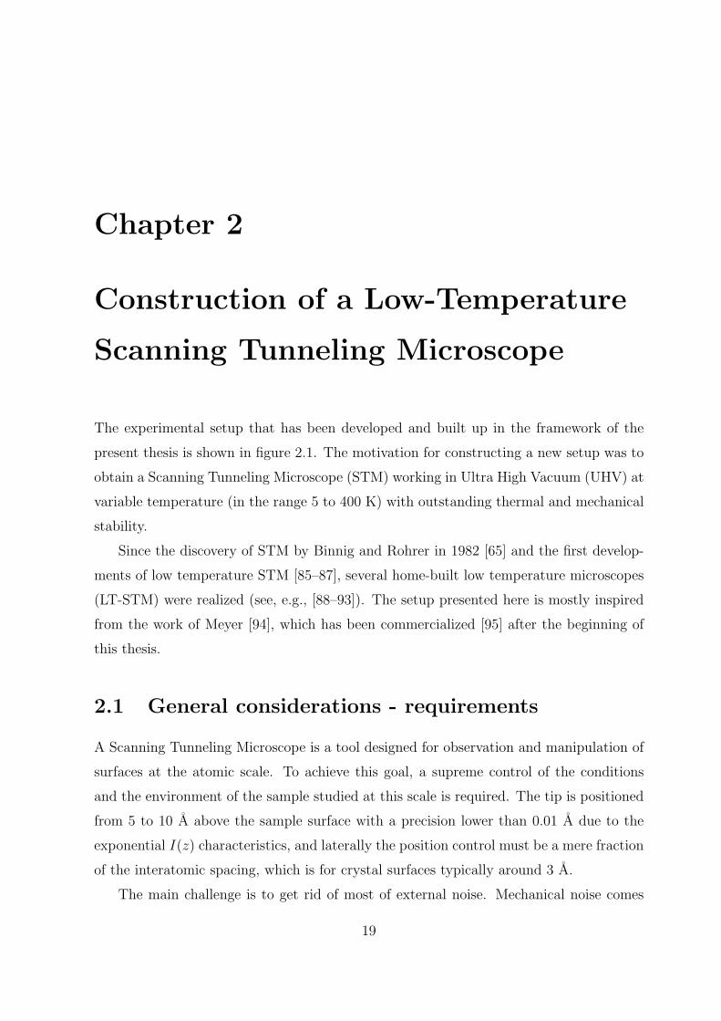
Figure 2.1: Global view of the experimental setup: (1) STM chamber, (2) Preparation chamber,
(3) He bath cryostat, (4) He flux cryostat (manipulator), (5) Suspension legs. Model made with
Solidworks [96].
from vibrations of the building as well as acoustic waves in the laboratory. Electrical noise
comes from all the electromagnetic perturbations generated by the power supply network
and other electronic instruments. Pneumatic suspension legs represent a good way to
insulate the system from mechanical disturbances (Fig. 2.1). The whole apparatus is held
on four suspension legs [97], and the entire bath cryostat sits on three more legs [98].
The STM itself is suspended by springs, and all the different parts were designed so as to
make the assembly as rigid as possible. The vibration eigenfrequencies are in this manner
shifted to high values and resonance phenomena are diminished.
Electromagnetical insulation is delicate. The wires transporting critical signals (tun-
neling current, z signal, sample bias) are carefully shielded (coaxial wires). In addition,
the tunneling current signal is amplified and filtered at the exit of the vacuum chamber.
Experimenting in a vacuum chamber is an accurate way to get good control of the
2.2. THE VACUUM CHAMBER 21
sample environment, even if STM studies are also possible in air or in a liquid. The
sample preparation is made in situ in such a way as to obtain an atomically clean and
crystallographically well-defined surface where a precise amount of material can be de-
posited. Many complementary analysis methods are available, using electron (LEED,
Auger Spectroscopy, . . . ) or photon (XPS, IR-spectroscopy, . . . ) beams.
Working at cryogenic temperature is very advantageous in terms of stability and res-
olution in comparison with room temperature where the surface mobility is high, thermal
drift is non negligible and where the electronic properties are broadened [99, 100]. Con-
trolled temperature allows furthermore qualitative and quantitative access to the various
temperature dependent phenomena that take place on a surface, like diffusion, chemical
reaction, or structural, electronic or magnetic transitions (superconductive state, charge
density waves, ferro/antiferromagnetic transition, etc. . . ).
Simultaneous achievement of on the one hand the mechanical decoupling required for
the stability and on the other hand the thermal coupling required to reach low tempera-
tures is in many ways impossible. Furthermore, the materials at disposal are restricted to
UHV-compatible ones. The solutions retained are the result of a series of compromises.
2.2 The vacuum chamber
2.2.1 Vacuum generation
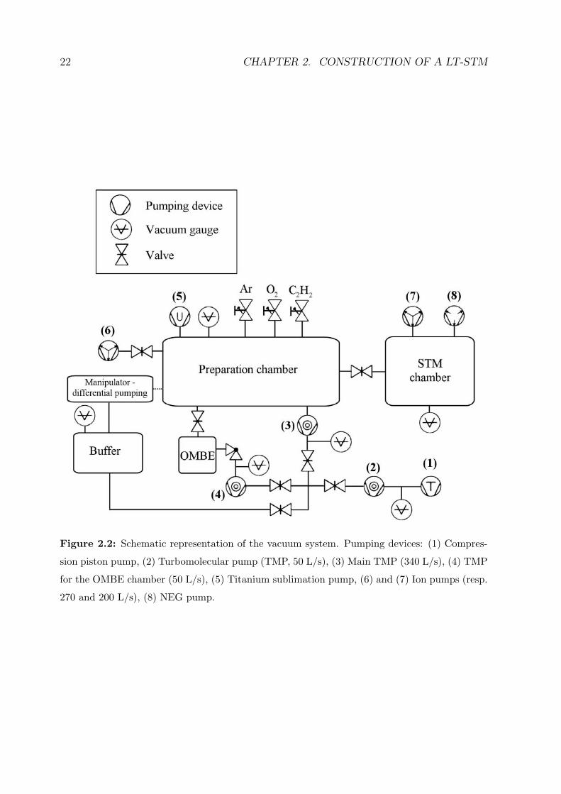
The vacuum chamber manufactured by the company VAb [101] is divided into two parts
(see figure 2.2): the preparation chamber, which consists in a horizontal cylinder 300 mm
in diameter, and the STM chamber, a vertical cylinder 350 mm in diameter. The two
parts are separated by a gate valve welded in the chamber. By closing this valve, the
sample preparation can be performed without contaminating the STM chamber, where
the cold STM and bath cryostat represent very efficient cold traps.
The pumping system
The whole chamber is pumped by a 340 L/s turbomolecular pump (TMP) with mag-
netic suspension [102]. In the ultra-high vacuum (UHV) regime, this pump can be turned
off to eliminate the (actually negligible) vibrations induced by its rotation mechanism,
22 CHAPTER 2. CONSTRUCTION OF A LT-STM
Figure 2.2: Schematic representation of the vacuum system. Pumping devices: (1) Compres-
sion piston pump, (2) Turbomolecular pump (TMP, 50 L/s), (3) Main TMP (340 L/s), (4) TMP
for the OMBE chamber (50 L/s), (5) Titanium sublimation pump, (6) and (7) Ion pumps (resp.
270 and 200 L/s), (8) NEG pump.
2.2. THE VACUUM CHAMBER 23
the pumping being in this case provided by two ion pumps, one at each chamber. To
increase the pumping capacity, a titanium sublimation pump (TSP) in the preparation
chamber and a non-evaporable getter (NEG) pump [103] in the STM chamber are in-
stalled. Pressures down to 1 × 10⁻¹⁰ mbar have been reached with this design. The
pressure even falls down when using the cryostat, as the large surface of the cold parts
acts as a very efficient cryo pump. It is thus believed that an excellent vacuum (well
below 10−10 mbar) is reached in the confined region of the sample and the STM in this
case. Pressures in the UHV parts are measured with two cold-cathode (Penning) gauges.
The forevacuum stage consists of a small 50 L/s turbomolecular pump in series with
an oil-free compression piston primary pump. A vacuum buffer of approximately 15 L
has been designed between this stage and the main turbomolecular pump. This allows to
shut down the primary pump, as it is the largest vibrational noise producing device, while
the main TMP is still working and ejecting the pumped gas into the buffer for a certain
time (up to 24 hours). The preparation of the next sample is in this way immediately
possible after a short STM measurement.
2.2.2 The preparation chamber
Instrumentation
The preparation chamber includes many flanges for installing various instruments and
future developments. Up to now, following devices are used:
An ion gun allows for bombarding the sample surface with argon ions of 500 to 1000 eV
kinetic energy in order to sputter out the first monolayers of the surface and therefore
remove the impurities. It requires an argon pressure of about 5×10⁻⁶ mbar in the chamber.
The gate valve to the STM chamber is closed during sputtering to avoid contamination.
A burst of titanium sublimation is usually performed just before operation in order to
purify the noble gas which is not pumped by titanium.
The Organic Molecular Beam Epitaxy (OMBE) source consists of a stainless-
steel crucible filled with the molecules to deposit (usually in powder form) and heated
to some hundreds of degrees (the sublimation temperature of the molecule), depending
on the material. In certain cases, it is necessary to use a gold-coated or a glass crucible
24 CHAPTER 2. CONSTRUCTION OF A LT-STM
in order to avoid catalytic cracking of the molecules before they sublimate. The source
contains two independent crucibles, is retractable and possesses an independent pumping
system so that it is possible to vent it, change the material, and pump it down again
without breaking the vacuum inside the main chamber.
An e-beam Molecular Beam Epitaxy (MBE) evaporator [104] is used for the
deposition of a precise amount of a metal species. This device is only suitable for certain
materials with high melting point, like Fe or Co. The material to deposit is in the form
of a metal rod, which is heated up by bombarding with an electron beam of typically a
few mA at an energy of up to 1 keV. This leads to the evaporation of minute quantities
from the top end of the rod.
Variable-leak valves allow admission of a controlled quantity (pressure) of gas for the
sample preparation or the study of its adsorption and reaction with the sample surface.
The Low Energy Electron Diffractometer (LEED) is a surface analysis tool to
investigate surface crystallographic structures. It is a simple and quick method to deter-
mine whether the sample surface is clean and well defined (i.e., well prepared) and whether
material has been deposited on it or not. Identification of adsorbate superstructures are
similarly possible.
A depot consisting of a linear feedthrough normal to the manipulator axis is included
in the STM chamber. It contains up to four samples in their sample holders. A fifth place
is kept for the tip changing tool (see figure 2.9). Two STM tip holders with their tips are
also stored in the depot.
A load-lock for a rapid exchange of samples and tips without breaking the vacuum has
been recently installed [105]. It can hold one sample and up to three tips.
Future implementations are planned allowing for example in situ irradiation of the
sample for the study of light-induced processes, or in situ deposition of metal species.

2.2. THE VACUUM CHAMBER 25
The sample holder
The manipulator (see Fig. 2.1) provides translational (600 mm along the chamber axis,
±25 mm in the two other directions) and rotational mobility (360) to position and
transfer the sample to the different preparation and measuring locations, as well as a
precise control of the sample temperature in the range 40-1400 K. The rotary feedthrough
requires a differential pumping which is obtained by a connection with the vacuum buffer
(Fig. 2.2).
Figure 2.3: The sample holder and the manipulator head: (1) Sample (single crystal), (2) Sam-
ple holder, (3) Thermocouple, (4) Filament for e-beam heating, (5) Holding fork, (6) Fixing arms,
(7) Translation rod to control the fixing arm position, (8) Return spring, (9) Insulating sapphire
plate, (10) Molybdenum support screwed on the flux cryostat cold plate (11).
The sample (1) (see figure 2.3) used is typically a metallic single crystal hat-like
shaped, 3 mm high and 7 mm in diameter. It is fixed in the sample holder (2) by a circlip

26 CHAPTER 2. CONSTRUCTION OF A LT-STM
made out of a tungsten ∅0.6 mm wire. A thermocouple type K (Chromel-Alumel) is posi-
tioned between the sample bottom and the circlip. Linking of the thermocouple between
sample holder and manipulator is obtained through the elastically shaped strips (3). The
latter are simply made out of a laminated ∅1 mm thermocouple wire.
The sample holder has two pairs of longitudinal grooves under it, the internal one
to maintain it on the manipulator, the external one to maintain it in the STM or in the
depot. Here the internal grooves fit onto the manipulator fork (5). The sample holder is
kept in position with the two arms (6) that can be opened or closed by translation of the
rod (7). The return spring (8) applies some stress in order to keep good thermal contact,
and prevents any damaging when heating or cooling down by taking over the thermal
stress.
Control of the sample temperature is twofold. On the one hand it can be cooled
by the manipulator head (10), connected to the cold plate (11) of a flux cryostat [106].
The temperature of the sample goes down to about 100 K when using liquid nitrogen,
and down to about 40 K when using liquid helium. On the other hand heating of the
sample is performed through the filament (4) located very close to the sample bottom.
For low power heating (counter-heating at low temperatures), the filament is heated up
by Joule effect and transfers radiational heat to the sample. For larger heating power, the
filament is additionally brought to a negative high voltage (700–1000 V) and produces
high energy electrons attracted to the nearest zero-potential part, i.e., the sample, to
which they deliver their heat converted energy. Temperatures of up to 1400 K can be
reached.
The sample holder, the fork and the fixing arms are electrically insulated, allowing for
the monitoring of the flowing electron current and thus the heating power. Insulation of
the fork (5) is obtained through sapphire plates (9) which are good thermal conductor at
low temperature; insulation of the arm (6) is obtained through standard ceramic parts.
All sample-holder metallic and ceramic custom parts were fabricated at the work-
shop of the Institute of Nanostructure Physics (IPN) of the Swiss Federal Institute of
Technology (EPFL). Sapphire parts were procured from the company Kyburz [107].
2.3. THE CRYOSTAT 27
Sample preparation
The experiments described in the following chapters were performed on various surface
orientations of noble-metal single crystals: Ag(100), Au(111), Cu(111) and Cu(100). They
were cleaned in situ under UHV conditions by sequential cycles of Ar+ sputtering at 300 K
(typically 20 minutes with a 5 µA/cm2 ion beam of 900 eV energy and an incident angle
of 45) and subsequent annealing (900 K for Cu and Au, and 700 K for Ag). The pressure
while annealing was always below 2 × 10⁻⁹ mbar. The procedure resulted in atomically
clean and flat surfaces with regions showing terraces of more than 100 nm in width.
The TPA molecules (from the company Fluka, purity >99%) were first outgassed in
vacuum for several hours and then evaporated from the OMBE cell at 150C onto the
substrate. This provides a deposition rate of about one monolayer (ML) per minute. For
the deposition of metal (Co and Fe) typically a deposition rate of 0.1 ML per minute was
used.
Tip preparation
The tips used are made out of a Platinum-Iridium (PtIr) alloy or Tungsten (W) ∅0.25 mm
wire. PtIr-tips are obtained by manual cutting and are directly usable. W tips are ob-
tained by electrochemical etching but usually oxidize and require in situ preparation, like
field emission treatment or ion bombardment [60–62]. The tip is magnetically maintained
in the STM by its tip holder and can be easily exchanged (see Fig. 2.9).
2.3 The cryostat
The bath cryostat, as designed by the company Cryovac [106], is shown schematically in
figure 2.4. It consists of a liquid helium tank (2) surrounded by a liquid nitrogen tank (1).
The STM is fixed on the cold plate (5). Nitrogen refill is needed every 60 hours (two days
and a half) whereas a helium filling lasts for more than three days.
Theoretical considerations
In vacuum, heat can be transmitted by conduction and radiation. The radiative power
emitted from a surface is proportional to the material emissivity and to the fourth power of
28 CHAPTER 2. CONSTRUCTION OF A LT-STM
Figure 2.4: Vertical cross section through the bath cryostat: (1) Liquid nitrogen tank (36 L),
(2) Liquid helium tank (9.3 L), (3) Feedthrough tube for the wires, (4) Radiation shield, (5) Cold
plate, (6) Suspension leg, (7) COF350 flange for fixing on the vacuum chamber.
the temperature: Prad = εAσ(T 4ext − T 4), where σ is the Stefan constant, A the radiative
area, ε the material emissivity, Text the surrounding temperature and T the material
temperature. For a fixed design (for a given A), it is therefore very efficient to place the low
temperature parts in a liquid nitrogen cooled environment, as going from a temperature
of 300 K down to 77 K (liquid nitrogen temperature) reduces the radiative power by a
factor of (300/77)4 ≈ 230. This is the purpose of the liquid nitrogen bath.
The surface of the cryostat is specially treated (polished or gold-plated) to enhance
its reflectivity in order to reduce the radiation absorption. The STM is screwed on the
cryostat cold plate ((5) Fig. 2.4). Directly around it a radiation shield (see figure 2.5)
kept at liquid helium temperature is mounted, surrounded by a second radiation shield
in thermal contact with the liquid nitrogen tank. The shields are made out of gold-
2.3. THE CRYOSTAT 29
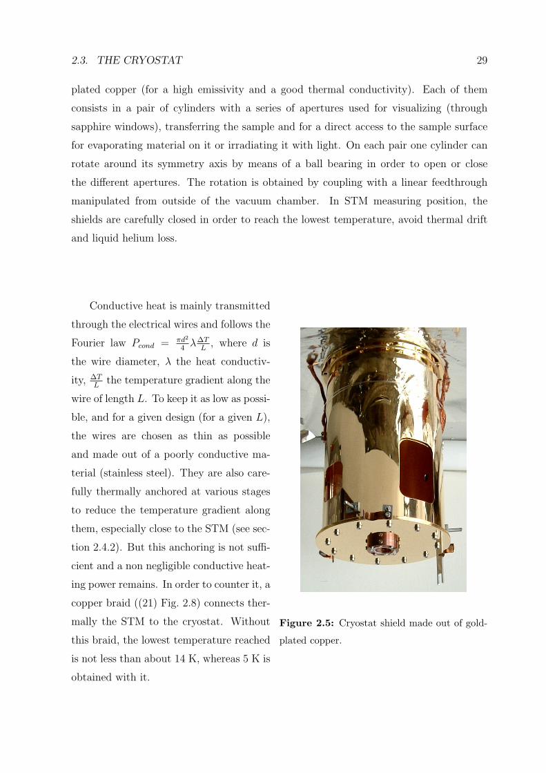
plated copper (for a high emissivity and a good thermal conductivity). Each of them
consists in a pair of cylinders with a series of apertures used for visualizing (through
sapphire windows), transferring the sample and for a direct access to the sample surface
for evaporating material on it or irradiating it with light. On each pair one cylinder can
rotate around its symmetry axis by means of a ball bearing in order to open or close
the different apertures. The rotation is obtained by coupling with a linear feedthrough
manipulated from outside of the vacuum chamber. In STM measuring position, the
shields are carefully closed in order to reach the lowest temperature, avoid thermal drift
and liquid helium loss.
Figure 2.5: Cryostat shield made out of gold-
plated copper.
Conductive heat is mainly transmitted
through the electrical wires and follows the
Fourier law Pcond = πd2
4λ∆T
L, where d is
the wire diameter, λ the heat conductiv-
ity, ∆TL
the temperature gradient along the
wire of length L. To keep it as low as possi-
ble, and for a given design (for a given L),
the wires are chosen as thin as possible
and made out of a poorly conductive ma-
terial (stainless steel). They are also care-
fully thermally anchored at various stages
to reduce the temperature gradient along
them, especially close to the STM (see sec-
tion 2.4.2). But this anchoring is not suffi-
cient and a non negligible conductive heat-
ing power remains. In order to counter it, a
copper braid ((21) Fig. 2.8) connects ther-
mally the STM to the cryostat. Without
this braid, the lowest temperature reached
is not less than about 14 K, whereas 5 K is
obtained with it.
30 CHAPTER 2. CONSTRUCTION OF A LT-STM
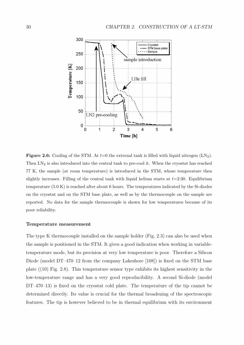
Figure 2.6: Cooling of the STM. At t=0 the external tank is filled with liquid nitrogen (LN2).
Then LN2 is also introduced into the central tank to pre-cool it. When the cryostat has reached
77 K, the sample (at room temperature) is introduced in the STM, whose temperature then
slightly increases. Filling of the central tank with liquid helium starts at t=2:30. Equilibrium
temperature (5.0 K) is reached after about 6 hours. The temperatures indicated by the Si-diodes
on the cryostat and on the STM base plate, as well as by the thermocouple on the sample are
reported. No data for the sample thermocouple is shown for low temperatures because of its
poor reliability.
Temperature measurement
The type K thermocouple installed on the sample holder (Fig. 2.3) can also be used when
the sample is positioned in the STM. It gives a good indication when working in variable-
temperature mode, but its precision at very low temperature is poor. Therefore a Silicon
Diode (model DT–470–12 from the company Lakeshore [108]) is fixed on the STM base
plate ((10) Fig. 2.8). This temperature sensor type exhibits its highest sensitivity in the
low-temperature range and has a very good reproducibility. A second Si-diode (model
DT–470–13) is fixed on the cryostat cold plate. The temperature of the tip cannot be
determined directly. Its value is crucial for the thermal broadening of the spectroscopic
features. The tip is however believed to be in thermal equilibrium with its environment
2.4. THE STM 31
because it is entirely surrounded by low-temperature parts and all the cables connected
to the scan piezo are properly thermalized (cf. sec. 2.4).
Cooling
The cooling down of the cryostat starts with the filling of the external tank with liquid
nitrogen (see figure 2.6). Before introducing liquid helium, the central tank is pre-cooled
with liquid nitrogen down to 77 K in order to avoid unnecessary use of liquid helium.
The equilibrium temperature is reached after a few hours. The Si-diode on the STM
plate indicates 5.0 K. The right positioning of the closed cryostat radiation shields is
crucial for the final temperature as well as for the liquid helium consumption. Any other
temperature between 5 K and 400 K can be reached by counter-heating with a Zener
diode (variable-temperature mode).
2.4 The STM
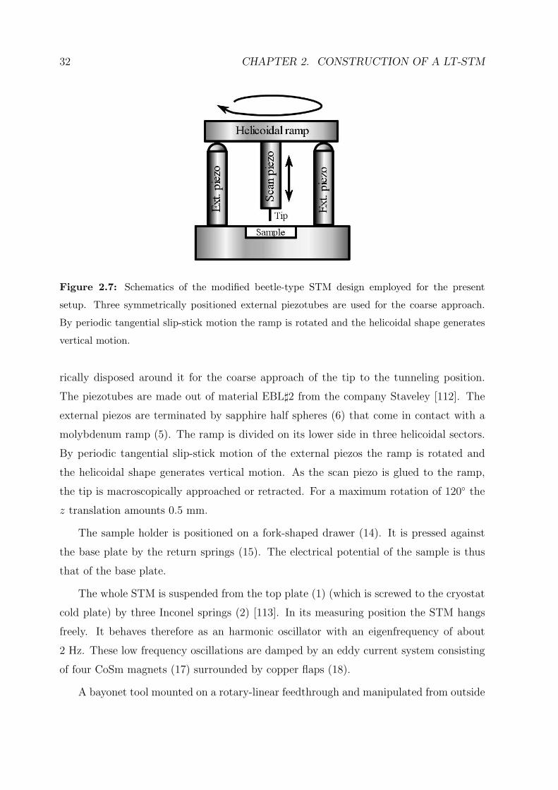
The design of the STM is based on the Besocke beetle type (figure 2.7) [109, 110]. This
design was adopted because of its relative simplicity and reliability, its compact size and
its mechanical stiffness, and because its symmetry makes it less susceptible to thermal
drift. The thermal dilatation of the scan piezo is indeed first-order compensated by the
external piezos. The difference with a standard Besocke type is that here the approach
ramp is located around the scan piezo and maintained by its own weight on the top of
the external piezos [90]. The sample is mounted in between the external piezos, what
provides good thermal contact between the sample and the STM base plate, an easier
access for transferring the sample, and more flexibility in the design of the sample holder.
All STM custom parts were fabricated at the workshop of the Institute of Nanostruc-
ture Physics (IPN) of the Swiss Federal Institute of Technology (EPFL). For the assembly
UHV-welding and gluing with UHV-compatible epoxy (Epo-tek H77 and H27D [111]) are
used.
2.4.1 Description
The STM is described in figure 2.8. It comprises a central piezo scantube (9) controlling
the tip position in x, y, and z directions, and three external piezo tubes (8) symmet-
32 CHAPTER 2. CONSTRUCTION OF A LT-STM
Figure 2.7: Schematics of the modified beetle-type STM design employed for the present
setup. Three symmetrically positioned external piezotubes are used for the coarse approach.
By periodic tangential slip-stick motion the ramp is rotated and the helicoidal shape generates
vertical motion.
rically disposed around it for the coarse approach of the tip to the tunneling position.
The piezotubes are made out of material EBL2 from the company Staveley [112]. The
external piezos are terminated by sapphire half spheres (6) that come in contact with a
molybdenum ramp (5). The ramp is divided on its lower side in three helicoidal sectors.
By periodic tangential slip-stick motion of the external piezos the ramp is rotated and
the helicoidal shape generates vertical motion. As the scan piezo is glued to the ramp,
the tip is macroscopically approached or retracted. For a maximum rotation of 120 the
z translation amounts 0.5 mm.
The sample holder is positioned on a fork-shaped drawer (14). It is pressed against
the base plate by the return springs (15). The electrical potential of the sample is thus
that of the base plate.
The whole STM is suspended from the top plate (1) (which is screwed to the cryostat
cold plate) by three Inconel springs (2) [113]. In its measuring position the STM hangs
freely. It behaves therefore as an harmonic oscillator with an eigenfrequency of about
2 Hz. These low frequency oscillations are damped by an eddy current system consisting
of four CoSm magnets (17) surrounded by copper flaps (18).
A bayonet tool mounted on a rotary-linear feedthrough and manipulated from outside
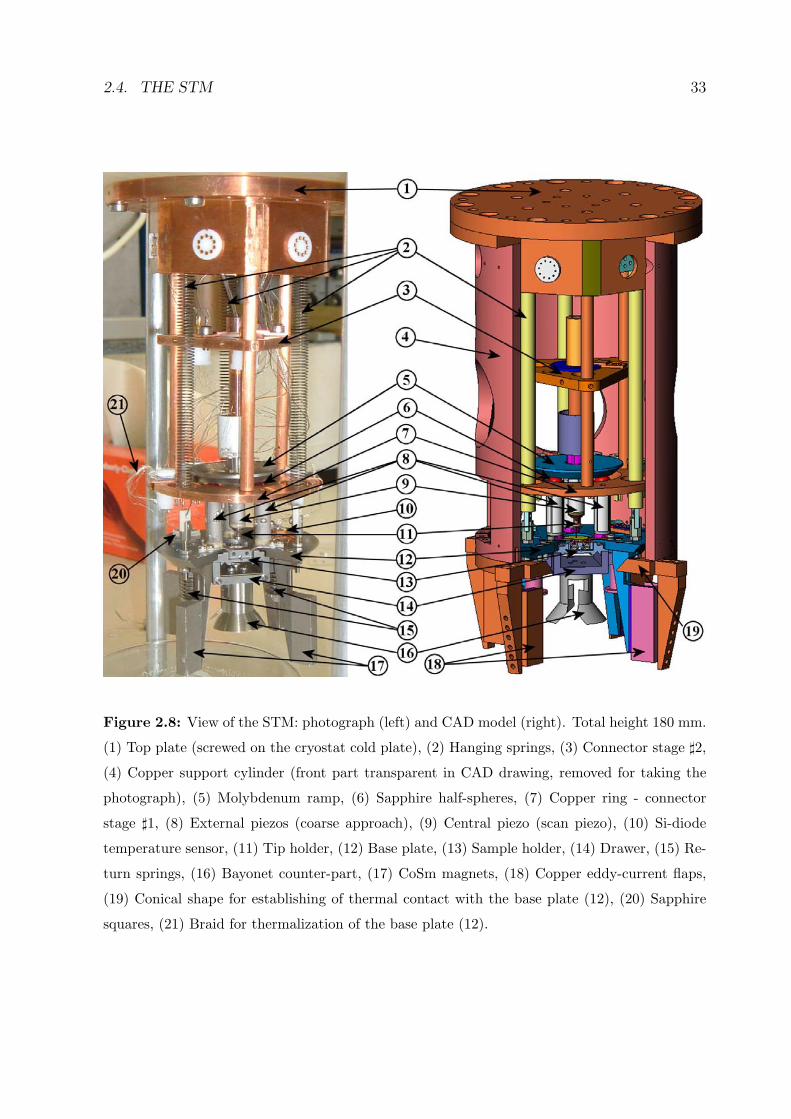
2.4. THE STM 33
Figure 2.8: View of the STM: photograph (left) and CAD model (right). Total height 180 mm.
(1) Top plate (screwed on the cryostat cold plate), (2) Hanging springs, (3) Connector stage 2,
(4) Copper support cylinder (front part transparent in CAD drawing, removed for taking the
photograph), (5) Molybdenum ramp, (6) Sapphire half-spheres, (7) Copper ring - connector
stage 1, (8) External piezos (coarse approach), (9) Central piezo (scan piezo), (10) Si-diode
temperature sensor, (11) Tip holder, (12) Base plate, (13) Sample holder, (14) Drawer, (15) Re-
turn springs, (16) Bayonet counter-part, (17) CoSm magnets, (18) Copper eddy-current flaps,
(19) Conical shape for establishing of thermal contact with the base plate (12), (20) Sapphire
squares, (21) Braid for thermalization of the base plate (12).
34 CHAPTER 2. CONSTRUCTION OF A LT-STM
of the vacuum chamber can be inserted in the counter-piece (16) in order to pull down
the STM. During this procedure the Mo-ramp (5) first sits on the copper ring (7), then
the base plate (12) comes in contact with the copper part (19). This position is ideal for
cooling down the STM, as the conical shape provides a non-negligible contact area and a
compressive stress can be applied. Furthermore the conical shape is self-centering, which
is important in particular to reposition the Mo-ramp, as it can swing macroscopically
in x and y directions. A further pull-down of the bayonet tool will compress the return
springs (15) (which are much stiffer that the springs (2)) and release the drawer (14) so
that the sample holder can be transferred to or out of the STM.
The STM is incorporated in a copper cylinder (4) providing some holes for direct access
from the outside. The purpose of this part is to maintain the eddy current flaps (18), and
to establish good thermal and mechanical contact with the base plate (12) via the conical
shape (19) when it is in the cooling or transferring position.
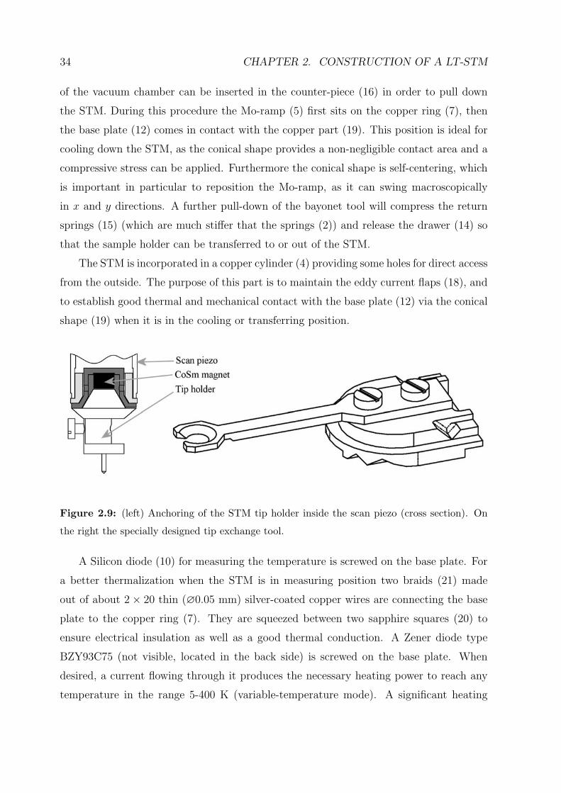
Figure 2.9: (left) Anchoring of the STM tip holder inside the scan piezo (cross section). On
the right the specially designed tip exchange tool.
A Silicon diode (10) for measuring the temperature is screwed on the base plate. For
a better thermalization when the STM is in measuring position two braids (21) made
out of about 2 × 20 thin (∅0.05 mm) silver-coated copper wires are connecting the base
plate to the copper ring (7). They are squeezed between two sapphire squares (20) to
ensure electrical insulation as well as a good thermal conduction. A Zener diode type
BZY93C75 (not visible, located in the back side) is screwed on the base plate. When
desired, a current flowing through it produces the necessary heating power to reach any
temperature in the range 5-400 K (variable-temperature mode). A significant heating
2.4. THE STM 35
power is obtained with a relatively low current because of the high threshold potential of
the diode (75 V).
The tip holder (11) made out of steel is maintained in position inside the central piezo
by a CoSm magnet. Tips can therefore be exchanged or treated in situ. For this purpose
a specially designed tip exchange tool is used (see figure 2.9).
2.4.2 Wiring
The requirements needed for a proper wiring of the STM head are listed below.
Around the STM: The main requirement for the wires connected directly to the STM
is a high flexibility for avoiding the transmission of vibrations. Kapton coated
∅50 µm copper wires are used. 23 cables are connected to connector stage 1, 9 to
connector stage 2 (figure 2.8). This second stage delivers all the signals for the cen-
tral piezo. Special connectors made with sapphires plates are used here to ensure
proper thermalization of the cables and therefore of the entire piezo (especially the
tip). The connectors are positioned for an easy mounting/dismounting of the base
plate and the central piezo. A last set of connectors on the top plate ((1) Fig. 2.8)
allows for dismounting of the whole STM out of the cryostat.
Inside the cryostat: Here the thermal properties are decisive. The heat conducted
from the room temperature parts to the liquid helium temperature core must be
minimized. A poor conductive material is used (stainless steel, teflon coated [114])
in combination with a rather small diameter (0.1 mm). To avoid electromagnetical
noise coaxial cables are necessary for the tunneling current, the sample bias, and the
z-electrode signals. The capacitance of the coaxial cables is of great importance as
it will set the upper limit for the frequency response of the feedback loop. Coaxial
cables type SS from the company Lakeshore [108] are used (∅1 mm, capacitance
0.17 nF/m). Phosphor-bronze twisted wire pairs are used to minimize the pickup
noise for the four-points temperature measurement of the Si-diodes.
Thermal anchoring consisting in winding around heat sinks is implemented for all
the cables at the bottom of the liquid helium tank (at 4.2 K) as well as above it
at ∼20 K. In between, the cables are passing in the feedthrough tubes (3) of Fig. 2.4
36 CHAPTER 2. CONSTRUCTION OF A LT-STM
through the liquid helium tank.
Outside of the vacuum chamber: Here standard cables are used. Coaxial BNC ca-
bles are connecting all the scan piezo electrodes, as well as the sample bias. The
tunneling current preamplifier is connected directly at the exit of the vacuum cham-
ber.
2.4.3 Mechanical stability
STM measurements require a great stability (the resolution in z must be <0.01 A). It is
therefore crucial to know the mechanical characteristics of the STM head and its frequency
dependent behavior, and to get rid of external vibrations by use of appropriate damping.
The external noise sources are principally the building oscillations and the acoustic waves.
Building oscillations are typically in the range 1 to 30 Hz and are partially damped
(figure 2.10) by the pneumatic legs holding the whole apparatus (see Fig. 2.1). The
second pneumatic isolator stage ((6) Fig. 2.4) decouples further the He-bath cryostat and
limits transmission of eigenfrequencies from the rest of the vacuum chamber, as well as the
vibrations coming from the bubbling of liquid nitrogen. The STM itself is then held on
three springs that act as a low-pass filter with an eigenfrequency of about 2 Hz. To prevent
long time oscillations at this frequency, eddy current damping is installed (figure 2.8).
Calculation of eigenfrequencies
The beetle-type STM can be modeled as a disk of mass M sitting on three massless piezo
tubes (see Fig. 2.7) with spring constants K⊥ and K‖ for bending and stretching motions,
respectively. For a tube with length l, inner diameter d, outer diameter D, and Young
modulus E, the spring constants are [115]:
K⊥ =3π
64E
D4 − d4
l3and K‖ =
π
4E
D2 − d2
l
If we assume that the legs are fixed to the ramp we can calculate the resonance
frequency for the three different modes horizontal translation (H), vertical translation (V )
2.4. THE STM 37
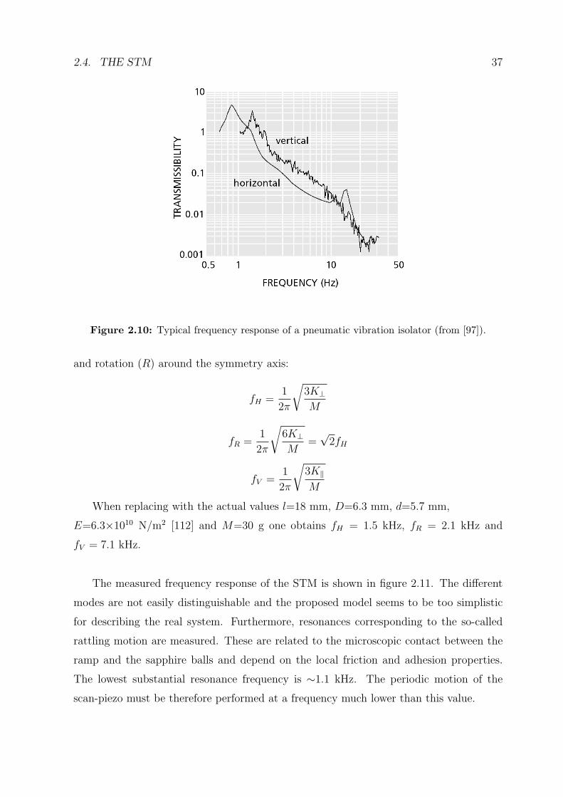
Figure 2.10: Typical frequency response of a pneumatic vibration isolator (from [97]).
and rotation (R) around the symmetry axis:
fH =1
2π
√3K⊥M
fR =1
2π
√6K⊥M
=√
2fH
fV =1
2π
√3K‖M
When replacing with the actual values l=18 mm, D=6.3 mm, d=5.7 mm,
E=6.3×10¹⁰ N/m2 [112] and M=30 g one obtains fH = 1.5 kHz, fR = 2.1 kHz and
fV = 7.1 kHz.
The measured frequency response of the STM is shown in figure 2.11. The different
modes are not easily distinguishable and the proposed model seems to be too simplistic
for describing the real system. Furthermore, resonances corresponding to the so-called
rattling motion are measured. These are related to the microscopic contact between the
ramp and the sapphire balls and depend on the local friction and adhesion properties.
The lowest substantial resonance frequency is ∼1.1 kHz. The periodic motion of the
scan-piezo must be therefore performed at a frequency much lower than this value.
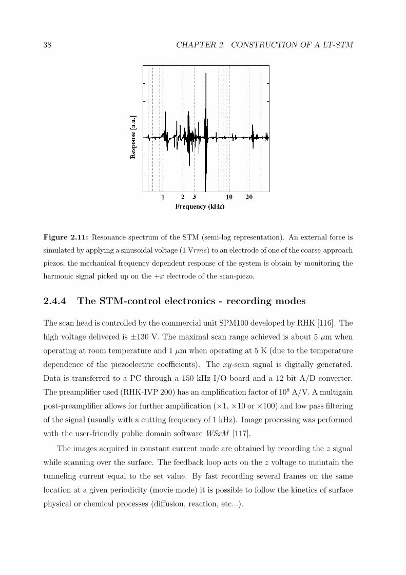
38 CHAPTER 2. CONSTRUCTION OF A LT-STM
Figure 2.11: Resonance spectrum of the STM (semi-log representation). An external force is
simulated by applying a sinusoidal voltage (1 Vrms) to an electrode of one of the coarse-approach
piezos, the mechanical frequency dependent response of the system is obtain by monitoring the
harmonic signal picked up on the +x electrode of the scan-piezo.
2.4.4 The STM-control electronics - recording modes
The scan head is controlled by the commercial unit SPM100 developed by RHK [116]. The
high voltage delivered is ±130 V. The maximal scan range achieved is about 5 µm when
operating at room temperature and 1 µm when operating at 5 K (due to the temperature
dependence of the piezoelectric coefficients). The xy-scan signal is digitally generated.
Data is transferred to a PC through a 150 kHz I/O board and a 12 bit A/D converter.
The preamplifier used (RHK-IVP 200) has an amplification factor of 108 A/V. A multigain
post-preamplifier allows for further amplification (×1, ×10 or ×100) and low pass filtering
of the signal (usually with a cutting frequency of 1 kHz). Image processing was performed
with the user-friendly public domain software WSxM [117].
The images acquired in constant current mode are obtained by recording the z signal
while scanning over the surface. The feedback loop acts on the z voltage to maintain the
tunneling current equal to the set value. By fast recording several frames on the same
location at a given periodicity (movie mode) it is possible to follow the kinetics of surface
physical or chemical processes (diffusion, reaction, etc...).
2.5. STM TEST MEASUREMENTS 39
For spectroscopy measurements the tip is moved to the desired location and the
feedback loop is opened, so that the tip position is kept constant. The bias voltage is
then ramped. The tunneling current is recorded and its numerical derivative with respect
to the bias voltage delivers the requested dI/dV spectrum. Another possibility is to add
a small ac modulation in the bias voltage at a given frequency. By means of a lock-in
amplifier the related harmonics in the tunneling current are extracted. The first harmonic
is proportional to dI/dV , and the second to d2I/dV 2.
2.5 STM test measurements
The first measurements performed with the new experimental setup described in this
chapter demonstrate its ability to investigate surfaces with high resolution. In particular,
the observation of the very low corrugated standing waves on Au(111) is a confirmation
of the overall excellent stability of the STM down to a temperature of 5 K.
Atomic resolution on Ag(100)
Figure 2.12 is a STM image of a Ag(100) surface revealing atomic resolution and the
corresponding square crystallographic structure. The atomic corrugation is about ≈0.1 A,
the noise amplitude is close to 0.03 A.
Surface states on Au(111)
Densely packed fcc(111) noble metal surfaces exhibit Shockley-type surface states. These
electronic states are located energetically in the partial gap of the bulk states. Their wave
functions peak near the surface and decay exponentially both into the vacuum and into
the bulk of the solid. Parallel to the surface they behave as a two-dimensional (2D) free
electron gas characterized by k‖, the wave vector parallel to the surface. The surface-
state dispersion is thus expected to be parabolic and isotropic in the center of the surface
Brillouin zone Γ:
E = EΓ +
2
2m∗k2‖. (2.1)
Here EΓ is the surface-state band edge energy and m∗ the effective mass. The density of
states of a free 2D electron gas is a constant above the onset at EΓ.
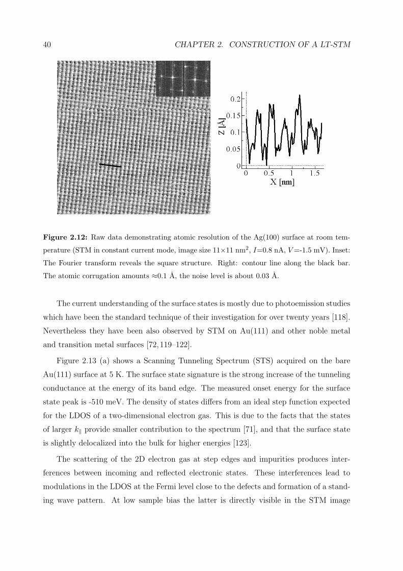
40 CHAPTER 2. CONSTRUCTION OF A LT-STM
Figure 2.12: Raw data demonstrating atomic resolution of the Ag(100) surface at room tem-
perature (STM in constant current mode, image size 11×11 nm2, I=0.8 nA, V =-1.5 mV). Inset:
The Fourier transform reveals the square structure. Right: contour line along the black bar.
The atomic corrugation amounts ≈0.1 A, the noise level is about 0.03 A.
The current understanding of the surface states is mostly due to photoemission studies
which have been the standard technique of their investigation for over twenty years [118].
Nevertheless they have been also observed by STM on Au(111) and other noble metal
and transition metal surfaces [72,119–122].
Figure 2.13 (a) shows a Scanning Tunneling Spectrum (STS) acquired on the bare
Au(111) surface at 5 K. The surface state signature is the strong increase of the tunneling
conductance at the energy of its band edge. The measured onset energy for the surface
state peak is -510 meV. The density of states differs from an ideal step function expected
for the LDOS of a two-dimensional electron gas. This is due to the facts that the states
of larger k‖ provide smaller contribution to the spectrum [71], and that the surface state
is slightly delocalized into the bulk for higher energies [123].
The scattering of the 2D electron gas at step edges and impurities produces inter-
ferences between incoming and reflected electronic states. These interferences lead to
modulations in the LDOS at the Fermi level close to the defects and formation of a stand-
ing wave pattern. At low sample bias the latter is directly visible in the STM image
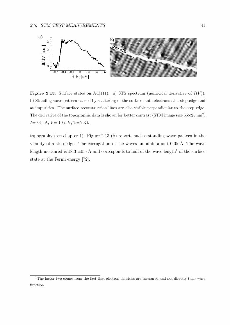
2.5. STM TEST MEASUREMENTS 41
Figure 2.13: Surface states on Au(111). a) STS spectrum (numerical derivative of I(V )).
b) Standing wave pattern caused by scattering of the surface state electrons at a step edge and
at impurities. The surface reconstruction lines are also visible perpendicular to the step edge.
The derivative of the topographic data is shown for better contrast (STM image size 55×25 nm2,
I=0.4 nA, V =-10 mV, T=5 K).
topography (see chapter 1). Figure 2.13 (b) reports such a standing wave pattern in the
vicinity of a step edge. The corrugation of the waves amounts about 0.05 A. The wave
length measured is 18.3 ±0.5 A and corresponds to half of the wave length1 of the surface
state at the Fermi energy [72].
1The factor two comes from the fact that electron densities are measured and not directly their wave
function.

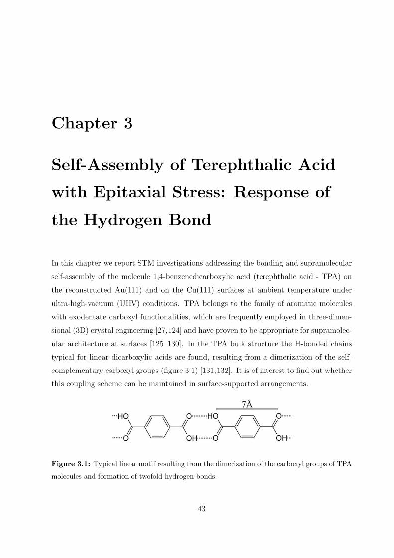
Chapter 3
Self-Assembly of Terephthalic Acid
with Epitaxial Stress: Response of
the Hydrogen Bond
In this chapter we report STM investigations addressing the bonding and supramolecular
self-assembly of the molecule 1,4-benzenedicarboxylic acid (terephthalic acid - TPA) on
the reconstructed Au(111) and on the Cu(111) surfaces at ambient temperature under
ultra-high-vacuum (UHV) conditions. TPA belongs to the family of aromatic molecules
with exodentate carboxyl functionalities, which are frequently employed in three-dimen-
sional (3D) crystal engineering [27,124] and have proven to be appropriate for supramolec-
ular architecture at surfaces [125–130]. In the TPA bulk structure the H-bonded chains
typical for linear dicarboxylic acids are found, resulting from a dimerization of the self-
complementary carboxyl groups (figure 3.1) [131,132]. It is of interest to find out whether
this coupling scheme can be maintained in surface-supported arrangements.
Figure 3.1: Typical linear motif resulting from the dimerization of the carboxyl groups of TPA
molecules and formation of twofold hydrogen bonds.
43
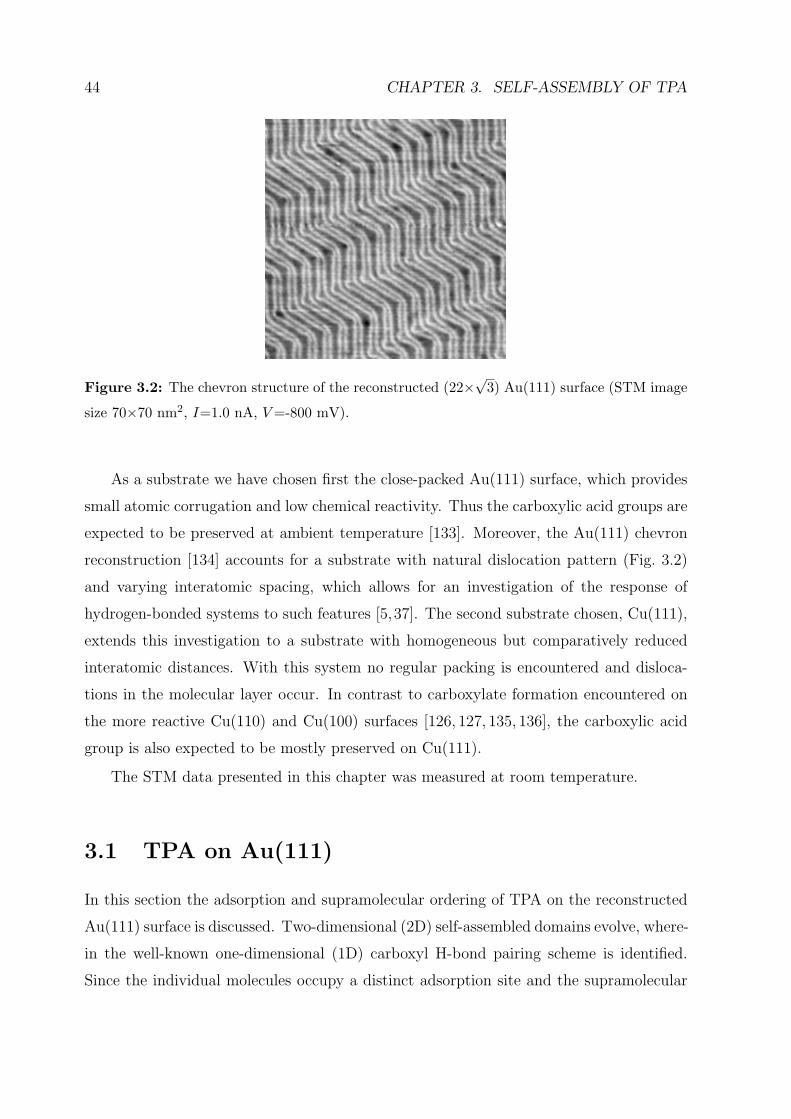
44 CHAPTER 3. SELF-ASSEMBLY OF TPA
Figure 3.2: The chevron structure of the reconstructed (22×√3) Au(111) surface (STM image
size 70×70 nm2, I=1.0 nA, V =-800 mV).
As a substrate we have chosen first the close-packed Au(111) surface, which provides
small atomic corrugation and low chemical reactivity. Thus the carboxylic acid groups are
expected to be preserved at ambient temperature [133]. Moreover, the Au(111) chevron
reconstruction [134] accounts for a substrate with natural dislocation pattern (Fig. 3.2)
and varying interatomic spacing, which allows for an investigation of the response of
hydrogen-bonded systems to such features [5,37]. The second substrate chosen, Cu(111),
extends this investigation to a substrate with homogeneous but comparatively reduced
interatomic distances. With this system no regular packing is encountered and disloca-
tions in the molecular layer occur. In contrast to carboxylate formation encountered on
the more reactive Cu(110) and Cu(100) surfaces [126, 127, 135, 136], the carboxylic acid
group is also expected to be mostly preserved on Cu(111).
The STM data presented in this chapter was measured at room temperature.
3.1 TPA on Au(111)
In this section the adsorption and supramolecular ordering of TPA on the reconstructed
Au(111) surface is discussed. Two-dimensional (2D) self-assembled domains evolve, where-
in the well-known one-dimensional (1D) carboxyl H-bond pairing scheme is identified.
Since the individual molecules occupy a distinct adsorption site and the supramolecular
3.1. TPA ON AU(111) 45
ordering usually extends over several substrate reconstruction domains, the inhomoge-
neous distortions of the latter induce significant variations in hydrogen bond lengths,
which illustrates the versatility of hydrogen bridges in molecular engineering at surfaces.
Ab initio calculations for a 1D H-bonded molecular chain provide insight into the limited
geometric response of the molecules in different local environments. At small concen-
trations adsorbed TPA is highly mobile and induces an increased mobility of substrate
atomic steps.
3.1.1 Description of the self-assembly
Samples with a coverage of one monolayer or less were prepared. One monolayer (ML)
refers to a complete layer of the dense hydrogen-bonded phase described below. At small
concentrations it is difficult to determine the exact coverage by STM at room temperature
because the molecules are very mobile on the gold surface and form a two-dimensional
molecular gas phase where the molecules cannot be imaged individually. Upon increas-
ing the density beyond about 0.5 ML the molecules condense into large compact well
ordered domains. However, these domains can be easily perturbed by lowering the tunnel
resistance (approximately under 10 MΩ).
The adsorption of aromatic molecules on transition and noble metal surfaces is mainly
directed by the interaction of the π-orbitals of the aromatic ring with the d-orbitals of the
substrate (see, e.g., Ref. [137]). On Au(111), the physisorption of TPA is strong enough to
keep the molecules on the surface up to about 430 K, the temperature at which they start
to desorb. This temperature corresponds to an activation energy for desorption of roughly
1 eV [138]. For comparison, the adsorption energy of benzene on Au(111) amounts 0.6 eV
(60 kJ/mol) [139]. However, the surface diffusion barrier of TPA is low and therefore the
molecular diffusivity is high at room temperature. It should be pointed out that, although
the substrate appears thus rather flat with regard to the 2D diffusion, the modulations
in the surface potential due to the atomic periodicity are sufficiently strong to determine
the commensurability of the adsorbed supramolecular sheet, as we will show below.
Figure 3.3 shows the typical organization of a TPA layer. The chevron reconstruc-
tion of the Au(111) surface [134] is clearly visible in the upper part, where very mobile
molecules are present, as well as in the lower part underneath the TPA layer. The layer
imaging height is 0.8±0.1 A above the surface covered by the 2D gas phase, the intralayer
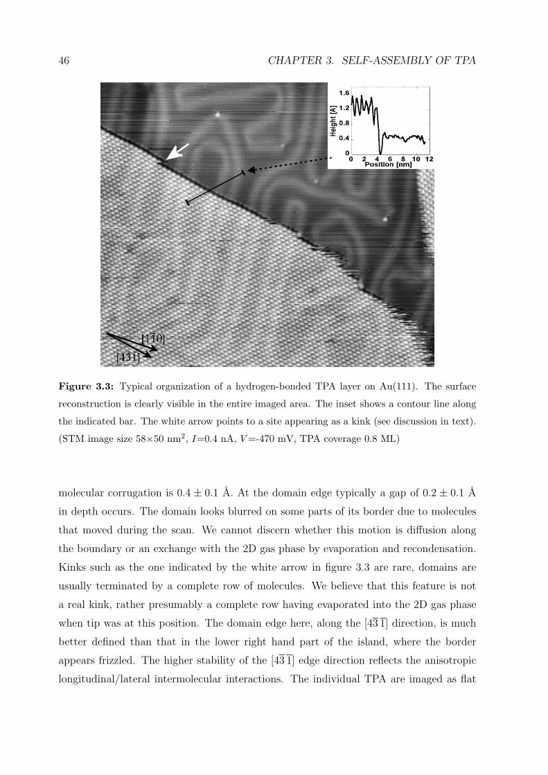
46 CHAPTER 3. SELF-ASSEMBLY OF TPA
Figure 3.3: Typical organization of a hydrogen-bonded TPA layer on Au(111). The surface
reconstruction is clearly visible in the entire imaged area. The inset shows a contour line along
the indicated bar. The white arrow points to a site appearing as a kink (see discussion in text).
(STM image size 58×50 nm2, I=0.4 nA, V =-470 mV, TPA coverage 0.8 ML)
molecular corrugation is 0.4 ± 0.1 A. At the domain edge typically a gap of 0.2 ± 0.1 A
in depth occurs. The domain looks blurred on some parts of its border due to molecules
that moved during the scan. We cannot discern whether this motion is diffusion along
the boundary or an exchange with the 2D gas phase by evaporation and recondensation.
Kinks such as the one indicated by the white arrow in figure 3.3 are rare, domains are
usually terminated by a complete row of molecules. We believe that this feature is not
a real kink, rather presumably a complete row having evaporated into the 2D gas phase
when tip was at this position. The domain edge here, along the [43 1] direction, is much
better defined than that in the lower right hand part of the island, where the border
appears frizzled. The higher stability of the [43 1] edge direction reflects the anisotropic
longitudinal/lateral intermolecular interactions. The individual TPA are imaged as flat
3.1. TPA ON AU(111) 47
rod-like protrusions (about 7 A×5 A) aligned with the [43 1] direction. Their dimension is
fitting well with the size of a flat lying molecule. The observation of a preferred direction
both on an individual molecular basis and arising from the domain stability determines
the orientation of the molecules relative to each other, which is governed by the carboxylic
acid dimerization via hydrogen bonding, as expected from the shape and functionality of
the molecule (figure 3.1). The formation of 2D molecular sheets furthermore suggests
a lateral coupling between the 1D TPA chains, which is presumably mediated by weak
hydrogen bonds or electrostatic interactions. The observed structure is similar to the one
of TPA bulk and in agreement with investigations of related systems [11, 125, 127, 128].
Apart from the reconstruction pattern of the underlying gold substrate no long range
corrugation (indicative of a Moire or a dislocation pattern) of the TPA sheets could be
seen. Therefore we deduce that the molecular layer is commensurate with the substrate
and that the individual TPA reside at a distinct adsorption site. The actual adsorption
site could not be identified on the basis of the present experiments.
The TPA molecules arrange in a quasi-hexagonal lattice with different orientations
relative to the substrate. Figure 3.4 shows four coexisting rotational domains. The
rectangular shape delimiting a region covered by the 2D gas phase is at first glance
unexpected on a surface with hexagonal symmetry but can be easily explained by the
molecular superstructure. We observed in total six equivalent orientational domains. The
unit cell parameters measured are 8.3±0.3 A (along [011]) and 10.0±0.3 A with an angle
of 45 ± 3. The quasi right angle between the domains thus results from two adjacent
mirror domains leading to an overall rotation of the molecular chains by 2 × 45.
We propose the following matrices to describe the commensurate superstructure: 3 0
1 3
and its mirror symmetry
3 −3
−2 −1
. Note that this superstructure is re-
ferred to an ideal (111) plane; the exact superstructure matrix should also include the
(22×√3) gold reconstruction. Figure 3.5 shows the proposed model for the unit cell. For
simplicity we first consider the Au(111) surface plane as perfectly hexagonal (as the sur-
face is reconstructed this is not exactly true; this point will be discussed below). Three
rotational domains exist reflecting the substrate symmetry. In addition, since the molecu-
lar lattice is not exactly hexagonal, within each rotational domain two chiral arrangements
related by a mirror symmetry exist. The molecule itself is not chiral, neither in the gas
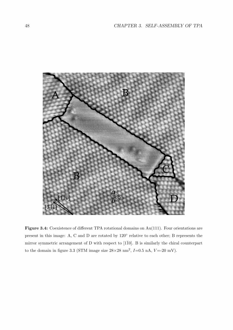
48 CHAPTER 3. SELF-ASSEMBLY OF TPA
Figure 3.4: Coexistence of different TPA rotational domains on Au(111). Four orientations are
present in this image: A, C and D are rotated by 120 relative to each other; B represents the
mirror symmetric arrangement of D with respect to [110]. B is similarly the chiral counterpart
to the domain in figure 3.3 (STM image size 28×28 nm2, I=0.5 nA, V =-20 mV).
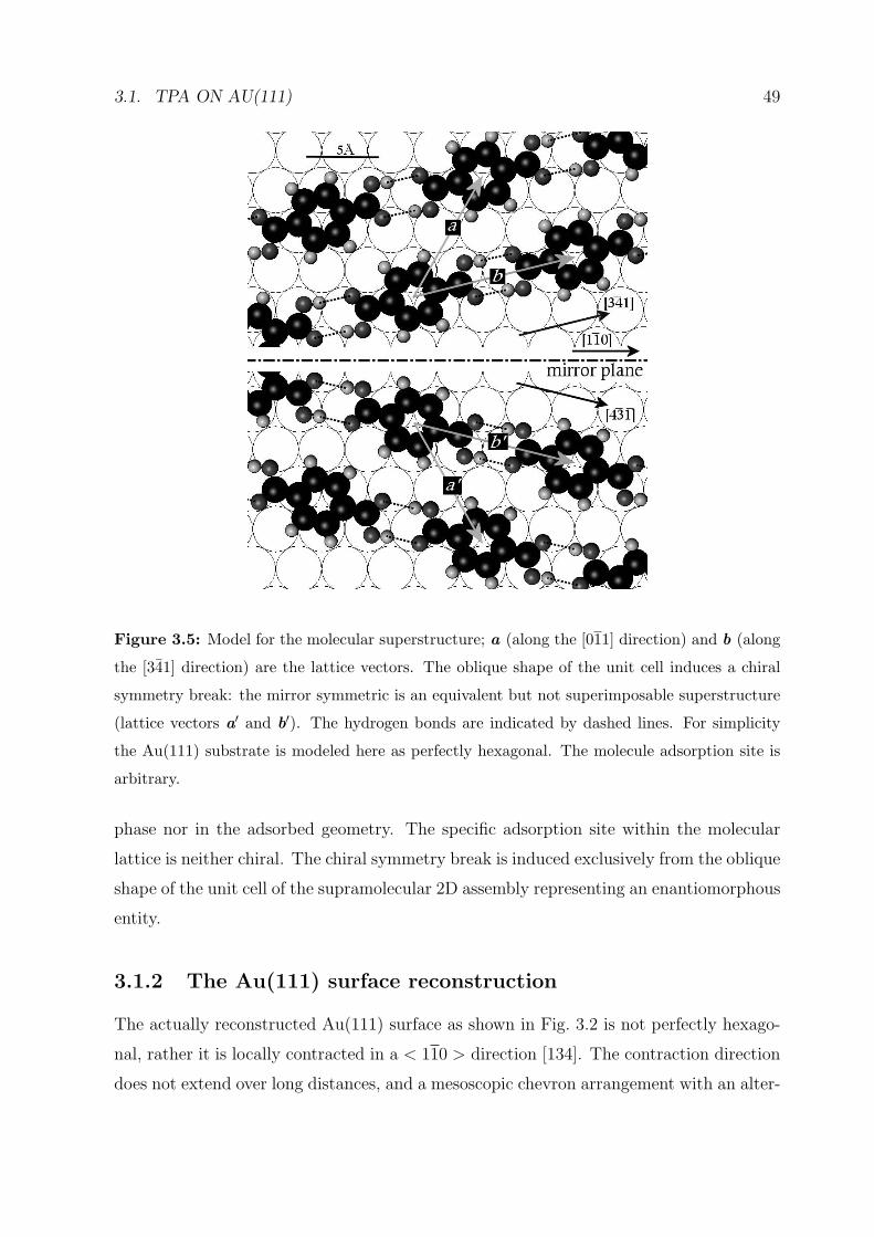
3.1. TPA ON AU(111) 49
Figure 3.5: Model for the molecular superstructure; a (along the [011] direction) and b (along
the [341] direction) are the lattice vectors. The oblique shape of the unit cell induces a chiral
symmetry break: the mirror symmetric is an equivalent but not superimposable superstructure
(lattice vectors a′ and b′). The hydrogen bonds are indicated by dashed lines. For simplicity
the Au(111) substrate is modeled here as perfectly hexagonal. The molecule adsorption site is
arbitrary.
phase nor in the adsorbed geometry. The specific adsorption site within the molecular
lattice is neither chiral. The chiral symmetry break is induced exclusively from the oblique
shape of the unit cell of the supramolecular 2D assembly representing an enantiomorphous
entity.
3.1.2 The Au(111) surface reconstruction
The actually reconstructed Au(111) surface as shown in Fig. 3.2 is not perfectly hexago-
nal, rather it is locally contracted in a < 110 > direction [134]. The contraction direction
does not extend over long distances, and a mesoscopic chevron arrangement with an alter-
50 CHAPTER 3. SELF-ASSEMBLY OF TPA
nating sequence of two rotational domains occurs at large terraces [134,140,141]. As the
intermolecular distance is much smaller than the extension of these domains the molec-
ular superstructure should be influenced by the distorted surface (analogous to simple
superlattices on reconstructed Au(111), see [142]).
Figure 3.6: Model showing the atomic positions of the surface layer on Au(111) and the
(22×√3) unit cell; small circles: atoms of the second layer; large circles: atoms of the top layer;
white: transition region (corrugation lines).
Description
The uniaxial contraction results in a (22×√3) unit cell where surface Au atoms reside
on fcc, hcp and bridge-type stacking positions on the second layer. The corrugation lines
separate the fcc from the hcp regions (figure 3.6). The distance between two adjacent lines
is 44 A, the neighbored line pairs are 63 A apart. The reconstruction corrugation typically
amounts up to 0.2 A over a distance of 442
A, which gives an out-of-plane correction of
about 0.5. The fcc to hcp site modulation produces a curvature in the lateral atomic
alignment of the order of 0.8 A over a distance of 632
A, which gives an in-plane correction
of about 1.5. These two effects give a correction for the intermolecular distances in the
adsorbed layer of the order of a(1 − cos α) ≈0.5 pm and are neglected.
Therefore we model the reconstructed surface as a uniaxially and homogeneously
contracted hexagonal plane. In the contraction direction we take a constant interatomic
distance of 2.75 A (the bulk interatomic distance is 2.88 A). Note that in reality this
distance oscillates around this value with an amplitude of ±0.1 A over the period of the
reconstruction (23 surface atomic spacings). In the two other close-packed directions the
interatomic distance is assumed to be 2.85 A.
3.1. TPA ON AU(111) 51
Figure 3.7: The effect of the Au(111) substrate reconstruction on the molecular lattice, and
the dependance on the contraction direction. In grey is shown the molecular cell corresponding
to a perfectly hexagonal substrate, in black the molecular cell uniaxially contracted along the
direction indicated by the double arrow. The type numbers refer to table 3.1.
Influence on the molecular layer
The distortion of the reconstructed surface is transmitted into the molecular lattice, as
shown schematically in figure 3.7. Depending on its orientation relative to the surface
contraction direction, we find three different unit cells, labeled type 1, 2 and 3, whose
parameters are indicated in table 3.1. Although these differences are close to the exper-
imental error we could find direct evidence. Figure 3.8 shows a single molecular domain
extending over two gold reconstruction domains. The upper region of the domain is of
type 1 while the lower region is of type 2. As shown in the Fourier transform of the two
regions, the respective lattice parameters have distinct differences. To explain these dif-
ferences in more details, the molecular domains are modeled in figure 3.9. The contraction
direction, varying from [110] to [101] influences directly the intermolecular distances (and
the hydrogen bond lengths), and induces also small differences in the lattice orientation.
We never obtained sufficiently high resolution in the STM images to resolve the in-
dividual functional groups of the molecule. This is generally the case in UHV stud-
ies, in agreement with the current theoretical understanding in STM imaging of organic
52 CHAPTER 3. SELF-ASSEMBLY OF TPA
Figure 3.8: Left: STM image of a single molecular domain extending over two substrate re-
construction domains. The respective contraction directions are indicated by the double arrows.
(image size 35×22 nm2, I=0.4 nA, V =-400 mV). Right: Fourier transform of the two regions
marked 1 and 2, corresponding to the two orientations of the reconstruction detailed in table 3.1
and modeled in figure 3.9. While the intermolecular coupling scheme is maintained in the entire
molecular layer, it adapts locally to the reconstructed gold lattice so that slightly different unit
cell parameters are found in the two regions. Note that the Fourier image refers to the center of
the spots which are in reality smeared because - apart from the experimental error - the local
variations of the contracted interatomic distance around its mean value induces local variations
of the intermolecular distances up to a few %.
3.1. TPA ON AU(111) 53
Figure 3.9: Model showing the effect of the uniaxial contraction of the (22×√3) reconstruction
on the molecular superlattice. Note the differences in the H-bond lengths and in the molecular
orientation. Domain types (1) and (2) correspond to those in table 3.1 and in the STM image of
figure 3.8. The substrate atomic distances are greatly exaggerated to emphasize the differences
in the molecular lattice. The contraction direction is indicated by a double arrow ([110] in
domain (1), [101] in domain (2)). The complex structure of the substrate domain boundary is
not represented.
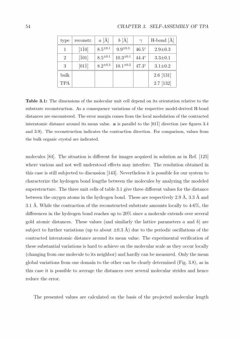
54 CHAPTER 3. SELF-ASSEMBLY OF TPA
type reconstr. a [A] b [A] γ H-bond [A]
1 [110] 8.5±0.1 9.9±0.3 46.5 2.9±0.3
2 [101] 8.5±0.1 10.3±0.1 44.4 3.3±0.1
3 [011] 8.2±0.3 10.1±0.2 47.3 3.1±0.2
bulk 2.6 [131]
TPA 2.7 [132]
Table 3.1: The dimensions of the molecular unit cell depend on its orientation relative to the
substrate reconstruction. As a consequence variations of the respective model-derived H-bond
distances are encountered. The error margin comes from the local modulation of the contracted
interatomic distance around its mean value. a is parallel to the [011] direction (see figures 3.4
and 3.9). The reconstruction indicates the contraction direction. For comparison, values from
the bulk organic crystal are indicated.
molecules [84]. The situation is different for images acquired in solution as in Ref. [125]
where various and not well understood effects may interfere. The resolution obtained in
this case is still subjected to discussion [143]. Nevertheless it is possible for our system to
characterize the hydrogen bond lengths between the molecules by analyzing the modeled
superstructure. The three unit cells of table 3.1 give three different values for the distance
between the oxygen atoms in the hydrogen bond. These are respectively 2.9 A, 3.3 A and
3.1 A. While the contraction of the reconstructed substrate amounts locally to 4-6%, the
differences in the hydrogen bond reaches up to 20% since a molecule extends over several
gold atomic distances. These values (and similarly the lattice parameters a and b) are
subject to further variations (up to about ±0.3 A) due to the periodic oscillations of the
contracted interatomic distance around its mean value. The experimental verification of
these substantial variations is hard to achieve on the molecular scale as they occur locally
(changing from one molecule to its neighbor) and hardly can be measured. Only the mean
global variations from one domain to the other can be clearly determined (Fig. 3.8), as in
this case it is possible to average the distances over several molecular strides and hence
reduce the error.
The presented values are calculated on the basis of the projected molecular length
3.1. TPA ON AU(111) 55
of 7.02 A (distance between the two extreme oxygen atoms, cf. figure 3.1) in the bulk
phase [132]. For an adsorbed geometry the molecule is probably slightly distorted and
the covalent bonds elongated [137, 144, 145]. As a comparison the stretching is ∼0.2 A
for 4-[pyrid-4-yl-ethynyl] benzoic acid (PEBA) on Ag(111), a 13 A long organic molecule
containing two aromatic rings [146]. Furthermore the relaxation and therefore the equi-
librium shape of the molecules within the superlattice may differ when the intermolecular
distances are changed. Both effects can lead to modulations of the hydrogen bond length
and induce a correction, which is however expected to be small.
DFT calculations
To examine the molecular distortions in more detail, DFT calculations were performed on
a free one-dimensional molecular chain by A. Seitsonen from the University Zurich [147].
The system was taken as a free chain because the interaction of benzene-derived molecules
(π-bonded) with noble metal surfaces is weak and poorly described by the exchange
correlation functionals in the Kohn-Sham method [148]. Also since the adsorption on
Au(111) proved to be especially weak the effect of the substrate on the molecules is small.
The Vienna ab initio simulation package [149] was used, and the electron-ion interaction
was described using the projector augmented wave method [150, 151]. A Generalized
Gradient Approximation (GGA) was employed in the Kohn-Sham equations.
The DFT results are shown in figure 3.10. The maximum elongation calculated for
the different domain configurations is of the order of +0.1 A, whereby the main response
pertains to the C-C bond between the carboxylic acid group and the aromatic ring. This
value is fairly less than the variations reported in table 3.1. The calculations thus confirm
that substantial distortions in the molecular layer occur. Furthermore, it appears that the
H-bond lengths found are appreciably larger than in the TPA bulk phase. This difference
suggest a moderate to weak character of the H-bridge in the adsorbed phase [152–154].
These findings are in agreement with the trend emerging for hydrogen-bonded systems at
surfaces, where typically increased H-bond lengths occur [41,146,155].
Variations in the H-bond lengths are similarly encountered in the relaxation of TPA
sheets at intralayer defects. As an example figure 3.11 shows such a long range relaxation
of the molecular film in the vicinity of an edge dislocation. Note that the dislocation
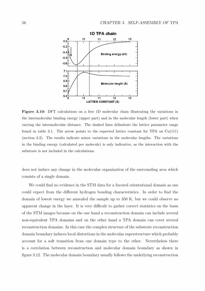
56 CHAPTER 3. SELF-ASSEMBLY OF TPA
Figure 3.10: DFT calculations on a free 1D molecular chain illustrating the variations in
the intermolecular binding energy (upper part) and in the molecular length (lower part) when
varying the intermolecular distance. The dashed lines delimitate the lattice parameter range
found in table 3.1. The arrow points to the expected lattice constant for TPA on Cu(111)
(section 3.2). The results indicate minor variations in the molecular lengths. The variations
in the binding energy (calculated per molecule) is only indicative, as the interaction with the
substrate is not included in the calculations.
does not induce any change in the molecular organization of the surrounding area which
consists of a single domain.
We could find no evidence in the STM data for a favored orientational domain as one
could expect from the different hydrogen bonding characteristics. In order to find the
domain of lowest energy we annealed the sample up to 350 K, but we could observe no
apparent change in the layer. It is very difficult to gather correct statistics on the basis
of the STM images because on the one hand a reconstruction domain can include several
non-equivalent TPA domains and on the other hand a TPA domain can cover several
reconstruction domains. In this case the complex structure of the substrate reconstruction
domain boundary induces local distortions in the molecular superstructure which probably
account for a soft transition from one domain type to the other. Nevertheless there
is a correlation between reconstruction and molecular domain boundary as shown in
figure 3.12. The molecular domain boundary usually follows the underlying reconstruction
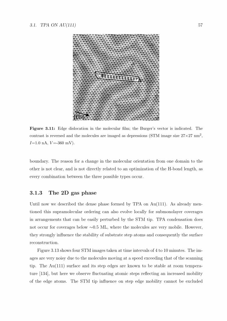
3.1. TPA ON AU(111) 57
Figure 3.11: Edge dislocation in the molecular film; the Burger’s vector is indicated. The
contrast is reversed and the molecules are imaged as depressions (STM image size 27×27 nm2,
I=1.0 nA, V =-360 mV).
boundary. The reason for a change in the molecular orientation from one domain to the
other is not clear, and is not directly related to an optimization of the H-bond length, as
every combination between the three possible types occur.
3.1.3 The 2D gas phase
Until now we described the dense phase formed by TPA on Au(111). As already men-
tioned this supramolecular ordering can also evolve locally for submonolayer coverages
in arrangements that can be easily perturbed by the STM tip. TPA condensation does
not occur for coverages below ∼0.5 ML, where the molecules are very mobile. However,
they strongly influence the stability of substrate step atoms and consequently the surface
reconstruction.
Figure 3.13 shows four STM images taken at time intervals of 4 to 10 minutes. The im-
ages are very noisy due to the molecules moving at a speed exceeding that of the scanning
tip. The Au(111) surface and its step edges are known to be stable at room tempera-
ture [134], but here we observe fluctuating atomic steps reflecting an increased mobility
of the edge atoms. The STM tip influence on step edge mobility cannot be excluded
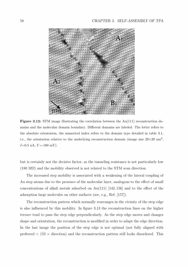
58 CHAPTER 3. SELF-ASSEMBLY OF TPA
Figure 3.12: STM image illustrating the correlation between the Au(111) reconstruction do-
mains and the molecular domain boundary. Different domains are labeled. The letter refers to
the absolute orientation, the numerical index refers to the domain type detailed in table 3.1,
i.e., the orientation relative to the underlying reconstruction domain (image size 29×29 nm2,
I=0.5 nA, V =-180 mV).
but is certainly not the decisive factor, as the tunneling resistance is not particularly low
(180 MΩ) and the mobility observed is not related to the STM scan direction.
The increased step mobility is associated with a weakening of the lateral coupling of
Au step atoms due to the presence of the molecular layer, analogous to the effect of small
concentrations of alkali metals adsorbed on Au(111) [142, 156] and to the effect of the
adsorption large molecules on other surfaces (see, e.g., Ref. [157]).
The reconstruction pattern which normally rearranges in the vicinity of the step edge
is also influenced by this mobility. In figure 3.13 the reconstruction lines on the higher
terrace tend to pass the step edge perpendicularly. As the step edge moves and changes
shape and orientation, the reconstruction is modified in order to adapt the edge direction.
In the last image the position of the step edge is not optimal (not fully aligned with
preferred < 110 > direction) and the reconstruction pattern still looks disordered. This
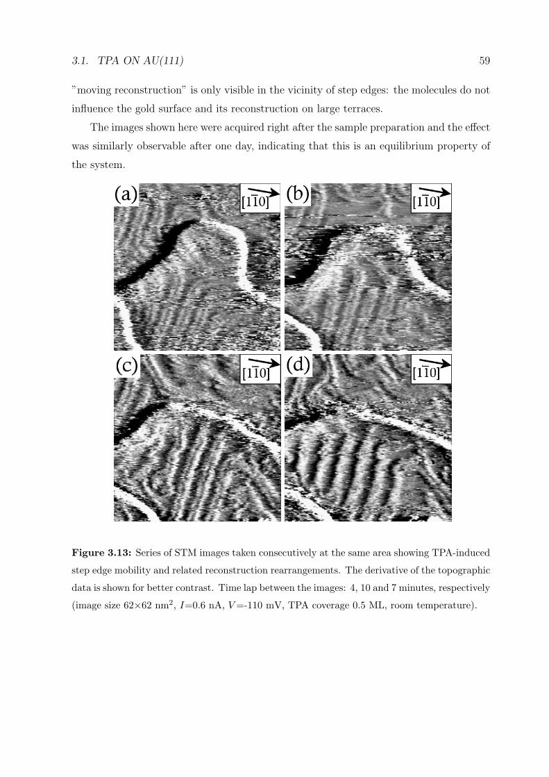
3.1. TPA ON AU(111) 59
”moving reconstruction” is only visible in the vicinity of step edges: the molecules do not
influence the gold surface and its reconstruction on large terraces.
The images shown here were acquired right after the sample preparation and the effect
was similarly observable after one day, indicating that this is an equilibrium property of
the system.
Figure 3.13: Series of STM images taken consecutively at the same area showing TPA-induced
step edge mobility and related reconstruction rearrangements. The derivative of the topographic
data is shown for better contrast. Time lap between the images: 4, 10 and 7 minutes, respectively
(image size 62×62 nm2, I=0.6 nA, V =-110 mV, TPA coverage 0.5 ML, room temperature).
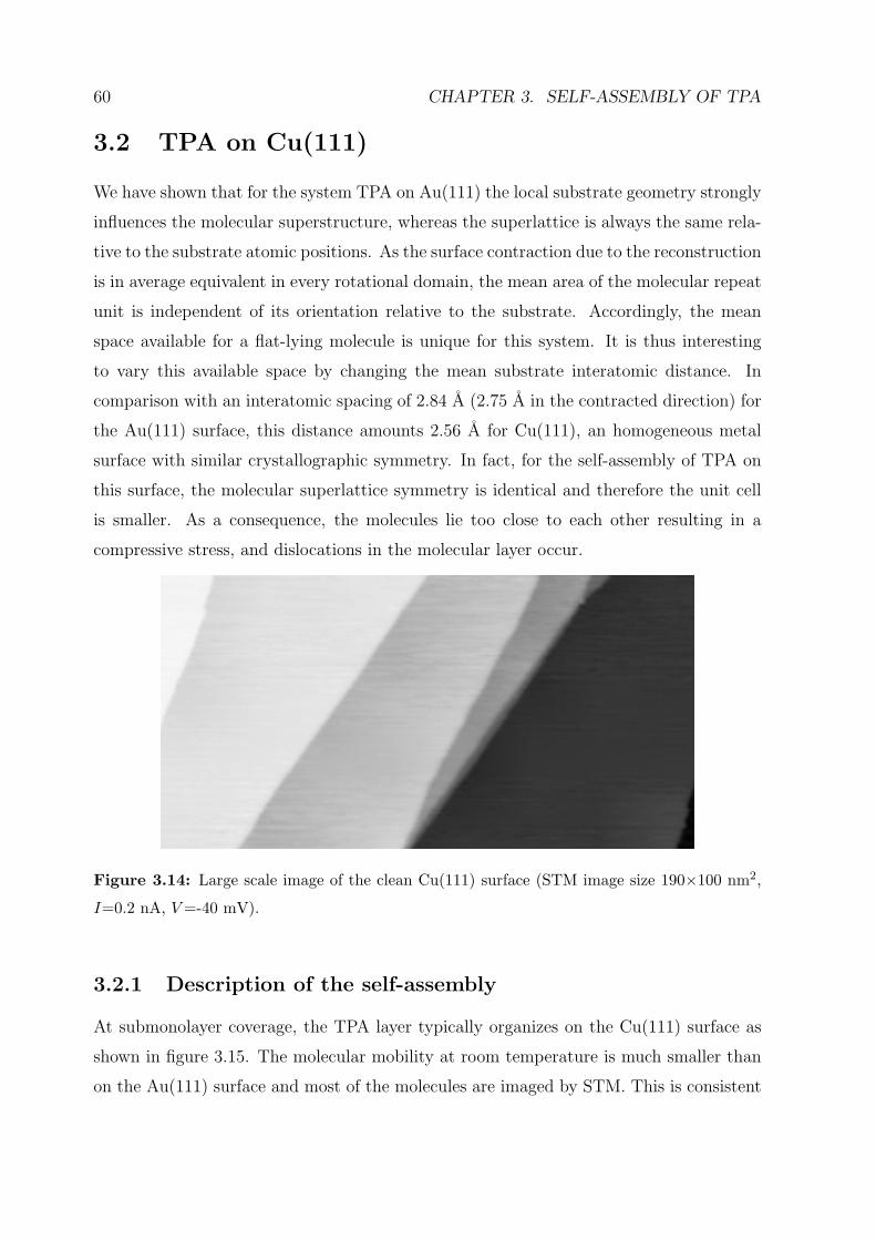
60 CHAPTER 3. SELF-ASSEMBLY OF TPA
3.2 TPA on Cu(111)
We have shown that for the system TPA on Au(111) the local substrate geometry strongly
influences the molecular superstructure, whereas the superlattice is always the same rela-
tive to the substrate atomic positions. As the surface contraction due to the reconstruction
is in average equivalent in every rotational domain, the mean area of the molecular repeat
unit is independent of its orientation relative to the substrate. Accordingly, the mean
space available for a flat-lying molecule is unique for this system. It is thus interesting
to vary this available space by changing the mean substrate interatomic distance. In
comparison with an interatomic spacing of 2.84 A (2.75 A in the contracted direction) for
the Au(111) surface, this distance amounts 2.56 A for Cu(111), an homogeneous metal
surface with similar crystallographic symmetry. In fact, for the self-assembly of TPA on
this surface, the molecular superlattice symmetry is identical and therefore the unit cell
is smaller. As a consequence, the molecules lie too close to each other resulting in a
compressive stress, and dislocations in the molecular layer occur.
Figure 3.14: Large scale image of the clean Cu(111) surface (STM image size 190×100 nm2,
I=0.2 nA, V =-40 mV).
3.2.1 Description of the self-assembly
At submonolayer coverage, the TPA layer typically organizes on the Cu(111) surface as
shown in figure 3.15. The molecular mobility at room temperature is much smaller than
on the Au(111) surface and most of the molecules are imaged by STM. This is consistent
3.2. TPA ON CU(111) 61
with the fact that Cu is more reactive than Au and with previous work on TPA on
Cu(100) [130, 158]. The molecules condense in large dense well-organized domains with
a quasi-hexagonal lattice symmetry. The layer is imaged at a mean height equal to the
bare substrate level, and the intralayer molecular corrugation is ∼1.1 A. Six different
orientations of the domains are observed.
The molecules are responsible for a faceting of the copper surface (as compared with
the typical morphology of clean Cu(111) as shown in figure 3.14). TPA interacts strongly
with the step edges which are therefore normally decorated by a double row of molecules.
The carboxyl group in the vicinity of a step edge is probably deprotonated to allow for the
formation of a strong metal-carboxylate bond. The induced charge transfer modifies the
electronic configuration of the molecule and the second carboxyl group is probably more
reactive for the formation of a hydrogen bond, and therefore always bond to a second
molecule [159].
Carboxylic acids frequently deprotonate upon deposition on a copper surface at room
temperature, leading even in some cases to an upright orientation of the molecules [135,
158,160,161]. On Cu(110), TPA molecules are deprotonated and lying flat at low coverage
or standing upright at higher coverage [135]. On Cu(100) the TPA are also deprotonated
but are lying flat at any coverage (submonolayer) [158]. The present observations suggest
that on Cu(111) the TPA molecules are lying flat and are not deprotonated in the do-
main phase. The oval shape of the molecules in the STM images, their longitudinal regular
alignment inside the domains and the intermolecular distances measured constitute co-
herent indications for the formation of flat-lying hydrogen-bonded linear motifs (Fig. 3.1).
Deprotonation occurs probably only for the carboxyl groups directly in contact with step
edges and not for the molecules on terraces. This statement is consistent with the fact
that a fcc(111) surface is more inert than the (100) orientation. However, this could
not be unambiguously demonstrated on the basis of the STM data, and further exper-
iments with X-ray Photoelectron Spectroscopy (XPS) and Near-Edge X-ray Absorption
Fine Structure (NEXAFS) techniques are in preparation for conclusive confirmation.
The substrate step edge directions do not reflect the threefold (111)-surface symmetry
but are parallel to one of the possible molecular lattice axes. It is thus the orientation of
the molecular ”domain” (which can be reduced to a seed of two rows) that determines the
step edge orientation through one of its high-symmetry directions. This is illustrated in
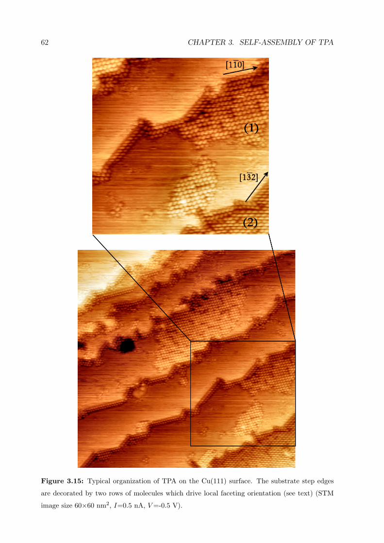
62 CHAPTER 3. SELF-ASSEMBLY OF TPA
Figure 3.15: Typical organization of TPA on the Cu(111) surface. The substrate step edges
are decorated by two rows of molecules which drive local faceting orientation (see text) (STM
image size 60×60 nm2, I=0.5 nA, V =-0.5 V).
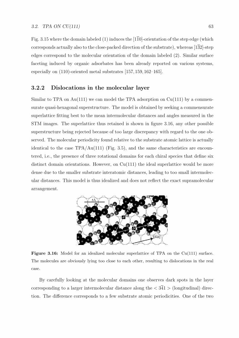
3.2. TPA ON CU(111) 63
Fig. 3.15 where the domain labeled (1) induces the [110]-orientation of the step edge (which
corresponds actually also to the close-packed direction of the substrate), whereas [132]-step
edges correspond to the molecular orientation of the domain labeled (2). Similar surface
faceting induced by organic adsorbates has been already reported on various systems,
especially on (110)-oriented metal substrates [157,159,162–165].
3.2.2 Dislocations in the molecular layer
Similar to TPA on Au(111) we can model the TPA adsorption on Cu(111) by a commen-
surate quasi-hexagonal superstructure. The model is obtained by seeking a commensurate
superlattice fitting best to the mean intermolecular distances and angles measured in the
STM images. The superlattice thus retained is shown in figure 3.16, any other possible
superstructure being rejected because of too large discrepancy with regard to the one ob-
served. The molecular periodicity found relative to the substrate atomic lattice is actually
identical to the case TPA/Au(111) (Fig. 3.5), and the same characteristics are encoun-
tered, i.e., the presence of three rotational domains for each chiral species that define six
distinct domain orientations. However, on Cu(111) the ideal superlattice would be more
dense due to the smaller substrate interatomic distances, leading to too small intermolec-
ular distances. This model is thus idealized and does not reflect the exact supramolecular
arrangement.
Figure 3.16: Model for an idealized molecular superlattice of TPA on the Cu(111) surface.
The molecules are obviously lying too close to each other, resulting to dislocations in the real
case.
By carefully looking at the molecular domains one observes dark spots in the layer
corresponding to a larger intermolecular distance along the < 341 > (longitudinal) direc-
tion. The difference corresponds to a few substrate atomic periodicities. One of the two
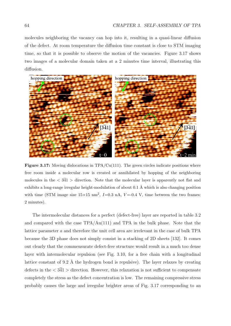
64 CHAPTER 3. SELF-ASSEMBLY OF TPA
molecules neighboring the vacancy can hop into it, resulting in a quasi-linear diffusion
of the defect. At room temperature the diffusion time constant is close to STM imaging
time, so that it is possible to observe the motion of the vacancies. Figure 3.17 shows
two images of a molecular domain taken at a 2 minutes time interval, illustrating this
diffusion.
Figure 3.17: Moving dislocations in TPA/Cu(111). The green circles indicate positions where
free room inside a molecular row is created or annihilated by hopping of the neighboring
molecules in the < 341 > direction. Note that the molecular layer is apparently not flat and
exhibits a long-range irregular height-modulation of about 0.1 A which is also changing position
with time (STM image size 15×15 nm2, I=0.3 nA, V =-0.4 V, time between the two frames:
2 minutes).
The intermolecular distances for a perfect (defect-free) layer are reported in table 3.2
and compared with the case TPA/Au(111) and TPA in the bulk phase. Note that the
lattice parameter a and therefore the unit cell area are irrelevant in the case of bulk TPA
because the 3D phase does not simply consist in a stacking of 2D sheets [132]. It comes
out clearly that the commensurate defect-free structure would result in a much too dense
layer with intermolecular repulsion (see Fig. 3.10, for a free chain with a longitudinal
lattice constant of 9.2 A the hydrogen bond is repulsive). The layer relaxes by creating
defects in the < 341 > direction. However, this relaxation is not sufficient to compensate
completely the stress as the defect concentration is low. The remaining compressive stress
probably causes the large and irregular brighter areas of Fig. 3.17 corresponding to an
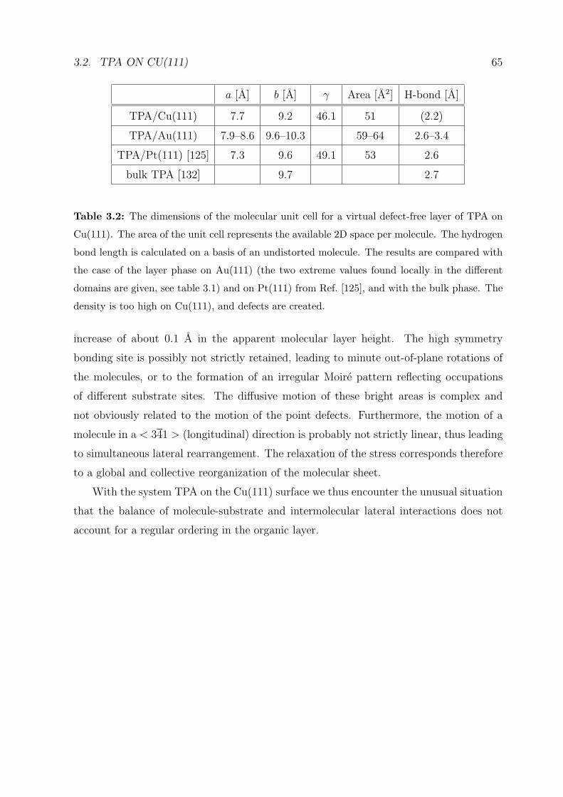
3.2. TPA ON CU(111) 65
a [A] b [A] γ Area [A2] H-bond [A]
TPA/Cu(111) 7.7 9.2 46.1 51 (2.2)
TPA/Au(111) 7.9–8.6 9.6–10.3 59–64 2.6–3.4
TPA/Pt(111) [125] 7.3 9.6 49.1 53 2.6
bulk TPA [132] 9.7 2.7
Table 3.2: The dimensions of the molecular unit cell for a virtual defect-free layer of TPA on
Cu(111). The area of the unit cell represents the available 2D space per molecule. The hydrogen
bond length is calculated on a basis of an undistorted molecule. The results are compared with
the case of the layer phase on Au(111) (the two extreme values found locally in the different
domains are given, see table 3.1) and on Pt(111) from Ref. [125], and with the bulk phase. The
density is too high on Cu(111), and defects are created.
increase of about 0.1 A in the apparent molecular layer height. The high symmetry
bonding site is possibly not strictly retained, leading to minute out-of-plane rotations of
the molecules, or to the formation of an irregular Moire pattern reflecting occupations
of different substrate sites. The diffusive motion of these bright areas is complex and
not obviously related to the motion of the point defects. Furthermore, the motion of a
molecule in a < 341 > (longitudinal) direction is probably not strictly linear, thus leading
to simultaneous lateral rearrangement. The relaxation of the stress corresponds therefore
to a global and collective reorganization of the molecular sheet.
With the system TPA on the Cu(111) surface we thus encounter the unusual situation
that the balance of molecule-substrate and intermolecular lateral interactions does not
account for a regular ordering in the organic layer.

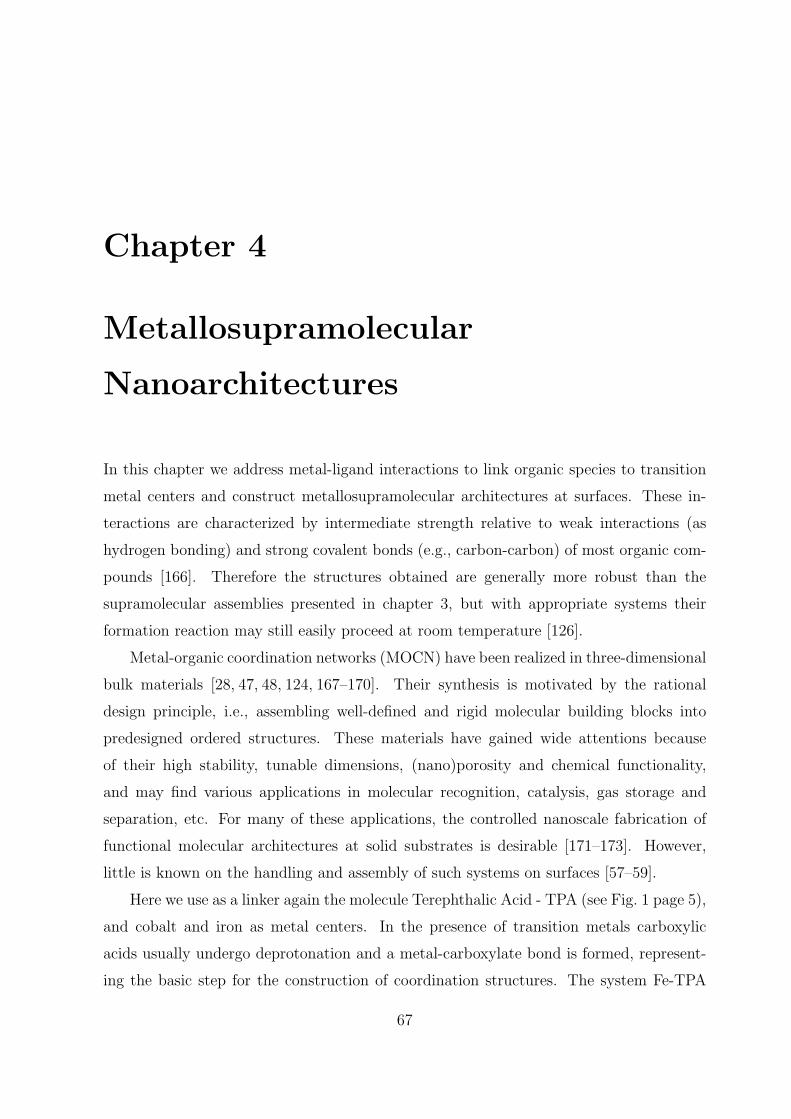
Chapter 4
Metallosupramolecular
Nanoarchitectures
In this chapter we address metal-ligand interactions to link organic species to transition
metal centers and construct metallosupramolecular architectures at surfaces. These in-
teractions are characterized by intermediate strength relative to weak interactions (as
hydrogen bonding) and strong covalent bonds (e.g., carbon-carbon) of most organic com-
pounds [166]. Therefore the structures obtained are generally more robust than the
supramolecular assemblies presented in chapter 3, but with appropriate systems their
formation reaction may still easily proceed at room temperature [126].
Metal-organic coordination networks (MOCN) have been realized in three-dimensional
bulk materials [28, 47, 48, 124, 167–170]. Their synthesis is motivated by the rational
design principle, i.e., assembling well-defined and rigid molecular building blocks into
predesigned ordered structures. These materials have gained wide attentions because
of their high stability, tunable dimensions, (nano)porosity and chemical functionality,
and may find various applications in molecular recognition, catalysis, gas storage and
separation, etc. For many of these applications, the controlled nanoscale fabrication of
functional molecular architectures at solid substrates is desirable [171–173]. However,
little is known on the handling and assembly of such systems on surfaces [57–59].
Here we use as a linker again the molecule Terephthalic Acid - TPA (see Fig. 1 page 5),
and cobalt and iron as metal centers. In the presence of transition metals carboxylic
acids usually undergo deprotonation and a metal-carboxylate bond is formed, represent-
ing the basic step for the construction of coordination structures. The system Fe-TPA
67
68 CHAPTER 4. METALLOSUPRAMOLECULAR NANOARCHITECTURES
has been extensively studied on the Cu(100) surface [130]. It organizes in various well-
ordered phases with square or rectangular unit cells, forming a variety of low-dimensional
arrangements including MOCN. Here the substrate used is Au(111). The peculiar sym-
metry of the compounds obtained does not match with the substrate symmetry, and their
ordering is consequently poor. On the other hand in situ observation of the dynamics
of Fe-TPA and Co-TPA network formation is possible. Furthermore, the use of Au(111)
is of interest because its surface reconstruction provides a regular mesoscopic patterning
which drives the large-scale organization of the metal-organic structures. Specific pat-
terns directly related to the inhomogeneities of the reconstructed Au(111) were already
obtained by molecular self-assembly by other groups [5, 7, 37], where the intermolecular
driving force consists of hydrogen bonding or weak interaction. We report micro- and
mesoscopic arrangements obtained by strong metal-ligand bonds, and where the influence
of the Au(111) chevron structure is straightforward.
In the following one monolayer (ML) refers to a complete monoatomic layer of Fe and
to half of a biatomic layer of Co on Au(111). For TPA, one monolayer refers to a complete
layer of the dense hydrogen-bonded phase.
Figure 4.1: a) Deposition of 0.07 ML of Fe on the Au(111) surface at room temperature.
The impurity atoms segregate at the elbow sites of the surface reconstruction pattern to form
a regular mesoscopic array of monolayer islands. (STM image size 100×80 nm2, I=1.3 nA,
V =20 mV). b) Large scale image of 0.14 ML of Co deposited on Au(111). The islands are
bilayered (STM image size 300×300 nm2, I=0.8 nA, V =-25 mV).
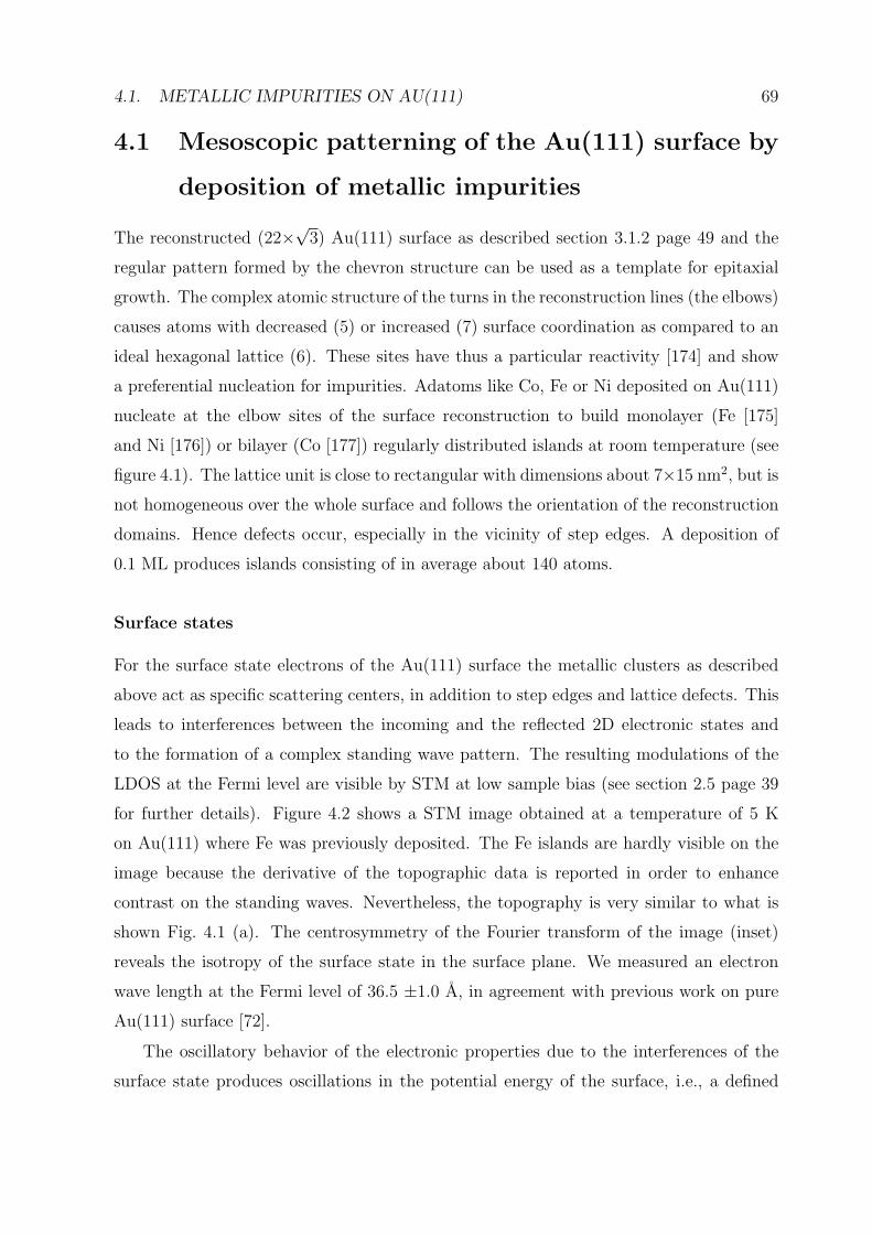
4.1. METALLIC IMPURITIES ON AU(111) 69
4.1 Mesoscopic patterning of the Au(111) surface by
deposition of metallic impurities
The reconstructed (22×√3) Au(111) surface as described section 3.1.2 page 49 and the
regular pattern formed by the chevron structure can be used as a template for epitaxial
growth. The complex atomic structure of the turns in the reconstruction lines (the elbows)
causes atoms with decreased (5) or increased (7) surface coordination as compared to an
ideal hexagonal lattice (6). These sites have thus a particular reactivity [174] and show
a preferential nucleation for impurities. Adatoms like Co, Fe or Ni deposited on Au(111)
nucleate at the elbow sites of the surface reconstruction to build monolayer (Fe [175]
and Ni [176]) or bilayer (Co [177]) regularly distributed islands at room temperature (see
figure 4.1). The lattice unit is close to rectangular with dimensions about 7×15 nm2, but is
not homogeneous over the whole surface and follows the orientation of the reconstruction
domains. Hence defects occur, especially in the vicinity of step edges. A deposition of
0.1 ML produces islands consisting of in average about 140 atoms.
Surface states
For the surface state electrons of the Au(111) surface the metallic clusters as described
above act as specific scattering centers, in addition to step edges and lattice defects. This
leads to interferences between the incoming and the reflected 2D electronic states and
to the formation of a complex standing wave pattern. The resulting modulations of the
LDOS at the Fermi level are visible by STM at low sample bias (see section 2.5 page 39
for further details). Figure 4.2 shows a STM image obtained at a temperature of 5 K
on Au(111) where Fe was previously deposited. The Fe islands are hardly visible on the
image because the derivative of the topographic data is reported in order to enhance
contrast on the standing waves. Nevertheless, the topography is very similar to what is
shown Fig. 4.1 (a). The centrosymmetry of the Fourier transform of the image (inset)
reveals the isotropy of the surface state in the surface plane. We measured an electron
wave length at the Fermi level of 36.5 ±1.0 A, in agreement with previous work on pure
Au(111) surface [72].
The oscillatory behavior of the electronic properties due to the interferences of the
surface state produces oscillations in the potential energy of the surface, i.e., a defined
70 CHAPTER 4. METALLOSUPRAMOLECULAR NANOARCHITECTURES
Figure 4.2: Standing waves on Au(111) in the presence of adsorbed Fe (same preparation
conditions as in Fig. 4.1 (a)). The interference pattern is caused by scattering of the surface
state electrons at step edges and at Fe islands located at the elbows sites of the reconstruction.
The derivative of the topographic data is shown for better contrast. Inset: the circle obtained
in the Fourier transform corresponds to the Fermi surface of the Shockley surface state, and the
dots to the surface reconstruction pattern (STM image size 100×100 nm2, I=0.4 nA, V =-10 mV,
T=5 K, Fe coverage 0.05 ML).
periodicity in potential wells, which mediates long-range interactions between adsor-
bates [178, 179]. In certain cases this can lead to the formation of well-ordered super-
lattices of adatoms at low temperature [180]. With the system Co or Fe on Au(111) these
interactions are much too weak in comparison with the modifications of the surface atom
reactivity due to the surface reconstruction. For a deposition at room temperature we did
not observe any correlation neither between the standing wave pattern and the metallic
cluster superstructure, nor with the molecular assembly described below.
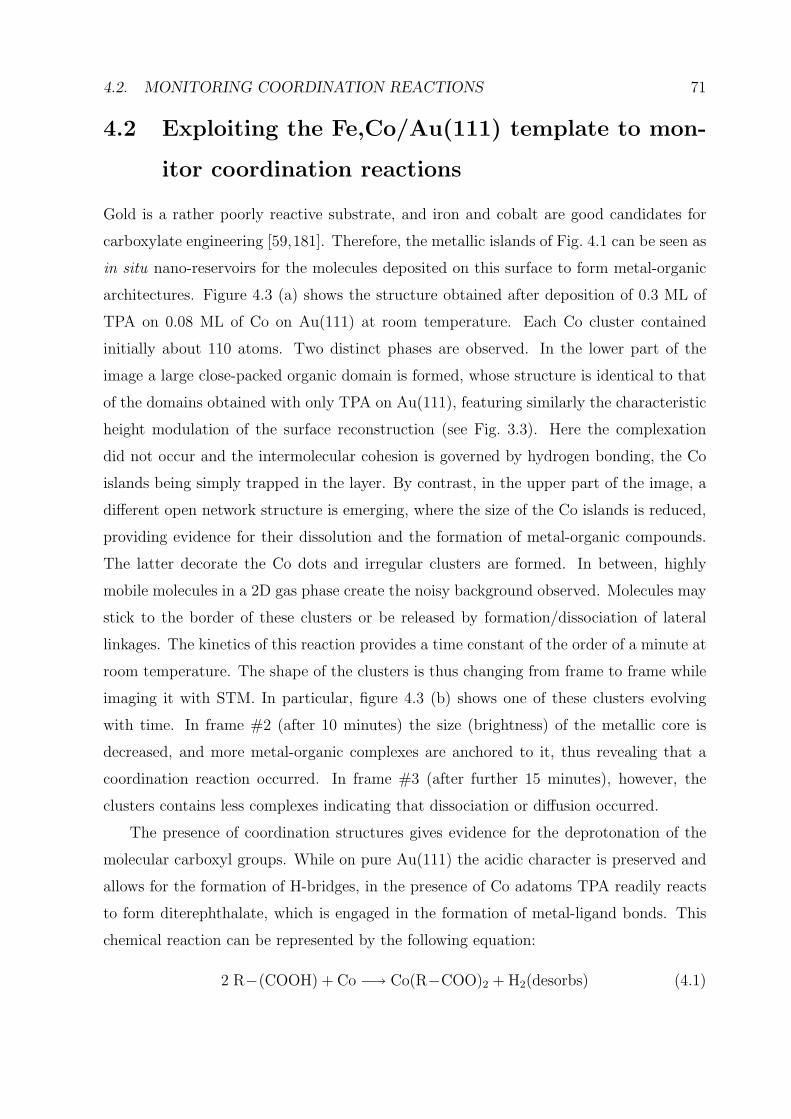
4.2. MONITORING COORDINATION REACTIONS 71
4.2 Exploiting the Fe,Co/Au(111) template to mon-
itor coordination reactions
Gold is a rather poorly reactive substrate, and iron and cobalt are good candidates for
carboxylate engineering [59,181]. Therefore, the metallic islands of Fig. 4.1 can be seen as
in situ nano-reservoirs for the molecules deposited on this surface to form metal-organic
architectures. Figure 4.3 (a) shows the structure obtained after deposition of 0.3 ML of
TPA on 0.08 ML of Co on Au(111) at room temperature. Each Co cluster contained
initially about 110 atoms. Two distinct phases are observed. In the lower part of the
image a large close-packed organic domain is formed, whose structure is identical to that
of the domains obtained with only TPA on Au(111), featuring similarly the characteristic
height modulation of the surface reconstruction (see Fig. 3.3). Here the complexation
did not occur and the intermolecular cohesion is governed by hydrogen bonding, the Co
islands being simply trapped in the layer. By contrast, in the upper part of the image, a
different open network structure is emerging, where the size of the Co islands is reduced,
providing evidence for their dissolution and the formation of metal-organic compounds.
The latter decorate the Co dots and irregular clusters are formed. In between, highly
mobile molecules in a 2D gas phase create the noisy background observed. Molecules may
stick to the border of these clusters or be released by formation/dissociation of lateral
linkages. The kinetics of this reaction provides a time constant of the order of a minute at
room temperature. The shape of the clusters is thus changing from frame to frame while
imaging it with STM. In particular, figure 4.3 (b) shows one of these clusters evolving
with time. In frame #2 (after 10 minutes) the size (brightness) of the metallic core is
decreased, and more metal-organic complexes are anchored to it, thus revealing that a
coordination reaction occurred. In frame #3 (after further 15 minutes), however, the
clusters contains less complexes indicating that dissociation or diffusion occurred.
The presence of coordination structures gives evidence for the deprotonation of the
molecular carboxyl groups. While on pure Au(111) the acidic character is preserved and
allows for the formation of H-bridges, in the presence of Co adatoms TPA readily reacts
to form diterephthalate, which is engaged in the formation of metal-ligand bonds. This
chemical reaction can be represented by the following equation:
2 R−(COOH) + Co −→ Co(R−COO)2 + H2(desorbs) (4.1)
72 CHAPTER 4. METALLOSUPRAMOLECULAR NANOARCHITECTURES
Atomic hydrogen is not stable on a noble metal surface at room temperature and recom-
bines into molecular hydrogen which desorbs [182]. The thermodynamical equilibrium
state of reaction (4.1) is therefore highly displaced to the right due to the disappearance
of one of its products. From the formal point of view of electron transfer, the desorbed
hydrogen molecule takes over the electrical charge which is necessary for the oxidation of
the metal center. After deprotonation of the carboxyl group
R−(COOH) −→ R−COO− + H+, (4.2)
the formal redox semi-equations can be represented as
2 H+ + 2 e− −→ H2(desorbs) (4.3)
and
Co −→ Co2+ + 2 e− (4.4)
The oxidation state CoII proposed is at this point only indicative. Its proper deter-
mination is the subject of the next chapter. Furthermore, depending on the structure
obtained the stoichiometry may vary, as it must be the case for the true 1D link presented
in section 4.3. The mechanism described above provides therefore a simple and general
picture which does not take into account the influence of the substrate. The latter may
be significant, in particular concerning charge transfer and the participation of formally
charged species (terephthalate).
The nanoporous networks show a characteristic decoration at their borders where the
grid motif of the interior is not continued. This phenomenon is understood as follows:
formally negatively charged carboxylate is reactive for hydrogen bond formation with the
hydrogens of a benzene ring, thus leading to the peculiar perpendicular coupling between
two molecules as shown in figure 4.6. This particular bonding scheme is characteristic of
the dimensionality of the system, and is typically not observable in three dimensions. In
fact, each molecule involved in a metal-organic bond through only one of its carboxylate
group (i.e., a molecule at the rim of a cluster) forms such a hydrogen bridge with its second
carboxylate group, as indicated, e.g., on the location marked by the arrow in Fig. 4.5. As
a consequence, we can deduce that the deprotonation reaction is mediated by the presence
of Co, and takes place for both of the carboxyl groups, but does not necessarily lead to
the formation of a stable metal-ligand bond.
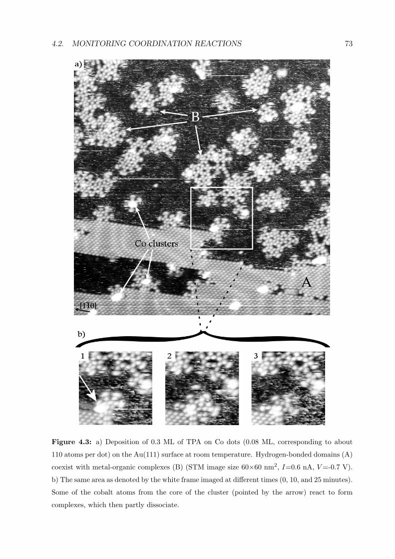
4.2. MONITORING COORDINATION REACTIONS 73
Figure 4.3: a) Deposition of 0.3 ML of TPA on Co dots (0.08 ML, corresponding to about
110 atoms per dot) on the Au(111) surface at room temperature. Hydrogen-bonded domains (A)
coexist with metal-organic complexes (B) (STM image size 60×60 nm2, I=0.6 nA, V =-0.7 V).
b) The same area as denoted by the white frame imaged at different times (0, 10, and 25 minutes).
Some of the cobalt atoms from the core of the cluster (pointed by the arrow) react to form
complexes, which then partly dissociate.
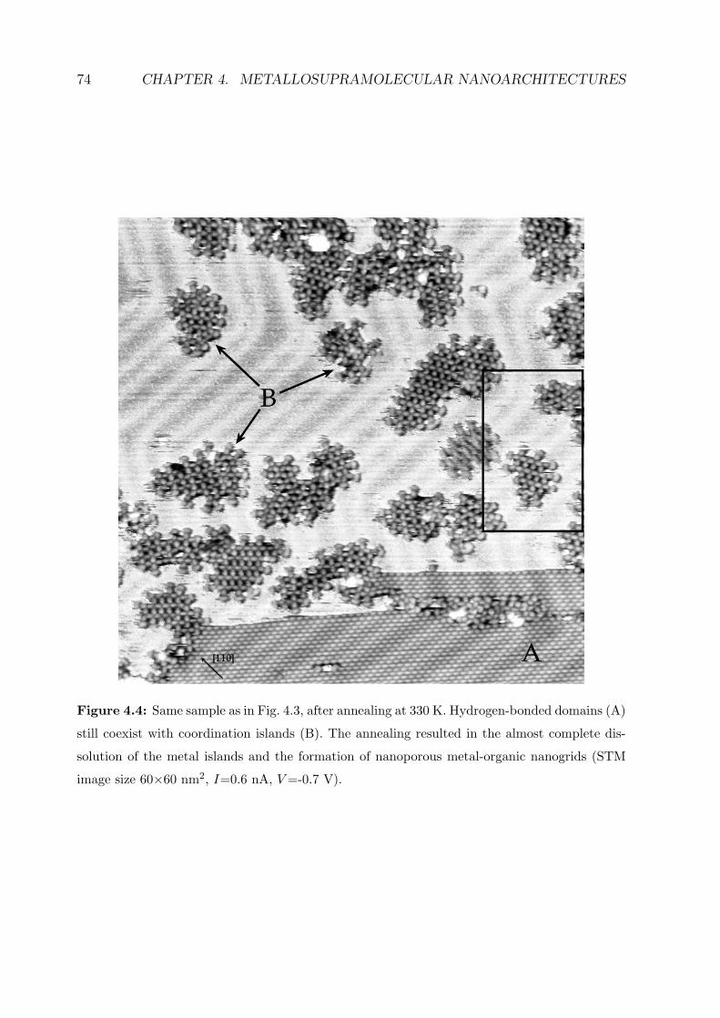
74 CHAPTER 4. METALLOSUPRAMOLECULAR NANOARCHITECTURES
Figure 4.4: Same sample as in Fig. 4.3, after annealing at 330 K. Hydrogen-bonded domains (A)
still coexist with coordination islands (B). The annealing resulted in the almost complete dis-
solution of the metal islands and the formation of nanoporous metal-organic nanogrids (STM
image size 60×60 nm2, I=0.6 nA, V =-0.7 V).
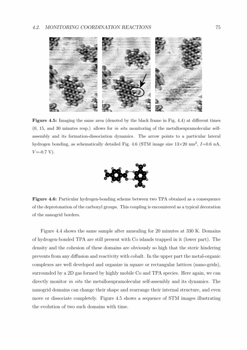
4.2. MONITORING COORDINATION REACTIONS 75
Figure 4.5: Imaging the same area (denoted by the black frame in Fig. 4.4) at different times
(0, 15, and 30 minutes resp.) allows for in situ monitoring of the metallosupramolecular self-
assembly and its formation-dissociation dynamics. The arrow points to a particular lateral
hydrogen bonding, as schematically detailed Fig. 4.6 (STM image size 13×20 nm2, I=0.6 nA,
V =-0.7 V).
Figure 4.6: Particular hydrogen-bonding scheme between two TPA obtained as a consequence
of the deprotonation of the carboxyl groups. This coupling is encountered as a typical decoration
of the nanogrid borders.
Figure 4.4 shows the same sample after annealing for 20 minutes at 330 K. Domains
of hydrogen-bonded TPA are still present with Co islands trapped in it (lower part). The
density and the cohesion of these domains are obviously so high that the steric hindering
prevents from any diffusion and reactivity with cobalt. In the upper part the metal-organic
complexes are well developed and organize in square or rectangular lattices (nano-grids),
surrounded by a 2D gas formed by highly mobile Co and TPA species. Here again, we can
directly monitor in situ the metallosupramolecular self-assembly and its dynamics. The
nanogrid domains can change their shape and rearrange their internal structure, and even
move or dissociate completely. Figure 4.5 shows a sequence of STM images illustrating
the evolution of two such domains with time.
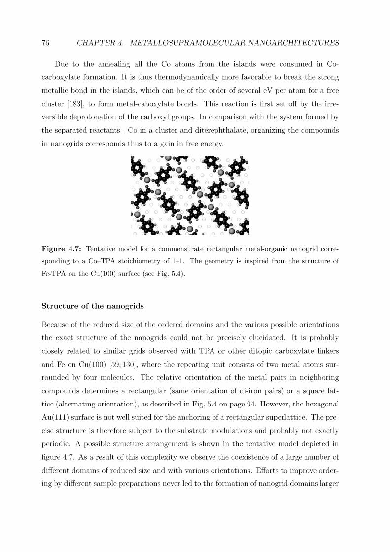
76 CHAPTER 4. METALLOSUPRAMOLECULAR NANOARCHITECTURES
Due to the annealing all the Co atoms from the islands were consumed in Co-
carboxylate formation. It is thus thermodynamically more favorable to break the strong
metallic bond in the islands, which can be of the order of several eV per atom for a free
cluster [183], to form metal-caboxylate bonds. This reaction is first set off by the irre-
versible deprotonation of the carboxyl groups. In comparison with the system formed by
the separated reactants - Co in a cluster and diterephthalate, organizing the compounds
in nanogrids corresponds thus to a gain in free energy.
Figure 4.7: Tentative model for a commensurate rectangular metal-organic nanogrid corre-
sponding to a Co–TPA stoichiometry of 1–1. The geometry is inspired from the structure of
Fe-TPA on the Cu(100) surface (see Fig. 5.4).
Structure of the nanogrids
Because of the reduced size of the ordered domains and the various possible orientations
the exact structure of the nanogrids could not be precisely elucidated. It is probably
closely related to similar grids observed with TPA or other ditopic carboxylate linkers
and Fe on Cu(100) [59, 130], where the repeating unit consists of two metal atoms sur-
rounded by four molecules. The relative orientation of the metal pairs in neighboring
compounds determines a rectangular (same orientation of di-iron pairs) or a square lat-
tice (alternating orientation), as described in Fig. 5.4 on page 94. However, the hexagonal
Au(111) surface is not well suited for the anchoring of a rectangular superlattice. The pre-
cise structure is therefore subject to the substrate modulations and probably not exactly
periodic. A possible structure arrangement is shown in the tentative model depicted in
figure 4.7. As a result of this complexity we observe the coexistence of a large number of
different domains of reduced size and with various orientations. Efforts to improve order-
ing by different sample preparations never led to the formation of nanogrid domains larger
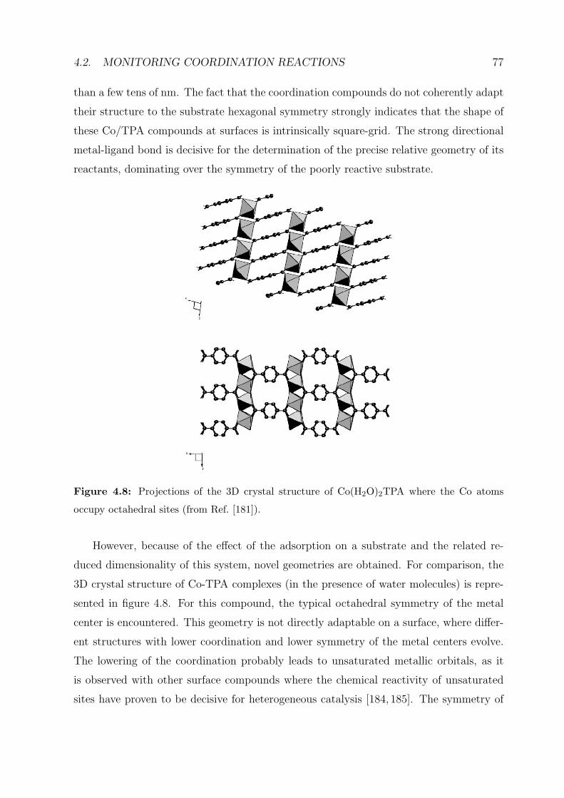
4.2. MONITORING COORDINATION REACTIONS 77
than a few tens of nm. The fact that the coordination compounds do not coherently adapt
their structure to the substrate hexagonal symmetry strongly indicates that the shape of
these Co/TPA compounds at surfaces is intrinsically square-grid. The strong directional
metal-ligand bond is decisive for the determination of the precise relative geometry of its
reactants, dominating over the symmetry of the poorly reactive substrate.
Figure 4.8: Projections of the 3D crystal structure of Co(H2O)2TPA where the Co atoms
occupy octahedral sites (from Ref. [181]).
However, because of the effect of the adsorption on a substrate and the related re-
duced dimensionality of this system, novel geometries are obtained. For comparison, the
3D crystal structure of Co-TPA complexes (in the presence of water molecules) is repre-
sented in figure 4.8. For this compound, the typical octahedral symmetry of the metal
center is encountered. This geometry is not directly adaptable on a surface, where differ-
ent structures with lower coordination and lower symmetry of the metal centers evolve.
The lowering of the coordination probably leads to unsaturated metallic orbitals, as it
is observed with other surface compounds where the chemical reactivity of unsaturated
sites have proven to be decisive for heterogeneous catalysis [184, 185]. The symmetry of
78 CHAPTER 4. METALLOSUPRAMOLECULAR NANOARCHITECTURES
the metal centers in the nanogrids is square planar. For the one-dimensional structure
presented below the symmetry is even lower. Compared with a relaxed 3D bulk struc-
ture, the symmetry reduction determines a new crystal field geometry. Even if the latter
and its influence on the electronic orbital symmetry are not precisely known yet, a first
characterization is proposed in the next chapter.
In contrast to the case Fe/TPA on Cu(100) [130], where the identification of the Fe
atom position is straightforward, no direct topographic evidence for the position of the
metal centers on Au(111) was found. The electronic structure and the precise geometry
of the total system needs to be investigated to understand this feature [84].
It is also interesting to note that on the Cu(100) surface no Co-TPA metal-organic
compounds evolve. The Fe-TPA system on this surface presents large homogeneous well-
ordered nanogrid structures. In comparison, the system Co or Fe and TPA on Au(111)
preserves its intrinsic square shape but is much more flexible and leads to the formation
of a large variety of nanoarchitectures.
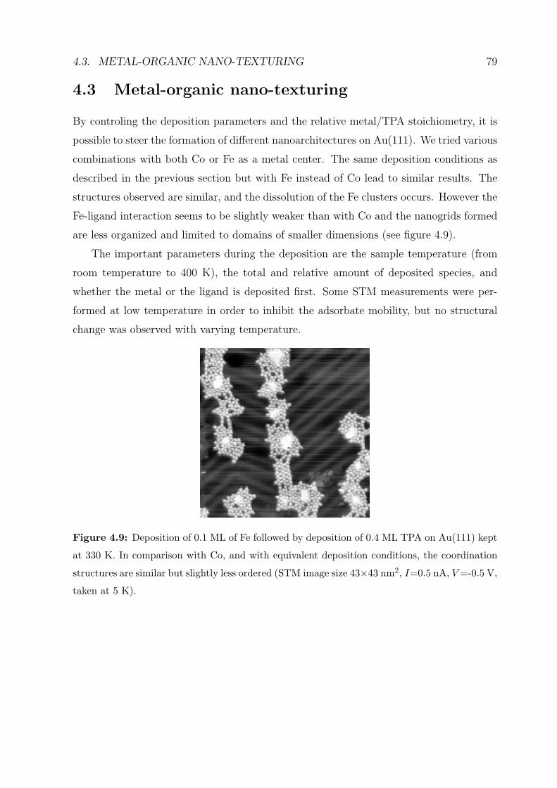
4.3. METAL-ORGANIC NANO-TEXTURING 79
4.3 Metal-organic nano-texturing
By controling the deposition parameters and the relative metal/TPA stoichiometry, it is
possible to steer the formation of different nanoarchitectures on Au(111). We tried various
combinations with both Co or Fe as a metal center. The same deposition conditions as
described in the previous section but with Fe instead of Co lead to similar results. The
structures observed are similar, and the dissolution of the Fe clusters occurs. However the
Fe-ligand interaction seems to be slightly weaker than with Co and the nanogrids formed
are less organized and limited to domains of smaller dimensions (see figure 4.9).
The important parameters during the deposition are the sample temperature (from
room temperature to 400 K), the total and relative amount of deposited species, and
whether the metal or the ligand is deposited first. Some STM measurements were per-
formed at low temperature in order to inhibit the adsorbate mobility, but no structural
change was observed with varying temperature.
Figure 4.9: Deposition of 0.1 ML of Fe followed by deposition of 0.4 ML TPA on Au(111) kept
at 330 K. In comparison with Co, and with equivalent deposition conditions, the coordination
structures are similar but slightly less ordered (STM image size 43×43 nm2, I=0.5 nA, V =-0.5 V,
taken at 5 K).
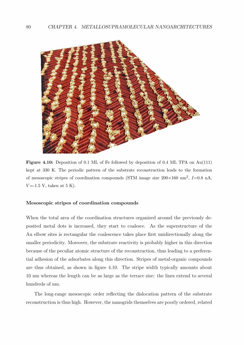
80 CHAPTER 4. METALLOSUPRAMOLECULAR NANOARCHITECTURES
Figure 4.10: Deposition of 0.1 ML of Fe followed by deposition of 0.4 ML TPA on Au(111)
kept at 330 K. The periodic pattern of the substrate reconstruction leads to the formation
of mesoscopic stripes of coordination compounds (STM image size 200×160 nm2, I=0.8 nA,
V =-1.5 V, taken at 5 K).
Mesoscopic stripes of coordination compounds
When the total area of the coordination structures organized around the previously de-
posited metal dots is increased, they start to coalesce. As the superstructure of the
Au elbow sites is rectangular the coalescence takes place first unidirectionally along the
smaller periodicity. Moreover, the substrate reactivity is probably higher in this direction
because of the peculiar atomic structure of the reconstruction, thus leading to a preferen-
tial adhesion of the adsorbates along this direction. Stripes of metal-organic compounds
are thus obtained, as shown in figure 4.10. The stripe width typically amounts about
10 nm whereas the length can be as large as the terrace size: the lines extend to several
hundreds of nm.
The long-range mesoscopic order reflecting the dislocation pattern of the substrate
reconstruction is thus high. However, the nanogrids themselves are poorly ordered, related
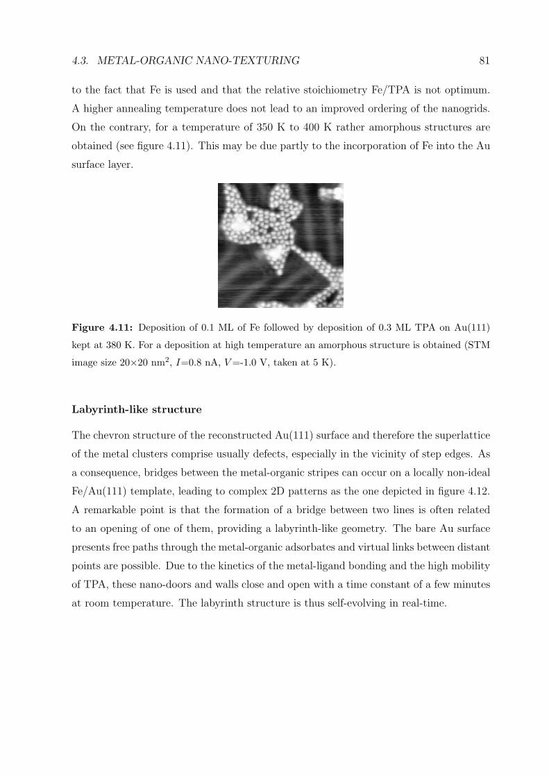
4.3. METAL-ORGANIC NANO-TEXTURING 81
to the fact that Fe is used and that the relative stoichiometry Fe/TPA is not optimum.
A higher annealing temperature does not lead to an improved ordering of the nanogrids.
On the contrary, for a temperature of 350 K to 400 K rather amorphous structures are
obtained (see figure 4.11). This may be due partly to the incorporation of Fe into the Au
surface layer.
Figure 4.11: Deposition of 0.1 ML of Fe followed by deposition of 0.3 ML TPA on Au(111)
kept at 380 K. For a deposition at high temperature an amorphous structure is obtained (STM
image size 20×20 nm2, I=0.8 nA, V =-1.0 V, taken at 5 K).
Labyrinth-like structure
The chevron structure of the reconstructed Au(111) surface and therefore the superlattice
of the metal clusters comprise usually defects, especially in the vicinity of step edges. As
a consequence, bridges between the metal-organic stripes can occur on a locally non-ideal
Fe/Au(111) template, leading to complex 2D patterns as the one depicted in figure 4.12.
A remarkable point is that the formation of a bridge between two lines is often related
to an opening of one of them, providing a labyrinth-like geometry. The bare Au surface
presents free paths through the metal-organic adsorbates and virtual links between distant
points are possible. Due to the kinetics of the metal-ligand bonding and the high mobility
of TPA, these nano-doors and walls close and open with a time constant of a few minutes
at room temperature. The labyrinth structure is thus self-evolving in real-time.
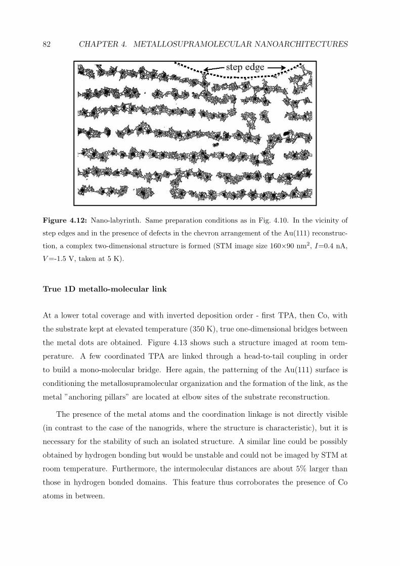
82 CHAPTER 4. METALLOSUPRAMOLECULAR NANOARCHITECTURES
Figure 4.12: Nano-labyrinth. Same preparation conditions as in Fig. 4.10. In the vicinity of
step edges and in the presence of defects in the chevron arrangement of the Au(111) reconstruc-
tion, a complex two-dimensional structure is formed (STM image size 160×90 nm2, I=0.4 nA,
V =-1.5 V, taken at 5 K).
True 1D metallo-molecular link
At a lower total coverage and with inverted deposition order - first TPA, then Co, with
the substrate kept at elevated temperature (350 K), true one-dimensional bridges between
the metal dots are obtained. Figure 4.13 shows such a structure imaged at room tem-
perature. A few coordinated TPA are linked through a head-to-tail coupling in order
to build a mono-molecular bridge. Here again, the patterning of the Au(111) surface is
conditioning the metallosupramolecular organization and the formation of the link, as the
metal ”anchoring pillars” are located at elbow sites of the substrate reconstruction.
The presence of the metal atoms and the coordination linkage is not directly visible
(in contrast to the case of the nanogrids, where the structure is characteristic), but it is
necessary for the stability of such an isolated structure. A similar line could be possibly
obtained by hydrogen bonding but would be unstable and could not be imaged by STM at
room temperature. Furthermore, the intermolecular distances are about 5% larger than
those in hydrogen bonded domains. This feature thus corroborates the presence of Co
atoms in between.
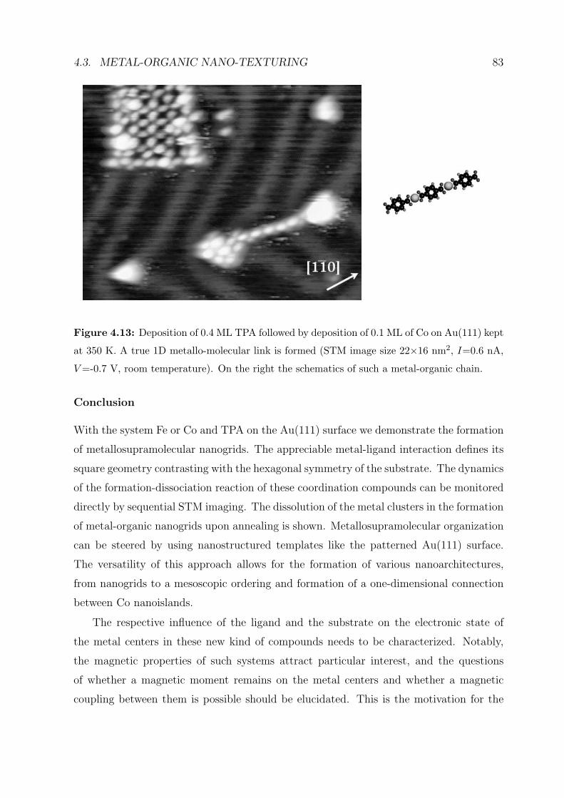
4.3. METAL-ORGANIC NANO-TEXTURING 83
Figure 4.13: Deposition of 0.4 ML TPA followed by deposition of 0.1 ML of Co on Au(111) kept
at 350 K. A true 1D metallo-molecular link is formed (STM image size 22×16 nm2, I=0.6 nA,
V =-0.7 V, room temperature). On the right the schematics of such a metal-organic chain.
Conclusion
With the system Fe or Co and TPA on the Au(111) surface we demonstrate the formation
of metallosupramolecular nanogrids. The appreciable metal-ligand interaction defines its
square geometry contrasting with the hexagonal symmetry of the substrate. The dynamics
of the formation-dissociation reaction of these coordination compounds can be monitored
directly by sequential STM imaging. The dissolution of the metal clusters in the formation
of metal-organic nanogrids upon annealing is shown. Metallosupramolecular organization
can be steered by using nanostructured templates like the patterned Au(111) surface.
The versatility of this approach allows for the formation of various nanoarchitectures,
from nanogrids to a mesoscopic ordering and formation of a one-dimensional connection
between Co nanoislands.
The respective influence of the ligand and the substrate on the electronic state of
the metal centers in these new kind of compounds needs to be characterized. Notably,
the magnetic properties of such systems attract particular interest, and the questions
of whether a magnetic moment remains on the metal centers and whether a magnetic
coupling between them is possible should be elucidated. This is the motivation for the

84 CHAPTER 4. METALLOSUPRAMOLECULAR NANOARCHITECTURES
studies presented in the next chapter. For future perspectives, the electronic properties of
the one-dimensional system presented should be investigated, e.g., by scanning tunneling
spectroscopy (STS), in particular to try to find out whether conduction along the line
and electron delocalization is obtained, as it is the case in similar 1D metallic systems
on surfaces [186,187]. Furthermore, the nanolabyrinth described above could be used for
percolation studies or investigations on the diffusivity of adsorbed species along random
2D paths [188].
Chapter 5
Electronic and Magnetic State of
Metal Centers in Surface-Supported
Coordination Architectures
As the dimensions of structures made of bulk magnetic material are drastically reduced
in size, the question of the magnetic order remaining at finite temperature is raised.
The elucidation of this problem has far reaching consequences both on the theoretical
understanding of magnetism and on magneto-recording technologies. Low dimensional
magnetic structures like colloids [189], 2D clusters [190], 1D nanowires [191] or even
single atoms on metal surfaces [192] exhibit very different properties compared with 3D
bulk materials, e.g., large magnetic moments and high magnetic anisotropy energy. In
such structures both the intrinsic magnetic properties and the type of magnetic order
depend critically on their size and geometry, as well as their composition. For atomic-scale
nanostructures on surfaces, a variety of geometrical arrangements can be obtained either
by patterning using self-assembly [180, 189–191, 193, 194], or by sequential manipulation
with STM [195, 196]. The advent of new techniques opens up new and exciting ways to
generate designed nanostructured materials that show novel functionalities. In particular,
crystal engineering of coordination polymers is of great interest because of novel topologies
of the compounds and the possibility of manipulating magnetic properties and electrical
conductivity [170,197,198].
The idea is then to combine coordination chemistry with a nanoscale approach. In con-
85
86 CHAPTER 5. ELECTRONIC STATE OF 2D METAL-ORGANIC COMPOUNDS
trast with previous attempts of organizing ex situ synthesized magnetic metal-containing
molecular entities at surfaces [57,199,200], the metal-organic structures presented in chap-
ter 4 demonstrate the great flexibility of the in situ approach for the fabrication of highly
ordered metallosupramolecular architectures. The micro- and mesoscopic shape, period-
icity and symmetry, as well as the ligand functionality are extensively tunable. In such
systems nevertheless, a series of important questions remains to be solved. First, the
electronic state of the metal center is modified by both the substrate interaction and the
coordination with the ligand, and needs to be investigated. Second, due to the periodicity
of the structures, a coupling between the magnetic centers may occur, mediated either by
the electronic states of the molecule or by the substrate electrons. In three-dimensional
coordination compounds the electronic properties of the metal centers has been widely
explored and characterized [170, 181, 197, 201–205]. There the metal-organic complexes
appear in the form of isolated ions, where the charge is usually balanced by the presence
of surrounding counterions. The oxidation state of the metal ion is thus related to its
coordination and to the global charge of the complex. At metal surfaces the situation
is different. The charge on both the metal and the ligand is strongly affected by the
presence of the electrons in the conduction band of the substrate, which effectively screen
any charged adsorbate. The complex should therefore not be considered as an ion but
rather as a neutral species partly hybridized with the substrate. Moreover, the planar
arrangement and symmetry, which are influencing to a large part the electronic state, are
usually not encountered in three dimensions. The determination of the oxidation state
of the central atom in surface-supported coordination compounds thus requires special
consideration in comparison with 3D compounds.
The magnetic and electronic states of the metal center in surface-supported coor-
dination structures have been investigated here for the first time by X-ray Absorption
Spectroscopy (XAS) and X-ray Magnetic Circular Dichroism (XMCD). Our findings show
that the electronic state is dominated by the coupling to the ligand rather than to the
substrate. This opens a great variety of options to effectively modify the valence state
and magnetic moment of transition metal centers at surfaces. By an appropriate choice
of the ligand, its functionality, and the resulting topographic structure [59, 130], it may
thus become possible to finely tune the electronic properties of the metal center. This is
similar to what is done in 3D coordination chemistry where the number of the various
5.1. XAS AND XMCD SPECTROSCOPY 87
combinations metal-ligand-structure is quasi infinite. Further experiments with different
substrates and molecular functionalities are planned to test this hypothesis.
5.1 XAS and XMCD Spectroscopy
General considerations
Synchrotron radiation in the soft X-ray range allows access to the strong dipole-permitted
(core 2p → valence 3d) excitations in transition-metal ferromagnets, and (core 3d, 4d →valence 4f) in rare-earth magnetic materials. For transition metals, L-edge XAS is highly
sensitive to the number and configuration of 3d electrons, hence to the spin state and
oxidation state [206,207]. Since the development of high-resolution synchrotron radiation
sources in the relevant energy range, it has successfully been used to study the electronic
structure and symmetry of coordination compounds [201,202,205] as well as biologically
relevant complexes [208–210].
X-ray absorption experiments with polarized light allow to extract a great deal of
information on the magnetic state of such systems. After the first practical demonstration
of X-ray magnetic dichroism (XMD) using linearly polarized light in 1986 [211], XMD with
the ”C”, i.e., using circularly polarized light, has been developed both experimentally [212]
and theoretically [213] into a powerful quantitative magnetometry tool. XMCD is element-
specific, has sub-monolayer sensitivity, and can be used to measure magnetization loops.
It allows to identify the moment orientation in ultrathin films of magnetic materials and,
unique among surface-sensitive magneto-optical techniques, to determine separately the
spin and orbital magnetic moments of a given element together with their anisotropies.
In order to achieve its high sensitivity, XMCD requires a tunable source of polarized light
in the UV - soft X-ray range and an extremely intense photon beam, which can only be
obtained in an advanced synchrotron radiation facility.
The emission of electrons resulting from light absorption is the base of the photoab-
sorption spectroscopy. In the photoelectric effect, an electron in a bound state of a solid
is excited into an unbound (free-electron) state by absorption of a photon of energy ω.
The excitation of primary and secondary electrons escaping the solid yields a measur-
able photocurrent. The electronic transitions involved are closely related to the electronic
structure of the sample and to the characteristics of the incident light. The corresponding
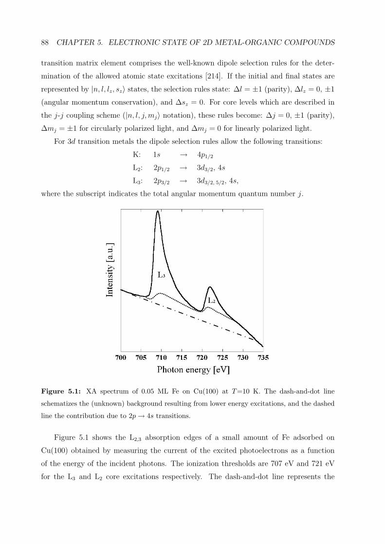
88 CHAPTER 5. ELECTRONIC STATE OF 2D METAL-ORGANIC COMPOUNDS
transition matrix element comprises the well-known dipole selection rules for the deter-
mination of the allowed atomic state excitations [214]. If the initial and final states are
represented by |n, l, lz, sz〉 states, the selection rules state: ∆l = ±1 (parity), ∆lz = 0, ±1
(angular momentum conservation), and ∆sz = 0. For core levels which are described in
the j-j coupling scheme (|n, l, j, mj〉 notation), these rules become: ∆j = 0, ±1 (parity),
∆mj = ±1 for circularly polarized light, and ∆mj = 0 for linearly polarized light.
For 3d transition metals the dipole selection rules allow the following transitions:
K: 1s → 4p1/2
L2: 2p1/2 → 3d3/2, 4s
L3: 2p3/2 → 3d3/2, 5/2, 4s,
where the subscript indicates the total angular momentum quantum number j.
Figure 5.1: XA spectrum of 0.05 ML Fe on Cu(100) at T=10 K. The dash-and-dot line
schematizes the (unknown) background resulting from lower energy excitations, and the dashed
line the contribution due to 2p → 4s transitions.
Figure 5.1 shows the L2,3 absorption edges of a small amount of Fe adsorbed on
Cu(100) obtained by measuring the current of the excited photoelectrons as a function
of the energy of the incident photons. The ionization thresholds are 707 eV and 721 eV
for the L3 and L2 core excitations respectively. The dash-and-dot line represents the
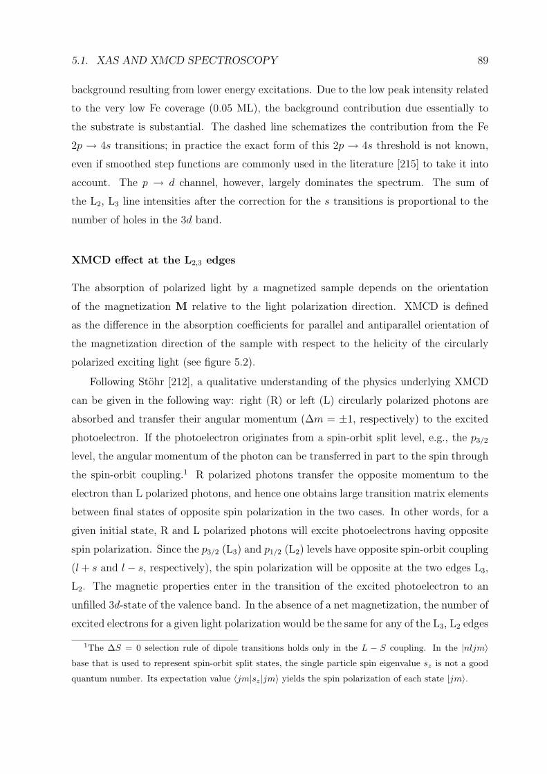
5.1. XAS AND XMCD SPECTROSCOPY 89
background resulting from lower energy excitations. Due to the low peak intensity related
to the very low Fe coverage (0.05 ML), the background contribution due essentially to
the substrate is substantial. The dashed line schematizes the contribution from the Fe
2p → 4s transitions; in practice the exact form of this 2p → 4s threshold is not known,
even if smoothed step functions are commonly used in the literature [215] to take it into
account. The p → d channel, however, largely dominates the spectrum. The sum of
the L2, L3 line intensities after the correction for the s transitions is proportional to the
number of holes in the 3d band.
XMCD effect at the L2,3 edges
The absorption of polarized light by a magnetized sample depends on the orientation
of the magnetization M relative to the light polarization direction. XMCD is defined
as the difference in the absorption coefficients for parallel and antiparallel orientation of
the magnetization direction of the sample with respect to the helicity of the circularly
polarized exciting light (see figure 5.2).
Following Stohr [212], a qualitative understanding of the physics underlying XMCD
can be given in the following way: right (R) or left (L) circularly polarized photons are
absorbed and transfer their angular momentum (∆m = ±1, respectively) to the excited
photoelectron. If the photoelectron originates from a spin-orbit split level, e.g., the p3/2
level, the angular momentum of the photon can be transferred in part to the spin through
the spin-orbit coupling.1 R polarized photons transfer the opposite momentum to the
electron than L polarized photons, and hence one obtains large transition matrix elements
between final states of opposite spin polarization in the two cases. In other words, for a
given initial state, R and L polarized photons will excite photoelectrons having opposite
spin polarization. Since the p3/2 (L3) and p1/2 (L2) levels have opposite spin-orbit coupling
(l + s and l − s, respectively), the spin polarization will be opposite at the two edges L3,
L2. The magnetic properties enter in the transition of the excited photoelectron to an
unfilled 3d-state of the valence band. In the absence of a net magnetization, the number of
excited electrons for a given light polarization would be the same for any of the L3, L2 edges
1The ∆S = 0 selection rule of dipole transitions holds only in the L − S coupling. In the |nljm〉base that is used to represent spin-orbit split states, the single particle spin eigenvalue sz is not a good
quantum number. Its expectation value 〈jm|sz|jm〉 yields the spin polarization of each state |jm〉.
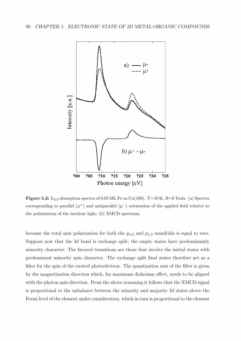
90 CHAPTER 5. ELECTRONIC STATE OF 2D METAL-ORGANIC COMPOUNDS
Figure 5.2: L2,3-absorption spectra of 0.05 ML Fe on Cu(100). T=10 K, B=6 Tesla. (a) Spectra
corresponding to parallel (µ+) and antiparallel (µ−) orientation of the applied field relative to
the polarization of the incident light; (b) XMCD spectrum.
because the total spin polarization for both the p3/2 and p1/2 manifolds is equal to zero.
Suppose now that the 3d band is exchange split; the empty states have predominantly
minority character. The favored transitions are those that involve the initial states with
predominant minority spin character. The exchange split final states therefore act as a
filter for the spin of the excited photoelectron. The quantization axis of the filter is given
by the magnetization direction which, for maximum dichroism effect, needs to be aligned
with the photon spin direction. From the above reasoning it follows that the XMCD signal
is proportional to the unbalance between the minority and majority 3d states above the
Fermi level of the element under consideration, which in turn is proportional to the element
5.1. XAS AND XMCD SPECTROSCOPY 91
magnetization. The maximum XMCD effect is obtained for a photon helicity parallel to
the sample magnetization, thereby allowing to probe its orientation.
XMCD sum rules
Two important magneto-optical sum rules [216–218] relate the XAS and XMCD data to
the element-specific orbital and spin magnetic moments. The sum rules have been tested
by band-structure calculations [219,220] and have been verified experimentally [215].
By noting µ+ and µ− the absorption coefficients for parallel and antiparallel orienta-
tion, respectively, of the sample magnetization relative to the incident light polarization,
and in the case of L3, L2 transitions, one calculates the d-shell angular momentum expec-
tation value 〈Lz〉 as
1
2nh
〈Lz〉 =
∫L3+L2
dE(µ+ − µ−)∫L3+L2
dE(µ+ + µ− + µ0), (5.1)
where nh is the number of holes in the d shell, and the denominator term is the normaliza-
tion to the unpolarized (isotropic) absorption spectrum (µ0 is the absorption coefficient
for linearly polarized light and is usually taken to be the average between µ+ and µ−).
z refers to the direction of the incident photon beam.
The second rule relates the XMCD signal to expectation values of the spin operator
Sz and of the intra-atomic magnetic dipole operator Tz [218]:
2
3nh
(〈Sz〉 +
7
2〈Tz〉
)=
∫L3
dE(µ+ − µ−) − 2∫
L2dE(µ+ − µ−)∫
L3+L2dE(µ+ + µ− + µ0)
. (5.2)
The term containing 〈Tz〉 arises from the multipole expansion of the spin density and
depends on the asymmetry of the atomic charge distribution.
The orbital and spin magnetic moments are related to the expectation values of the
Lz, Sz operators by
µL = −µB〈Lz〉 (5.3)
µS = −2µB〈Sz〉 . (5.4)
Some ambiguity remains in the integration limits, the background substraction and in
the value to take for nh when determining the absolute value of µL and µS. However the
ratio µL/µeffS (where µeff
S = −2µB〈Sz〉 − 7µB〈Tz〉) can be obtained in a straightforward
way.
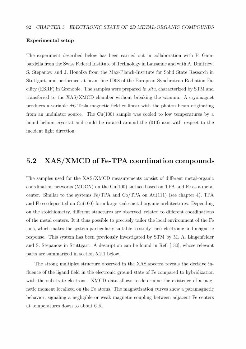
92 CHAPTER 5. ELECTRONIC STATE OF 2D METAL-ORGANIC COMPOUNDS
Experimental setup
The experiment described below has been carried out in collaboration with P. Gam-
bardella from the Swiss Federal Institute of Technology in Lausanne and with A. Dmitriev,
S. Stepanow and J. Honolka from the Max-Planck-Institute for Solid State Research in
Stuttgart, and performed at beam line ID08 of the European Synchrotron Radiation Fa-
cility (ESRF) in Grenoble. The samples were prepared in situ, characterized by STM and
transferred to the XAS/XMCD chamber without breaking the vacuum. A cryomagnet
produces a variable ±6 Tesla magnetic field collinear with the photon beam originating
from an undulator source. The Cu(100) sample was cooled to low temperatures by a
liquid helium cryostat and could be rotated around the (010) axis with respect to the
incident light direction.
5.2 XAS/XMCD of Fe-TPA coordination compounds
The samples used for the XAS/XMCD measurements consist of different metal-organic
coordination networks (MOCN) on the Cu(100) surface based on TPA and Fe as a metal
center. Similar to the systems Fe/TPA and Co/TPA on Au(111) (see chapter 4), TPA
and Fe co-deposited on Cu(100) form large-scale metal-organic architectures. Depending
on the stoichiometry, different structures are observed, related to different coordinations
of the metal centers. It it thus possible to precisely tailor the local environment of the Fe
ions, which makes the system particularly suitable to study their electronic and magnetic
response. This system has been previously investigated by STM by M. A. Lingenfelder
and S. Stepanow in Stuttgart. A description can be found in Ref. [130], whose relevant
parts are summarized in section 5.2.1 below.
The strong multiplet structure observed in the XAS spectra reveals the decisive in-
fluence of the ligand field in the electronic ground state of Fe compared to hybridization
with the substrate electrons. XMCD data allows to determine the existence of a mag-
netic moment localized on the Fe atoms. The magnetization curves show a paramagnetic
behavior, signaling a negligible or weak magnetic coupling between adjacent Fe centers
at temperatures down to about 6 K.
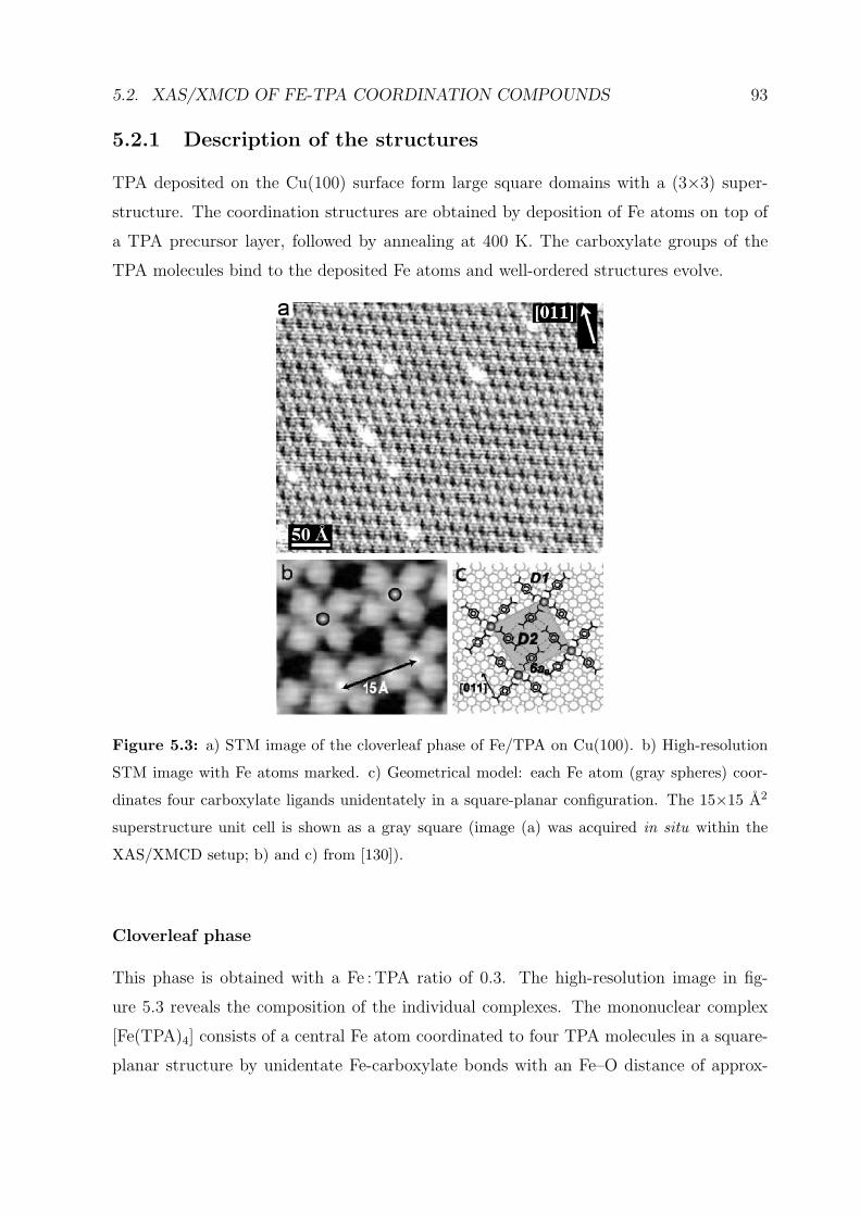
5.2. XAS/XMCD OF FE-TPA COORDINATION COMPOUNDS 93
5.2.1 Description of the structures
TPA deposited on the Cu(100) surface form large square domains with a (3×3) super-
structure. The coordination structures are obtained by deposition of Fe atoms on top of
a TPA precursor layer, followed by annealing at 400 K. The carboxylate groups of the
TPA molecules bind to the deposited Fe atoms and well-ordered structures evolve.
Figure 5.3: a) STM image of the cloverleaf phase of Fe/TPA on Cu(100). b) High-resolution
STM image with Fe atoms marked. c) Geometrical model: each Fe atom (gray spheres) coor-
dinates four carboxylate ligands unidentately in a square-planar configuration. The 15×15 A2
superstructure unit cell is shown as a gray square (image (a) was acquired in situ within the
XAS/XMCD setup; b) and c) from [130]).
Cloverleaf phase
This phase is obtained with a Fe : TPA ratio of 0.3. The high-resolution image in fig-
ure 5.3 reveals the composition of the individual complexes. The mononuclear complex
[Fe(TPA)4] consists of a central Fe atom coordinated to four TPA molecules in a square-
planar structure by unidentate Fe-carboxylate bonds with an Fe–O distance of approx-
94 CHAPTER 5. ELECTRONIC STATE OF 2D METAL-ORGANIC COMPOUNDS
imately 2 A. In view of the fact that the carboxylate group is a strong hydrogen bond
acceptor, the [Fe(TPA)4] arrangement may be further stabilized by intracomplex C–H· · ·Ohydrogen bonding. The complexes are organized in a (6×6) unit cell with respect to the
substrate and form a well-ordered array covering all the terraces of the substrate. A close
inspection of the high-resolution image and model reveals that a given TPA molecule
in the [Fe(TPA)4] complex coordinates to the central Fe atom through the ”left-hand”
oxygen atom of the carboxylate moiety. [Fe(TPA)4] complexes with ”right-hand” oxy-
gen coordination are similarly encountered in others domains, which leads to a distinct
clockwise or anticlockwise chirality of the complexes.
Figure 5.4: a) STM image of the 2D reticulated single-row phase of Fe/TPA on Cu(100),
where four TPA are linked to two Fe atoms. High-resolution STM images reveal the geometrical
arrangements in the α (upper inset) and β (bottom inset) phases, which differ in the orientation
of the neighboring iron pairs. b) and c) Geometrical models depicting atomic and molecular
positioning in the two isomeric structures and the corresponding unit cells (from [130]).
Single-row phase
This phase is obtained with a Fe : TPA ratio of 1.2. Here Fe pairs with an Fe–Fe spacing
of 5 A (2 times the substrate atomic periodicity a0) are linked to four TPA molecules
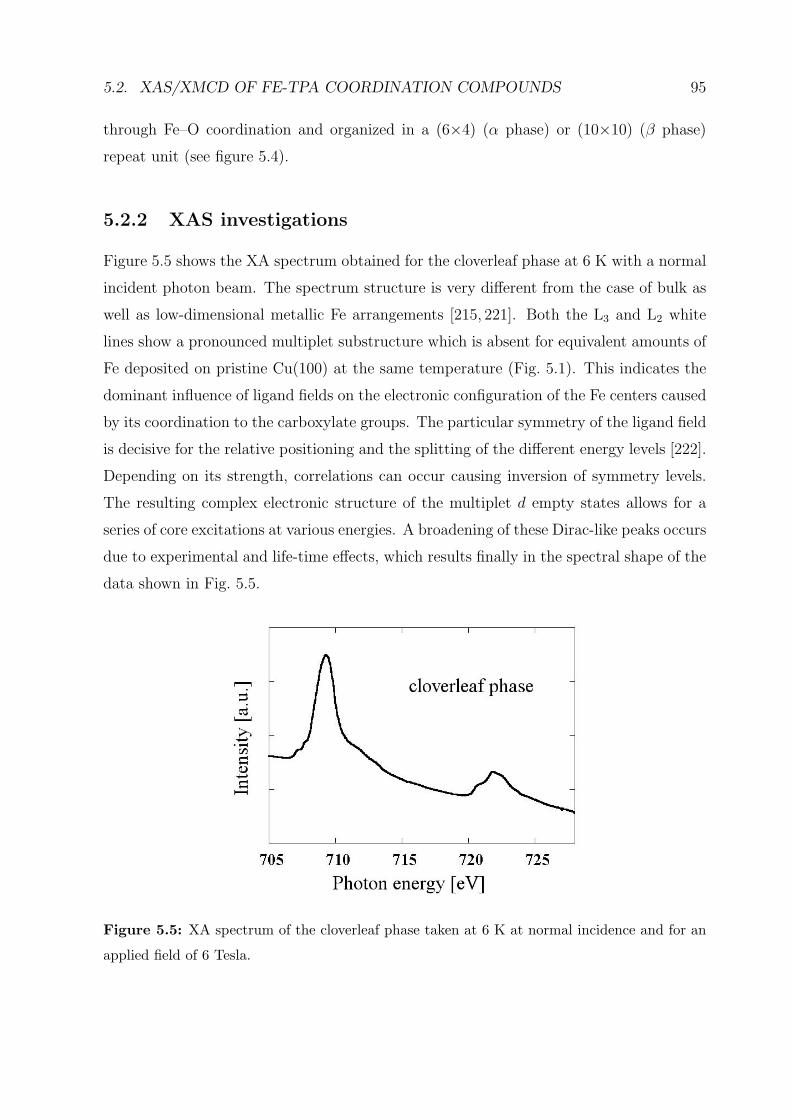
5.2. XAS/XMCD OF FE-TPA COORDINATION COMPOUNDS 95
through Fe–O coordination and organized in a (6×4) (α phase) or (10×10) (β phase)
repeat unit (see figure 5.4).
5.2.2 XAS investigations
Figure 5.5 shows the XA spectrum obtained for the cloverleaf phase at 6 K with a normal
incident photon beam. The spectrum structure is very different from the case of bulk as
well as low-dimensional metallic Fe arrangements [215, 221]. Both the L3 and L2 white
lines show a pronounced multiplet substructure which is absent for equivalent amounts of
Fe deposited on pristine Cu(100) at the same temperature (Fig. 5.1). This indicates the
dominant influence of ligand fields on the electronic configuration of the Fe centers caused
by its coordination to the carboxylate groups. The particular symmetry of the ligand field
is decisive for the relative positioning and the splitting of the different energy levels [222].
Depending on its strength, correlations can occur causing inversion of symmetry levels.
The resulting complex electronic structure of the multiplet d empty states allows for a
series of core excitations at various energies. A broadening of these Dirac-like peaks occurs
due to experimental and life-time effects, which results finally in the spectral shape of the
data shown in Fig. 5.5.
Figure 5.5: XA spectrum of the cloverleaf phase taken at 6 K at normal incidence and for an
applied field of 6 Tesla.
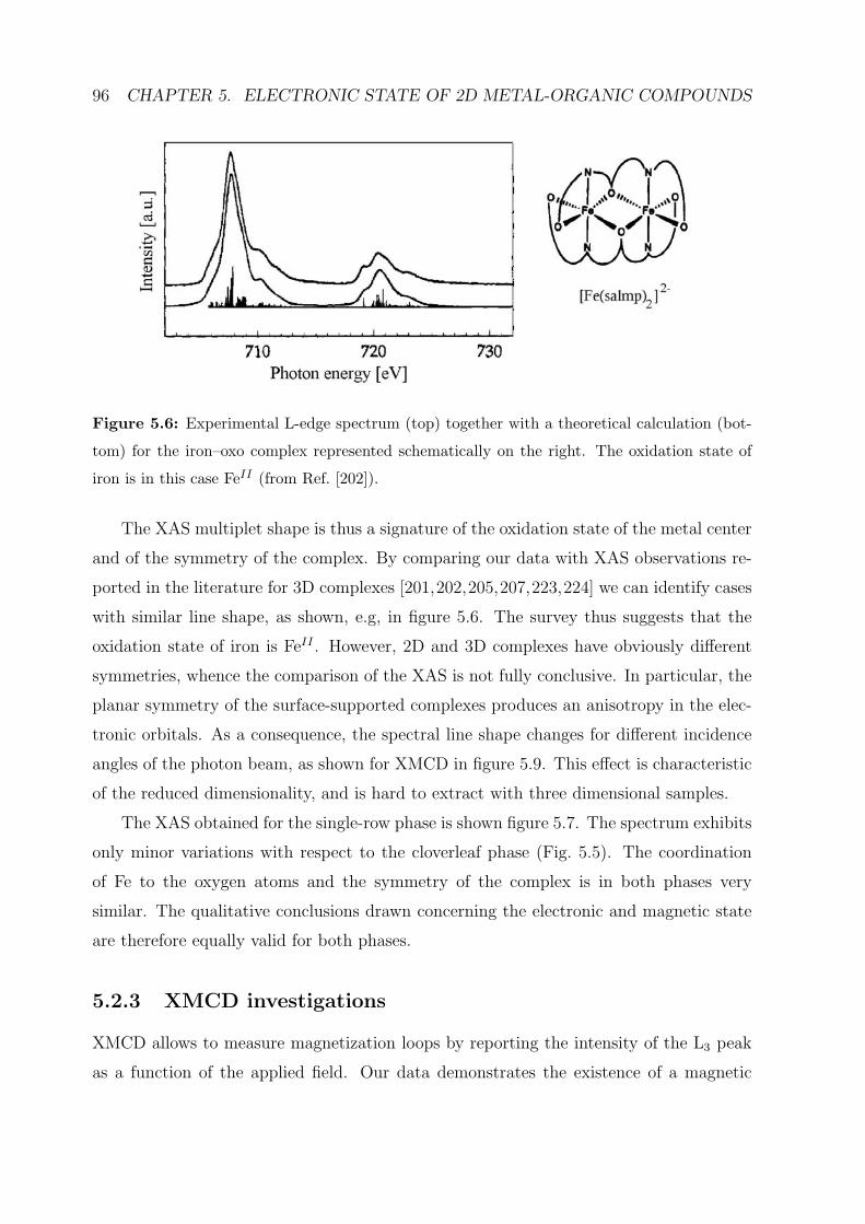
96 CHAPTER 5. ELECTRONIC STATE OF 2D METAL-ORGANIC COMPOUNDS
Figure 5.6: Experimental L-edge spectrum (top) together with a theoretical calculation (bot-
tom) for the iron–oxo complex represented schematically on the right. The oxidation state of
iron is in this case FeII (from Ref. [202]).
The XAS multiplet shape is thus a signature of the oxidation state of the metal center
and of the symmetry of the complex. By comparing our data with XAS observations re-
ported in the literature for 3D complexes [201,202,205,207,223,224] we can identify cases
with similar line shape, as shown, e.g, in figure 5.6. The survey thus suggests that the
oxidation state of iron is FeII . However, 2D and 3D complexes have obviously different
symmetries, whence the comparison of the XAS is not fully conclusive. In particular, the
planar symmetry of the surface-supported complexes produces an anisotropy in the elec-
tronic orbitals. As a consequence, the spectral line shape changes for different incidence
angles of the photon beam, as shown for XMCD in figure 5.9. This effect is characteristic
of the reduced dimensionality, and is hard to extract with three dimensional samples.
The XAS obtained for the single-row phase is shown figure 5.7. The spectrum exhibits
only minor variations with respect to the cloverleaf phase (Fig. 5.5). The coordination
of Fe to the oxygen atoms and the symmetry of the complex is in both phases very
similar. The qualitative conclusions drawn concerning the electronic and magnetic state
are therefore equally valid for both phases.
5.2.3 XMCD investigations
XMCD allows to measure magnetization loops by reporting the intensity of the L3 peak
as a function of the applied field. Our data demonstrates the existence of a magnetic
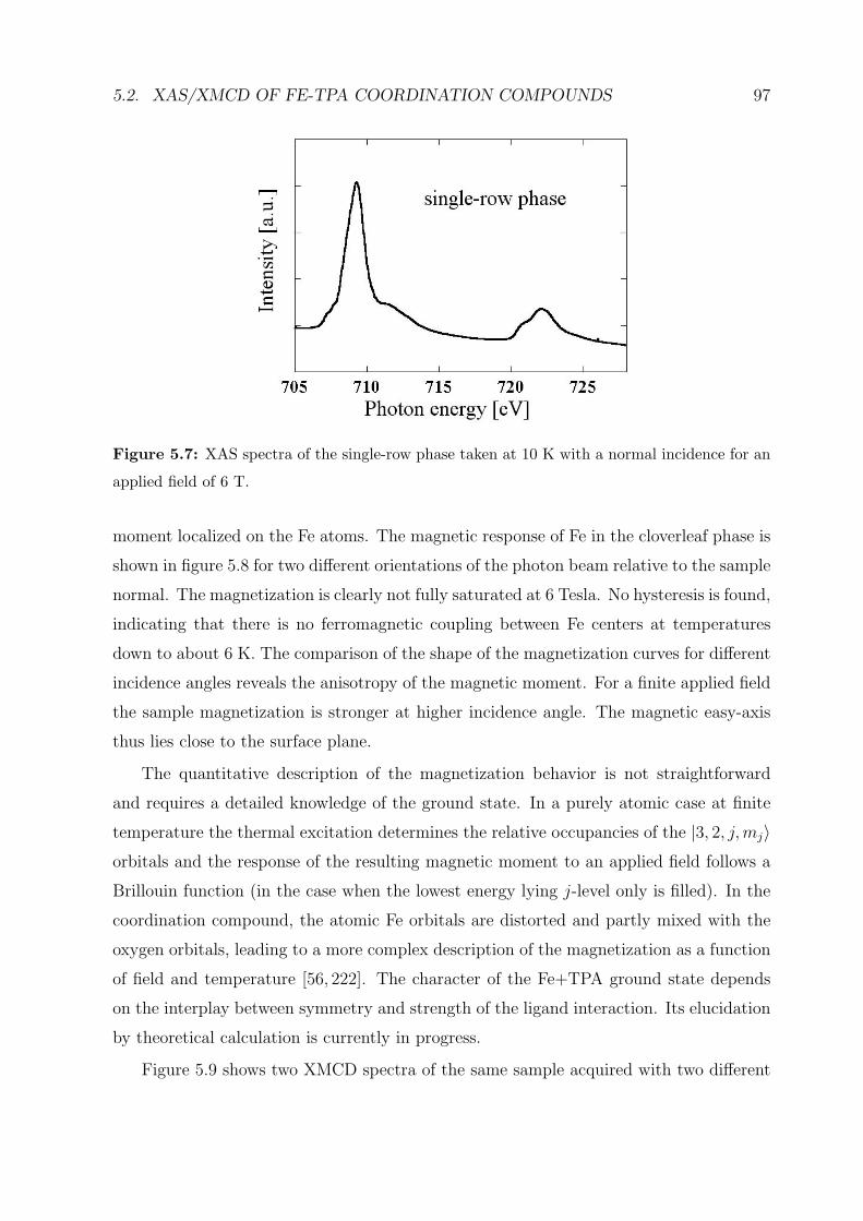
5.2. XAS/XMCD OF FE-TPA COORDINATION COMPOUNDS 97
Figure 5.7: XAS spectra of the single-row phase taken at 10 K with a normal incidence for an
applied field of 6 T.
moment localized on the Fe atoms. The magnetic response of Fe in the cloverleaf phase is
shown in figure 5.8 for two different orientations of the photon beam relative to the sample
normal. The magnetization is clearly not fully saturated at 6 Tesla. No hysteresis is found,
indicating that there is no ferromagnetic coupling between Fe centers at temperatures
down to about 6 K. The comparison of the shape of the magnetization curves for different
incidence angles reveals the anisotropy of the magnetic moment. For a finite applied field
the sample magnetization is stronger at higher incidence angle. The magnetic easy-axis
thus lies close to the surface plane.
The quantitative description of the magnetization behavior is not straightforward
and requires a detailed knowledge of the ground state. In a purely atomic case at finite
temperature the thermal excitation determines the relative occupancies of the |3, 2, j,mj〉orbitals and the response of the resulting magnetic moment to an applied field follows a
Brillouin function (in the case when the lowest energy lying j-level only is filled). In the
coordination compound, the atomic Fe orbitals are distorted and partly mixed with the
oxygen orbitals, leading to a more complex description of the magnetization as a function
of field and temperature [56, 222]. The character of the Fe+TPA ground state depends
on the interplay between symmetry and strength of the ligand interaction. Its elucidation
by theoretical calculation is currently in progress.
Figure 5.9 shows two XMCD spectra of the same sample acquired with two different
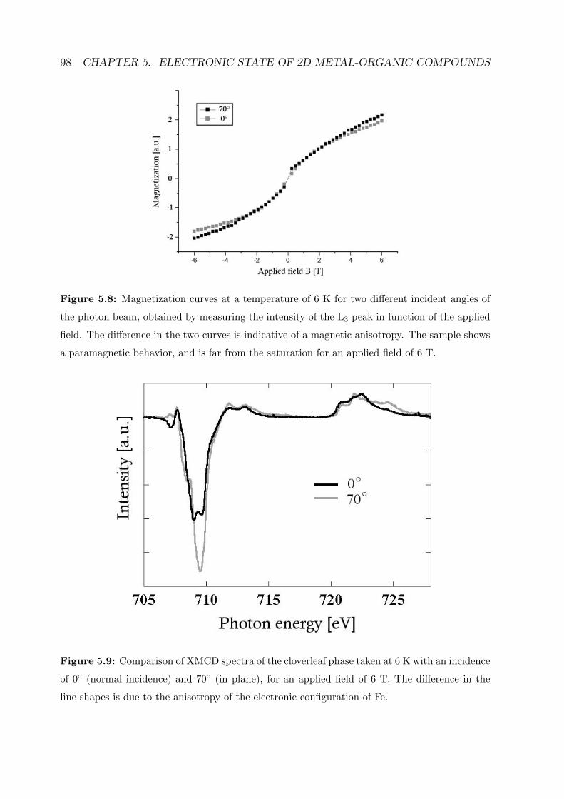
98 CHAPTER 5. ELECTRONIC STATE OF 2D METAL-ORGANIC COMPOUNDS
Figure 5.8: Magnetization curves at a temperature of 6 K for two different incident angles of
the photon beam, obtained by measuring the intensity of the L3 peak in function of the applied
field. The difference in the two curves is indicative of a magnetic anisotropy. The sample shows
a paramagnetic behavior, and is far from the saturation for an applied field of 6 T.
Figure 5.9: Comparison of XMCD spectra of the cloverleaf phase taken at 6 K with an incidence
of 0 (normal incidence) and 70 (in plane), for an applied field of 6 T. The difference in the
line shapes is due to the anisotropy of the electronic configuration of Fe.
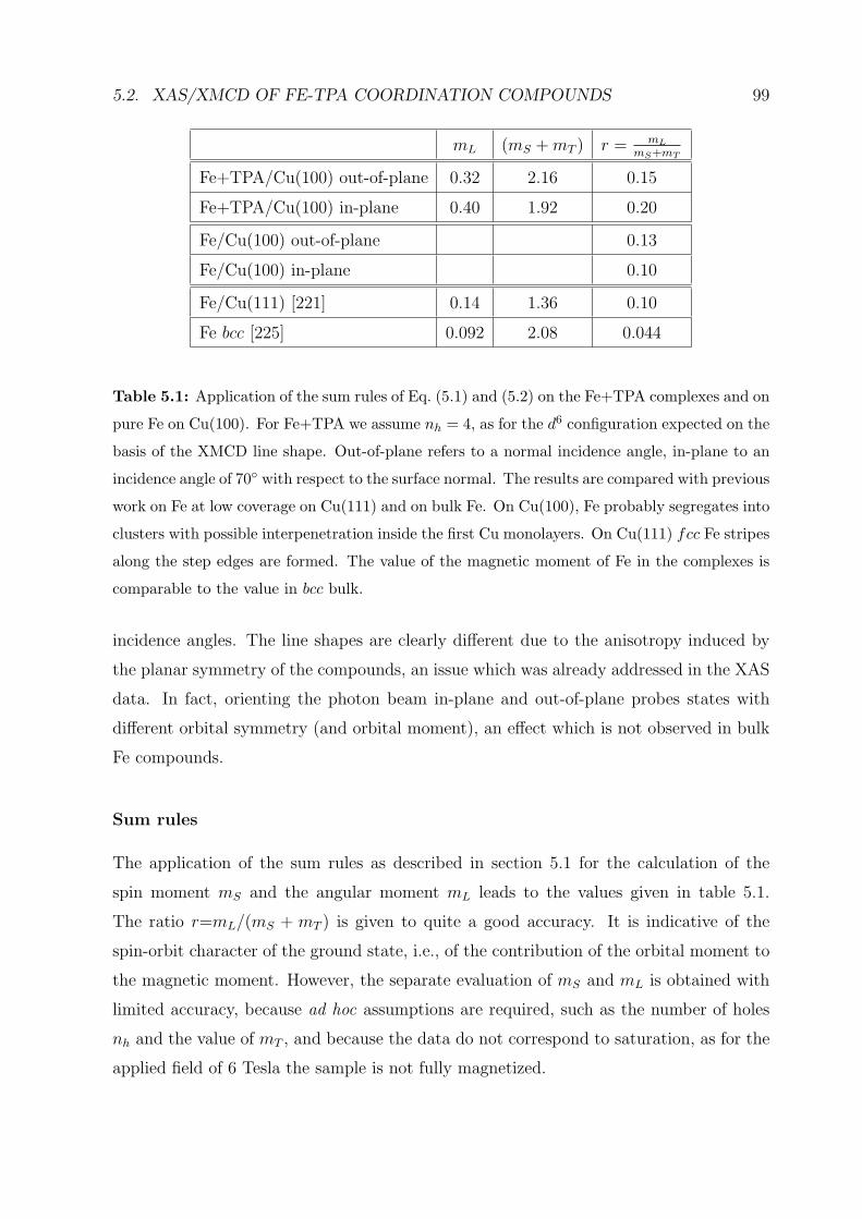
5.2. XAS/XMCD OF FE-TPA COORDINATION COMPOUNDS 99
mL (mS + mT ) r = mL
mS+mT
Fe+TPA/Cu(100) out-of-plane 0.32 2.16 0.15
Fe+TPA/Cu(100) in-plane 0.40 1.92 0.20
Fe/Cu(100) out-of-plane 0.13
Fe/Cu(100) in-plane 0.10
Fe/Cu(111) [221] 0.14 1.36 0.10
Fe bcc [225] 0.092 2.08 0.044
Table 5.1: Application of the sum rules of Eq. (5.1) and (5.2) on the Fe+TPA complexes and on
pure Fe on Cu(100). For Fe+TPA we assume nh = 4, as for the d6 configuration expected on the
basis of the XMCD line shape. Out-of-plane refers to a normal incidence angle, in-plane to an
incidence angle of 70 with respect to the surface normal. The results are compared with previous
work on Fe at low coverage on Cu(111) and on bulk Fe. On Cu(100), Fe probably segregates into
clusters with possible interpenetration inside the first Cu monolayers. On Cu(111) fcc Fe stripes
along the step edges are formed. The value of the magnetic moment of Fe in the complexes is
comparable to the value in bcc bulk.
incidence angles. The line shapes are clearly different due to the anisotropy induced by
the planar symmetry of the compounds, an issue which was already addressed in the XAS
data. In fact, orienting the photon beam in-plane and out-of-plane probes states with
different orbital symmetry (and orbital moment), an effect which is not observed in bulk
Fe compounds.
Sum rules
The application of the sum rules as described in section 5.1 for the calculation of the
spin moment mS and the angular moment mL leads to the values given in table 5.1.
The ratio r=mL/(mS + mT ) is given to quite a good accuracy. It is indicative of the
spin-orbit character of the ground state, i.e., of the contribution of the orbital moment to
the magnetic moment. However, the separate evaluation of mS and mL is obtained with
limited accuracy, because ad hoc assumptions are required, such as the number of holes
nh and the value of mT , and because the data do not correspond to saturation, as for the
applied field of 6 Tesla the sample is not fully magnetized.
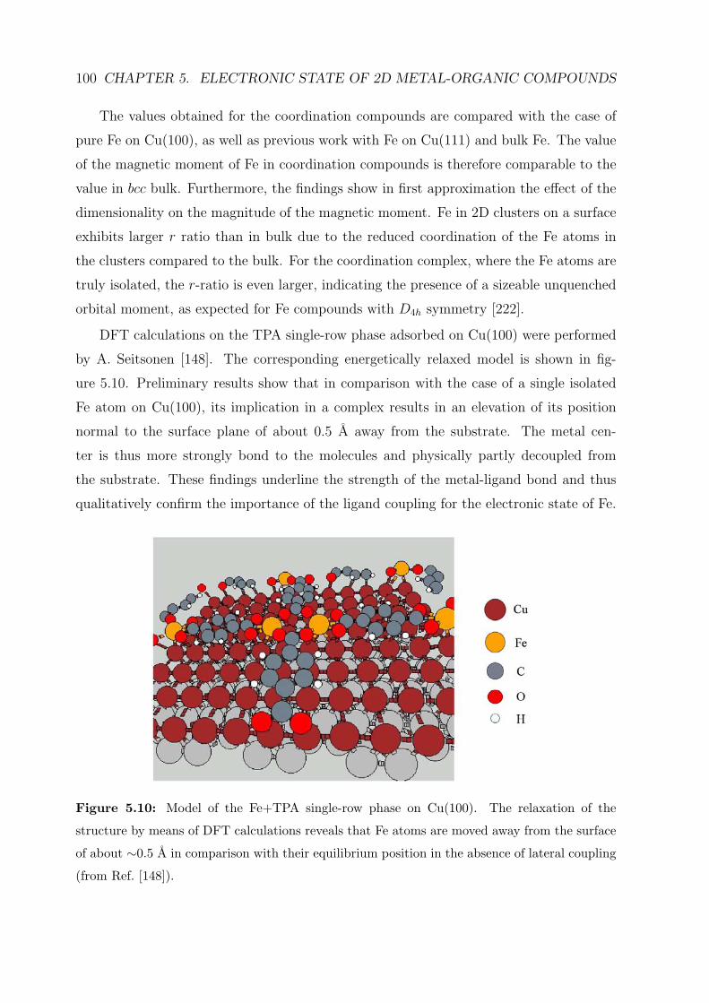
100 CHAPTER 5. ELECTRONIC STATE OF 2D METAL-ORGANIC COMPOUNDS
The values obtained for the coordination compounds are compared with the case of
pure Fe on Cu(100), as well as previous work with Fe on Cu(111) and bulk Fe. The value
of the magnetic moment of Fe in coordination compounds is therefore comparable to the
value in bcc bulk. Furthermore, the findings show in first approximation the effect of the
dimensionality on the magnitude of the magnetic moment. Fe in 2D clusters on a surface
exhibits larger r ratio than in bulk due to the reduced coordination of the Fe atoms in
the clusters compared to the bulk. For the coordination complex, where the Fe atoms are
truly isolated, the r-ratio is even larger, indicating the presence of a sizeable unquenched
orbital moment, as expected for Fe compounds with D4h symmetry [222].
DFT calculations on the TPA single-row phase adsorbed on Cu(100) were performed
by A. Seitsonen [148]. The corresponding energetically relaxed model is shown in fig-
ure 5.10. Preliminary results show that in comparison with the case of a single isolated
Fe atom on Cu(100), its implication in a complex results in an elevation of its position
normal to the surface plane of about 0.5 A away from the substrate. The metal cen-
ter is thus more strongly bond to the molecules and physically partly decoupled from
the substrate. These findings underline the strength of the metal-ligand bond and thus
qualitatively confirm the importance of the ligand coupling for the electronic state of Fe.
Figure 5.10: Model of the Fe+TPA single-row phase on Cu(100). The relaxation of the
structure by means of DFT calculations reveals that Fe atoms are moved away from the surface
of about ∼0.5 A in comparison with their equilibrium position in the absence of lateral coupling
(from Ref. [148]).
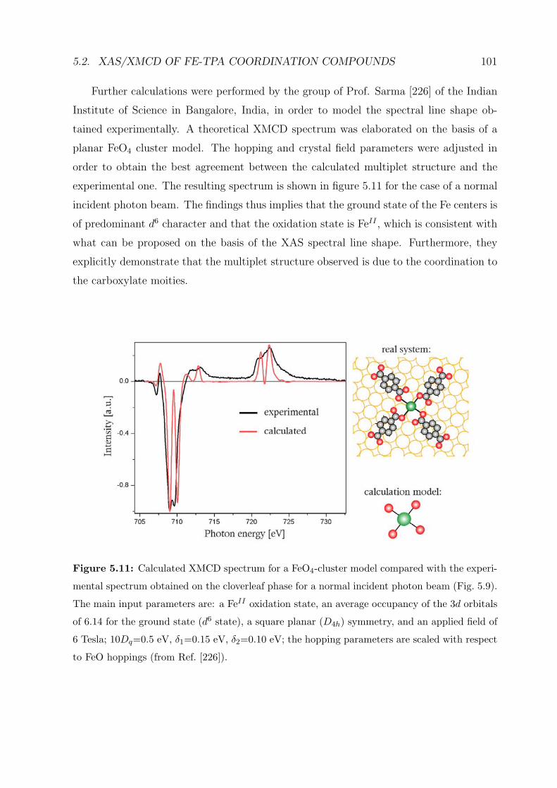
5.2. XAS/XMCD OF FE-TPA COORDINATION COMPOUNDS 101
Further calculations were performed by the group of Prof. Sarma [226] of the Indian
Institute of Science in Bangalore, India, in order to model the spectral line shape ob-
tained experimentally. A theoretical XMCD spectrum was elaborated on the basis of a
planar FeO4 cluster model. The hopping and crystal field parameters were adjusted in
order to obtain the best agreement between the calculated multiplet structure and the
experimental one. The resulting spectrum is shown in figure 5.11 for the case of a normal
incident photon beam. The findings thus implies that the ground state of the Fe centers is
of predominant d6 character and that the oxidation state is FeII , which is consistent with
what can be proposed on the basis of the XAS spectral line shape. Furthermore, they
explicitly demonstrate that the multiplet structure observed is due to the coordination to
the carboxylate moities.
Figure 5.11: Calculated XMCD spectrum for a FeO4-cluster model compared with the experi-
mental spectrum obtained on the cloverleaf phase for a normal incident photon beam (Fig. 5.9).
The main input parameters are: a FeII oxidation state, an average occupancy of the 3d orbitals
of 6.14 for the ground state (d6 state), a square planar (D4h) symmetry, and an applied field of
6 Tesla; 10Dq=0.5 eV, δ1=0.15 eV, δ2=0.10 eV; the hopping parameters are scaled with respect
to FeO hoppings (from Ref. [226]).
102 CHAPTER 5. ELECTRONIC STATE OF 2D METAL-ORGANIC COMPOUNDS
In conclusion, we could characterize the oxidation state of metals centers in surface-
supported architectures and identify the presence of a magnetic moment localized on
the Fe atoms. We have shown that the magnetic behavior and electronic ground state of
Fe+TPA deposited on a Cu substrate is primarily determined by the symmetry and nature
of the ligand rather than by the metallic substrate. This opens new opportunities to engi-
neer functional coordination architectures at surfaces. Supramolecular chemistry, with its
variety of functional bond combinations, can therefore be employed on surface-supported
metal-organic compounds to tailor their magnetic and electronic response, similarly to
what is done in bulk molecular crystals [56].
Conclusions and Future Directions
In the present thesis Low-Temperature Scanning Tunneling Microscopy (LT-STM) was
used to study supramolecular ensembles at well-defined metal surfaces. A major part
of the work was dedicated to the design and construction of a new experimental setup.
The performance and the excellent stability of the instrument is demonstrated. The in-
vestigations presented concern the two-dimensional supramolecular bonding and ordering
of terephthalic acid (TPA). The intermolecular interaction is governed by the formation
of hydrogen bonds through the dimerization of the carboxyl groups, similar to the bulk
crystal phase. The stability of the resulting supramolecular sheet is strongly influenced
by the peculiar structure of the surface plane. In the case of Au(111), the surface re-
construction causes distortions in the regular atomic arrangement which are transmitted
to the molecular layer. In particular, this induces appreciable variations in the hydrogen
bond length, which underlines the versatility of this non-covalent interaction for the for-
mation of supramolecular architectures. In the case of Cu(111) the commensurability to
the surface is not strictly possible and defects in the self-assembled layer are created.
Furthermore, we present the formation of surface-supported coordination compounds.
By taking advantage of the mesoscopic patterning of the reconstructed Au(111) surface
we succeed in creating nanoarchitectures governed by metal-ligand interactions. Nano-
and mesoscopic ordering is achieved by metallosupramolecular engineering. In addition,
the dynamics of the formation of metallosupramolecular nanogrids could be monitored in
situ, showing in particular their high thermodynamical stability in comparison with the
biphasic system made out of separated metal clusters and molecular 2D gas phase.
These results attest to the usefulness of STM as a tool for elucidating molecule-based
nanoarchitectures at surfaces. Its high resolution imaging ability allows for resolving the
precise organization of such systems, thus revealing key principles on the delicate balance
between molecule-molecule and molecule-substrate interactions which govern supramolec-
103
104 CONCLUSIONS AND FUTURE DIRECTIONS
ular assemblies on surfaces.
The magnetic and electronic properties of coordination compounds on the Cu(100)
surface were investigated by means of X-ray Absorption Spectroscopy (XAS) and X-ray
Magnetic Circular Dichroism (XMCD). The oxidation and valence state of Fe in metal-
organic compounds could be elucidated, showing the decisive influence of the ligand in
the ground state configuration of the metal center. The presence of a magnetic moment
located on the Fe atoms and the paramagnetic behavior of the system is demonstrated.
This result illustrates the great variety of options to effectively tailor the valence state
and magnetic moment of transition metal atoms at surfaces by the choice of appropriate
ligands and substrates.
Two principle ways can be envisioned for the further development of supramolecular
engineering on surfaces. On the one hand the continuation of structural studies, where
the rich arsenal of organic linkers and metals, accumulated by conventional solution and
solid state metal-organic chemistry, can be explored to construct novel supramolecular
architectures. In particular, the strong directionality of the metal-ligand bond could be
exploited further, together with molecules of different symmetry, size and functionality.
Furthermore, various kinds of surface pre-patterning can be obtained by stress-induced
metallic heteroepitaxial growth [227, 228]. Its utilization for directing supramolecular
organization is very encouraging, as was shown with Co and Fe on Au(111). A systematic
development of the genuine bottom-up strategy for the fabrication of novel self-assembled
structures is in this way expected to provide subtle control over the resulting topologies
at the nanoscale.
On the other hand a deeper understanding of the nature of the intermolecular bonds
at surfaces can be obtained. For this, the spectroscopic ability of STM can bring precious
information on the electronic state of self-assembled systems on a local scale. In particular,
inelastic spectroscopy (IETS) could deliver direct insight into the chemical nature of the
interactions involved at a single-bond level [229–233]. Moreover, when STM is employed
in combination with integral methods like X-ray absorption or X-ray photoemission spec-
troscopy, a comprehensive description can be gained. Additionally, the determination of
the electronic structure, the associated energies and the exact coordination geometries for
low-dimensional supramolecular architectures can be rationalized in depth by theoretical
calculations [84,234].
105
The metal-organic coordination networks presented in chapter 4 and related systems
are especially promising for future studies. In particular, their magnetic properties can
be better controlled. For the system Fe+TPA on Cu(100), the paramagnetic behavior
was shown. However, by an accurate choice of the molecule, the distance between the
magnetic centers could be reduced, thus possibly leading to a ferro- or antiferromagnetic
coupling. Another solution would be the use of molecular magnets which could mediate
magnetic coupling. Furthermore, the electronic properties of the one-dimensional Co-
TPA chain need to be investigated in details, by STS and IETS. In addition, the chemical
reactivity of the metal centers in coordination networks should be tested for applications
in heterogeneous catalysis. Finally, the functionality of the nano-cavities obtained can
be further developed in order to use them as chemically active sites for selective guest
accommodation.
Supramolecular science at surfaces is thus well positioned at the fertile border between
experimental physics, theoretical physics, material science, chemistry and biology. A close
interdisciplinary cooperation is required to make this field move forward!

Acknowledgements
I would like to thank my thesis director Prof. Johannes Barth for having given me the
opportunity to be his first Ph.D. student. I am very grateful in particular for his in-
volvement in the design of the new setup; his ideas and large competencies have been
very useful during my whole thesis work. I would like to thank furthermore Prof. Har-
ald Brune and Prof. Klaus Kern for the collaborations and their implication in the project.
I also want to thank the members of the jury, Prof. Michael Gratzel, Prof. Nacho
Pascual and Prof. Louis Porte for judging this thesis.
The whole technical team from the workshops at IPN in Lausanne, Pascal Cat-
tin, Gilles Grandjean, Philippe Guex, Philippe Zurcher, Andre Guisolan, Claude Blanc,
Philippe Cordey, Martial Doy, Jose Grandjean and Michel Fazan as well as Wolfgang
Stiepany from MPI in Stuttgart are gratefully acknowledged. Their respective skills have
been really appreciated and the quality of their work was decisive for the construction of
the experimental setup. Thanks also to Claire-Lise Bandelier, Andre Schlafli, Francoise
Jenny and Florence Choulat for the administrative support.
The synchrotron measurement week at ESRF became even pleasant thanks to the
presence of Pietro Gambardella, Sasha Dmitriev, Sebastian Stepanow and Jan Honolka,
as well as our local contacts Peter Bancock and Stefan Stanescu. Thanks in particular
to Pietro for his powerful skills on magnetism and X-ray things. I would also like to
thank Ari Seitsonen of the University Zurich for the DFT calculations, as well as my best
assistant Stephane Pons with whom I made all the STM measurements in Lausanne.
107

108
Getting to know about STM and nanoscience was done thanks to many other col-
leagues at IPN, among which Imad Arfaoui, Tristan Cren, Katharina Franke, Sarah Long-
witz, Stefano Rusponi, Nicolas Weiss and my office mates Marta Canas, Erik Delvigne,
Christian Klinke and Agustın Schriffrin. A special thank you goes to Olga for her help in
the English language.
Finally I would like to thank my family and friends who successfully managed to give
me regular and highly appreciated visits during my whole stay in Lausanne.
Bibliography
[1] C. M. Niemeyer, Angew. Chem. Int. Ed. 40, 4128 (2001).
[2] P. Moriarty, Rep. Prog. Phys. 64, 297 (2001).
[3] J.-M. Lehn, Supramolecular Chemistry (VCH, Weinheim, 1995).
[4] T. A. Jung, R. R. Schlittler, and J. K. Gimzewski, Nature 386, 696 (1997).
[5] M. Bohringer, K. Morgenstern, W.-D. Schneider, R. Berndt, F. Mauri, A. de Vita,
and R. Car, Phys. Rev. Lett. 83, 324 (1999).
[6] J. V. Barth, J. Weckesser, C. Cai, P. Gunter, L. Burgi, O. Jeandupeux, and K.
Kern, Angew. Chem. Int. Ed. 39, 1230 (2000).
[7] T. Yokoyama, S. Yokoyama, T. Kamikado, Y. Okuno, and S. Mashiko, Nature 413,
619 (2001).
[8] M. Schunack, L. Petersen, A. Kuhnle, E. Laegsgaard, I. Stensgaard, I. Johannsen,
and F. Besenbacher, Phys. Rev. Lett. 86, 456 (2001).
[9] F. Rosei, M. Schunack, P. Jiang, A. Gourdon, E. Laegsgaard, I. Stensgaard, C.
Joachim, and F. Besenbacher, Science 296, 328 (2002).
[10] K. W. Hipps, L. Scudiero, D. E. Barlow, and J. M. P. Cooke, J. Am. Chem. Soc.
124, 2126 (2002).
[11] J. A. Theobald, N. S. Oxtoby, M. A. Phillips, N. R. Champness, and P. H. Beton,
Nature 424, 1029 (2003).
[12] G. P. Lopinski, D. J. Moffatt, D. D. Wayner, and R. A. Wolkow, Nature 392, 909
(1998).
109
110 BIBLIOGRAPHY
[13] A. Kuhnle, T. R. Linderoth, B. Hammer, and F. Besenbacher, Nature 415, 891
(2002).
[14] J. V. Barth, J. Weckesser, G. Trimarchi, M. Vladimirova, A. de Vita, C. Cai, H.
Brune, P. Gunter, and K. Kern, J. Am. Chem. Soc. 124, 7991 (2002).
[15] T. Zambelli, J. V. Barth, J. Wintterlin, and G. Ertl, Nature 390, 495 (1997).
[16] G. A. Somorjai, J. Phys. Chem. B 106, 9201 (2002).
[17] M. Durr, A. Biedermann, Z. Hu, U. Hofer, and T. F. Heinz, Science 296, 1838
(2002).
[18] G. S. MacCarty and P. S. Weiss, J. Phys. Chem. B 106, 8005 (2002).
[19] W. Ho, J. Chem. Phys. 117, 11033 (2002).
[20] X.-C. Guo and R. J. Madix, J. Phys. Chem. B 107, 3105 (2003).
[21] M. O. Lorenzo, C. Baddeley, C. Muryn, and R. Raval, Nature 404, 376 (2000).
[22] J. Wintterlin, Adv. Catal. 45, 131 (2000).
[23] J. S. Lindsey, New J. Chem. 15, 153 (1991).
[24] G. M. Whitesides, P. J. Mathias, and C. T. Seto, Science 154, 1312 (1991).
[25] M. M. Conn and J. J. Rebek, Chem. Rev. 97, 1647 (1997).
[26] M. C. T. Fyfe and J. F. Stoddart, Coord. Chem. Rev. 183, 139 (1999).
[27] G. R. Desiraju, Crystal engineering : The design of organic solids (Elsevier, Ams-
terdam, 1989).
[28] B. Moulton and M. J. Zaworotko, Chem. Rev. 101, 1629 (2001).
[29] D. Braga, Chem. Commun. 22, 2751 (2003).
[30] F. Vogtle, Supramolecular Chemistry (Wiley, New York, 1991).
[31] Comprehensive Supramolecular Chemistry, edited by J. L. Atwood, J. E. D. Davies,
D. D. MacNicol, F. Vogtle, and J.-M. Lehn (Pergamon, New York, 1996).
BIBLIOGRAPHY 111
[32] G. A. Jeffrey and W. Saenger, Hydrogen Bonding in Biological Systems (Springer,
Berlin, 1991).
[33] L. J. Prins, D. N. Reinhoudt, and P. Timmerman, Angew. Chem. Int. Ed. 40, 2382
(2001).
[34] J.-H. Fournier, T. Maris, J. D. Wuest, W. Guo, and E. Galoppini, J. Am. Chem.
Soc. 125, 1002 (2003).
[35] T. Kawai, H. Tanaka, and T. Nakagawa, Surf. Sci. 386, 124 (1997).
[36] M. Furukawa, H. Tanaka, K.-I. Sugiura, Y. Sakata, and T. Kawai, Surf. Sci. Lett.
445, L58 (2000).
[37] J. Weckesser, A. de Vita, J. V. Barth, C. Cai, and K. Kern, Phys. Rev. Lett. 87,
096101 (2001).
[38] J. N. O’Shea, J. Schnadt, P. A. Bruhwiler, H. Hillesheimer, N. Martensson, L.
Patthey, J. Krempasky, C. Wang, Y. Luo, and H. Agren, J. Phys. Chem. B 105,
1917 (2001).
[39] T.-Q. Nguyen, M. L. Bushey, L. E. Brus, and C. Nuckolls, J. Am. Chem. Soc. 124,
15051 (2002).
[40] A. McNutt, S. Haq, and R. Raval, Surf. Sci. 531, 131 (2003).
[41] S. de Feyter and F. C. de Schryver, Chem. Soc. Rev. 32, 139 (2003).
[42] A. Werner, Z. Anorg. Chem. 3, 267 (1893).
[43] Comprehensive Coordination Chemistry, edited by G. Wilkinson, R. D. Gillard, and
J. A. McCleverty (Pergamon, Oxford, 1987).
[44] B. J. Holliday and C. A. Mirkin, Angew. Chem. Int. Ed. 40, 2022 (2001).
[45] M. Fujita, Chem. Soc. Rev. 27, 417 (1998).
[46] B. Olenyuk, J. A. Whiteford, A. Fechtenkotter, and P. J. Stang, Nature 398, 796
(1999).
112 BIBLIOGRAPHY
[47] M. E. Davis, Nature 417, 813 (2002).
[48] A. Stein, Adv. Mater. 15, 763 (2003).
[49] R. Vilar, Angew. Chem. Int. Ed. 42, 1460 (2003).
[50] V. Balzani, M. Venturi, and A. Credi, Molecular Devices and Machines (Wiley-
VCH, Weinheim, 2003).
[51] P. Ball, Nature 381, 648 (1996).
[52] D. Braga, F. Grepioni, and G. R. Desiraju, Chem. Rev. 98, 1375 (1998).
[53] J. M. Brown and S. G. Davies, Nature 342, 631 (1989).
[54] P. Serp and P. Kalck, Chem. Rev. 102, 3085 (2002).
[55] C. Coperet, M. Chabanas, R. P. Saint-Arroman, and J.-M. Basset, Angew. Chem.
Int. Ed. 42, 156 (2003).
[56] O. Kahn, Molecular Magnetism (Wiley-VCH, New York, 1993).
[57] A. Semenov, J. P. Spatz, M. Moller, J.-M. Lehn, B. Sell, D. Schubert, C. H. Weidl,
and U. S. Schubert, Angew. Chem. Int. Ed. 38, 2547 (1999).
[58] D. G. Kurth, N. Severin, and J. P. Rabe, Angew. Chem. Int. Ed. 41, 3681 (2002).
[59] S. Stepanow, M. Lingenfelder, A. Dmitriev, H. Spillmann, E. Delvigne, N. Lin, X.
Deng, C. Cai, J. V. Barth, and K. Kern, Nat. Mat. 3, 229 (2004).
[60] C. J. Chen, Introduction to Scanning Tunneling Microscopy (Oxford University
Press, New York, 1993).
[61] Scanning Tunneling Microscopy and Spectroscopy, edited by D. A. Bonnell (VCH,
New York, 1993).
[62] R. Wiesendanger, Scanning Probe Microscopy and Spectroscopy (Cambridge Uni-
versity Press, Cambridge, 1994).
[63] F. Besenbacher, Rep. Prog. Phys. 59, 1737 (1996).
BIBLIOGRAPHY 113
[64] S.-W. Hla and K.-H. Rieder, Annu. Rev. Phys. Chem. 54, 307 (2003).
[65] G. Binnig, H. Rohrer, C. Gerber, and E. Weibel, Phys. Rev. Lett. 49, 57 (1982).
[66] I. Giaever, Phys. Rev. Lett. 5, 147 (1960).
[67] J. Bardeen, Phys. Rev. Lett. 6, 57 (1961).
[68] J. Tersoff and D. H. Hamann, Phys. Rev. Lett. 50, 1998 (1983).
[69] A. Selloni, P. Carnevali, E. Tosatti, and C. D. Chen, Phys. Rev. B 31, 2602 (1985).
[70] N. D. Lang, Phys. Rev. B 34, 5947 (1986).
[71] G. Hormandinger, Phys. Rev. B 49, 13897 (1994).
[72] Y. Hasegawa and P. Avouris, Phys. Rev. Lett. 71, 1071 (1993).
[73] J. K. Gimzewski, E. Stoll, and R. R. Schlittler, Surf. Sci. 181, 267 (1987).
[74] H. Ohtani, R. J. Wilson, S. Chiang, and C. M. Mate, Phys. Rev. Lett. 60, 2398
(1988).
[75] P. H. Lippel, R. J. Wilson, M. D. Miller, C. Woll, and S. Chiang, Phys. Rev. Lett.
62, 171 (1989).
[76] C. J. Chen, J. Vac. Sci. Tec. A 9, 44 (1991).
[77] M. Tsukada, H. Kageshima, N. Isshiki, and K. Kobayashi, Surf. Sci. 266, 253 (1992).
[78] M. Tsukada, K. Kobayashi, N. Isshiki, H. Kageshima, T. Uchiyama, S. Watanabe,
and T. Schimizu, Surf. Sci. 287, 1004 (1993).
[79] G. Doyen, D. Drakova, J. V. Barth, R. Schuster, T. Gritsch, R. J. Behm, and G.
Ertl, Phys. Rev. B 48, 1738 (1993).
[80] P. Sautet and C. Joachim, Phys. Rev. B 38, 12238 (1988).
[81] R. F. Lin, G. S. Blackmann, M. A. van Hove, and G. A. Somorjai, Acta Cryst. B43,
368 (1987).
[82] P. Sautet and C. Joachim, Chem. Phys. Lett. 185, 23 (1991).
114 BIBLIOGRAPHY
[83] V. Hallmark, S. Chiang, K.-P. Mainhardt, and K. Hafner, Phys. Rev. Lett. 70, 3740
(1993).
[84] P. Sautet, Chem. Rev. 97, 1097 (1997).
[85] S. A. Elrod, L. de Lozanne, and C. F. Quate, Appl. Phys. Lett. 45, 1240 (1984).
[86] O. Marti, G. Binnig, H. Rohrer, and H. Salemink, Surf. Sci. 181, 230 (1987).
[87] H. F. Hess, R. B. Robinson, R. C. Dynes, J. M. Valles, and J. V. Waszczak, Phys.
Rev. Lett. 62, 214 (1989).
[88] R. Gaisch, J. K. Gimzewski, B. Reihl, R. R. Schlittler, M. Tschudy, and W.-D.
Schneider, Ultramicroscopy 42-44, 1621 (1992).
[89] S. Behler, M. K. Rose, J. C. Dunphy, D. F. Ogletree, M. Salmeron, and C. Chapelier,
Rev. Sci. Instr. 68, 2479 (1997).
[90] A. Hirstein, Ph.D. thesis, Ecole Polytechnique Federale de Lausanne, Switzerland,
1998.
[91] B. C. Stipe, M. A. Rezaei, and W. Ho, Rev. Sci. Instr. 70, 137 (1999).
[92] L. Petersen, M. Schunack, B. Schaefer, T. R. Linderoth, P. B. Rasmussen, P. T.
Sprunger, E. Laegsgaard, I. Stensgaard, and F. Besenbacher, Rev. Sci. Instr. 72,
1438 (2001).
[93] H.-P. Rust, M. Doering, J. I. Pascual, T. P. Pearl, and P. S. Weiss, Rev. Sci. Instr.
72, 4393 (2001).
[94] G. Meyer, Rev. Sci. Instr. 67, 2960 (1996).
[95] SPS-CreaTec GmbH, http://www.lt-stm.com/.
[96] Solidworks software, http://www.solidworks.com/.
[97] Melles Griot, http://www.mellesgriot.com/.
[98] Newport Corporation, http://www.newport.com/.
BIBLIOGRAPHY 115
[99] O. Jeandupeux, L. Burgi, A. Hirstein, H. Brune, and K. Kern, Phys. Rev. B 59,
15926 (1999).
[100] S. Pons, P. Mallet, L. Magaud, and J.-Y. Veuillen, Europhys. Lett. 61, 375 (2003).
[101] VAb Vakuumanlagenbau GmbH, http://www.vab-vakuum.de/.
[102] Turbovac 340M, Leybold Vakuum GmbH, http://www.leyboldvac.de/.
[103] St707 strips, SAES Getter SpA, http://www.saesgetters.com/.
[104] EFM 3, Omicron NanoTechnology GmbH, http://www.omicron.de/.
[105] A. Schiffrin, Ph.D. thesis, in prep.
[106] Cryovac GmbH & CoKG, http://www.cryovac.de/.
[107] Victor Kyburz AG, http://www.kyburz-sapphire.ch/.
[108] Lake Shore Cryotronics, Inc., http://www.lakeshore.com/.
[109] K. Besocke, Surf. Sci. 181, 145 (1987).
[110] J. Frohn, J. Wolf, K. Besocke, and M. Teske, Rev. Sci. Instr. 60, 1200 (1989).
[111] Epoxy Technology, http://www.epotek.com/.
[112] Staveley NDT Technologies, http://www.staveleyndt.com/.
[113] California Fine Wire Company, http://www.calfinewire.com/.
[114] Advent Research Materials Ltd, http://www.advent-rm.com/.
[115] S. Behler, M. K. Rose, D. F. Ogletree, and M. Salmeron, Rev. Sci. Instr. 68, 124
(1997).
[116] RHK Technology, Inc., http://www.rhk-tech.com/.
[117] Nanotec Electronica, http://www.nanotec.es/.
[118] S. D. Kevan and R. H. Gaylord, Phys. Rev. B 36, 5809 (1987).
[119] M. F. Crommie, C. P. Lutz, and D. M. Eigler, Nature 363, 524 (1993).
116 BIBLIOGRAPHY
[120] J. Li, W.-D. Schneider, R. Berndt, and S. Crampin, Phys. Rev. Lett. 80, 3332
(1998).
[121] S. Pons, P. Mallet, and J.-Y. Veuillen, Phys. Rev. B 64, 193408 (2001).
[122] L. Diekhoner, M. A. Schneider, A. N. Baranov, V. S. Stepanyuk, P. Bruno, and K.
Kern, Phys. Rev. Lett. 90, 236801 (2003).
[123] N. Memmel, Surf. Sci. Rep. 32, 91 (1998).
[124] O. M. Yaghi, M. O’Keeffe, N. W. Ockwing, H. K. Chae, M. Eddaoudi, and J. Kim,
Nature 423, 705 (2003).
[125] Y.-G. Kim, S.-L. Yau, and K. Itaya, Langmuir 15, 7810 (1999).
[126] N. Lin, A. Dmitriev, J. Weckesser, J. V. Barth, and K. Kern, Angew. Chem. Int.
Ed. 41, 4779 (2002).
[127] A. Dmitriev, N. Lin, J. Weckesser, J. V. Barth, and K. Kern, J. Phys. Chem. B
106, 6907 (2002).
[128] S. Griessl, M. Lackinger, M. Edelwirth, M. Hietschold, and W. M. Heckl, Single
Molecules 3, 25 (2002).
[129] A. Dmitriev, H. Spillmann, N. Lin, J. V. Barth, and K. Kern, Angew. Chem. Int.
Ed. 42, 2670 (2003).
[130] M. A. Lingenfelder, H. Spillmann, A. Dmitriev, S. Stepanow, N. Lin, J. V. Barth,
and K. Kern, Chem. Eur. J. 10, 1913 (2004).
[131] B. Bailey and C. J. Brown, Acta Cryst. 22, 387 (1967).
[132] M. Sledz, J. Janczak, and R. Kubiak, J. Mol. Struct. 595, 77 (2001).
[133] B. Parker, B. Immaraporn, and A. J. Gellman, Langmuir 17, 6638 (2001).
[134] J. V. Barth, H. Brune, R. J. Behm, and G. Ertl, Phys. Rev. B 42, 9307 (1990).
[135] D. S. Martin, R. J. Cole, and S. Haq, Phys. Rev. B 66, 155427 (2002).
BIBLIOGRAPHY 117
[136] J. V. Barth, J. Weckesser, N. Lin, A. Dmitriev, and K. Kern, Appl. Phys. A 76,
645 (2003).
[137] F. Mittendorfer and J. Hafner, Surf. Sci. 472, 133 (2001).
[138] P. A. Redhead, Vacuum 12, 203 (1962).
[139] S. M. Wetterer, D. J. Lavrich, T. Cummings, S. L. Bernasek, and G. Scoles, J. Phys.
Chem. B 102, 9266 (1998).
[140] A. R. Sandy, S. G. J. Mochrie, D. M. Zehner, K. G. Huang, and D. Gibbs, Phys.
Rev. B 43, 4667 (1991).
[141] S. Narasimhan and D. Vanderbilt, Phys. Rev. Lett. 69, 1564 (1992).
[142] J. V. Barth, R. J. Behm, and G. Ertl, Surf. Sci. 341, 62 (1995).
[143] D. Friebel, T. Mangen, B. Obliers, C. Schlaup, P. Broekmann, and K. Wandelt,
Langmuir 20, 2803 (2004).
[144] H. L. Meyerheim and T. Gloege, Chem. Phys. Lett. 326, 45 (2000).
[145] H. L. Meyerheim, T. Gloege, M. Sokolowski, E. Umbach, and P. Bauerle, Europhys.
Lett. 52, 144 (2000).
[146] M. Vladimirova, G. Trimarchi, A. Baldereschi, J. Weckesser, K. Kern, J. V. Barth,
and A. de Vita, Acta Mat. 52, 1589 (2004).
[147] S. Clair, S. Pons, A. P. Seitsonen, H. Brune, K. Kern, and J. V. Barth, J. Phys.
Chem. B (2004), in press.
[148] A. P. Seitsonen (unpublished).
[149] G. Kresse and J. Furthmuller, Phys. Rev. B 54, 11169 (1996).
[150] P. E. Blochl, Phys. Rev. B 50, 17953 (1994).
[151] G. Kresse and D. Joubert, Phys. Rev. B 59, 1758 (1999).
[152] G. R. Desiraju and T. Steiner, The Weak Hydrogen Bond (Oxford University Press,
Oxford, 1999).
118 BIBLIOGRAPHY
[153] T. Steiner, Angew. Chem. Int. Ed. 41, 48 (2002).
[154] G. R. Desiraju, Acc. Chem. Res. 35, 565 (2002).
[155] H. Spillmann, A. Dmitriev, N. Lin, P. Messina, J. V. Barth, and K. Kern, J. Am.
Chem. Soc. 125, 10725 (2003).
[156] J. V. Barth, R. J. Behm, and G. Ertl, Surf. Sci. Lett. 302, L319 (1994).
[157] Q. Chen and N. V. Richardson, Prog. Surf. Sci. 73, 59 (2003).
[158] S. Stepanow, T. Strunskus, M. Lingenfelder, A. Dmitriev, H. Spillmann, N. Lin,
J. V. Barth, C. Woll, and K. Kern, (2004), submitted.
[159] J. I. Pascual, J. V. Barth, G. Ceballos, G. Trimarchi, A. de Vita, K. Kern, and
H.-P. Rust, J. Chem. Phys. 120, 11367 (2004).
[160] C. C. Perry, S. Haq, B. G. Frederick, and N. V. Richardson, Surf. Sci. 409, 512
(1998).
[161] M. Wuhn, J. Weckesser, and C. Woll, Langmuir 17, 7605 (2001).
[162] M. Bohringer, R. Berndt, and W.-D. Schneider, Phys. Rev. B 55, 1384 (1997).
[163] X. Zhao, Z. Gai, R. G. Zhao, W. S. Yang, and T. Sakurai, Surf. Sci. Lett. 424, L347
(1999).
[164] X. Zhao, J. Am. Chem. Soc. 122, 12584 (2000).
[165] Q. Chen, D. J. Frankel, and N. V. Richardson, Langmuir 17, 8276 (2001).
[166] G. Frenking and N. Frohlich, Chem. Rev. 100, 717 (2000).
[167] L. R. MacGillivray, R. H. Groeneman, and J. L. Atwood, J. Am. Chem. Soc. 120,
2676 (1998).
[168] S. R. Batten and R. Robson, Angew. Chem. Int. Ed. 37, 1460 (1998).
[169] Y. Cui, O. R. Evans, H. L. Ngo, P. S. White, and W. Lin, Angew. Chem. Int. Ed.
41, 1159 (2002).
BIBLIOGRAPHY 119
[170] D. Maspoch, D. Ruiz-Molina, K. Wurst, N. Domingo, M. Cavallini, F. Biscarini, J.
Tejada, C. Rovira, and J. Veciana, Nat. Mat. 2, 190 (2003).
[171] C. P. Collier, E. W. Wong, M. Belohradsky, F. M. Raymo, J. F. Stoddart, P. J.
Kuekes, R. S. Williams, and J. R. Heath, Science 285, 391 (1999).
[172] G. P. Lopinski, D. D. M. Wayner, and R. A. Wolkow, Nature 406, 48 (2000).
[173] C. Joachim, C. Gimzewski, and A. Aviram, Nature 408, 541 (2000).
[174] J. A. Meyer, I. D. Baikie, E. Kopatzki, and R. J. Behm, Surf. Sci. Lett. 365, L647
(1996).
[175] B. Voigtlander, G. Meyer, and N. M. Amer, Surf. Sci. Lett. 255, L529 (1991).
[176] D. D. Chambliss, R. J. Wilson, and S. Chiang, Phys. Rev. Lett. 66, 1721 (1991).
[177] B. Voigtlander, G. Meyer, and N. M. Amer, Phys. Rev. B 44, 10354 (1991).
[178] J. Repp, F. Moresco, G. Meyer, and K.-H. Rieder, Phys. Rev. Lett. 85, 2981 (2000).
[179] N. Knorr, H. Brune, M. Epple, A. Hirstein, M. A. Schneider, and K. Kern, Phys.
Rev. B 65, 115420 (2002).
[180] F. Silly, M. Pivetta, M. Ternes, F. Patthey, J. P. Pelz, and W.-D. Schneider, Phys.
Rev. Lett. 92, 016101 (2004).
[181] M. Kurmoo, H. Kumagai, M. A. Green, B. W. Lovett, S. J. Blundell, A. Ardavan,
and J. Singleton, J. Solid State Chem. 159, 343 (2001).
[182] X.-L. Zhou, J. M. White, and B. E. Koel, Surf. Sci. 218, 201 (1989).
[183] L. C. Cune and M. Apostol, Phys. Lett. A 273, 117 (2000).
[184] H. Over, Y. D. Kim, A. P. Seitsonen, S. Wendt, E. Lundgren, M. Schmid, P. Varga,
A. Morgante, and G. Ertl, Science 287, 1474 (2000).
[185] J. Wang, C. Y. Fan, Q. Sun, K. Reuter, K. Jacobi, M. Scheffler, and G. Ertl, Angew.
Chem. Int. Ed. 42, 2151 (2003).
[186] T. M. Wallis, N. Nilius, and W. Ho, Phys. Rev. Lett. 89, 236802 (2002).
120 BIBLIOGRAPHY
[187] S. Folsch, P. Hyldgaard, R. Koch, and K. H. Ploog, Phys. Rev. Lett. 92, 056803
(2004).
[188] A. de Vita, private communication.
[189] V. F. Puntes, K. M. Krishnan, and P. Alivisatos, Appl. Phys. Lett. 78, 2187 (2001).
[190] S. Rusponi, T. Cren, N. Weiss, M. Epple, P. Buluschek, L. Claude, and H. Brune,
Nat. Mat. 2, 546 (2003).
[191] P. Gambardella, J. Phys.-Condens. Mat. 15, S2533 (2003).
[192] P. Gambardella, S. Rusponi, M. Veronese, S. S. Dhesi, C. Grazioli, A. Dallmeyer,
I. Cabria, R. Zeller, P. H. Dederichs, K. Kern, C. Carbone, and H. Brune, Science
300, 1130 (2003).
[193] C. T. Black, C. B. Murray, R. Sandstrom, and S. Sun, Science 290, 1131 (2000).
[194] H. Zeng, J. Li, J. P. Liu, Z. L. Wang, and S. Sun, Nature 420, 395 (2002).
[195] H. C. Manoharan, C. P. Lutz, and D. M. Eigler, Nature 403, 512 (2000).
[196] N. Nilius, T. M. Wallis, and W. Ho, Science 297, 1853 (2002).
[197] B. Moulton, J. Lu, R. Hajndl, S. Hariharan, and M. J. Zaworotko, Angew. Chem.
Int. Ed. 41, 2821 (2002).
[198] H. Srikanth, R. Hajndl, B. Moulton, and M. J. Zaworotko, J. Appl. Phys. 93, 7089
(2003).
[199] U. Ziener, J.-M. Lehn, A. Mourran, and M. Moller, Chem. Eur. J. 8, 951 (2002).
[200] A. Cornia, A. C. Fabretti, M. Pacchioni, L. Zobbi, D. Bonacchi, A. Caneschi, D.
Gatteschi, R. Biagi, U. del Pennino, V. de Renzi, L. Gurevich, and H. S. J. van der
Zant, Angew. Chem. Int. Ed. 42, 1645 (2003).
[201] F. M. F. de Groot and J. C. Fuggle, Phys. Rev. B 42, 5459 (1990).
[202] G. Peng, J. van Elp, H. Jang, L. Que, W. H. Armstrong, and S. P. Cramer, J. Am.
Chem. Soc. 117, 2515 (1995).
BIBLIOGRAPHY 121
[203] E. Breuning, M. Ruben, J.-M. Lehn, F. Renz, Y. Garcia, V. Ksenofontov, P. Gutlich,
E. Wegelius, and K. Rissanen, Angew. Chem. Int. Ed. 39, 2504 (2000).
[204] J. R. Galan-Mascaros and K. R. Dunbar, Angew. Chem. Int. Ed. 42, 2289 (2003).
[205] E. C. Wasinger, F. M. F. de Groot, B. Hedman, K. O. Hodgson, and E. I. Solomon,
J. Am. Chem. Soc. 125, 12894 (2003).
[206] G. van der Laan, B. T. Thole, G. A. Sawatzky, and M. Verdaguer, Phys. Rev. B
37, 6587 (1988).
[207] G. van der Laan and I. W. Kirkman, J. Phys.-Condens. Mat. 4, 4189 (1992).
[208] J. M. McCormick, R. C. Reem, and E. I. Solomon, J. Am. Chem. Soc. 113, 9066
(1991).
[209] S. J. George, J. van Elp, J. Chen, Y. Ma, C. T. Chen, J.-B. Park, M. W. W. Adams,
B. G. Searle, F. M. F. de Groot, J. C. Fuggle, and S. P. Cramer, J. Am. Chem. Soc.
114, 4426 (1992).
[210] H. Wang, G. Peng, L. M. Miller, E. M. Scheuring, S. J. George, M. R. Chance, and
S. P. Cramer, J. Am. Chem. Soc. 119, 4921 (1997).
[211] G. van der Laan, B. Thole, G. Sawatzky, J. B. Goedkoop, J. Fuggle, J. Esteva, R.
Karnatak, J. P. Remeika, and H. Dabkowska, Phys. Rev. B 34, 6529 (1986).
[212] J. Stohr, J. Magn. Magn. Mater. 200, 470 (1999).
[213] R. Wu and A. J. Freeman, J. Magn. Magn. Mater. 200, 498 (1999).
[214] C. Cohen-Tannoudji, B. Diu, and F. Laloe, Quantum Mechanics (Wiley, New York,
1997).
[215] C. T. Chen, Y. U. Idzerda, H.-J. Lin, N. V. Smith, G. Meigs, E. Chaban, G. H. Ho,
E. Pellegrin, and F. Sette, Phys. Rev. Lett. 75, 152 (1995).
[216] B. Thole, P. Carra, F. Sette, and G. van der Laan, Phys. Rev. Lett. 68, 1943 (1992).
[217] M. Altarelli, Phys. Rev. B 47, 597 (1993).
122 BIBLIOGRAPHY
[218] P. Carra, B. Thole, M. Altarelli, and X. Wang, Phys. Rev. Lett. 70, 694 (1993).
[219] R. Wu, D. Wang, and A. Freeman, Phys. Rev. Lett. 71, 3581 (1993).
[220] R. Wu and A. Freeman, Phys. Rev. Lett. 73, 1994 (1994).
[221] P. Ohresser, G. Ghiringhelli, O. Tjernberg, and N. B. Brookes, Phys. Rev. B 62,
5803 (2000).
[222] B. N. Figgis and M. A. Hitchman, Ligand Field Theory and Its Applications (Wiley-
VCH, New-York, 2000).
[223] G. van der Laan and B. T. Thole, Phys. Rev. B 43, 13401 (1991).
[224] J. Luning, F. Nolting, A. Scholl, H. Ohldag, J. W. Seo, J. Fompeyrine, J.-P. Locquet,
and J. Stohr, Phys. Rev. B 67, 214433 (2003).
[225] D. Bonnenberg, K. A. Hempel, and H. P. J. Wijn, in Landolt-Bornstein, New se-
ries, edited by K.-H. Hellwege and O. Madelung (Springer-Verlag, Berlin, 1986),
Vol. III/19a, p. 178.
[226] S. S. Gupta and D. D. Sarma (unpublished).
[227] H. Brune, M. Giovannini, K. Bromann, and K. Kern, Nature 394, 451 (2000).
[228] V. Repain, G. Baudot, H. Ellmer, and S. Rousset, Europhys. Lett. 58, 730 (2002).
[229] B. Stipe, M. Rezaei, and W. Ho, Phys. Rev. Lett. 82, 1724 (1999).
[230] F. Moresco, G. Meyer, and K.-H. Rieder, Mod. Phys. Lett. B 13, 709 (1999).
[231] J. I. Pascual, J. J. Jackiw, Z. Song, P. S. Weiss, H. Conrad, and H.-P. Rust, Phys.
Rev. Lett. 86, 1050 (2001).
[232] Y. Kim, T. Komeda, and M. Kawai, Phys. Rev. Lett. 89, 126104 (2002).
[233] N. Lorente, Appl. Phys. A 78, 799 (2004).
[234] J. Hafner, Acta Mat. 48, 71 (2000).
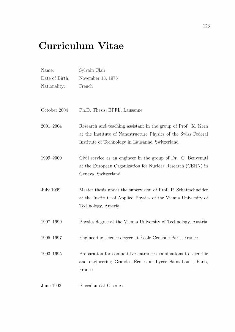
123
Curriculum Vitae
Name: Sylvain Clair
Date of Birth: November 18, 1975
Nationality: French
October 2004 Ph.D. Thesis, EPFL, Lausanne
2001–2004 Research and teaching assistant in the group of Prof. K. Kern
at the Institute of Nanostructure Physics of the Swiss Federal
Institute of Technology in Lausanne, Switzerland
1999–2000 Civil service as an engineer in the group of Dr. C. Benvenuti
at the European Organization for Nuclear Research (CERN) in
Geneva, Switzerland
July 1999 Master thesis under the supervision of Prof. P. Schattschneider
at the Institute of Applied Physics of the Vienna University of
Technology, Austria
1997–1999 Physics degree at the Vienna University of Technology, Austria
1995–1997 Engineering science degree at Ecole Centrale Paris, France
1993–1995 Preparation for competitive entrance examinations to scientific
and engineering Grandes Ecoles at Lycee Saint-Louis, Paris,
France
June 1993 Baccalaureat C series


![Template for Electronic Submission to ACS Journals · Web view]urils as excipients in pharmaceutical dosage forms. Supramol. Chem. 28, 849–856 (2016). 20.Sonzini, S. et al. Supramolecular](https://static.fdocuments.net/doc/165x107/608072b0df25ce1b0b54d17f/template-for-electronic-submission-to-acs-journals-web-view-urils-as-excipients.jpg)


