Investigation and Design of a Slotted Waveguide...
121
Investigation and Design of a Slotted Waveguide Antenna with Low 3D Sidelobes by Andries Johannes Nicolaas Maritz Thesis presented in partial fulfilment of the requirements for the degree of Master of Science in Engineering at Stellenbosch University Supervisor: Prof. Keith D. Palmer Department Electrical and Electronic Engineering March 2010
Transcript of Investigation and Design of a Slotted Waveguide...

Investigation and Design of a SlottedWaveguide Antenna with Low 3D
Sidelobes
by
Andries Johannes Nicolaas Maritz
Thesis presented in partial fulfilment of therequirements for the degree of
Master of Science in Engineeringat Stellenbosch University
Supervisor:
Prof. Keith D. Palmer
Department Electrical and Electronic Engineering
March 2010

Declaration
By submitting this thesis electronically, I declare that the entirety of the workcontained therein is my own, original work, that I am the owner of the copy-right thereof (unless to the extent explicitly otherwise stated) and that I havenot previously in its entirety or in part submitted it for obtaining any quali-fication.
March 2010
Copyright © 2010 Stellenbosch UniversityAll rights reserved

Abstract
An investigation into the cause of undesired sidelobes in the 3D radiationpattern of slotted waveguide arrays is conducted. It is hypothesized thatthe cross-polarization of the antenna is at fault, along with the possibilitythat an error is made when designing a linear array. In investigating andfinding a solution to the problem, the “Z-slot ” is introduced in conjunctionwith polarizer plates. The base components are used by a custom optimiza-tion algorithm to design reference and solution antennas. Results of theantennas are then compared to ascertain the cause and possible solutionsfor the unwanted sidelobes. The generic nature of the process may be usedto characterize other arbitrary aperture configurations and to design largerantennas.
iii

Opsomming
‘n Ondersoek om die oorsaak van ongewensde sylobbe in die 3D uitstraal-patroon van golfleier-antennas vas te stel. Die hipotese is dat die probleemontstaan uit die kruis-polarisasie van die antenna, tesame met ‘n verkeerde-likke aanname dat die opstelling liniêr is. Die “Z-Gleuf” tesame met po-lariseringsplate word voorgestel as hulpmiddel om die moontlikke oorsakete ondersoek. ‘n Gespesialiseerde optime erings-algoritme benut hierdie ba-siskomponente om beide verwysings- en oplossing-antennas te ontwerp.Resultate van die ontwerpde antennas word dan vergelyk om die oorsaakvan die ongewensde sylobbe te vas te stel. Die generiese aard van die proseskan toegepas word op enige gleuf-konfigurasie en om groter antennas meete ontwerp.
iv

Acknowledgements
The author would like to thank the following people for their contributiontowards this project.
• Prof K.D. Palmer
• Werner Steyn
• Jonathan Hoole
v

Contents
Abstract iii
Opsomming iv
Acknowledgements v
Contents vi
Abbreviations ix
List of Figures x
List of Tables xv
1 Introduction 11.1 Problem Statement . . . . . . . . . . . . . . . . . . . . . . . . . 11.2 Project Overview . . . . . . . . . . . . . . . . . . . . . . . . . . 31.3 Thesis Outline . . . . . . . . . . . . . . . . . . . . . . . . . . . . 4
2 Literature Study 62.1 Waveguides . . . . . . . . . . . . . . . . . . . . . . . . . . . . . 62.2 Aperture Antennas . . . . . . . . . . . . . . . . . . . . . . . . . 152.3 Transmission Line Theory . . . . . . . . . . . . . . . . . . . . . 192.4 Array Synthesis . . . . . . . . . . . . . . . . . . . . . . . . . . . 222.5 Waveguide Slot Arrays . . . . . . . . . . . . . . . . . . . . . . . 23
3 Design of the Waveguide Transmission Line 253.1 Waveguide Specifications . . . . . . . . . . . . . . . . . . . . . 253.2 Properties of Rectangular Waveguides . . . . . . . . . . . . . . 263.3 Design of a Ridged Waveguide . . . . . . . . . . . . . . . . . . 27
4 Analysis of Aperture Radiators 324.1 Discussion of Slot Properties of Interest . . . . . . . . . . . . . 324.2 Study: Offset Rectangular Aperture in the Broadwall . . . . . . 344.3 Study: Z-slot Aperture in the Broadwall . . . . . . . . . . . . . 35
vi

CONTENTS vii
4.4 Study: Z-slot Aperture in the Broadwall with Polarizer Plates . 374.5 Study: Z-slot Aperture in a Ridged Waveguide . . . . . . . . . 384.6 Study: Z-slot Aperture in a Ridged Waveguide with Polarizer
Plates . . . . . . . . . . . . . . . . . . . . . . . . . . . . . . . . . 394.7 Study: Varying Polarizer Plate Lengths in a Z-slot Ridged
Waveguide Configuration . . . . . . . . . . . . . . . . . . . . . 404.8 Equivalent Circuit Models . . . . . . . . . . . . . . . . . . . . . 444.9 Simulation Results . . . . . . . . . . . . . . . . . . . . . . . . . 45
5 Algorithms for Aperture Characterization & Antenna Optimiza-tion 475.1 Discussion of the Parameter Sweep Algorithm . . . . . . . . . 475.2 Extraction of Impedance Properties from S-Parameters . . . . 495.3 Simulation Results of a Parameter Sweep . . . . . . . . . . . . 535.4 Optimization Algorithm . . . . . . . . . . . . . . . . . . . . . . 565.5 Validation of CST Models . . . . . . . . . . . . . . . . . . . . . 65
6 Antenna Designs and Comparison 686.1 Benchmark Design . . . . . . . . . . . . . . . . . . . . . . . . . 686.2 WR75 Z-slot Antenna Design . . . . . . . . . . . . . . . . . . . 736.3 Ridged Waveguide Z-slot Antenna Design . . . . . . . . . . . . 786.4 Comparison of Benchmark and Z-slot Antenna Properties . . . 83
7 Conclusions 887.1 Summary . . . . . . . . . . . . . . . . . . . . . . . . . . . . . . . 887.2 Recommendations for Future Research . . . . . . . . . . . . . . 897.3 Conclusion . . . . . . . . . . . . . . . . . . . . . . . . . . . . . . 90
Appendices 91
A Benchmark Design 92A.1 Introduction . . . . . . . . . . . . . . . . . . . . . . . . . . . . . 92A.2 Dimensions . . . . . . . . . . . . . . . . . . . . . . . . . . . . . . 92A.3 Simulated Results . . . . . . . . . . . . . . . . . . . . . . . . . . 93
B WR75 Waveguide Z-slot Design 95B.1 Introduction . . . . . . . . . . . . . . . . . . . . . . . . . . . . . 95B.2 Dimensions . . . . . . . . . . . . . . . . . . . . . . . . . . . . . . 95B.3 Simulated Results . . . . . . . . . . . . . . . . . . . . . . . . . . 96
C Ridged Waveguide Z-slot Design 98C.1 Introduction . . . . . . . . . . . . . . . . . . . . . . . . . . . . . 98C.2 Dimensions . . . . . . . . . . . . . . . . . . . . . . . . . . . . . . 98C.3 Simulated Results . . . . . . . . . . . . . . . . . . . . . . . . . . 100

CONTENTS viii
D WR90 to Ridged Waveguide Transition 102
Bibliography 105

Abbreviations
• TE – Transverse Electric
• TM – Transverse Magnetic
• TEM – Transverse Electromagnetic
• CST – CST Microwave Studio (software tool)
• E-Field – Electric Field
• H-Field – Magnetic Field
• λ0 – Free-Space Wavelength
• f0 – Operating Frequency
• λG – Waveguide Wavelength
ix

List of Figures
1.1 Azimuth Depiction of Radiation Pattern for an Antenna Array . . 21.2 3D Radiation Pattern of a Slotted Waveguide Antenna . . . . . . . 2
2.1 Axis System for Arbitrary Transmission Lines and an Example ofa Transmission Mode . . . . . . . . . . . . . . . . . . . . . . . . . . 7(a) Axis System for Generic Waveguides . . . . . . . . . . . . . 7(b) TE10 Propagation Mode in a Rectangular Waveguide . . . . 7
2.2 Parallel Plate Transmission Line . . . . . . . . . . . . . . . . . . . . 82.3 Attenuation and Propagation Constant as a Function of Frequency 92.4 Rectangular Waveguide Dimensions and Axis System . . . . . . . 102.5 First Modes and their Cutoff Frequencies Found for the WR90
Waveguide Profile . . . . . . . . . . . . . . . . . . . . . . . . . . . . 11(a) TE10: fc = at 6.55 GHz . . . . . . . . . . . . . . . . . . . . . . 11(b) TE20: fc = at 13.07 GHz . . . . . . . . . . . . . . . . . . . . . 11(c) TE01: fc = at 14.73 GHz . . . . . . . . . . . . . . . . . . . . . 11(d) TE11: fc = at 16.12 GHz . . . . . . . . . . . . . . . . . . . . . 11(e) TM11: fc = at 16.12 GHz . . . . . . . . . . . . . . . . . . . . . 11(f) TM21: fc = at 19.69 GHz . . . . . . . . . . . . . . . . . . . . . 11
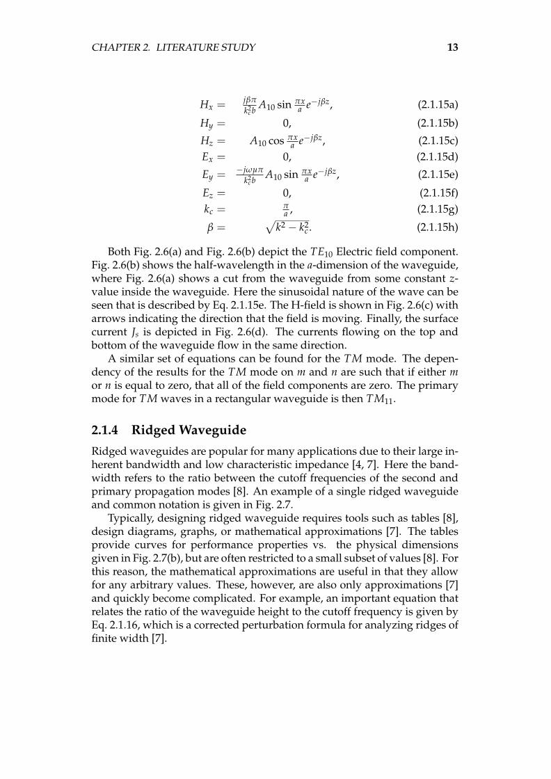
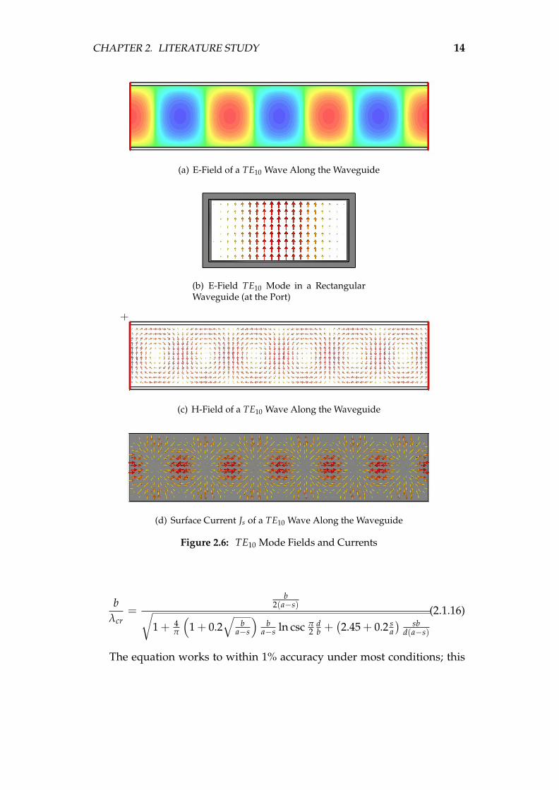
2.6 TE10 Mode Fields and Currents . . . . . . . . . . . . . . . . . . . . 14(a) E-Field of a TE10 Wave Along the Waveguide . . . . . . . . 14(b) E-Field TE10 Mode in a Rectangular Waveguide (at the Port) 14(c) H-Field of a TE10 Wave Along the Waveguide . . . . . . . . 14(d) Surface Current Js of a TE10 Wave Along the Waveguide . . 14
2.7 Single-Ridged Waveguide . . . . . . . . . . . . . . . . . . . . . . . 15(a) Single-Ridged Waveguide . . . . . . . . . . . . . . . . . . . . 15(b) Profile and Notation of a Single-Ridged Waveguide . . . . . 15
2.8 An Aperture Cut in a Screen with its Complementary Component 162.9 Aperture Excitation and Transmission Line Model . . . . . . . . . 172.10 Equivalent Circuit Models for Offset and Rotated Aperture An-
tennas . . . . . . . . . . . . . . . . . . . . . . . . . . . . . . . . . . . 18(a) Offset Aperture Antenna and its Equivalent Circuit Model . 18(b) Rotated Aperture Antenna and its Equivalent Circuit Model 18
2.11 Cascaded ABCD Parameters . . . . . . . . . . . . . . . . . . . . . . 192.12 Two-Port ABCD Network . . . . . . . . . . . . . . . . . . . . . . . 19
x

LIST OF FIGURES xi
2.13 ABCD Representation of a Transmission Line . . . . . . . . . . . . 202.14 ABCD Representation of a Series Impedance . . . . . . . . . . . . 212.15 ABCD Representation of a Parallel Admittance . . . . . . . . . . . 212.16 Example of a Cascaded ABCD Network . . . . . . . . . . . . . . . 212.17 Element Excitations for Two 40 Element Arrays . . . . . . . . . . . 22
(a) 40 Element Tschebyscheff Excitation . . . . . . . . . . . . . . 22(b) 40 Element Villeneuve Excitation . . . . . . . . . . . . . . . . 22
3.1 Depiction of Waveguide Specifications . . . . . . . . . . . . . . . . 263.2 Standard Rectangular Waveguide . . . . . . . . . . . . . . . . . . . 263.3 Single-Ridged Waveguide . . . . . . . . . . . . . . . . . . . . . . . 27
(a) Single-Ridged Waveguide . . . . . . . . . . . . . . . . . . . . 27(b) Profile and Notation of a Single-Ridged Waveguide . . . . . 27
3.4 Cutoff Frequencies of a Ridged Waveguide with a Fixed a and b . 29(a) Lower Cutoff Frequencies . . . . . . . . . . . . . . . . . . . . 29(b) Higher Cutoff Frequencies . . . . . . . . . . . . . . . . . . . 29
3.5 Region Where Both the Lower and Higher Cutoff FrequencySpecifications are Met . . . . . . . . . . . . . . . . . . . . . . . . . . 30
3.6 Physical Dimensions of Final Ridged Waveguide . . . . . . . . . . 30
4.1 Definition of Amplitude Tuners . . . . . . . . . . . . . . . . . . . . 334.2 Model for Rectangular Aperture at Some Offset from the Center-
line of the Waveguide . . . . . . . . . . . . . . . . . . . . . . . . . . 34(a) 3D Wireframe of Aperture . . . . . . . . . . . . . . . . . . . . 34(b) Top View of Aperture in Waveguide . . . . . . . . . . . . . . 34
4.3 Model for Z-slot at Some Rotation Angle . . . . . . . . . . . . . . . 36(a) 3D Wireframe of Aperture . . . . . . . . . . . . . . . . . . . . 36(b) Top View of Aperture in Waveguide . . . . . . . . . . . . . . 36
4.4 Model for Z-slot with 10mm Polarizer Plates . . . . . . . . . . . . 37(a) 3D Wireframe of Aperture . . . . . . . . . . . . . . . . . . . . 37(b) Top View of Aperture in Waveguide . . . . . . . . . . . . . . 37
4.5 Model for Z-slot in a Ridged Waveguide . . . . . . . . . . . . . . . 38(a) 3D Wireframe of Aperture . . . . . . . . . . . . . . . . . . . . 38(b) Top View of Aperture in Waveguide . . . . . . . . . . . . . . 38
4.6 Model for Z-slot with 10mm Polarizer Plates in a Ridged Waveg-uide . . . . . . . . . . . . . . . . . . . . . . . . . . . . . . . . . . . . 40(a) 3D Wireframe of Aperture . . . . . . . . . . . . . . . . . . . . 40(b) Top View of Aperture in Waveguide . . . . . . . . . . . . . . 40
4.7 Cross-Polarization Level with Varying Polarizer Plate Lengths . . 414.8 Bandwidth Variation as a Result of Varying Polarizer Plate Lengths 424.9 Radiated Power and Q-Factor for Varying Polarizer Plate Lengths 43
(a) Percentage of Power Radiated at f0 for Varying PolarizerPlate Lengths . . . . . . . . . . . . . . . . . . . . . . . . . . . 43
(b) Quality Factor at f0 for Varying Polarizer Plate Lengths . . . 43

LIST OF FIGURES xii
4.10 Phase of S11 for an Offset Aperture and a Z-slot . . . . . . . . . . 444.11 Percentage Bandwidth . . . . . . . . . . . . . . . . . . . . . . . . . 454.12 Percentage of Power Radiated by Aperture . . . . . . . . . . . . . 464.13 dB Cross-Polarization Level . . . . . . . . . . . . . . . . . . . . . . 46
5.1 Flow Chart of the Parameter Sweep . . . . . . . . . . . . . . . . . . 485.2 Z-slot Environment and Port Definitions . . . . . . . . . . . . . . . 49
(a) Z-slot Calibration Model for the Parameter Sweep . . . . . . 49(b) Port Locations Between Apertures and their Normal Direc-
tions . . . . . . . . . . . . . . . . . . . . . . . . . . . . . . . . 495.3 Location of Aperture Impedances With Respect to the Load
Impedance . . . . . . . . . . . . . . . . . . . . . . . . . . . . . . . . 535.4 Resistance: Real Part of the Aperture Impedance . . . . . . . . . . 535.5 Reactance: Imaginary Part of the Aperture Impedance . . . . . . . 545.6 Phase Slope: Rate with which Impedance Changes . . . . . . . . . 555.7 Phase of the Impedance . . . . . . . . . . . . . . . . . . . . . . . . 555.8 Flow Chart of the Optimization Algorithm . . . . . . . . . . . . . 565.9 Transmission Line Model for a Z-slot Antenna . . . . . . . . . . . 57
(a) Equivalent Transmission Line Model of a Z-slot Antenna . . 57(b) Reduced Transmission Line Model of a Z-slot Antenna . . . 57(c) Depiction of Argument for Reduced Transmission Line
Model . . . . . . . . . . . . . . . . . . . . . . . . . . . . . . . 575.10 Villeneuve Power and Impedance Distribution . . . . . . . . . . . 585.11 Magnitude and Phase of Electric Field over the Antenna . . . . . 60
(a) Magnitude of Ex of the Electric Field Over the Antenna . . . 60(b) Phase of Ex of the Electric Field Over the Antenna . . . . . . 60
5.12 Series Impedance Transmission Line Model Notation . . . . . . . 615.13 Curve Fitted to Simulated Data . . . . . . . . . . . . . . . . . . . . 625.14 Prediction Grids Before and After Adaptation . . . . . . . . . . . . 63
(a) Original Prediction Grid . . . . . . . . . . . . . . . . . . . . . 63(b) Adapted Prediction Grid . . . . . . . . . . . . . . . . . . . . 63
5.15 Gain Patterns for 40 Element Offset Rectangular Aperture Array . 665.16 Zoom of Gain Patterns for 40 Element Offset Rectangular Aper-
ture Array . . . . . . . . . . . . . . . . . . . . . . . . . . . . . . . . 67
6.1 CST Model of the Benchmark Template and Antenna . . . . . . . 69(a) Template Used to Generate the Antenna . . . . . . . . . . . 69(b) Antenna Generated by Optimization Algorithm . . . . . . . 69
6.2 Simulated Magnitudes for All Iterations of the Benchmark Antenna 70(a) Simulated Magnitudes Over All Iterations . . . . . . . . . . 70(b) Simulated Magnitude for Final Iteration . . . . . . . . . . . . 70
6.3 Simulated Phases for All Iterations of the Benchmark Antenna . . 71(a) Simulated Phases Over All Iterations . . . . . . . . . . . . . 71(b) Simulated Phase for Final Iteration . . . . . . . . . . . . . . . 71

LIST OF FIGURES xiii
6.4 Radiation Pattern for the Benchmark Design . . . . . . . . . . . . 726.5 CST Model of the WR75 Z-slot Template and Antenna . . . . . . . 73
(a) Template Used to Generate the Antenna . . . . . . . . . . . 73(b) Antenna Generated by Optimization Algorithm . . . . . . . 73
6.6 Total Radiated Power After Each Element . . . . . . . . . . . . . . 736.7 Simulated Magnitudes for All Iterations of the WR75
Z-slot Antenna . . . . . . . . . . . . . . . . . . . . . . . . . . . . . . 75(a) Simulated Magnitudes Over All Iterations . . . . . . . . . . 75(b) Simulated Magnitude for Final Iteration . . . . . . . . . . . . 75
6.8 Simulated Phases for All Iterations of the WR75 Z-slot Antenna . 76(a) Simulated Phases Over All Iterations . . . . . . . . . . . . . 76(b) Simulated Phase for Final Iteration . . . . . . . . . . . . . . . 76
6.9 Radiation Pattern for the WR75 Z-slot Design . . . . . . . . . . . . 776.10 CST Model of the Ridged Waveguide Z-slot Template and Antenna 78
(a) Template Used to Generate the Antenna . . . . . . . . . . . 78(b) Antenna Generated by Optimization Algorithm . . . . . . . 78
6.11 Simulated Magnitudes for All Iterations of the Ridged Waveg-uide Z-slot Antenna . . . . . . . . . . . . . . . . . . . . . . . . . . . 79(a) Simulated Magnitudes Over All Iterations . . . . . . . . . . 79(b) Simulated Magnitude for Final Iteration . . . . . . . . . . . . 79
6.12 Simulated Phases for All Iterations of the Ridged WaveguideZ-slot Antenna . . . . . . . . . . . . . . . . . . . . . . . . . . . . . . 80(a) Simulated Phases Over All Iterations . . . . . . . . . . . . . 80(b) Simulated Phase for Final Iteration . . . . . . . . . . . . . . . 80
6.13 Radiation Pattern for the Ridged Waveguide Z-slot Design . . . . 816.14 Simulated Excitation Weightings for All Iterations of the
Z-slot Antenna . . . . . . . . . . . . . . . . . . . . . . . . . . . . . . 82(a) Simulated Weighting Over All Iterations . . . . . . . . . . . 82(b) Simulated Weighting for Final Iteration . . . . . . . . . . . . 82
6.15 3D Radiation Patterns . . . . . . . . . . . . . . . . . . . . . . . . . . 83(a) Benchmark 3D Radiation Pattern . . . . . . . . . . . . . . . . 83(b) Z-slot Ridge 3D Radiation Pattern . . . . . . . . . . . . . . . 83(c) Z-slot WR75 3D Radiation Pattern . . . . . . . . . . . . . . . 83
6.16 Polarization Components in the Radiation Pattern . . . . . . . . . 846.17 Absolute Radiation Pattern Including Both Polarization Compo-
nents . . . . . . . . . . . . . . . . . . . . . . . . . . . . . . . . . . . 856.18 Cross-Polarization Level in the Azimuth Cut . . . . . . . . . . . . 856.19 Horizontal Cut (φ = 0o) of Radiation Pattern for All Designs . . . 866.20 Diagonal Cut (φ = 45o) of Radiation Pattern for All Designs . . . 866.21 Vertical Cut (φ = 90o) of Radiation Pattern for All Designs . . . . 87
A.1 Model of the Benchmark Antenna . . . . . . . . . . . . . . . . . . 92(a) 3D Radiation Pattern . . . . . . . . . . . . . . . . . . . . . . . 94(b) Azimuth Radiation Pattern . . . . . . . . . . . . . . . . . . . 94

LIST OF FIGURES xiv
B.1 Model of the WR75 Z-slot Antenna . . . . . . . . . . . . . . . . . . 95(a) 3D Radiation Pattern . . . . . . . . . . . . . . . . . . . . . . . 97(b) Azimuth Radiation Pattern . . . . . . . . . . . . . . . . . . . 97
C.1 Model of the Ridged Waveguide Z-slot Antenna . . . . . . . . . . 98C.2 Waveguide Profile for the Ridged Waveguide Z-slot Antenna . . . 99
(a) 3D Radiation Pattern . . . . . . . . . . . . . . . . . . . . . . . 101(b) Azimuth Radiation Pattern . . . . . . . . . . . . . . . . . . . 101
D.1 Magnitude of S11 . . . . . . . . . . . . . . . . . . . . . . . . . . . . 103D.2 Two-port Model for the Waveguide Transition . . . . . . . . . . . 103D.3 Single-Ended WR90 to Ridged Waveguide Transition . . . . . . . 104
(a) 3D View . . . . . . . . . . . . . . . . . . . . . . . . . . . . . . 104(b) Top View . . . . . . . . . . . . . . . . . . . . . . . . . . . . . . 104(c) Side View . . . . . . . . . . . . . . . . . . . . . . . . . . . . . 104(d) Front View . . . . . . . . . . . . . . . . . . . . . . . . . . . . . 104

List of Tables
1.1 Antenna Properties . . . . . . . . . . . . . . . . . . . . . . . . . . . 4
3.1 Waveguide Specifications . . . . . . . . . . . . . . . . . . . . . . . 253.2 Standard Rectangular Waveguide Profiles . . . . . . . . . . . . . . 273.3 Properties of Final Ridged Waveguide Design . . . . . . . . . . . . 30
4.1 Properties of a 25 Z-slot Antenna Compared to the Addition ofPolarizer Plates . . . . . . . . . . . . . . . . . . . . . . . . . . . . . 44
5.1 Properties of the Antenna Used for Validation . . . . . . . . . . . 65
6.1 Specifications for the Benchmark Design . . . . . . . . . . . . . . . 68
A.1 Dimensions of Benchmark Apertures . . . . . . . . . . . . . . . . . 93
B.1 Dimensions of Z-slot Apertures in WR75 . . . . . . . . . . . . . . . 96
C.1 Dimensions of Z-slot Apertures in a Ridged Waveguide . . . . . . 99
xv

Chapter 1
Introduction
Slotted waveguide antennas are a class of antenna commonly used in mi-crowave radar applications. Therefore it can be argued that antennas of thistype must exhibit properties desirable for the implementation of a radarsystem. Looking at an antenna used in a radar system [1], it can be seen thatsome of the desirable functions include:
• The focusing of radiated energy toward a target;
• To act as a spatial filter to only recognize energy originating from thedirection of a target; and
• To collect the energy scattered back from a target in the illuminatedregion.
The antenna also serves several other important roles, but the research donehere aims to improve the quality of the antenna as it pertains to the functionsmentioned.
An antenna would be suitable if it exhibits high gain in one direction,while suppressing the sidelobes in all other directions. High gain servesto concentrate energy toward a target as well as collecting scattered energyfrom a target. Low sidelobes serve to act as a spatial filter that will help inresolving targets and determining their position.
Slotted waveguide antennas have been a popular choice for mechani-cally steered antennas since the 1970’s and are found in a variety of 3D radarantennas.
1.1 Problem StatementThe radiation pattern performance of linear arrays is often measured in aplane perpendicular to the array direction (call it the azimuth direction) asin Fig. 1.1. However, when the radiation pattern is analyzed in all directions,sidelobes can be seen to emerge.
1

CHAPTER 1. INTRODUCTION 2
Figure 1.1: Azimuth Depiction of Radiation Pattern for an Antenna Array
The gain is shown in Fig. 1.1 as the main lobe. It is an indication ofhow much energy is being concentrated in a specific direction relative to anisotropic antenna. The sidelobes are the smaller lobes to the side of the mainlobe. The sidelobe level refers to the maximum amount of energy that canbe radiated in any direction other than the direction of the main lobe.
As stated, when the elevation pattern is also taken into consideration,the sidelobes become large. Fig. 1.2 shows these sidelobes. It can be seenthat the sidelobes disappear when the elevation is zero.
Figure 1.2: 3D Radiation Pattern of a Slotted Waveguide Antenna
The presence of these sidelobes are undesirable for radar antennas be-cause:

CHAPTER 1. INTRODUCTION 3
• It focuses energy in multiple directions, instead of the one desired di-rection;
• It ceases to function as a spatial filter, since it can recognize energyfrom multiple directions; and
• Even though energy that is scattered from a target is collected, it couldalso collect energy from different directions due to reflections.
For the antenna to be effective for radar applications, the source of thesidelobes must be investigated and addressed. There are two suspectedcauses for the sidelobes. The first is that the offset of the rectangular aper-tures of the antenna in Fig. 1.2 causes the linear array approximation tobecome invalid. In effect, behavior of a planar array is observed where thedesign that is typically used assumes a linear array. The second possibilityis that the cross-polarization component of the antenna causes a sidelobe.The cross-polarization is assumed to be small, but if enough energy is ra-diated in the cross-polarization, it will affect the magnitude of the energyradiated in a direction enough to alter the radiation pattern.
The aim is to identify to which extent these two possibilities affect theradiation pattern of a slotted waveguide antenna. An antenna which com-pensates for the problem is then designed to provide a practical low side-lobe antenna for radar applications.
1.2 Project OverviewTwo suspected causes contribute to the sidelobes seen in Fig. 1.2. The sourceof the two causes, namely
1. cross-polarization and
2. the incorrect assumption of a linear array,
must be investigated and understood. This involves an investigation intothe cross-polarization properties of radiating elements and how to suppressthem. Also, an aperture array configuration that enforces a linear arraymust be found.
Once a linear array with a controllable cross-polarization component canbe designed, the source of the sidelobes can be discerned. A benchmarkantenna (such as the one displayed in Fig. 1.2) is developed that exhibitsthe unwanted sidelobes. Two antennas are developed and compared to thebenchmark design. One antenna must have similar cross-polarization prop-erties to the benchmark, but a linear array configuration. The other antennamust have a different cross-polarization level to the benchmark.
In order to compare the antennas, they must have the same design goals.The design parameters are given in Tab. 1.1.

CHAPTER 1. INTRODUCTION 4
Table 1.1: Antenna Properties
Property ValueWaveguide Profile Any: Max width = 16 mmFeed Traveling WaveBandwidth Not specifiedOperating Frequency ( f0) 10.5 GHzNumber of Elements 20Load Power (PL) 13%Sidelobe Level (Design) -35 dBSidelobe Level (Real) -30 dBExcitation Taper Villeneuve
Note that any profile may be used, with the constraint that the the in-side width of the waveguide does not exceed 16 mm. This is a physicalrestriction that is included for practical reasons [2]. All other constraints arechosen arbitrarily or for convenience. Typically, more elements would berequired (> 100), but is costly in terms of computational requirements.
Care is taken to ensure that the antennas adhere as closely as possible tothe requirements of Tab. 1.1 to ensure that no other variables influence theinvestigation. A specialized optimization algorithm is devised to generatethe antennas and to analyze their properties.
Successful completion of the investigation will include three completeantenna designs with the desired attributes. An analysis of the comparisonbetween the antennas will be completed and the source of the sidelobes ofFig. 1.2 will be isolated.
1.3 Thesis OutlineThe thesis aims to follow the flow described above. First an investigationinto the radiating elements is conducted to ascertain their cross-polarizationand physical properties. Once the general attributes are understood, theaperture antennas are characterized and analyzed in preparation for the ar-ray designs. This is followed by the development of an optimization algo-rithm that is used for the design of the slotted waveguide antennas. Thedesigns are then compared and analyzed.
Chapter 2 provides the scientific background that is required for under-standing the work done in other chapters. Literature covering importantprinciples is reviewed and summarized to provide a broad understandingof how the research is conducted. The literature covers topics includingwaveguides, aperture antennas, transmission line theory, array synthesisand slotted waveguide arrays.

CHAPTER 1. INTRODUCTION 5
The design of the waveguide profile is given in chapter 3. Standard rect-angular waveguide profiles are considered for the design, as well as customprofiles. Ridged waveguides in particular are investigated as a possible so-lution. The benefits and drawbacks of each is considered and a design deci-sion is made.
Aperture antennas are discussed in chapter 4. The Z-slot is introducedand characterized with respect to the offset rectangular aperture. TheZ-slot is a hybrid between a rotated slot and an offset longitudinal slot,which is suggested by Prof. K.D. Palmer of the University of Stellenbosch.The offset aperture is used for the benchmark antenna, as it is commonlyfound in practice [3]. The apertures will be analyzed in terms of their inher-ent cross-polarization properties, radiation capability and bandwidth. Theeffect of polarizing plates is also investigated.
Once the general behavior of an aperture antenna is understood, it canbe characterized as described in chapter 5. A series of simulations areperformed where the physical properties of the aperture is altered and itsimpedance properties recorded. The data generated in chapter 5 is used inthe design process to predict the behavior of an aperture.
A basic optimization algorithm is implemented that makes use of priorknowledge of an aperture (which is obtained through the method explainedin chapter 5). This algorithm and its results are discussed in chapter 6. Theresults of the different antenna designs are compared and analyzed.
Chapter 7 serves to provide a wide view of the work done and to indi-cate any useful conclusions that may be drawn from the results. Relevantinformation is drawn from the different phases of the completed work, in-cluding: the characterization of isolated apertures; the optimization algo-rithm and the comparison of the final antenna designs with respect to theirradiation pattern properties. Further details on the antennas that are gen-erated can be found in the appendices, including complete specificationsrequired for manufacture.

Chapter 2
Literature Study
Before the analysis and design of the antenna is discussed, it would be use-ful to review some of the more important concepts involved. The aim isto introduce the reader to the terminology that will be used and the keyconcepts that will be investigated in later chapters.
2.1 WaveguidesA waveguide is a hollow tube made of a single conductor that can propa-gate electromagnetic fields at certain frequencies [4]. The fields reflect offthe conducting walls of the tube and propagate forward. This type of trans-mission line is common among high-frequency applications because of itshigh power handling capability and low loss [5].
2.1.1 Types of Propagation in Waveguides
The three types of waves that can propagate through a transmission line areTEM (Transverse Electromagnetic), TE (Transverse Electric) and TM (Trans-verse Magnetic) waves [5]. Transverse waves are those waves for which theenergy is stored in a plane perpendicular to the direction of propagation [4].In other words, a plane wave propagating in the z-direction, as would be thecase in Fig. 2.1(a), will be transverse if the z-component of the wave is equalto zero.
The subscript in Fig. 2.1(b) denotes which mode is being propagated.In this case, for example, TE10 implies that the transverse electric mode isbeing propagated (i.e. Ez = 0) and that only one half-wavelength can fitinto the wide dimension of the waveguide. A more detailed discussion onTE modes will follow in section 2.1.1.2. The electric field (~E) and magneticfield (~H) are defined in the coordinate system of Fig. 2.1(a) by Eq. 2.1.1 and
6

CHAPTER 2. LITERATURE STUDY 7
(a) Axis System for Generic Waveguides (b) TE10 Propagation Mode in a Rectangu-lar Waveguide
Figure 2.1: Axis System for Arbitrary Transmission Lines and an Example of aTransmission Mode
Eq. 2.1.2 respectively.
~E = xEx + yEy + zEz (2.1.1)~H = xHx + yHy + zHz (2.1.2)
2.1.1.1 TEM Waves
TEM waves are characterized by the z-components of the electric and mag-netic fields being zero, or Ez = 0 and Hz = 0. Waves of this type require twoor more conductors to propagate, making them unsuitable for waveguideapplications [4]. An arbitrary hollow tube such as the examples in Fig. 2.1can only support TE or TM modes.
2.1.1.2 TE and TM Waves
TE and TM waves are similar in mathematical derivation and application,with the difference being that:
• for TE waves: Ez = 0 ; Hz 6= 0 and
• for TM waves: Ez 6= 0 ; Hz = 0.
Both of these modes are supported in hollow conductors (e.g. cylindri-cal or rectangular waveguides) and share a similar derivation and set ofvariables that describe them.
If the guide is a source free transmission line in a lossles and homo-geneous environment close to free space (i.e. µ = µ0 and ε = ε0), thenMaxwell’s equations can be written as in Eq. 2.1.3(a) and (b) [5].
∇× ~E = −jωµ~H (2.1.3a)
∇× ~H = jωε~E (2.1.3b)

CHAPTER 2. LITERATURE STUDY 8
Reduced TE Equations
Hx = −jβk2
c
∂Hz∂x , (2.1.4a)
Hy = −jβk2
c
∂Hz∂y , (2.1.4b)
Ex = −jωµ
k2c
∂Hz∂y , (2.1.4c)
Ey = jωµ
k2c
∂Hz∂x . (2.1.4d)
Reduced TM Equations
Hx = jωε
k2c
∂Ez∂y , (2.1.5a)
Hy = −jωε
k2c
∂Ez∂x , (2.1.5b)
Ex = −jβk2
c
∂Ez∂x , (2.1.5c)
Ey = −jβk2
c
∂Ez∂y . (2.1.5d)
The sets of equations given by Eq. 2.1.4 and Eq. 2.1.5 take the zerofield components (e.g. Hz = 0 or Ez = 0) into account, as well as thez-dependency for a line of infinite length. The important values to noteare β (the propagation constant) and kc (the cutoff wavenumber). It can beseen that all of the transverse field components are functions of these val-ues. There exists a simple relationship between the properties in the formof Eq. 2.1.6.
k2c = k2 − β2, (2.1.6)
where k = 2πλ = ω
√µε. Using boundary value conditions for a particular
topology, solutions for the fields of different types of transmission lines cannow be equated, including an equation for kc. This equation, combined withEq. 2.1.6, can be used to solve for β as well.
The propagation constant β indicates how much the phase of a signalwill change over a certain length of line and is measured in radians per unitlength [4]. The cutoff wavenumber kc relates to the lower cutoff frequencyby Eq. 2.1.7.
fc =kc
2π√
µε(2.1.7)
This is important when the operating range and center frequency of an ap-plication is considered [5].
2.1.2 Parallel Plates
Figure 2.2: Parallel Plate Transmission Line

CHAPTER 2. LITERATURE STUDY 9
For the geometry of a parallel plate transmission line depicted in Fig. 2.2,the equation for the TEn mode of propagation can be written as in Eq. 2.1.4.
Hx = 0, (2.1.8a)Hy = (jβ/kc) sin(nπy/d)e−jβz, (2.1.8b)
Hz = Bn cos(nπy/d)e−jβz, (2.1.8c)Ex = (jωµ/kc)Bn sin(nπy/d)e−jβz, (2.1.8d)Ey = 0, (2.1.8e)Ez = 0, (2.1.8f)kc = nπ
d , (2.1.8g)
β =√
k2 − k2c . (2.1.8h)
In this case, Hz was calculated using the Helmholtz wave equation [5]and Ez is defined to be zero for TE waves. Note that for such a configura-tion, the value of Ey = 0. It is important to see that for a wave traveling inthe z-direction, only the x-component is propagated.
In addition to the solutions to the field components, Eq. 2.1.8 also givesthe solutions to the constants kc and β, which is not only used when de-termining the fields, but properties such as the attenuation as well. Theattenuation constant (αd) is used to indicate how quickly a wave will besuppressed as a result of the dielectric properties of the gap between theplates. This attenuation is given by Eq. 2.1.9 and will apply to frequenciesbelow the cutoff frequency of Eq. 2.1.7 as indicated by Fig. 2.3 [6].
αd =k2 tan δ
2β(2.1.9)
Figure 2.3: Attenuation and Propagation Constant as a Function of Frequency

CHAPTER 2. LITERATURE STUDY 10
2.1.3 Rectangular Waveguide
For the analysis of the rectangular waveguide properties using Maxwell’sequations, the axes and waveguide properties are defined as shown inFig. 2.4. Rectangular waveguides have been used for many decades inmicrowave applications, with standard bands ranging from 1 GHz up to220 GHz [5].
Figure 2.4: Rectangular Waveguide Dimensions and Axis System
If the walls of the waveguide are perfectly conducting, then it can bestated that
~Js = n× ~H. (2.1.10)
The electric surface current density ~Js may exist at the boundaries of thewaveguide. It is this surface current that will be interrupted in order toexcite the aperture antennas, thus making it useful to know where they areflowing. Eq. 2.1.10 shows that the relationship between the magnetic fieldand the normal of the wall face (n) determines the direction of the currentflow. In other words, if the magnetic fields traveling in the waveguide areknown, the surface currents can be determined and the aperture antennaplacements can be designed. To this end, it is once again necessary to solvefor the fields using Eq. 2.1.3.

CHAPTER 2. LITERATURE STUDY 11
(a) TE10: fc = at 6.55 GHz (b) TE20: fc = at 13.07 GHz (c) TE01: fc = at 14.73 GHz
(d) TE11: fc = at 16.12 GHz (e) TM11: fc = at 16.12 GHz (f) TM21: fc = at 19.69 GHz
Figure 2.5: First Modes and their Cutoff Frequencies Found for the WR90 Waveg-uide Profile
Hx = jβmπ
k2c b
Amn sin mπxa cos nπy
b e−jβz, (2.1.11a)
Hy = jβnπ
k2c a
Amn cos mπxa sin nπy
b e−jβz, (2.1.11b)
Hz = Amn cos mπxa cos nπy
b e−jβz, (2.1.11c)
Ex = jωµnπ
k2c b
Amn cos mπxa sin nπy
b e−jβz, (2.1.11d)
Ey = −jωµmπ
k2c b
Amn sin mπxa cos nπy
b e−jβz, (2.1.11e)
Ez = 0, (2.1.11f)kc =
√(mπ/a)2 + (nπ/b)2, (2.1.11g)
β =√
k2 − k2c . (2.1.11h)
The TEmn waves shown by Eq. 2.1.11 are a general set of solutions tothe boundary value problems and the Helmholtz wave equation (for Hz).Here the values m and n indicate the mode in the a and b dimension of thewaveguide respectively. In other words, m is an indication of the number ofhalf-wavelengths that can fit into the a dimension of the waveguide, wheren is the number of half-wavelengths of the same frequency can fit into the bdimension. Fig. 2.5 shows some of the first modes encountered for a WR90waveguide profile.
Another important property is that of the waveguide wavelength (λg),which is defined as the distance between two planes in the propagating axiswith the same phase [5]. It is defined as in Eq. 2.1.12a for TEM waves andEq. 2.1.12b for TE and TM waves.

CHAPTER 2. LITERATURE STUDY 12
λg =2π
k(2.1.12a)
λg =2π
β(2.1.12b)
Rectangular homogeneous waveguides can only propagate TE and TMmodes, so the focus here is on Eq. 2.1.12b. For the TE10 mode, Eq. 2.1.12bcan also be written as in Eq. 2.1.13a.
λg =2π
β(2.1.13a)
=2π√
k2 − k2c
(2.1.13b)
=2π√( 2π
λ
)2 −(
πa)2
(2.1.13c)
Insight can be gained from this representation when the operating fre-quency (λ) is compared to the physical dimension a. The waveguide wave-length is not defined below the cutoff frequency. If, however, the operatingfrequency tends toward the cutoff frequency, the denominator terms can-cel and λg tends toward infinity. At very high frequencies, the minus termbecomes negligible and λg tends toward zero. These conclusions are pre-sented in Eq. 2.1.14a.
λ → 2a =⇒ λg → ∞ (2.1.14a)λ → ∞ =⇒ λg → 0 (2.1.14b)
The reason the waveguide wavelength is such an important term, is thatit will determine the element spacing and the phase difference between el-ements in an array. Two elements, placed λg apart will be in phase. Also,the relationship between λg and the physical dimensions of the waveguideplays an important role when the waveguide profile is considered.
If any mode other than the primary mode (TE10) is used, then the fre-quency of the signal will be higher, but the waveguide will still have thesame physical dimensions. Since it is often useful to use the smaller dimen-sion, these modes are often avoided. Once a higher mode starts to propa-gate, the lower mode does not cease propagating. This means that there willbe a superposition of modes running simultaneously, which complicatesthe design process. There is also the question of mathematical convenience.Note that when the TE10 mode is used, Eq. 2.1.11 simplifies to Eq. 2.1.15.
CHAPTER 2. LITERATURE STUDY 13
Hx = jβπ
k2c b
A10 sin πxa e−jβz, (2.1.15a)
Hy = 0, (2.1.15b)
Hz = A10 cos πxa e−jβz, (2.1.15c)
Ex = 0, (2.1.15d)
Ey = −jωµπ
k2c b
A10 sin πxa e−jβz, (2.1.15e)
Ez = 0, (2.1.15f)kc = π
a , (2.1.15g)
β =√
k2 − k2c . (2.1.15h)
Both Fig. 2.6(a) and Fig. 2.6(b) depict the TE10 Electric field component.Fig. 2.6(b) shows the half-wavelength in the a-dimension of the waveguide,where Fig. 2.6(a) shows a cut from the waveguide from some constant z-value inside the waveguide. Here the sinusoidal nature of the wave can beseen that is described by Eq. 2.1.15e. The H-field is shown in Fig. 2.6(c) witharrows indicating the direction that the field is moving. Finally, the surfacecurrent Js is depicted in Fig. 2.6(d). The currents flowing on the top andbottom of the waveguide flow in the same direction.
A similar set of equations can be found for the TM mode. The depen-dency of the results for the TM mode on m and n are such that if either mor n is equal to zero, that all of the field components are zero. The primarymode for TM waves in a rectangular waveguide is then TM11.
2.1.4 Ridged Waveguide
Ridged waveguides are popular for many applications due to their large in-herent bandwidth and low characteristic impedance [4, 7]. Here the band-width refers to the ratio between the cutoff frequencies of the second andprimary propagation modes [8]. An example of a single ridged waveguideand common notation is given in Fig. 2.7.
Typically, designing ridged waveguide requires tools such as tables [8],design diagrams, graphs, or mathematical approximations [7]. The tablesprovide curves for performance properties vs. the physical dimensionsgiven in Fig. 2.7(b), but are often restricted to a small subset of values [8]. Forthis reason, the mathematical approximations are useful in that they allowfor any arbitrary values. These, however, are also only approximations [7]and quickly become complicated. For example, an important equation thatrelates the ratio of the waveguide height to the cutoff frequency is given byEq. 2.1.16, which is a corrected perturbation formula for analyzing ridges offinite width [7].
CHAPTER 2. LITERATURE STUDY 14
(a) E-Field of a TE10 Wave Along the Waveguide
(b) E-Field TE10 Mode in a RectangularWaveguide (at the Port)
(c) H-Field of a TE10 Wave Along the Waveguide
(d) Surface Current Js of a TE10 Wave Along the Waveguide
Figure 2.6: TE10 Mode Fields and Currents
bλcr
=b
2(a−s)√1 + 4
π
(1 + 0.2
√b
a−s
)b
a−s ln csc π2
db +
(2.45 + 0.2 s
a) sb
d(a−s)
(2.1.16)
The equation works to within 1% accuracy under most conditions; this

CHAPTER 2. LITERATURE STUDY 15
(a) Single-Ridged Waveguide (b) Profile and Notation of a Single-Ridged Waveguide
Figure 2.7: Single-Ridged Waveguide
value was verified by comparing the calculated results to those of numeri-cal methods [7]. With the computational power available today, numericalmethods and simulation tools are being used more frequently and for morecomplex problems.
In chapter 3, a simulation-based approach is used to characterize theproperties of a waveguide and an independent reasoning is provided.
2.2 Aperture AntennasWhen dealing with aperture antennas it is important to understand the ba-sic concept of how they function. A fundamental scientific understandingallows for more efficient designs and new approaches to problems. Also, themodels used to describe the apertures are very useful in the design process.By creating abstractions that accurately predict the behavior of an apertureantenna, the design process can be simplified.
2.2.1 Babinet’s Principle
Apertures cut into a conducting plane are referred to as aperture antennas.Aperture antennas became popular once the relationship between the aper-ture antenna and its complementary antenna was discovered. Initially Babi-net’s Principle, which is the theory that describes this relationship, was lim-ited to optics only. Babinet’s argument states that if you take a screen withshapes cut out of it, you will get a pattern or shadow that is the exact in-verse of when a screen with only those shapes (i.e. the shapes that forma complementary screen) are used. Fig. 2.8 shows two configurations, wherethe top is an aperture cut into a conducting screen and the bottom showsthe complementary dipole.

CHAPTER 2. LITERATURE STUDY 16
Figure 2.8: An Aperture Cut in a Screen with its Complementary Component
Booker [9] summarized this principle and expanded the theory to in-clude the effect of polarization. He concluded that the radiation through anaperture holds to Babinet’s principle, but that it is necessary to rotate thecomplementary screen by a right angle to get the radiated fields to add insuch a way that the field appears to originate from an uninterrupted source.In order to satisfy the boundary conditions at the surface of the screen, itwas necessary to do the rotation to get the complementary screens to pro-vide the correct polarization for the complementary fields to add continu-ously.
Special attention was also given to the rectangular aperture antenna andits complementary structure, namely a flat thin dipole. Booker excited theaperture by adding a current source in the center, much like in a dipole. Thecurrents then flow around the aperture and build up charge on one side,which causes an electric field to form across the aperture. This behavior,depicted in Fig. 2.9 can also be modeled as a transmission line that is short-circuited at the ends [9].
If a pure sinusoidal excitation is given, the aperture can be described interms of where the current flows during each half-cycle of the excitation.When considering the first half cycle, the current flows from the negativeterminal to the positive terminal. If the transmission path is sufficiently long(typically λ0
2 or longer), a charge builds up and an electric field is formedacross the gap. During the second half-cycle the polarity is reversed and

CHAPTER 2. LITERATURE STUDY 17
Figure 2.9: Aperture Excitation and Transmission Line Model
current flows in the opposite direction.The important thing to note is that the field across the gap depends on
the current flowing around the aperture. In this example, the current wasproduced by a source in the center of the aperture. However, the samebehavior can be obtained if the aperture is placed in an environment wherecurrent is already flowing, which is the case for apertures cut into the wallof a waveguide. By placing the aperture in a region with a stronger current,it is similar to increasing the amplitude of the excitation in Fig. 2.9. Lookingback at the TE10 modes of propagation in section 2.1.3, the location of thestronger surface currents are known. By placing an aperture in the path ofthe currents, the aperture can be excited and energy radiated.
Even though the relationship between the impedance properties of com-plementary structures has been analyzed [9, 10], it is of little use if theimpedance is unknown for either of the complementary structures. The restof this section deals with characterizing the aperture antennas and analyz-ing their equivalent circuit properties.
2.2.2 Equivalent Circuit Properties of Aperture Antennas
For slotted waveguide applications, it is useful to discuss the impedance ofthe aperture antennas (or slots) in a waveguide environment. This conceptof normalized impedance helps generalize the design process and reducesthe number of parameters that must be calculated (such as the waveguide’simpedance). By characterizing aperture antennas with different physicalparameters in terms of equivalent circuit models, transmission line theorycan be used to design an antenna array with these models as elements onthe line.
Stevenson [11] solved the fields involved with apertures by solving aset of boundary value problems. He determined that, since the fields mustbe continuous, it is possible to find fields inside and outside the aperturesthat satisfy the boundary value conditions. He also introduced the conceptof impedance and admittance by looking at the energy balance. He statedthat the radiated energy is related to the real part of the impedance, wherethe Q-factor (or the “sharpness” of the resonance, with resonant fractional

CHAPTER 2. LITERATURE STUDY 18
bandwidth approximately equal to 1Q ) helps to determine the complex part
of the impedance. He made use of the complementary structures discussedin 2.2.1 to determine the impedance (or rather, admittance) of a rectangularaperture in a rectangular waveguide. The rectangular aperture relates to athin flat dipole (as in Fig. 2.8), whose impedance properties are known.
This work was further developed by Oliner [12, 13, 14], who includedthe effect of wall thickness in his analysis [12, 13]. The wall thickness is rep-resented as a short transmission line (i.e. a short piece of waveguide) withits own characteristic impedance. This line is placed in front of the apertureas calculated by [11] and the resulting input impedance is taken as the newvalue. Experimental results [13] showed that this approach improves theestimated aperture antenna impedance.
Also, the concept that the Q-factor can be used as a means to determinethe reactive component of the aperture is reinforced. Oliner showed thatthe Q-factor and the resonant length should remain relatively constant overfrequency, provided the aperture width and wall thickness stays the same.Experimental data revealed that this assumption also fails if the aperture isplaced near the sidewall of the waveguide.
(a) Offset Aperture Antenna and its Equivalent Circuit Model
(b) Rotated Aperture Antenna and its Equivalent Circuit Model
Figure 2.10: Equivalent Circuit Models for Offset and Rotated Aperture Antennas
For two of the aperture antennas that were analyzed, the equivalentmodels are depicted in Fig. 2.10. It should be noted that these models areapproximations. A more appropriate model would be a T or Π model. Thiswould require another parameter to be defined. Due to the symmetrical na-ture of the apertures, the “left” and “right” sides of a Π and T model will be

CHAPTER 2. LITERATURE STUDY 19
identical [14, 15], meaning that it only needs to be determined once. It hasbeen found that, in practice, the shunt and series models shown in Fig. 2.10are sufficient.
2.3 Transmission Line TheoryIt stands to reason that if waveguides are a type of transmission line, andthe apertures can be modeled as circuit elements, that it could be usefulto understand some of the basic principles of high frequency transmissionline theory. Specifically, it is useful to know the magnitude and phase ofall voltages and currents in the system, in order to determine whether theelements are excited correctly and if not, by how much to adjust them.
The cascaded nature of the antenna suggests that the ABCD Parame-ters will be useful in analyzing the model. For example, the antenna canbe modeled as a length of transmission line, then either a series impedanceor a shunt admittance (depending on the aperture’s equivalent model), fol-lowed by another piece of transmission line. This is repeated until all ofthe elements are included. Fig. 2.11 shows such a configuration, where eachblock represents either a length of line or a circuit element [5].
Figure 2.11: Cascaded ABCD Parameters
2.3.1 ABCD Parameters
ABCD Parameters are a representation of a two-port network. Fig. 2.12shows how the currents and voltages are defined at the input and output,where Eq. 2.3.1 shows the matrix form of the network.
Figure 2.12: Two-Port ABCD Network
CHAPTER 2. LITERATURE STUDY 20
[V1I1
]=
[A BC D
] [V2I2
](2.3.1)
By defining the set of coefficients A, B, C and D for different types ofcircuit elements, the voltage and current before and after each componentcan be calculated.
2.3.1.1 Length of Transmission Line
A lossless transmission line, for example, maintains the magnitude of thevoltage and current at the input, but adds a phase shift. The model is shownin Fig. 2.13.
Figure 2.13: ABCD Representation of a Transmission Line
[A BC D
]=
[cos(βd) jZ0 sin(βd)
jY0 sin(βd) cos(βd)
](2.3.2)
The propagation coefficient β is a value indicating how quickly the phaseof an input signal will change on a transmission line. The value Z0 repre-sents the characteristic impedance of the line, and the value d represents thelength of the line. Eq. 2.3.2 gives the equivalent ABCD matrix.
2.3.1.2 Series Impedance
By simple reasoning and use of Ohm’s Law, the model for a seriesimpedance can be derived. The model is shown in Fig. 2.14. It is expectedthat a voltage drop occurs over the impedance (VZ = Z × I1) and that thecurrent remains the same. This behavior can be represented by the ABCDmatrix given in Eq. 2.3.3. [
A BC D
]=
[1 Z0 1
](2.3.3)
2.3.1.3 Shunt Admittance
The reasoning for finding the model of a parallel admittance is similar tothat of the series impedance in 2.3.1.2. The only difference is that now the

CHAPTER 2. LITERATURE STUDY 21
Figure 2.14: ABCD Representation of a Series Impedance
value is a parallel admittance in stead of a series impedance. The model isshown in Fig. 2.15 and the equivalent ABCD matrix is given by Eq. 2.3.4.
Figure 2.15: ABCD Representation of a Parallel Admittance
[A BC D
]=
[1 0Y 1
](2.3.4)
2.3.1.4 Cascading Example
An example of a cascaded system is given by Fig. 2.16, which depicts aparallel admittance connected to a series impedance.
Figure 2.16: Example of a Cascaded ABCD Network
If the voltage and current at the output is known (V4 and I4 respectively),then the input voltage and current is given by Eq. 2.3.5.[
V1I1
]=
[1 0Y 1
] [1 Z0 1
] [V4I4
](2.3.5)

CHAPTER 2. LITERATURE STUDY 22
This type of cascading can be performed indefinitely with any element forwhich the ABCD matrix is known. Only the elements described in this sec-tion will be used.
2.4 Array SynthesisAn antenna that is constructed of a linear array of elements is referred to aslinear array. The synthesis of such an array requires the control of at leastone of the following properties [16]:
1. the geometry of the array (i.e. the placement of the elements);
2. the amplitude and phase of each individual excitation; or
3. the individual radiation pattern of the elements.
The Dolph-Tschebyscheff distribution [16] is used when the beamwidthmust be minimized for a given sidelobe level. Since the sidelobe level isall that is of concern for this design, the Dolph-Tschebyscheff distributionappears to be a sensible solution. However, upon further inspection, theedge elements of the weighting distribution flare in order to provide thenecessary pattern. This is depicted in Fig. 2.17(a), note that the excitation ofthe first and final element jump to more than double the level of the adjacentelements. This is undesirable when coupling needs to be considered.
(a) 40 Element Tschebyscheff Excitation (b) 40 Element Villeneuve Excitation
Figure 2.17: Element Excitations for Two 40 Element Arrays
As an alternative, the Villeneuve distribution is considered [17]. It isan implementation of Taylor patterns for discrete arrays, which is devel-oped without making any approximations. This distribution reduces theedge flaring (Fig. 2.17(b)) whilst maintaining the same sidelobe level as theDolph-Tschebyscheff distribution.
CHAPTER 2. LITERATURE STUDY 23
The specific distribution is not relevant for this study, as the antennais not intended to be used for any particular radar application. However,the Villeneuve distribution provides a convenient distribution that is easilyimplemented.
2.5 Waveguide Slot ArraysWhen designing a slotted waveguide array, a single stick (or linear array)must first be considered (this discussion follows from [18]). A planar arrayis then designed by placing these sticks next to each other. Two main classesof slotted waveguide arrays are considered, namely
• standing-wave or
• traveling-wave
arrays. A standing-wave array has elements spaced d = λ/2 apart and ra-diates toward broadside. In contrast, the traveling-wave array has elementsspaced d 6= λ/2 apart, leading to the main beam scanning with frequencyand radiating off broadside at the operating frequency.
2.5.1 Standing-Wave Arrays
Linear slot arrays with resonant slots are a class of standing-wave arraysthat is commonly used in radar. The elements are spaced exactly d = λ/2apart and in phase, leading to a radiation pattern directed in the broadsidedirection. The term broadside refers to the direction perpendicular to thearray elements (as shown by the azimuth = 90 in Fig. 1.1).
An example of a standing wave slotted waveguide antenna is givenin [19], where a ridged waveguide is used to help extend the scanning an-gle of a frequency scanned antenna. This work done in [19] ties in veryclosely to what is done here, as the basic topology of the antenna is similar.It may be useful to note the difference in approach between the work donehere and that of Kim and Elliott. Their approach relies heavily on analyticalapproximations for the apertures, which quickly become complicated anddifficult to work with. The aim here is to devise an approach that is inde-pendent of the specific aperture used, so that it may be applied to variousconfigurations without alteration.
For this type of antenna, the radiation pattern deteriorates quickly if thefrequency deviates from the operating frequency. In order to obtain a higherfrequency-bandwidth, the traveling-wave array is considered.

CHAPTER 2. LITERATURE STUDY 24
2.5.2 Traveling-Wave Arrays
Traveling-wave arrays tend to have a higher frequency-bandwidth perfor-mance than the standing-wave arrays, particularly if all elements are de-signed to be resonant at the operating frequency. The focus here is on theuniformly spaced type of array, that produces a pencil beam with low side-lobes.
In traveling-wave arrays, the power radiated by each element subtractsfrom the power available to the remaining elements. The final elementsmust then radiate the remaining power for a high efficiency design. How-ever, an element is incapable of radiating 100% of the remaining power (typ-ically they are limited to approximately 30%). A terminating load is placedat the end of the array to absorb the remaining power. This reduces thepower that must be radiated by the final few elements, allowing for morereasonable element. This relation is shown in Eq. 2.5.1.
Pin = Pallslots + Pload =N
∑i=1
pi + PL (2.5.1)
The sum of the power radiated by each of the elements (pi) as well asthe load power (PL) must equal the input power for a perfectly matched,lossless system. Note that after the first element, the remaining power isPin − p1, which means that p2 must radiate a larger percentage of the inputpower to maintain the desired element excitation.
By placing elements d 6= λ/2 apart, the direction of the main beam isinfluenced. The precise deviation is frequency and spacing dependent ascan be shown by Eq. 2.5.2.
sin θ =λ
λg− (N − 1/2)λ
d(2.5.2)
The important thing to note is that if d > λg/2, the beam angle is movedtoward the load. The beam angle is moved toward the feed for d < λg/2.For the case where d = λg/2, the reflections off of each element adds inphase and the cumulative wave is reflected back to the source, which inturn lowers the efficiency of the antenna.
For the antennas of interest, it will be necessary to select an appropriateelement spacing and load power. The load power will be determined by themaximum amount of power that can be radiated by an element, where theelement spacing will be determined by the return loss of the antenna.

Chapter 3
Design of the WaveguideTransmission Line
The antenna specifications require a certain operating frequency f0. Thetransmission line that carries energy through the antenna must thereforealso adhere to a certain frequency specification. The physical dimensions ofthe antenna are also of interest. A constraint in the width of the waveguideis included in the specifications. Consideration is given to commerciallyavailable waveguides, as well as customized waveguides, with the aim offinding one that adheres to the antenna specification.
3.1 Waveguide SpecificationsThe final design calls for an X-band antenna [2]. The specific operating fre-quency is not important; a value will be chosen here to help with explainingsome of the principles in this chapter. The specifications chosen for thisdesign are given in Tab. 3.1.
Table 3.1: Waveguide Specifications
Symbol Property Valuef0 Center Frequency 10.5 GHz
BW Bandwidth 1 GHztol Cutoff Frequency Tolerance 20%
Primary TE Mode –a Maximum a-value 16 mm
In other words, Tab. 3.1 states that a waveguide operating in the primaryTE mode (TE10 mode for rectangular waveguides) is required to propagatea range of frequencies around f0 such that the bandwidth BW is achieved. It
25
CHAPTER 3. DESIGN OF THE WAVEGUIDE TRANSMISSION LINE 26
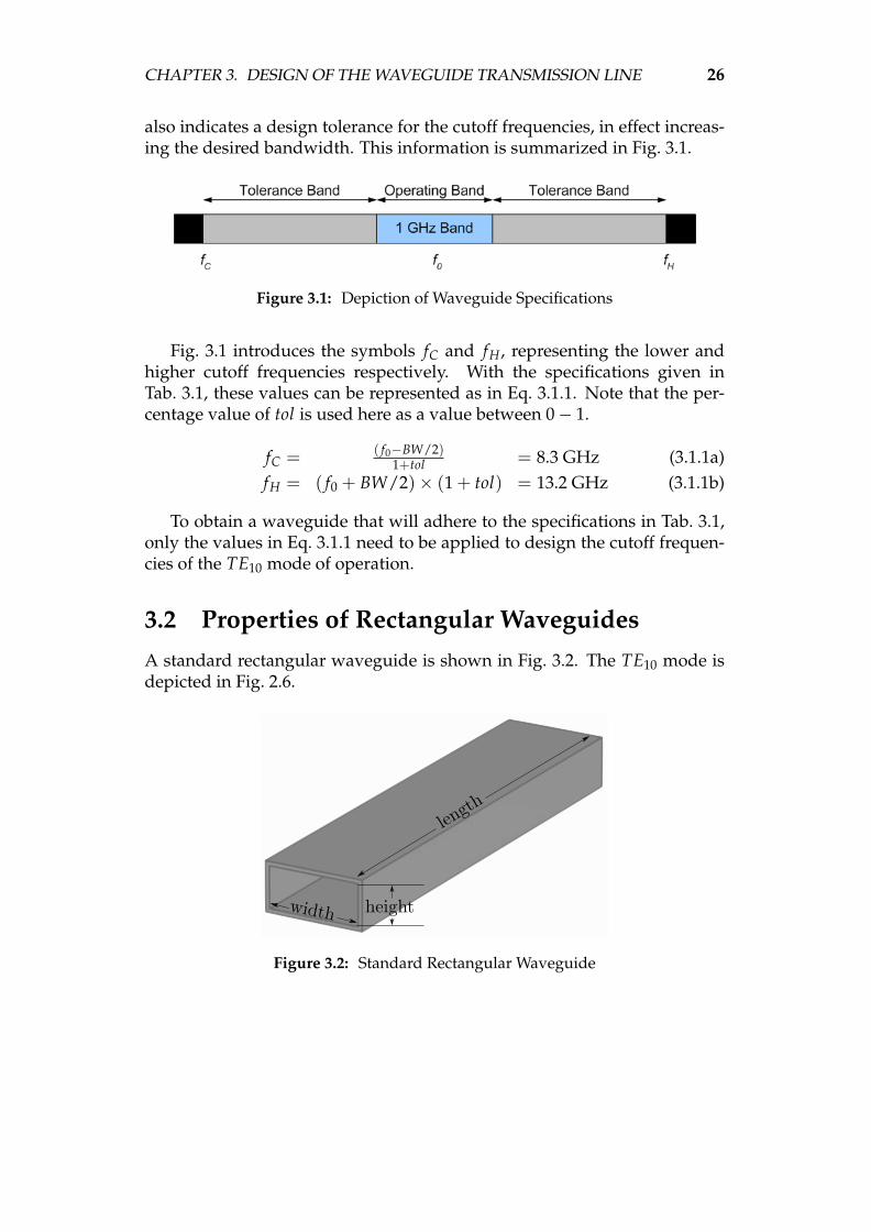
also indicates a design tolerance for the cutoff frequencies, in effect increas-ing the desired bandwidth. This information is summarized in Fig. 3.1.
Figure 3.1: Depiction of Waveguide Specifications
Fig. 3.1 introduces the symbols fC and fH, representing the lower andhigher cutoff frequencies respectively. With the specifications given inTab. 3.1, these values can be represented as in Eq. 3.1.1. Note that the per-centage value of tol is used here as a value between 0− 1.
fC = ( f0−BW/2)1+tol = 8.3 GHz (3.1.1a)
fH = ( f0 + BW/2)× (1 + tol) = 13.2 GHz (3.1.1b)
To obtain a waveguide that will adhere to the specifications in Tab. 3.1,only the values in Eq. 3.1.1 need to be applied to design the cutoff frequen-cies of the TE10 mode of operation.
3.2 Properties of Rectangular WaveguidesA standard rectangular waveguide is shown in Fig. 3.2. The TE10 mode isdepicted in Fig. 2.6.
Figure 3.2: Standard Rectangular Waveguide
CHAPTER 3. DESIGN OF THE WAVEGUIDE TRANSMISSION LINE 27
According to Microwave Encyclopedia [20], only two standard rectan-gular waveguide profiles will allow an operating frequency of f0 to propa-gate in the TE10 mode. Tab. 3.2 shows these two profiles and some of theirproperties. Both profiles were also simulated in CST Microwave Studio todetermine the actual cutoff values without any tolerances considered.
Table 3.2: Standard Rectangular Waveguide Profiles
Name Frequency Range [GHz] CST Range [GHz] Dimensions [mm]WR90 8.20 – 12.5 6.55 – 13.07 22.86× 10.16WR75 9.54 – 15.0 7.87 – 15.68 19.05× 9.525
It would be recommended to consider this profile for X-band applica-tions in the region near f0 due to its availability and cost. However, thespecifications in Tab. 3.1 state that the maximum width of the waveguideprofile must be 16 mm. The WR75 profile is too wide for this application,meaning that custom waveguides must be considered.
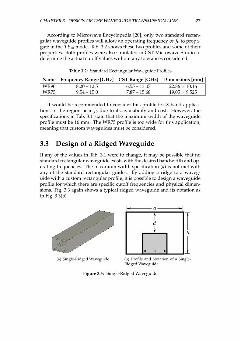
3.3 Design of a Ridged WaveguideIf any of the values in Tab. 3.1 were to change, it may be possible that nostandard rectangular waveguide exists with the desired bandwidth and op-erating frequencies. The maximum width specification (a) is not met withany of the standard rectangular guides. By adding a ridge to a waveg-uide with a custom rectangular profile, it is possible to design a waveguideprofile for which there are specific cutoff frequencies and physical dimen-sions. Fig. 3.3 again shows a typical ridged waveguide and its notation asin Fig. 3.3(b).
(a) Single-Ridged Waveguide (b) Profile and Notation of a Single-Ridged Waveguide
Figure 3.3: Single-Ridged Waveguide

CHAPTER 3. DESIGN OF THE WAVEGUIDE TRANSMISSION LINE 28
3.3.1 Approach to Understanding Ridged Waveguides
Take, as a starting point, the standard WR90 rectangular waveguide fromthe previous section. It has a simulated lower cutoff frequency of fC =6.55 GHz. This corresponds exactly to the predicted cutoff frequency im-plied by Eq. 2.1.15g, where the cutoff wavenumber can be interpreted asshown in Eq. 3.3.1.
kc = πa (3.3.1a)
and kc = 2πλc
(3.3.1b)
⇒ λc = 2πkc
∴ λc = 2a (3.3.1c)
The implication of Eq. 3.3.1c is that if the width of the waveguide is re-duced to conform to the physical specification in Tab. 3.1, the cutoff wave-length will be reduced and the cutoff frequency will increase. By adding aridge, the cutoff frequency can be lowered again as a result of the additionalcapacitance.
By sweeping the values d and s in Fig. 3.3(b), the cutoff frequency for thefirst and second cutoff frequencies can be determined and a suitable combi-nation can be chosen. The two dimensions that are swept in the simulationsare the width of the ridge (s) and the height of the ridge (b− d).
The first and second cutoff frequencies are stored and shown in Fig. 3.4.
3.3.2 Simulation Results for Parameter Sweep
A brute force numerical method is applied to obtain the physical dimen-sions that provides the desired performance required by the specificationsin Tab. 3.1. The inside width a must be no more than 16 mm. A value ofa = 14 mm is chosen, where b is kept the same as with the standard rect-angular profile WR90. In other words, the wide dimension of a rectangularwaveguide is shortened, raising the lower cutoff frequency. By adding aridge with the right dimensions, the cutoff frequencies can be tuned to thedesired specifications.
All values for the lower cutoff frequency below fC are acceptable and allvalues above fH is acceptable for the specifications given. It is necessary tofind the region where both these criteria are met. Fig. 3.5 shows this region.The red indicates all the combinations of values that will provide a ridgedwaveguide with the desired cutoff frequencies.

CHAPTER 3. DESIGN OF THE WAVEGUIDE TRANSMISSION LINE 29
02
46
8
0
5
105
6
7
8
9
10
11
HEIGHT
LOWER CUTOFF
WIDTH
CU
TO
FF
FR
EQ
UE
NC
Y T
HR
ES
HO
LD
(a) Lower Cutoff Frequencies
02
46
8
0
5
1011
12
13
14
15
16
HEIGHT
HIGHER CUTOFF
WIDTH
CU
TO
FF
FR
EQ
UE
NC
Y T
HR
ES
HO
LD
(b) Higher Cutoff Frequencies
Figure 3.4: Cutoff Frequencies of a Ridged Waveguide with a Fixed a and b

CHAPTER 3. DESIGN OF THE WAVEGUIDE TRANSMISSION LINE 30
Figure 3.5: Region Where Both the Lower and Higher Cutoff Frequency Specifica-tions are Met
3.3.3 Final Design of Ridged Waveguide
From the result in Fig. 3.5 it is clear that there are many solutions to thecorrect operating bandwidth of a ridged waveguide. To verify the validityof the design values of Fig. 3.5, a borderline case is taken and confirmedwith an individual simulation. A ridge height of (b − d) = 5 mm and aridge width of s = 6 mm is chosen as the confirmation values. The physicaldimensions of the waveguide profile are provided in Tab. 3.3 and Fig. 3.6.
Table 3.3: Properties of FinalRidged Waveguide Design
Property Valuea 14 mmb 10.16 mms 6 mmd 5.16 mm
(b− d) 5 mmfC 7.15 GHzfH 13.21 GHz
Figure 3.6: Physical Dimensionsof Final Ridged Waveguide
The dimensions chosen lies close to the border between the acceptableregion and the region where fH is too low in Fig. 3.5. This border is defined

CHAPTER 3. DESIGN OF THE WAVEGUIDE TRANSMISSION LINE 31
by the higher cutoff frequencies. In other words, the green region to the“right” of the acceptable region are for those values for which the secondcutoff frequency is lower than the desired cutoff value. It therefore makessense that the chosen fH is close to the design limit. The lower cutoff fre-quency fC, however, is well within its tolerance. This is because it is faraway from the blue region, where the lower cutoff frequency is higher thanfC. From the discussion of the waveguide wavelength (λg) and the conclu-sions drawn in Eq. 2.1.13b, it is can be seen that a lower cutoff frequencycorresponds to a shorter waveguide wavelength. This, in turn, serves toshorten the physical length of an array.
With the combination of the behavior of the surfaces given by Fig. 3.4(a)and Fig. 3.4(b) and the acceptability threshold provided by Fig. 3.5, manyphysical properties can be found that will generate a valid ridged waveg-uide. Similar curves can be made for any combination of a and b. All otherridged waveguides considered for the final application have the dimensionsgiven in Tab. 3.3.

Chapter 4
Analysis of Aperture Radiators
An exhaustive discussion of aperture radiators can easily distract from thefinal aim of finding a suitable element for the waveguide antenna array. Asubset of the more interesting properties are discussed and analyzed withrespect to several aperture antenna types. A common and well-understoodaperture antenna is discussed, as well as some arbitrary aperture configura-tions. The aim is to determine what slot to use in the final design, but alsoto verify the method used for analyzing the arbitrary aperture shapes.
4.1 Discussion of Slot Properties of InterestSection 2.2 provided a broad discussion on how aperture antennas are ex-cited, along with the equivalent circuit model and the notion of placementof apertures in a waveguide relating to its amplitude excitation. In all stud-ies, the waveguides are designed to make use of the TE10 mode.
It is generally understood that an aperture antenna’s radiating frequencycan be tuned by its length. The amplitude, depending on the shape of theaperture and configuration, can be tuned by rotating the aperture or bychanging the aperture’s offset from the center of the waveguide. For thesake of simplicity, it is assumed that the resonant frequency is the frequencywhere the maximum energy is being radiated. The amplitude is also as-sumed to be proportional to the radiated power.
In all studies, the resonant frequency is chosen to be f0 = 10.5 GHz; thesame as the design frequency for the final antenna. The effect of the aperturelength is ignored, but for the necessary tuning to ensure that all aperturesradiate at the same frequency. All antenna lengths are λ
2 k, where k ≈ 1 istuned until resonance is obtained.
The property that is used to control the amplitude differs, dependingon the type of aperture in question (hereafter referred to as the “amplitudetuner”). There are two classes, the offset aperture and the rotated apertures.The offset aperture is defined by the offset in the x-direction that the aper-
32

CHAPTER 4. ANALYSIS OF APERTURE RADIATORS 33
ture is placed from the centerline (the line along the z-axis) of the waveg-uide. Fig. 4.1 shows the axis and angle definitions required to interpret theamplitude tuners. The angle θ is used for rotated aperture antennas, wherethe offset is defined as the distance of the center of a slot in the x-direction.
Figure 4.1: Definition of Amplitude Tuners
Since low cross-polarization is one of the final goals of the research, it isalso a value that must be considered. For this application, vertical polariza-tion is desired, so the cross-polarization is the horizontal polarization. Herethe cross-polarization is treated as a ratio between the unwanted polariza-tion and the desired polarization, as shown in Eq. 4.1.1.
Cross-Polarization =Unwanted Polarization
Desired Polarization(4.1.1)
If these values are expressed in decibels (dB), which is a logarithmicscale, this ratio can be written as the difference between the two compo-nents as in Eq. 4.1.2.
Cross-Polarization [dB] = Unwanted Polarization [dB]−Desired Polarization [dB] (4.1.2)
Bandwidth is also be considered. Bandwidth here refers the 3dB-Powerbandwidth. In other words, the range of frequencies for which the aperturewill radiate more than or equal to half of the maximum radiated power. Thisvalue is expressed as a percentage of the center frequency ( f0). To obtain thevalue, Eq. 4.1.3 is used.
BW% =fMAX − fMIN
f0× 100 (4.1.3)
Define PMAX as the maximum radiated power, or the power at f0. The valuefMAX then refers to the first frequency f above f0 for which Pf = PMAX
2 ; fMIN

CHAPTER 4. ANALYSIS OF APERTURE RADIATORS 34
refers to the first frequency below f0 for which this is true. The results forthese parameters are given and discussed in section 4.9.
4.2 Study: Offset Rectangular Aperture in theBroadwall
A rectangular aperture, cut into the broadwall of a rectangular waveguideand offset from the centerline, is shown by Fig. 4.2.
(a) 3D Wireframe of Aperture (b) Top View of Aperture in Waveguide
Figure 4.2: Model for Rectangular Aperture at Some Offset from the Center-line ofthe Waveguide
The waveguide used here is the standard WR90 rectangular waveguideused for many X-band applications. Its dimensions are 22.86 × 10.16mmand is used here for all studies that require a rectangular waveguide profile.
By sweeping the value of the offset, the offset of the rectangular aperture,the power that is radiated can be increased. The length of the aperture istuned for each of these offsets until the maximum power is radiated at thecenter frequency.
The Amplitude Tuner axis in the figures in section 4.9 refers, in this case,to the possible range of offsets for the aperture. The lower percentage valuerefers to the offset that corresponds to the lower radiated power and thehigher percentage refers to the largest offset. For example, a value of 50%refers to the aperture being placed halfway between the centerline and thewall of the waveguide.
4.2.1 Bandwidth
Fig. 4.11 shows how the bandwidth changes with the amplitude. The val-ues range from 10%− 14% for the offset rectangular aperture. These valuesare used as the benchmark against which the other studies are compared.

CHAPTER 4. ANALYSIS OF APERTURE RADIATORS 35
Rectangular apertures have been used for many years in a variety of appli-cations, indicating that their performance characteristics are sufficient forpractical applications.
4.2.2 Amplitude
The amplitude of the rectangular aperture is depicted in Fig. 4.12. It canbe seen that a given aperture can radiate between 0% − 40% of the inputpower, depending on its offset. This behavior corresponds to the expectedbahavior of an offset aperture placed in the broadwall of a waveguide prop-agating the TE10 mode. As the offset increases, the aperture cuts more sur-face current, increasing the strength of the electric field that forms across thegap.
4.2.3 Cross-Polarization
This study is the only one for which the cross-polarization decreases withradiated power, as can be seen in Fig. 4.13. In other words, for high-powerelements, the offset aperture will provide lower cross-polarization levelsthan the other configurations considered here. However, for lower values(less than 5% of the input power radiated by the aperture as is typical forlarge arrays), it may be better to use a different type of aperture.
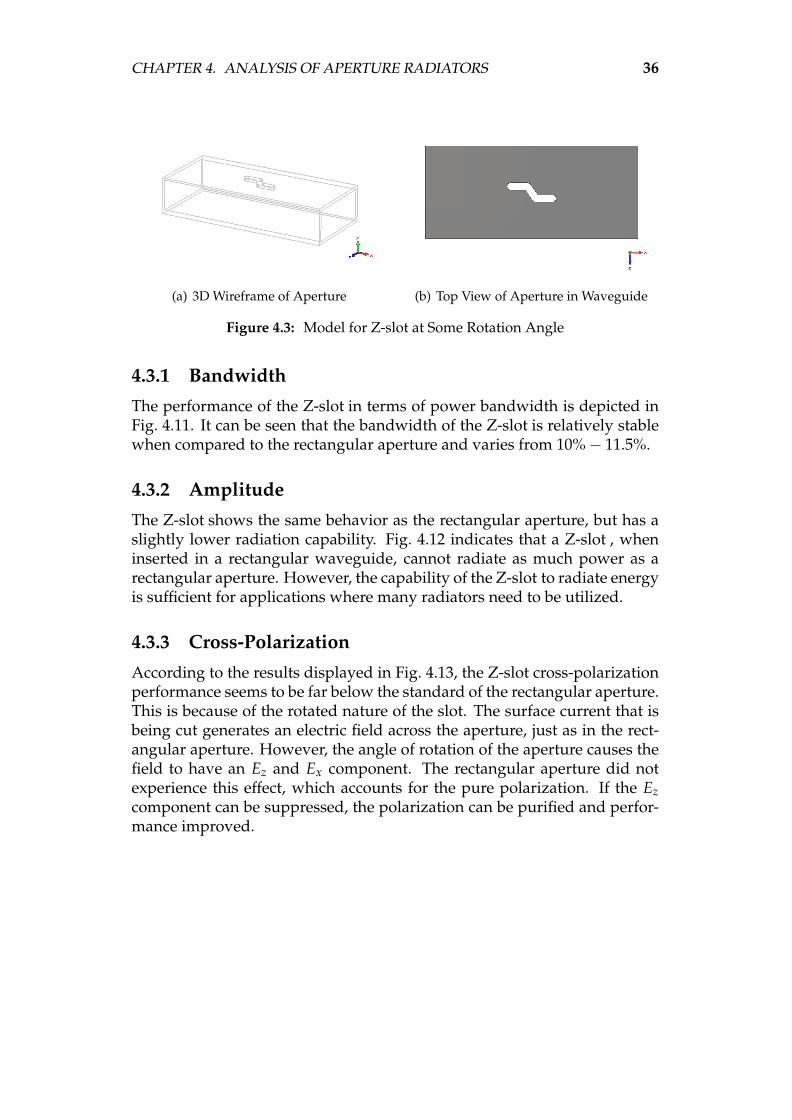
4.3 Study: Z-slot Aperture in the BroadwallFig. 4.3 depicts a Z-slot cut into a standard rectangular waveguide. TheZ-slot , named for its shape, is an aperture that is a combination of a rotatedrectangular aperture and an offset aperture (see Fig. 2.10 for a depictionof these two configurations). The radiated power is altered by rotating thefixed length center section of the “Z”, while the two horizontal tabs are usedfor tuning the center frequency.
The Amplitude Tuner axis for the rotated slots refers to the rotation an-gle. The rotation θ may vary from 0 − 90, where θ = 90 is the same asa rectangular aperture placed in the center of the waveguide. The roundededges of the Z-slot is to model the aperture as it would be used in practiceif machining techniques are used during manufacture. This is not done forthe rectangular slots, as they are only for theoretical comparison and the lit-erature generally does not take the rounding of corners into account. Whenreading the data in Fig. 4.11-4.13, note that θ = 90 corresponds to the lowerexcitation limit of 0% and θ = 0 corresponds to 100%.
CHAPTER 4. ANALYSIS OF APERTURE RADIATORS 36
(a) 3D Wireframe of Aperture (b) Top View of Aperture in Waveguide
Figure 4.3: Model for Z-slot at Some Rotation Angle
4.3.1 Bandwidth
The performance of the Z-slot in terms of power bandwidth is depicted inFig. 4.11. It can be seen that the bandwidth of the Z-slot is relatively stablewhen compared to the rectangular aperture and varies from 10%− 11.5%.
4.3.2 Amplitude
The Z-slot shows the same behavior as the rectangular aperture, but has aslightly lower radiation capability. Fig. 4.12 indicates that a Z-slot , wheninserted in a rectangular waveguide, cannot radiate as much power as arectangular aperture. However, the capability of the Z-slot to radiate energyis sufficient for applications where many radiators need to be utilized.
4.3.3 Cross-Polarization
According to the results displayed in Fig. 4.13, the Z-slot cross-polarizationperformance seems to be far below the standard of the rectangular aperture.This is because of the rotated nature of the slot. The surface current that isbeing cut generates an electric field across the aperture, just as in the rect-angular aperture. However, the angle of rotation of the aperture causes thefield to have an Ez and Ex component. The rectangular aperture did notexperience this effect, which accounts for the pure polarization. If the Ezcomponent can be suppressed, the polarization can be purified and perfor-mance improved.

CHAPTER 4. ANALYSIS OF APERTURE RADIATORS 37
4.4 Study: Z-slot Aperture in the Broadwall withPolarizer Plates
The previous section indicated that the rotated nature of the Z-slot causesan extra field component (Ez) to be generated, which is the field that con-tributes to the cross-polarization. In an effort to suppress this component,two plates are placed on either side of the aperture as depicted in Fig. 4.4.
Section 2.1.2 shows that two parallel plates of conducting material canbe treated as a transmission line. The equations in Eq. 2.1.8 are valid ifthe parallel plates are fed with a field sufficient to excite the TE1 mode.That is, an electric field tangential to the direction of propagation must beprovided at a sufficient frequency. The field must also be oriented such thatthe field points from one plate to the other (the Ey component in Fig. 2.2).It is important to note that the other field components (e.g. Ex and Ez) aresuppressed. This implies that if the plates are fed with a field that has twotangential components in the electric field, that only one will be propagated.
(a) 3D Wireframe of Aperture (b) Top View of Aperture in Waveguide
Figure 4.4: Model for Z-slot with 10mm Polarizer Plates
4.4.1 Bandwidth
Despite the anomalous behavior of the percentage bandwidth at lower ex-citations, it appears as though the trend for a Z-slot with polarizer platesis that the bandwidth decreases with excitation. The values vary between9.5%− 12% bandwidth.
4.4.2 Amplitude
The polarizing plates seem to have little effect on the radiation capabil-ity of the Z-slot . At low excitations in particular, Fig. 4.12 shows thata Z-slot inserted into a rectangular waveguide radiates almost the same

CHAPTER 4. ANALYSIS OF APERTURE RADIATORS 38
amount of energy, despite the presence of the plates. Neither the Z-slot byitself, nor the Z-slot with the polarizer plates can achieve the same radiationcapability as the rectangular aperture.
4.4.3 Cross-Polarization
For the polarizer plates to prove useful, the cross-polarization performanceis critical. The addition of two 10 mm long plates suppress the cross-polarization level by as much as 20 dB. This improvement places theZ-slot performance in the same order as the rectangular aperture, partic-ularly at lower excitations.
4.5 Study: Z-slot Aperture in a RidgedWaveguide
It has been shown that the Z-slot can provide performance comparable tothat of a rectangular aperture antenna in terms of bandwidth, radiation ca-pability and cross-polarization, provided that parallel plates are used tosuppress the unwanted polarization. However, as discussed in chapter 3,it is sometimes desirable to use a waveguide with a different profile.
It is important to confirm that the performance of the apertures are notaffected too greatly by the change in the waveguide. Fig. 4.5 depicts aZ-slot inserted into the waveguide that is used in the design of chapter 6.
(a) 3D Wireframe of Aperture (b) Top View of Aperture in Waveguide
Figure 4.5: Model for Z-slot in a Ridged Waveguide

CHAPTER 4. ANALYSIS OF APERTURE RADIATORS 39
4.5.1 Bandwidth
The bandwidth of a Z-slot when inserted into the ridged waveguide ofFig. 4.5 is shown in Fig. 4.11. Of the studies conducted here, it providesthe highest bandwidth for any given excitation.
4.5.2 Amplitude
The change in waveguide profile has changed the radiation capability ofthe Z-slot in such a way that the amplitudes are comparable to that of therectangular aperture. A given Z-slot , inserted into a rectangular waveg-uide, radiates only about 70% of the power than if it is inserted in a ridgedwaveguide. This behavior can be ascribed to the higher field concentrations(i.e. the stronger surface currents) at the surface where the slot is inserted.
4.5.3 Cross-Polarization
Fig. 4.13 shows that the Z-slot in a ridged waveguide has almost identicalproperties to that of a Z-slot in a rectangular waveguide. However, there isan offset of 2–5 dB, indicating that the initial component of the undesiredpolarization is stronger when the aperture is excited in a ridged guide thanif it is excited in a rectangular guide.
4.6 Study: Z-slot Aperture in a RidgedWaveguide with Polarizer Plates
The aperture configuration that is used in the final design is depicted inFig. 4.6. Fig. 4.6(a) shows how the ridged waveguide profile, polarizerplates and Z-slot are combined to provide a solution whose physical andperformance properties adheres to the desired specification.
4.6.1 Bandwidth
The bandwidth of the Z-slot with polarizer plates in a ridged waveguideperforms sufficiently well compared to other apertures and configurations.Depending on the excitation, the bandwidth varies between 11% − 12%,which is the most stable bandwidth of the configurations studied.
4.6.2 Amplitude
Fig. 4.12 shows that the excitation range is the highest of the configurationspresented here, with a range of up to 42% of the input power radiated by asingle element. It is unlikely that such values will be needed for an array,

CHAPTER 4. ANALYSIS OF APERTURE RADIATORS 40
(a) 3D Wireframe of Aperture (b) Top View of Aperture in Waveguide
Figure 4.6: Model for Z-slot with 10mm Polarizer Plates in a Ridged Waveguide
but this range does indicate the sensitivity of the aperture to its rotationangle. Higher sensitivity implies that finer manufacturing tolerances arerequired, but also that a smaller range of tuning values are required. Sincethe Z-slot appears to have lower cross-polarization levels at lower tuningvalues, this could be advantageous.
4.6.3 Cross-Polarization
Again, the cross-polarization of the Z-slot in a ridged waveguide tracks thecounterpart in a rectangular waveguide reasonably well, even with the po-larizer plates present. Fig. 4.13 again depicts an offset of 2–5 dB as seenwith the same configuration without the plates. If the range of apertures forthe final design requires elements to radiate up to 15% of the input power,then the range of cross-polarization levels is the same as for the rectangularaperture, namely < −35 dB.
4.7 Study: Varying Polarizer Plate Lengths in aZ-slot Ridged Waveguide Configuration
In both the studies involving the Z-slot , the presence of a 10 mm lengthpolarizer plate suppressed the cross-polarization of the configuration by 20–25 dB. The bandwidth and radiation capacity of the slots were reasonablyunaffected, making polarizer plates a viable option for cross-polarizationsuppression.
This study varies the length of the polarizer plates surrounding aZ-slot antenna inserted in a ridged waveguide as in Fig. 4.6. A polarizer ofzero length reduces to the model in Fig. 4.5. A slot angle of θ = 25 is chosenand as the model is changed, the length is tuned to ensure resonance. The

CHAPTER 4. ANALYSIS OF APERTURE RADIATORS 41
length of the polarizer is swept between 1–15 mm and the cross-polarizationlevel is studied.
0 5 10 15−40
−35
−30
−25
−20
−15
−10
−5
Polarizer Plate Length [mm]
Cro
ss−
Pol
ariz
atio
n Le
vel [
dB]
Cross−Polarization vs. Polarizer Length
Baselinewith Polarizer
Figure 4.7: Cross-Polarization Level with Varying Polarizer Plate Lengths
Fig. 4.7 shows the cross-polarization of the configuration as the polar-izer plate length is increased. The blue line at −6.63 dB shows the inherentcross-polarization of the configuration in the absence of polarizer plates. Itcan be seen that in general, a longer length of polarizer plate will providemore suppression of the unwanted polarization. The previous studies haveshown that even though there is a strong link between the polarizer platesand the cross-polarization suppression, the bandwidth and radiated poweris also affected.
Fig. 4.8 shows the bandwidth properties of the configuration when thelengths of the plates are varied. The blue line at 14.5 % is again the baselinebandwidth in the absence of polarizer plates. The bandwidth can be pushedup to double the baseline value with the proper selection of plate length.Since bandwidth is related to the quality factor Q of the antenna, it may beuseful to look at the variation of this property as well. The bandwidth isrelated to Q by Eq. 4.7.1 [5].
Q = ωaverage energy stored
energy loss/second=
100BW%
(4.7.1)
The stored energy can be stored as both magnetic (Wm) and electric (We)energy. Resonance, by definition, is that frequency where these two valuesare equal (W = Wm = We) [5]. The quality factor can then also be written as

CHAPTER 4. ANALYSIS OF APERTURE RADIATORS 42
0 5 10 1510
12
14
16
18
20
22
24
26
28
Polarizer Plate Length [mm]
3dB
Ban
dwid
th [%
]
3dB Bandwidth vs. Polarizer Length
Baselinewith Polarizer
Figure 4.8: Bandwidth Variation as a Result of Varying Polarizer Plate Lengths
in Eq. 4.7.2a. Fig. 4.9 shows both the quality factor and the radiated powerfor comparison.
Q = 2π f0Wm+We
PR= 2π f0
2WPR
(4.7.2a)
⇒ W = QPR4π f0
(4.7.2b)
From Eq. 4.7.2b it can be shown that if the radiated power as well as thequality factor decreases, that the stored energy must decrease as well. Thismeans that even though it is possible to obtain a higher radiation capabilityfrom an aperture, it will also store more energy in the electric and magneticfields of the configuration. It is suspected that mutual coupling betweenelements is related to the stored fields, making this an undesirable result.As a compromise, it is recommended that the polarizer length should bechosen based on two criteria:
1. the level of desired cross-polarization suppression; and
2. the length of polarizer plate that will leave other performance proper-ties reasonably unaffected.
The properties of the configuration with a polarizer plate length of10 mm that is used in other studies, can be compared to the baseline val-ues as shown in Tab. 4.1.
Tab. 4.1 shows that with proper selection of the polarizer plate length, itis possible to obtain Z-slot elements that can radiate the same power over

CHAPTER 4. ANALYSIS OF APERTURE RADIATORS 43
0 5 10 1520
22
24
26
28
30
32
34
36
38
40
Polarizer Plate Length [mm]
Rad
iate
d P
ower
[%]
Radiated Power vs. Polarizer Length
Baselinewith Polarizer
(a) Percentage of Power Radiated at f0 for Varying Polarizer Plate Lengths
0 5 10 153
4
5
6
7
8
9
10
Polarizer Plate Length [mm]
Q−
Fac
tor
Q−Factor vs. Polarizer Length
Baselinewith Polarizer
(b) Quality Factor at f0 for Varying Polarizer Plate Lengths
Figure 4.9: Radiated Power and Q-Factor for Varying Polarizer Plate Lengths
the same bandwidth as when the polarizer plates are absent. The reasonfor doing this is to achieve the cross-polarization suppression evident fromFig. 4.7. Tab. 4.1 shows a suppression of −23.6 dB in the cross-polarizationfor this element whilst leaving other properties relatively unaffected.

CHAPTER 4. ANALYSIS OF APERTURE RADIATORS 44
Table 4.1: Properties of a 25 Z-slot Antenna Compared to the Addition of Polar-izer Plates
Property Baseline 10 mm PlatesCross-Polarization Level -6.63 dB -30.22
Radiation Capacity 32.69% 35.18%3dB Bandwidth Percentage 14.53% 12.1%
Q-Factor 6.881 8.264
4.8 Equivalent Circuit ModelsSection 2.2.2 stated that the equivalent model of an aperture may be ap-proximated as either that of a series impedance or a parallel admittance.Fig. 4.10 shows the phase of S11 for both the offset rectangular aperture andthe Z-slot aperture.
9 9.5 10 10.5 11 11.5 12-200
-150
-100
-50
0
50
100
150
200
Frequency [GHz]
Pha
se [d
eg]
Phase of S11
Offset Rect.Z-Slot
Figure 4.10: Phase of S11 for an Offset Aperture and a Z-slot
The difference in determining resonance stems from where the reflectedvoltage waves come from. The offset aperture responds similarly to that ofa parallel impedance as depicted in Fig. 2.10(a). The Z-slot responds morelike a series impedance as depicted in Fig. 2.10(b). However, the responseof the Z-slot appears to be more complex. It may be necessary to use themore complete Π or T model networks to characterize the Z-slot . For thepurposes of the work done here, the series impedance model is sufficient.

CHAPTER 4. ANALYSIS OF APERTURE RADIATORS 45
4.9 Simulation ResultsThe results of several studies discussed in this chapter are given here forconvenience in Fig. 4.11 – 4.13. Each study discusses the data in Fig. 4.11 –4.13 as it pertains to that study.
0 20 40 60 80 1007
8
9
10
11
12
13
14
15
Amplitude Tuner [% of Possible Range]
3dB
Ban
dwid
th [%
]
3dB Bandwidth vs. Amplitude Tuner
BroadWall RectZ−SlotZ−Slot PolZ in RidgedWGZPol in RidgedWG
Figure 4.11: Percentage Bandwidth

CHAPTER 4. ANALYSIS OF APERTURE RADIATORS 46
0 20 40 60 80 1000
5
10
15
20
25
30
35
40
45
Amplitude Tuner [% of Possible Range]
Max
imum
Rad
iate
d P
ower
[%]
Maximum Radiated Power vs. Amplitude Tuner
BroadWall RectZ−SlotZ−Slot PolZ in RidgedWGZPol in RidgedWG
Figure 4.12: Percentage of Power Radiated by Aperture
0 20 40 60 80 100−70
−60
−50
−40
−30
−20
−10
0
Amplitude Tuner [% of Possible Range]
Cro
ss−
Pol
ariz
atio
n Le
vel [
dB]
Cross−Polarization vs. Amplitude Tuner
BroadWall RectZ−SlotZ−Slot PolZ in RidgedWGZPol in RidgedWG
Figure 4.13: dB Cross-Polarization Level
Chapter 5
Algorithms for ApertureCharacterization & AntennaOptimization
5.1 Discussion of the Parameter SweepAlgorithm
The flow chart for the algorithm of the parameter sweep is given in Fig. 5.1.Its structure is simple in that there are few branches and decisions that mustbe made. Before the algorithm can be executed, a CST model must be cre-ated with the aperture configuration that will be used in the array design.Three apertures are placed adjacent to one another to simulate a more real-istic operating environment.
Fig. 5.2(a) shows the environment used to characterize a Z-slot . Thecenter Z-slot ’s impedance is the one that is calculated from the scatteringparameters. Matlab modifies the CST model to have the physical valuesrequired for an iteration of the loop shown in Fig. 5.1. The results are thenpulled back into Matlab for further processing.
Once the entire range is simulated, a rough estimation of the behaviorof the aperture is known. The resolution is then artificially enhanced byinterpolating between the points. A high resolution will give a better firstorder estimate of any desired value. These higher resolution surfaces for thereal, imaginary and bandwidth properties of the apertures are then storedfor the optimization algorithm to implement an array design.
47

CHAPTER 5. ALGORITHMS FOR APERTURE CHARACTERIZATION &ANTENNA OPTIMIZATION 48
Initialize variables and
determine the ranges of the
values to sweep
Has the whole
range been run?
Run the new simulation with
new physical aperture
dimensions
No
Extract Real, Imaginary and
Bandwidth impedance
information for this aperture
Interpolate surfaces to
artificially increase
resolution
Yes
Store the surfaces for the
Real, Imaginary and
Bandwidth information of
the slot, along with the
range of physical values
Parameter Sweep
Figure 5.1: Flow Chart of the Parameter Sweep

CHAPTER 5. ALGORITHMS FOR APERTURE CHARACTERIZATION &ANTENNA OPTIMIZATION 49
(a) Z-slot Calibration Model for the Parameter Sweep
(b) Port Locations Between Apertures and their Normal Directions
Figure 5.2: Z-slot Environment and Port Definitions
5.2 Extraction of Impedance Properties fromS-Parameters
The extraction of the real, imaginary and bandwidth properties is non-trivial and requires further discussion. The S-parameter is defined as theratio between the reflected voltage wave measured at a port “i” vs. the in-put voltage wave at port “j”. The notation for this ratio is given in Eq. 5.2.1.
Sij =bi
aj
∣∣∣∣∣V+
k =0 for k 6=j
(5.2.1)
In Eq. 5.2.1, aj is the incident voltage wave at port “j” and bi is the re-flected voltage wave (at port i = j) or the transmitted voltage wave (at porti 6= j) [5]. Note that the definition allows only one port to be active at a time.Using this convention, the scattering matrix for the model in Fig. 5.2(b) iswritten in Eq. 5.2.2.

CHAPTER 5. ALGORITHMS FOR APERTURE CHARACTERIZATION &ANTENNA OPTIMIZATION 50
b1b2b3b4b5b6
=
s11 s12 s13 s14 s15 s16s21 s22 s23 s24 s25 s26s31 s32 s33 s34 s35 s36s41 s42 s43 s44 s45 s46s51 s52 s53 s54 s55 s56s61 s62 s63 s64 s65 s66
a1a2a3a4a5a6
(5.2.2a)
B = SA (5.2.2b)
For a traveling wave antenna, energy is inserted into the waveguide atone end and propagates through the waveguide until it meets a terminatingload. In other words, energy is coming from one end and is dissipated alongthe line. The load at the end absorbs the last of the energy from which noth-ing is reflected. When this principle is translated to the model in Fig. 5.2(b),energy is inserted into the guide at port 1. Port 2 absorbs all of the energythat is not radiated by the aperture. The energy that flows out of port 3 isexactly equal to the energy absorbed by port 2. In the same way the energycan be tracked up to port 6, where the last of the energy is absorbed. Thiscan be written in vector form as in Eq. 5.2.3.
B =
b1b2b3b4b5b6
; A =
1∠0
b3b2b5b40
(5.2.3)
In other words, the excitation vector can be written in terms of the in-cident and reflected waves. This means that, since S is known from CSTsimulations, six independent equations can be written with four unknownsto solve (i.e. b2...b4). When A is substituted back into Eq. 5.2.2 and multi-plied out, equations for each of the reflected voltage waves are obtained inthe form of Eq. 5.2.4.
b2 = s211∠0 + s22b3 + s23b2 + s24b5 + s25b4... =
... (5.2.4)b5 = s511∠0 + s52b3 + s53b2 + s54b5 + s55b4
Placing Eq. 5.2.4 back into vector form and further simplified to a newmatrix form as in Eq. 5.2.5.

CHAPTER 5. ALGORITHMS FOR APERTURE CHARACTERIZATION &ANTENNA OPTIMIZATION 51
s21 =[
(1− s23) −s22 −s25 −s24]
B... =
... (5.2.5a)s51 =
[−s53 −s52 −s55 (1− s54)
]B
s21s31s41s51
=
(1− s23) −s22 −s25 −s24−s33 (1− s32) −s35 −s34−s43 −s42 (1− s45) −s44−s53 −s52 −s55 (1− s54)
b2b3b4b5
(5.2.5b)
C = QBsub (5.2.5c)
The constants vector is represented by C, Q is a subset matrix of the S-parameters and Bsub is a subset vector of B. At closer inspection, it can beseen that Q can also be written as in Eq. 5.2.5d.
Q =
1 0 0 00 1 0 00 0 1 00 0 0 1
−
s23 s22 s25 s24s33 s32 s35 s34s43 s42 s45 s44s53 s52 s55 s54
(5.2.5d)
To solve for Bsub, some manipulation can be performed to obtain thematrix solution given in Eq. 5.2.6.
C = QBsub
Q−1C = Q−1QBsub
Bsub = Q−1C. (5.2.6)
The relationship between the reflected voltages and excitation voltagesgiven in Eq. 5.2.3. Reflection coefficients can now be calculated at any port,since all of the excitation and reflected voltages are known. The reflectioncoefficient for port 3, for example, can now be written as in Eq. 5.2.7.
Γ3 =b3
a3=
b3
b2(5.2.7)
Remember that there is a phase shift (call it ∆φ) associated with energythat propagates down a length of transmission line. Eq. 5.2.7 represents thereflection coefficient at the location of port 3. To move the reference pointto the center of the slot, this phase shift must be taken into account for boththe time it takes the incident wave to hit the aperture as well as the return

CHAPTER 5. ALGORITHMS FOR APERTURE CHARACTERIZATION &ANTENNA OPTIMIZATION 52
time. This is shown in Eq. 5.2.8.
ΓA = b3e−j∆φ
b2e+j∆φ
= b3b2× e−2j∆φ (5.2.8a)
To convert from this reflection coefficient to the load impedance, Eq 5.2.9is applied [5]. This now includes the impedance of the slot as well as theterminating load impedance (i.e. the input impedance behind the aperture).Note that Z0 = 1 for the normalized system being used.
ZIN = Z01 + ΓA
1− ΓA=
1 + ΓA
1− ΓA(5.2.9)
Again, ZIN refers to the input impedance that includes both the apertureand the input impedance after the aperture. Since only the impedance ofthe aperture is of interest, it is necessary to calculate the input impedance atport 5 in the same way. This time the transmission line phase shift must becalculated to the other direction as shown in Eq. 5.2.10.
Γ5 =b4
b5× e2j∆φ (5.2.10)
Apply Eq. 5.2.9 to this reflection coefficient as in Eq. 5.2.11 and calculatethe load impedance ZL.
ZL =1 + Γ5
1− Γ5(5.2.11)
The aperture impedance can be calculated by subtracting the two values,as they are placed in series (call it ZS). If the element were to be a parallelimpedance (call it ZP), all of the calculations would be identical, except thatthe aperture would be taken as a parallel impedance to the load impedance.The calculation of the aperture impedance is given in Eq. 5.2.12, where theequivalent model of the aperture would determine whether ZS (Fig. 5.3(a))or ZP (Fig. 5.3(b)) is used.
ZS = ZIN − ZL (5.2.12a)ZP = ZIN ZL
ZL−ZIN(5.2.12b)
Any aperture that can be modeled as a series or parallel impedance canbe calculated in this way. This method is used to gain an initial estimate ofaperture impedance for all of the following designs.

CHAPTER 5. ALGORITHMS FOR APERTURE CHARACTERIZATION &ANTENNA OPTIMIZATION 53
Figure 5.3: Location of Aperture Impedances With Respect to the Load Impedance
5.3 Simulation Results of a Parameter SweepThe purpose of the parameter sweep is to characterize an aperture antennain an environment similar to the one in which it will be implemented. Thatwhich is needed for this characterization includes information on the realpart of the impedance, the imaginary part of the impedance and an indica-tion of how quickly the values change. This information enables a reason-able first order estimate of the individual aperture properties of an array.This information is presented in the surfaces of Fig. 5.4–5.6.
Figure 5.4: Resistance: Real Part of the Aperture Impedance

CHAPTER 5. ALGORITHMS FOR APERTURE CHARACTERIZATION &ANTENNA OPTIMIZATION 54
Figure 5.5: Reactance: Imaginary Part of the Aperture Impedance
The grids are obtained by calculating the impedance of a number of CSTsimulations with varying slot lengths and angles. Every frequency has itsown impedance, so the values of Z at f0 are isolated and plotted in Fig. 5.4–5.5 in its real and imaginary components. The values are then interpolatedto artificially increase the resolution.
The phase slope is defined by locating the resonant frequency for anycalculated impedance. This would be the frequency where the imaginarycomponent is zero, or alternatively where the phase of the impedance iszero. If the change in phase is assumed to be linear in the region near theresonant frequency, a slope can be calculated that will indicate how quicklythe aperture moves away from the resonant frequency. The slope is takenbetween −5 to 5 as depicted in Fig. 5.7.
Only the grids in Fig. 5.4–5.5 are used for the first-order design. Ev-ery point on the slot length and angle axes provides a data point for thereal and imaginary components of the impedance. In other words, for anycombination of physical parameters, there is an associated impedance. Theimpedances of interest are those for which the imaginary component is zero.When the curve from Fig. 5.5 that corresponds to Im(Z) = 0 is traced ontothe surface of Fig. 5.4, a single curve in 3D space is obtained that gives thepurely real aperture impedances.

CHAPTER 5. ALGORITHMS FOR APERTURE CHARACTERIZATION &ANTENNA OPTIMIZATION 55
Figure 5.6: Phase Slope: Rate with which Impedance Changes
Figure 5.7: Phase of the Impedance

CHAPTER 5. ALGORITHMS FOR APERTURE CHARACTERIZATION &ANTENNA OPTIMIZATION 56
5.4 Optimization AlgorithmThe term optimization is used here informally to describe the process of ob-taining the best result for a design through the systematic application of aset of rules. The process is depicted in the flow chart in Fig. 5.8. The algo-rithm adjusts certain design parameters with each iteration with the aim ofimproving the performance characteristics of the antenna. The cycle termi-nates when the antenna shows the desired performance characteristics.
Figure 5.8: Flow Chart of the Optimization Algorithm
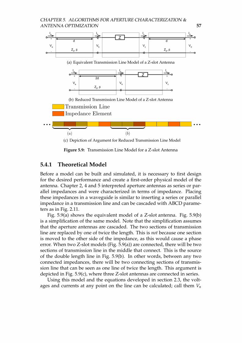
CHAPTER 5. ALGORITHMS FOR APERTURE CHARACTERIZATION &ANTENNA OPTIMIZATION 57
(a) Equivalent Transmission Line Model of a Z-slot Antenna
(b) Reduced Transmission Line Model of a Z-slot Antenna
(c) Depiction of Argument for Reduced Transmission Line Model
Figure 5.9: Transmission Line Model for a Z-slot Antenna
5.4.1 Theoretical Model
Before a model can be built and simulated, it is necessary to first designfor the desired performance and create a first-order physical model of theantenna. Chapter 2, 4 and 5 interpreted aperture antennas as series or par-allel impedances and were characterized in terms of impedance. Placingthese impedances in a waveguide is similar to inserting a series or parallelimpedance in a transmission line and can be cascaded with ABCD parame-ters as in Fig. 2.11.
Fig. 5.9(a) shows the equivalent model of a Z-slot antenna. Fig. 5.9(b)is a simplification of the same model. Note that the simplification assumesthat the aperture antennas are cascaded. The two sections of transmissionline are replaced by one of twice the length. This is not because one sectionis moved to the other side of the impedance, as this would cause a phaseerror. When two Z-slot models (Fig. 5.9(a)) are connected, there will be twosections of transmission line in the middle that connect. This is the sourceof the double length line in Fig. 5.9(b). In other words, between any twoconnected impedances, there will be two connecting sections of transmis-sion line that can be seen as one line of twice the length. This argument isdepicted in Fig. 5.9(c), where three Z-slot antennas are connected in series.
Using this model and the equations developed in section 2.3, the volt-ages and currents at any point on the line can be calculated; call them Vn

CHAPTER 5. ALGORITHMS FOR APERTURE CHARACTERIZATION &ANTENNA OPTIMIZATION 58
and In respectively. Since only the voltages and currents at the aperturesare of interest, Vn and In will only be used to refer to the voltages and cur-rents over the impedances, meaning that n is a number between 1 and thenumber of elements in the array.
The array synthesis requires a specific voltage or current weighting overa radiating element, depending on the equivalent circuit model of the aper-ture. The Villeneuve power distribution is shown in Fig. 5.10, along withthe impedance distribution that will provide the power distribution.
0 5 10 15 200
5
10
Pow
er D
istr
ibut
ion
[%]
Element Number
Designed Power and Impedance Distributions
0 5 10 15 200
0.2
0.4
Impe
danc
e |Z
|
Figure 5.10: Villeneuve Power and Impedance Distribution
Each element in the array has a certain impedance associated with it.The mismatch caused by each cascaded element cause reflections back tothe source. If all of these reflections add in phase, it disrupts the assumedone-way flow of power down the transmission line. To counter this effectin traveling-wave applications, the element spacing is altered such that thereflections add out of phase, thus diminishing the effect of reflections.
The transmission line model is again used to determine the total inputreflection of the array. If the return loss, given by Eq. 5.4.1, is more than adesigned threshold, the spacing is changed and the loss is calculated again.The smallest element spacing (i.e. the phase difference between the elementexcitation) that adheres to the desired return loss threshold is used.
RL = −20 log |Γ| (5.4.1)
Note that the only design criteria are the power distribution and the re-turn loss. The impedances are calculated from the transmission line model

CHAPTER 5. ALGORITHMS FOR APERTURE CHARACTERIZATION &ANTENNA OPTIMIZATION 59
based on the desired power radiation of each element and the return lossdetermines the element spacing.
Once the impedances are known that will provide the necessary powerdistribution, the values can be looked up from the grids generated by theaperture characterization in chapter 5.
The physical parameters that are read from the grids, along with the cal-culated element spacing, is now used to generate a CST model. The model issimulated and the farfields and electric fields are stored. The electric field’samplitude and phase relate strongly to the excitation of an aperture. Re-gardless of the equivalent model of the aperture, the radiation occurs froman electric field forming over the gap of the aperture. By looking at the E-field some distance (> λ0
2 ) from the aperture, the excitation of the aperturecan be determined. The E-field represents either the voltage over a serieselement, or the current through a parallel impedance. An example of sucha field is depicted in Fig. 5.11(a).
A windowing is performed where the average field over the region ofeach element is taken as the element weighting. The values are normalized,so the exact value is not important, only the pattern. For the phase shownin Fig. 5.11(b), only the value directly above the center of the element istaken. The distribution in Fig. 5.11(a) must be the square root of the powerdistribution (in order to obtain the excitation) given in Fig. 5.10 and thephase must change linearly due to the non-resonant element spacing.
5.4.2 Interpretation of Simulation Results
The power that is not radiated by the antenna or reflected back to the source,must be the power absorbed by the load (PL). This can be calculated asin Eq. 5.4.2a. Similarly, the total radiated power (PR) must be the inputpower minus the power absorbed by the terminating load and the inputport. Eq. 5.4.2b gives this equation in terms of S-parameters.
PL = S221 (5.4.2a)
PR = 1− S211 − S2
21 (5.4.2b)
The terminating load is used as the starting point for analyzing the restof the array. The known radiated power PL is used to determine the initialvoltage and current of the system. Using the ABCD model of Fig. 5.9(b),the voltages (Vn) and currents (In) over each radiating element n can becalculated, including the effect of the transmission line between elements.The notation of Eq. 5.4.3 refers to the series impedance model depicted inFig. 5.12.

CHAPTER 5. ALGORITHMS FOR APERTURE CHARACTERIZATION &ANTENNA OPTIMIZATION 60
0 100 200 300 400 500 6000
100
200
300
400
500
600
Magnitude of Electric Field in Main Polarization (Ex)
Position on Antenna [mm]
Fie
ld S
tren
gth
[V/m
]
E−FieldElement Weighting
(a) Magnitude of Ex of the Electric Field Over the Antenna
0 100 200 300 400 500 600−4
−3
−2
−1
0
1
2
3
4
Phase of Electric Field in Main Polarization (Ex)
Position on Antenna [mm]
Pha
se A
ngle
[rad
]
E−FieldElement Weighting
(b) Phase of Ex of the Electric Field Over the Antenna
Figure 5.11: Magnitude and Phase of Electric Field over the Antenna

CHAPTER 5. ALGORITHMS FOR APERTURE CHARACTERIZATION &ANTENNA OPTIMIZATION 61
Figure 5.12: Series Impedance Transmission Line Model Notation
Pn =∣∣∣~Ex ~E∗x
∣∣∣ (5.4.3a)
Re Zn =Pn
~In~I∗n(5.4.3b)
φ = ∠Zn = ∠Ex −∠In (5.4.3c)Zn = Re Z+ j (Re Zn × tan(φ)) (5.4.3d)
The power radiated by an element is related to the E-field excitation Exby Eq. 5.4.3a. The radiated power is related to the real part of the elementimpedance and is given by Eq. 5.4.3b, where the angle of the impedance isequal to the angle of the field relative to the transmission line phase as inEq. 5.4.3c. This stems from the transmission line model, where the excita-tion (which could be a voltage for parallel elements) could have any phasedepending on the element spacing. If the element is purely real, the phaseof the field should be identical to the phase on the line at that point.
With the real component and the phase angle of the impedance, the com-plete complex value of Zn can be calculated with Eq. 5.4.3d. The elementspacing at this point is known from the theoretical calculations, so the phaseshift between elements can be calculated.
With all of this information, it is possible to obtain a transmission linemodel containing complex impedances that would provide the E-field exci-tation calculated by CST. This is the basis of the rest of the algorithm, as itindicates how far a desired aperture impedance is from the simulated aper-ture impedance.
5.4.3 Adaptation of Reference Values for Next Iteration
By adapting the prediction grid generated in chapter 5 after each iteration,it becomes increasingly accurate. The difference in simulated values forthe aperture impedances to the predicted values can be attributed to themutual coupling between elements. In essence, the prediction grid becomes

CHAPTER 5. ALGORITHMS FOR APERTURE CHARACTERIZATION &ANTENNA OPTIMIZATION 62
a specialized grid for a particular configuration which includes the effect ofmutual coupling.
A curve is fit to the simulated data to approximate the simulated behav-ior of the range of impedances of interest. Fig. 5.13 shows the method usedto fit the curve. Two curves are actually calculated. A 3rd order curve is fit toall the data points. Note that this curve can potentially have negative valuesfor a real impedance (as can be seen in Fig. 5.13). To prevent these valuesfrom being incorporated, a 2nd order curve is also calculated, with the min-imum amplitude being at θ = 90 with an impedance of ReZ = 0. Inother words, for higher impedance values, the 3rd order curve is used andthe 2nd order curve is used at lower impedances.
30 40 50 60 70 80 90−0.05
0
0.05
0.1
0.15
0.2
0.25
0.3
0.35
0.4
0.45
Slot Angle [deg]
Nor
mal
ized
Impe
danc
e [Ω
]
Curve Fit to the Simulated Data
3rd Order2nd Order
Figure 5.13: Curve Fitted to Simulated Data
The curve in Fig. 5.13 is used to scale the prediction grid. For any aper-ture length in the grid of Fig. 5.4, the impedance is scaled so that the simula-tion results match the physical parameters used. The initial prediction gridand the adapted grid are shown in Fig. 5.14(a) and Fig. 5.14(b), respectively.The reasoning is that, had the same physical values been used for the sim-ulation, the predicted impedances would be much closer to the estimatedvalues.
Note that only the real part of the impedance has been discussed thus far.The imaginary component also plays a very important role in the adapta-tion process, albeit more subtle. The presence of the imaginary componentimplies that the element is not operating at resonance. This could best beexplained using an example. Take the curve of Fig. 5.7. It has the propertiesof a phase slope m = −66.6 and a resonant frequency f0 = 10.375 GHz.

CHAPTER 5. ALGORITHMS FOR APERTURE CHARACTERIZATION &ANTENNA OPTIMIZATION 63
(a) Original Prediction Grid
(b) Adapted Prediction Grid
Figure 5.14: Prediction Grids Before and After Adaptation

CHAPTER 5. ALGORITHMS FOR APERTURE CHARACTERIZATION &ANTENNA OPTIMIZATION 64
Hypothetically, if an impedance angle of ∠Z = 20 is measured after a sim-ulation, then the following procedure may be applied to rectify the error.
The positive angle ∠Z = 20 implies that there is in fact a different res-onant frequency ( fs) for this configuration than the predicted value of f0.Assuming that the error is in the region close to where the phase changeslinearly, a straight-line approximation can be made to determine the actualresonant frequency fs. These steps are shown in Eq. 5.4.4.
ph( f ) = m f + c (5.4.4a)c = 20− (−66.6)(10.375)) = 711.6 (5.4.4b)
∴ ph( f ) = −66.6 f + 711.6 (5.4.4c)
and resonance occurs when ph is zero,
⇒ 0 = −66.6 fs + 711.6 (5.4.4d)fs = 10.675 GHz (5.4.4e)
The linear approximation is applied and the simple relation for the newaperture length (lnew) can be written as in Eq. 5.4.5.
lnew = lold ×factual
fexpected= lold ×
fs
f0(5.4.5)
This adaptation is made to each individual aperture length. In the ex-ample above, the new length would be lnew = lold ×
fsf0
= 1.0289× lold. Itmay take several iterations before the values are reasonably accurate (within5% or less, depending on the accuracy required by the application). This isbecause both the magnitude and the phase of the aperture impedance aremodified simultaneously. The magnitudes will initially be inaccurate be-cause of the phase error, but as the phase error diminishes, the simulatedmagnitudes will become closer to the values predicted by the adapted grids.
Once the magnitudes and the phases of the elements have stabilized (inother words the predicted physical values cease to change between itera-tions), it is possible that the desired power distribution still has not beenobtained. This is because the grids were adapted using a 3rd order and 2nd
order approximation. The actual magnitude behavior of the apertures areunknown, particularly in the presence of mutual coupling. When it is clearthat this primary convergence point has been reached, the adaptation strat-egy must be altered.
The second phase of the magnitude tuning involves a new approach thatassumes the values are close to the final values. This means that some con-vergence will take place, albeit on an arbitrary curve. To remedy this, thesecond phase only looks at the element excitation weighting. If an element’s

CHAPTER 5. ALGORITHMS FOR APERTURE CHARACTERIZATION &ANTENNA OPTIMIZATION 65
weighting is too low, it is pushed up and if it is too high, it it is lowered. Thismethod ignores the impact that the tuning has on the impedance modelsof the apertures, which will have an effect on the element phase and loadpower. For this reason it is used only for fine-tuning and for no more thanthree or four iterations. During this phase, phase tuning is implemented inthe same way as during the first phase.
The combination of the different tuning methods helps the algorithm toaim for a design that has the desired element excitation. This implies thatthe equivalent transmission line model is satisfied, except with the resultsof the second magnitude tuning phase.
5.5 Validation of CST ModelsBefore the algorithm is applied to the design of the Z-slot array, it is neces-sary to confirm that:
1. The simulation results generated by the algorithm environment accu-rately depict the real-world properties of an antenna; and that
2. The properties being measured accurately characterize the behavior ofthe antenna.
The first point refers in particular to the radiation pattern of the antenna.It is important to know whether the CST simulations provide results thatcompare well to actual antenna measurements. The second point refers towhether the assumptions and approximations made during the design pro-cess are reasonable. Both of these points can be resolved by comparing ameasured farfield to the simulated farfields from CST.
The antenna that is used to verify the algorithm is described by the prop-erties in Tab. 5.1. Offset rectangular apertures (or longitudinal slots) insertedin the broad wall of the waveguide are used.
Table 5.1: Properties of the Antenna Used for Validation
Property ValueProfile WR90f0 9.9 GHzNumber of Elements 40PL 3%Sidelobe Level (Design) -35 dBSidelobe Level (Real) -30 dBTaper VilleneuveFeed Type Traveling Wave

CHAPTER 5. ALGORITHMS FOR APERTURE CHARACTERIZATION &ANTENNA OPTIMIZATION 66
The design properties of the antenna are not evaluated here, as the de-sign is not generated by any work done in this thesis. It serves only to vali-date the environment. To that end, an antenna is taken for which measureddata is available. The antenna is recreated in CST with the code used by theoptimization algorithm. The same fields that are used for the algorithm areexported and interpreted as would normally be done for an iteration.
−50 −40 −30 −20 −10 0 10 20 30 40 50−60
−50
−40
−30
−20
−10
0Gain Patterns for 40 Element Broadwall Antenna
Theta [deg]
Nor
mal
ized
Gai
n [d
B]
TheorySIM (Matlab)SIM (CST)Measured
Figure 5.15: Gain Patterns for 40 Element Offset Rectangular Aperture Array
Four plots are visible. The first is the theoretical prediction of what theradiation pattern would look like if all elements are ideal. The second usesthe optimization algorithm’s method of determining the gain pattern, whichonly looks at the main polarization’s electric field component. CST alsogenerates a radiation pattern, which is shown by the third curve. Finallythe measured data is provided. Fig. 5.15 indicates that the simulations pre-dicted the general behavior of the antenna reasonably well (to within a fewdB of the measured values). Discrepancies can be attributed to simulationor measurement inaccuracies. Note the squint of −5o; this is due to thenon-resonant spacing that is typical of traveling wave antennas.
Fig. 5.16 gives a close-up view of the main lobe and the close-in side-lobes. The simulation data agrees very well, with the behavior of the twopatterns being similar except for a 1 dB error on the peak of some lobes. Thesimulations show that there is a shoulder expected at θ = −1 and a highsidelobe at θ = −9. The measured data behaves as predicted, the shoulderat θ = −1 manifests as a small sidelobe and the high sidelobe at θ = −9 ispresent, although also lower than predicted. Other differences between the

CHAPTER 5. ALGORITHMS FOR APERTURE CHARACTERIZATION &ANTENNA OPTIMIZATION 67
−25 −20 −15 −10 −5 0 5 10 15 20
−40
−35
−30
−25
−20
−15
Gain Patterns for 40 Element Broadwall Antenna
Theta [deg]
Nor
mal
ized
Gai
n [d
B]
TheorySIM (Matlab)SIM (CST)Measured
Figure 5.16: Zoom of Gain Patterns for 40 Element Offset Rectangular ApertureArray
measured and simulated data can be attributed to manufacturing tolerancesof the antenna or inaccuracies in the measurement setup.
The calculated gain pattern appears to provide a reasonable estimate forantenna performance. Also, the method used by the optimization algorithmto calculate the gain pattern is comparable to CST’s calculation, which im-plies that the correct parameters are being monitored.

Chapter 6
Antenna Designs and Comparison
The results obtained from the optimization algorithm of chapter 5 and thework that precedes it are summarized here in the form of three antenna de-signs. The first antenna is a benchmark antenna that consists of rectangularoffset apertures inserted into a rectangular waveguide. The other two an-tennas both make use of the Z-slot . The first is a simple Z-slot array in arectangular waveguide, where the other includes the ridged waveguide de-sign of chapter 3 and polarizer plates. The attributes of the antennas arecompared in order to isolate the source of undesired sidelobes.
6.1 Benchmark DesignThe benchmark design is intended to give a baseline for the performance ofan antenna with the design specifications given in Tab. 6.1. It makes use ofoffset rectangular apertures inserted into the broad wall of a standard rect-angular waveguide (WR90). Since the Z-slot antenna is intended to replacean antenna of this type, it is important to know how well it performs. Asecondary purpose is to ensure that the optimization algorithm performs asdesired and converges to the correct result.
Table 6.1: Specifications for the Benchmark Design
Property ValueOperating Frequency f0 10.5 GHzNumber of Elements 20Sidelobe Level (Design) -35 dBSidelobe Level (Real) -30 dBTaper Villeneuve
The specification in Tab. 6.1 specifies several operating properties of theantenna. The ones that were chosen include the use of a Villeneuve distribu-
68

CHAPTER 6. ANTENNA DESIGNS AND COMPARISON 69
tion, that the antenna must be a traveling-wave type and have a load powerof PL = 13%. The load power may seem arbitrary, but is chosen to ensurethat the aperture impedances fall within the possible range. In effect, if theload power is too low, then the aperture impedances must be higher in or-der to radiate the additional energy. Note that even though a sidelobe levelof -35 dB is specified, any value below -30 dB is sufficient. The tolerance of5 dB is common for many antenna designs.
A model of the waveguide is given in Fig. 6.1(a) as the starting point.Once the physical properties of the elements are determined, the waveguidein Fig. 6.1(a) is manipulated and the apertures are inserted to produce anantenna as in Fig. 6.1(b).
(a) Template Used to Gener-ate the Antenna
(b) Antenna Generated by Optimization Algorithm
Figure 6.1: CST Model of the Benchmark Template and Antenna
The desired performance is obtained after 10 iterations for this antenna.As was stated in section 5.4, the iterations are tuned based on the magni-tude and phase error made with the aperture impedances. Fig. 6.2 showsthe magnitudes calculated with each iteration and for clarity, only the finalvalues are shown in Fig. 6.2(b).
It can be seen that the magnitude for the first iteration, which was basedon the values generated by the characterization in chapter 5, is off by al-most double the desired value for some elements. However, after only twoiterations the magnitude converged to a reasonably accurate state (less than5% average error). Similarly, the phase in Fig. 6.3 shows how the phase isaffected after each run.
The phase error for the first iteration is the curve that spans between−20 and 20. The phase error is very sensitive at lower values and it takesthree iterations before the phase begins to settle. After the 10th iteration, thephase is shown by Fig. 6.3(b). The average phase error for the final iterationis 0.73, which may be considered to be a high level of accuracy.
Once the magnitude and phase has converged to the acceptable levelsshown in Fig. 6.2(b) and Fig. 6.3(b), the performance of the antenna mustbe analyzed. The radiation pattern is used for this purpose. Fig. 6.4 showsthe gain for the final iteration. The theoretically calculated pattern is alsoshown.

CHAPTER 6. ANTENNA DESIGNS AND COMPARISON 70
0 5 10 15 200
0.05
0.1
0.15
0.2
0.25
0.3
0.35
0.4
0.45
Element Number
Adm
ittan
ce M
agni
tude
[Y]
Equivalent Admittances
Theory (Iter. 1)|Y| iteration: 1|Y| iteration: 2|Y| iteration: 3|Y| iteration: 4|Y| iteration: 5|Y| iteration: 6|Y| iteration: 7|Y| iteration: 8|Y| iteration: 9|Y| iteration: 10
(a) Simulated Magnitudes Over All Iterations
0 5 10 15 200
0.05
0.1
0.15
0.2
0.25
0.3
0.35
Element Number
Adm
ittan
ce M
agni
tude
[Y]
Equivalent Admittances
Theory (Iter. 1)|Y| iteration: 10
(b) Simulated Magnitude for Final Iteration
Figure 6.2: Simulated Magnitudes for All Iterations of the Benchmark Antenna

CHAPTER 6. ANTENNA DESIGNS AND COMPARISON 71
0 5 10 15 20−60
−40
−20
0
20
40
60
80
100
Element Number
Pha
se E
rror
[deg
]
Phase Error in Simulation
Error Iteration: 1Error Iteration: 2Error Iteration: 3Error Iteration: 4Error Iteration: 5Error Iteration: 6Error Iteration: 7Error Iteration: 8Error Iteration: 9Error Iteration: 10
(a) Simulated Phases Over All Iterations
0 5 10 15 20−2
−1.5
−1
−0.5
0
0.5
1
1.5
2
2.5
Element Number
Pha
se E
rror
[deg
]
Phase Error in Simulation
Error Iteration: 10
(b) Simulated Phase for Final Iteration
Figure 6.3: Simulated Phases for All Iterations of the Benchmark Antenna

CHAPTER 6. ANTENNA DESIGNS AND COMPARISON 72
−50 0 50−50
−45
−40
−35
−30
−25
−20
−15
−10
−5
0
Theta [degrees]
Gai
n P
atte
rn [d
B]
Simulated Gain Patterns
Gain (Theory) FF: Iter 10
Figure 6.4: Radiation Pattern for the Benchmark Design
It can be seen that the simulated pattern matches the theoretical patternto within 3 dB over the band and that a sidelobe level of -32 dB is obtained.This result is satisfactory; it implies that the optimization algorithm is func-tioning correctly and provides a benchmark antenna with which to comparethe performance of the Z-slot antenna designs.
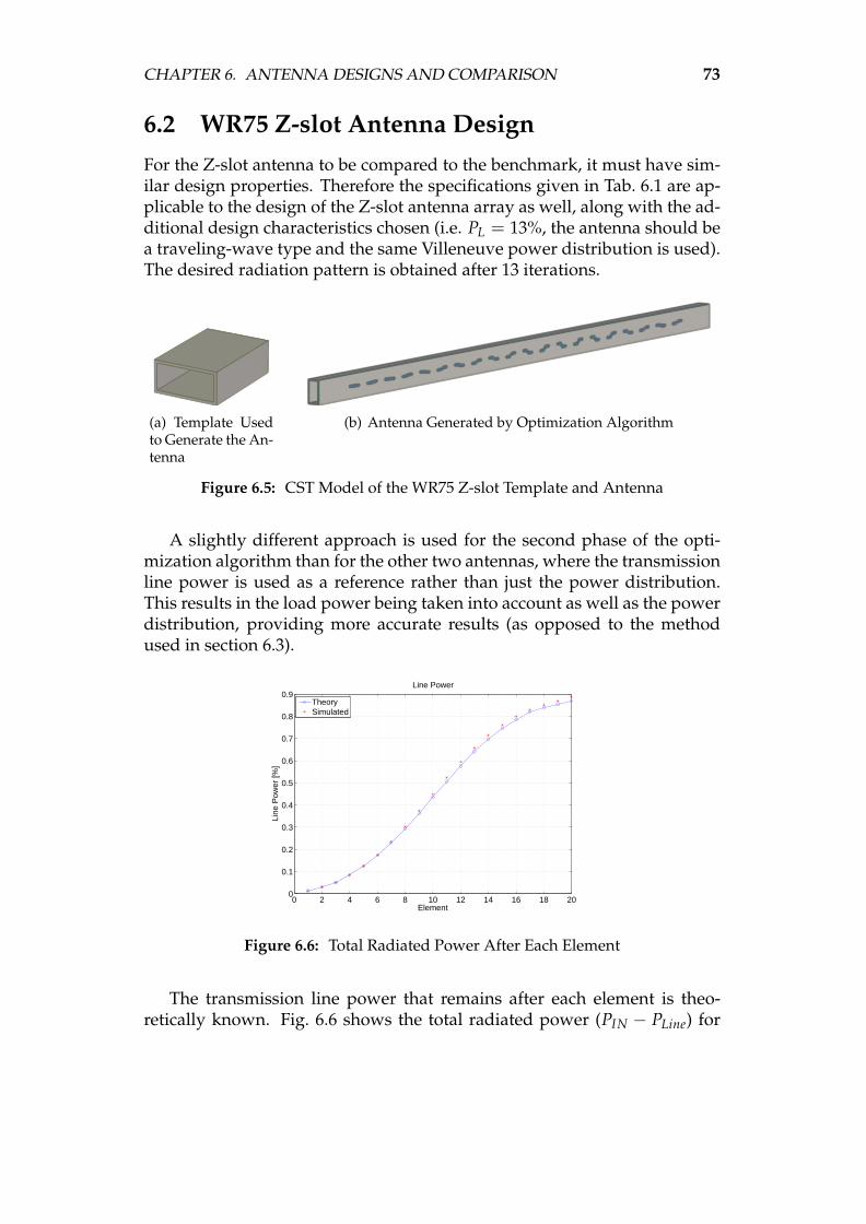
CHAPTER 6. ANTENNA DESIGNS AND COMPARISON 73
6.2 WR75 Z-slot Antenna DesignFor the Z-slot antenna to be compared to the benchmark, it must have sim-ilar design properties. Therefore the specifications given in Tab. 6.1 are ap-plicable to the design of the Z-slot antenna array as well, along with the ad-ditional design characteristics chosen (i.e. PL = 13%, the antenna should bea traveling-wave type and the same Villeneuve power distribution is used).The desired radiation pattern is obtained after 13 iterations.
(a) Template Usedto Generate the An-tenna
(b) Antenna Generated by Optimization Algorithm
Figure 6.5: CST Model of the WR75 Z-slot Template and Antenna
A slightly different approach is used for the second phase of the opti-mization algorithm than for the other two antennas, where the transmissionline power is used as a reference rather than just the power distribution.This results in the load power being taken into account as well as the powerdistribution, providing more accurate results (as opposed to the methodused in section 6.3).
0 2 4 6 8 10 12 14 16 18 200
0.1
0.2
0.3
0.4
0.5
0.6
0.7
0.8
0.9
Element
Line
Pow
er [%
]
Line Power
TheorySimulated
Figure 6.6: Total Radiated Power After Each Element
The transmission line power that remains after each element is theo-retically known. Fig. 6.6 shows the total radiated power (PIN − PLine) for

CHAPTER 6. ANTENNA DESIGNS AND COMPARISON 74
the final iteration. A power balance can more easily be seen for traveling-wave antennas using this method than when only the element distributionis taken into account. The load power is PL = 11.4% of the input power.
Fig. 6.7 shows the magnitude of the element impedances over all itera-tions and for the final iteration. For low values the approximations and gridadaptations appear to have difficulty describing the actual behavior of theZ-slot apertures; this can be seen from the large range of values and the lackof convergence for lower values. The second phase tuning takes care of thisdiscrepancy and provides adequate results.
The element phases are shown in Fig. 6.8. Both the impedance magni-tude and phase results indicate that a reasonable level of accuracy is ob-tained. The average phase is accurate to within 3 and the magnitude towithin 5% of the desired values.
The radiation pattern shown in Fig. 6.9 is within specifications. The pat-tern is calculated using only the main polarization component. The effectof the cross-polarization component on the radiation pattern is discussed insection 6.4.

CHAPTER 6. ANTENNA DESIGNS AND COMPARISON 75
0 5 10 15 200
0.05
0.1
0.15
0.2
0.25
0.3
0.35
Element Number
Impe
danc
e M
agni
tude
[Z]
Equivalent Impedances
Theory (Iter. 1)|Z| iteration: 1|Z| iteration: 2|Z| iteration: 3|Z| iteration: 4|Z| iteration: 5|Z| iteration: 6|Z| iteration: 7|Z| iteration: 8|Z| iteration: 9|Z| iteration: 10|Z| iteration: 11|Z| iteration: 12|Z| iteration: 13
(a) Simulated Magnitudes Over All Iterations
0 5 10 15 200
0.05
0.1
0.15
0.2
0.25
0.3
0.35
Element Number
Impe
danc
e M
agni
tude
[Z]
Equivalent Impedances
Theory (Iter. 1)|Z| iteration: 13
(b) Simulated Magnitude for Final Iteration
Figure 6.7: Simulated Magnitudes for All Iterations of the WR75 Z-slot Antenna

CHAPTER 6. ANTENNA DESIGNS AND COMPARISON 76
0 5 10 15 20−20
−10
0
10
20
30
40
50
60
70
Element Number
Pha
se E
rror
[deg
]
Phase Error in Simulation
Error Iteration: 1Error Iteration: 2Error Iteration: 3Error Iteration: 4Error Iteration: 5Error Iteration: 6Error Iteration: 7Error Iteration: 8Error Iteration: 9Error Iteration: 10Error Iteration: 11Error Iteration: 12Error Iteration: 13
(a) Simulated Phases Over All Iterations
0 5 10 15 20−5
−4
−3
−2
−1
0
1
2
3
Element Number
Pha
se E
rror
[deg
]
Phase Error in Simulation
Error Iteration: 13
(b) Simulated Phase for Final Iteration
Figure 6.8: Simulated Phases for All Iterations of the WR75 Z-slot Antenna

CHAPTER 6. ANTENNA DESIGNS AND COMPARISON 77
−50 0 50−50
−45
−40
−35
−30
−25
−20
−15
−10
−5
0
Angle [degrees]
Gai
n P
atte
rn [d
B]
Simulated Gain Patterns
Gain (Theory) FF: Iter 13
Figure 6.9: Radiation Pattern for the WR75 Z-slot Design

CHAPTER 6. ANTENNA DESIGNS AND COMPARISON 78
6.3 Ridged Waveguide Z-slot Antenna DesignThe template is provided for the ridged waveguide Z-slot design and theresulting antenna is shown in Fig. 6.10.
(a) Template Usedto Generate the An-tenna
(b) Antenna Generated by Optimization Algorithm
Figure 6.10: CST Model of the Ridged Waveguide Z-slot Template and Antenna
The desired performance is obtained after 16 iterations for the ridgedwaveguide Z-slot antenna. Again the initial error can be attributed to theaperture characterization neglecting to take mutual coupling into account.It can also be seen from Fig. 6.11(a) that the magnitude took longer to con-verge to the desired values than for the benchmark in Fig. 6.2(a).
Note that the values converge and then diverge again in later iterations.This is because the second phase of the tuning alters the magnitude basedonly on the aperture weighting. The load power is now incorrect (only PL =7.9%), since the elements radiate more power than they are intended to. Thefinal magnitudes shown in Fig. 6.11(b) shows this weighting.
The phase error over all iterations is shown in Fig. 6.12(a). It can beseen that the lower impedance elements (placed at the ends of the array)are particularly sensitive to phase errors. Initial phase errors as high asθerr = 85 is observed for the initial iterations. The final phase values shownin Fig. 6.12(b) are reasonable compared to the initial values. Again, thesecond tuning phase change the aperture impedance values significantly,which also affects the phase.
The radiation pattern shown in Fig. 6.13 shows that despite the double-edged nature of the second tuning phase, the desired pattern can be ob-tained. A sidelobe level of -32 dB is obtained for the Z-slot antenna, whichcompares well to the results of the benchmark antenna.
For the sake of interest, the aperture excitations are shown in Fig. 6.14.This is to show the focus of the optimization algorithm during the sec-ond phase. Once the iterations converge during the first phase to theimpedances based on the grid predictions, the focus is shifted away fromimpedance and rather to the aperture excitation weightings. Fig. 6.14(a)shows that the values converge to a weighting pattern that does not corre-spond to the desired weighting. However, after the second phase is started

CHAPTER 6. ANTENNA DESIGNS AND COMPARISON 79
0 5 10 15 200
0.05
0.1
0.15
0.2
0.25
0.3
0.35
Element Number
Impe
danc
e M
agni
tude
[Z]
Equivalent Impedances
Theory (Iter. 1)|Z| iteration: 1|Z| iteration: 2|Z| iteration: 3|Z| iteration: 4|Z| iteration: 5|Z| iteration: 6|Z| iteration: 7|Z| iteration: 8|Z| iteration: 9|Z| iteration: 10|Z| iteration: 11|Z| iteration: 12|Z| iteration: 13|Z| iteration: 14|Z| iteration: 15|Z| iteration: 16
(a) Simulated Magnitudes Over All Iterations
0 5 10 15 200
0.05
0.1
0.15
0.2
0.25
0.3
0.35
Element Number
Impe
danc
e M
agni
tude
[Z]
Equivalent Impedances
Theory (Iter. 1)|Z| iteration: 16
(b) Simulated Magnitude for Final Iteration
Figure 6.11: Simulated Magnitudes for All Iterations of the Ridged WaveguideZ-slot Antenna

CHAPTER 6. ANTENNA DESIGNS AND COMPARISON 80
0 5 10 15 20−40
−20
0
20
40
60
80
100
Element Number
Pha
se E
rror
[deg
]
Phase Error in Simulation
Error Iteration: 1Error Iteration: 2Error Iteration: 3Error Iteration: 4Error Iteration: 5Error Iteration: 6Error Iteration: 7Error Iteration: 8Error Iteration: 9Error Iteration: 10Error Iteration: 11Error Iteration: 12Error Iteration: 13Error Iteration: 14Error Iteration: 15Error Iteration: 16
(a) Simulated Phases Over All Iterations
0 5 10 15 20−10
−5
0
5
Element Number
Pha
se E
rror
[deg
]
Phase Error in Simulation
Error Iteration: 16
(b) Simulated Phase for Final Iteration
Figure 6.12: Simulated Phases for All Iterations of the Ridged WaveguideZ-slot Antenna

CHAPTER 6. ANTENNA DESIGNS AND COMPARISON 81
−50 0 50−50
−45
−40
−35
−30
−25
−20
−15
−10
−5
0
Angle [degrees]
Gai
n P
atte
rn [d
B]
Simulated Gain Patterns
Gain (Theory) FF: Iter 16
Figure 6.13: Radiation Pattern for the Ridged Waveguide Z-slot Design
(at iteration 14), the pattern converges in only 3 iterations and is shown inFig. 6.14(b). The final load power is PL = 7.9%, which is lower than thedesign value of PL = 13%, due to the higher aperture impedance values.
Although the two tuning phases are performing as they are designedto, the algorithm admittedly needs to be adapted to simultaneously lookat both the impedances and the excitation weightings. The transmissionline method used in section 6.2 is one possible solution, where both theweighting and the load power is considered simultaneously.

CHAPTER 6. ANTENNA DESIGNS AND COMPARISON 82
0 5 10 15 200
0.1
0.2
0.3
0.4
0.5
0.6
0.7
0.8
0.9
1
Element Number
Nor
mal
ized
V−
Wei
ghtin
g
Voltage Weighting over Slots
TheoryE−Field: 1E−Field: 2E−Field: 3E−Field: 4E−Field: 5E−Field: 6E−Field: 7E−Field: 8E−Field: 9E−Field: 10E−Field: 11E−Field: 12E−Field: 13E−Field: 14E−Field: 15E−Field: 16
(a) Simulated Weighting Over All Iterations
0 5 10 15 200.1
0.2
0.3
0.4
0.5
0.6
0.7
0.8
0.9
1
Element Number
Nor
mal
ized
V−
Wei
ghtin
g
Voltage Weighting over Slots
TheoryE−Field: 16
(b) Simulated Weighting for Final Iteration
Figure 6.14: Simulated Excitation Weightings for All Iterations of theZ-slot Antenna

CHAPTER 6. ANTENNA DESIGNS AND COMPARISON 83
6.4 Comparison of Benchmark andZ-slot Antenna Properties
The benchmark and Z-slot antennas all adhere to the minimum design spec-ifications given in Tab. 6.1. It is now possible to compare their performancecharacteristics on an objective scale.
Only the broad wall radiation patterns were considered during the de-sign process. Fig. 6.15 shows the 3D radiation patterns for all three antennas.
(a) Benchmark 3D Radiation Pattern (b) Z-slot Ridge 3D Radiation Pattern
(c) Z-slot WR75 3D Radiation Pattern
Figure 6.15: 3D Radiation Patterns
Note that the sidelobe in the elevation direction of the benchmark design(Fig. 6.15(a)) is all but removed from the ridged Z-slot antenna (Fig. 6.15(b)),yet still present in the WR75 Z-slot antenna.
Fig. 6.16 shows the radiation pattern for all three antennas with boththe desired and cross-polarizations. The desired polarization is labeled as“phi” and the cross-polarization is labeled as “theta”. The main polarization
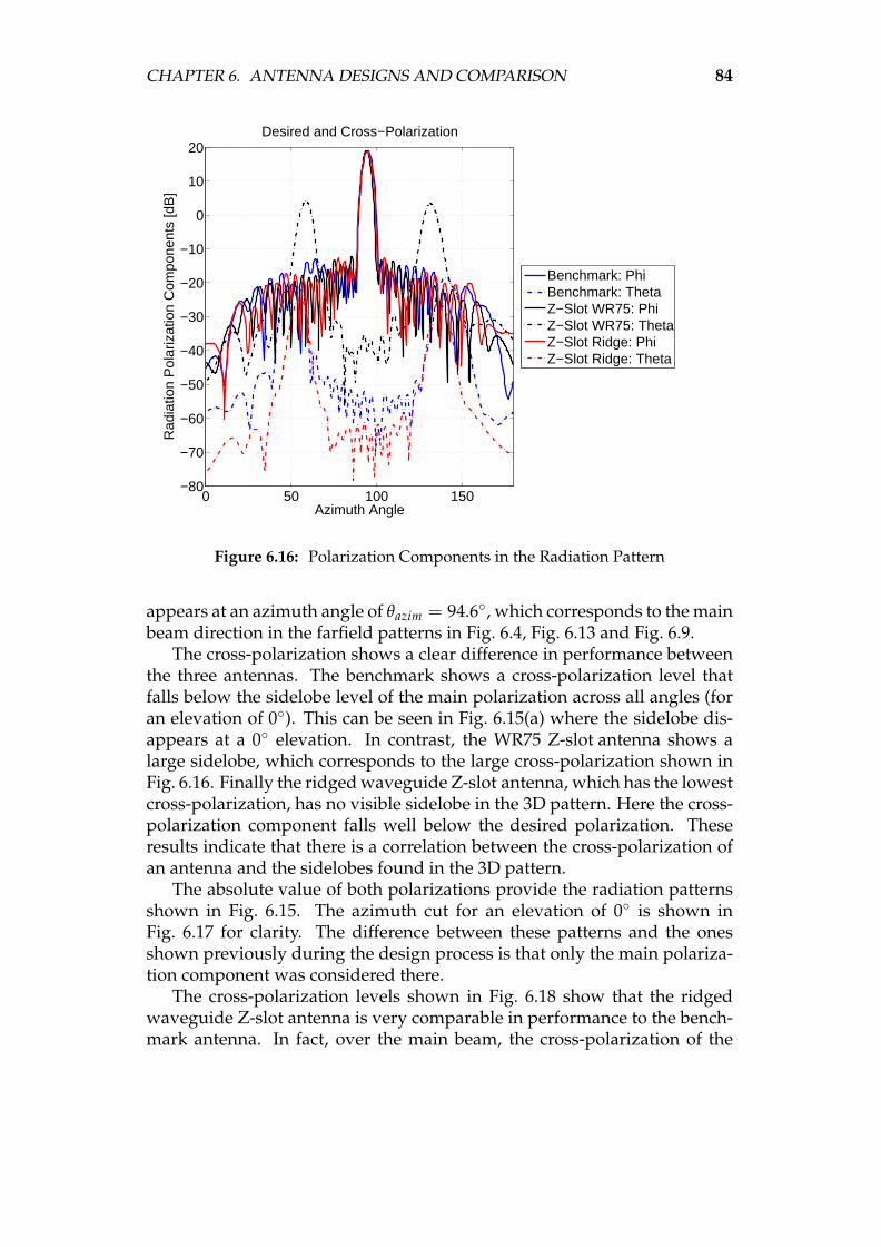
CHAPTER 6. ANTENNA DESIGNS AND COMPARISON 84
0 50 100 150−80
−70
−60
−50
−40
−30
−20
−10
0
10
20
Azimuth Angle
Rad
iatio
n P
olar
izat
ion
Com
pone
nts
[dB
]
Desired and Cross−Polarization
Benchmark: PhiBenchmark: ThetaZ−Slot WR75: PhiZ−Slot WR75: ThetaZ−Slot Ridge: PhiZ−Slot Ridge: Theta
Figure 6.16: Polarization Components in the Radiation Pattern
appears at an azimuth angle of θazim = 94.6, which corresponds to the mainbeam direction in the farfield patterns in Fig. 6.4, Fig. 6.13 and Fig. 6.9.
The cross-polarization shows a clear difference in performance betweenthe three antennas. The benchmark shows a cross-polarization level thatfalls below the sidelobe level of the main polarization across all angles (foran elevation of 0). This can be seen in Fig. 6.15(a) where the sidelobe dis-appears at a 0 elevation. In contrast, the WR75 Z-slot antenna shows alarge sidelobe, which corresponds to the large cross-polarization shown inFig. 6.16. Finally the ridged waveguide Z-slot antenna, which has the lowestcross-polarization, has no visible sidelobe in the 3D pattern. Here the cross-polarization component falls well below the desired polarization. Theseresults indicate that there is a correlation between the cross-polarization ofan antenna and the sidelobes found in the 3D pattern.
The absolute value of both polarizations provide the radiation patternsshown in Fig. 6.15. The azimuth cut for an elevation of 0 is shown inFig. 6.17 for clarity. The difference between these patterns and the onesshown previously during the design process is that only the main polariza-tion component was considered there.
The cross-polarization levels shown in Fig. 6.18 show that the ridgedwaveguide Z-slot antenna is very comparable in performance to the bench-mark antenna. In fact, over the main beam, the cross-polarization of the

CHAPTER 6. ANTENNA DESIGNS AND COMPARISON 85
0 20 40 60 80 100 120 140 160 180−60
−50
−40
−30
−20
−10
0
10
20
Azimuth Angle
Dire
ctiv
ity [d
B]
Absolute Radiation Pattern
BenchmarkZ−Slot WR75Z−Slot Ridge
Figure 6.17: Absolute Radiation Pattern Including Both Polarization Components
0 20 40 60 80 100 120 140 160 180
−80
−60
−40
−20
0
20
40
Azimuth Angle
Cro
ss−
Pol
ariz
atio
n Le
vel [
dB]
Azimuth Cross−Polarization Level
BenchmarkZ−Slot WR75Z−Slot Ridge
Figure 6.18: Cross-Polarization Level in the Azimuth Cut

CHAPTER 6. ANTENNA DESIGNS AND COMPARISON 86
ridged waveguide Z-slot antenna is more than 8.5 dB lower than the bench-mark. It should also be noted that the WR75 Z-slot antenna (which is alinear array), does not perform as well as the benchmark antenna, indicat-ing that the linear array assumption is not at fault for the appearance of thesidelobes but rather the cross-polarization.
0 20 40 60 80 100 120 140 160 180−70
−60
−50
−40
−30
−20
−10
0
10
20Absolute Patterns: Horizontal
Theta [deg]
Dire
ctiv
ity [d
B]
BenchmarkZ−Slot WR75Z−Slot Ridge
Figure 6.19: Horizontal Cut (φ = 0o) of Radiation Pattern for All Designs
0 20 40 60 80 100 120 140 160 180−60
−50
−40
−30
−20
−10
0
10
20Absolute Patterns: Diagonal (45o)
Theta [deg]
Dire
ctiv
ity [d
B]
BenchmarkZ−Slot WR75Z−Slot Ridge
Figure 6.20: Diagonal Cut (φ = 45o) of Radiation Pattern for All Designs

CHAPTER 6. ANTENNA DESIGNS AND COMPARISON 87
0 20 40 60 80 100 120 140 160 180−50
−40
−30
−20
−10
0
10
20Absolute Patterns: Vertical
Theta [deg]
Dire
ctiv
ity [d
B]
BenchmarkZ−Slot WR75Z−Slot Ridge
Figure 6.21: Vertical Cut (φ = 90o) of Radiation Pattern for All Designs
In Figs. 6.19–6.21, the absolute radiation pattern cut is shown for differ-ent elevations. Three elevations are given, namely “Horizontal”, “Diago-nal” and “Vertical”. The horizontal cut (Fig. 6.19) refers to an elevation ofφ = 0o, which corresponds to the same cut used during the design process.The diagonal cut (Fig. 6.20) looks at the radiation patter at φ = 45o, wherethe 3D radiation pattern indicates the sidelobes are already quite promi-nent. The vertical cut (Fig. 6.19) corresponds to φ = 90o, which is the planetangential to the desired radiation direction.
These plots indicate how well the Z-slot antenna with polarizer platessupress the undesired sidelobes. Note that this is the absolute pattern, notjust the desired polarization. For all practical purposes, the ridged waveg-uide Z-slot antenna completely suppresses the sidelobes in the 3D pattern(for the cuts shown) and keeps the sidelobe level to below the −30 dB crite-ria.

Chapter 7
Conclusions
7.1 SummaryFor a radar antenna to be effective, it was argued in chapter 1 that the ra-diation pattern must be precisely designed and that the presence of side-lobes are undesired. Unwanted sidelobes have been observed in slottedwaveguide designs for the standard rectangular offset slots in a rectangularwaveguide. The possible cause of these sidelobes were hypothesized to beattributed to
1. cross-polarization and
2. the incorrect assumption of a linear array.
By isolating the cause of the sidelobes, a design procedure that takes theeffect of cross-polarization into account could be developed to generate anantenna with the desired radiation pattern properties.
The steps involved in determining the cause of the undesired sidelobesinvolved a very practical approach. A typical antenna with offset rectan-gular apertures is taken as a benchmark with which to compare the resultsof other designs. The benchmark is broken down into its base components(namely the waveguide and the apertures) and investigated separately.
The waveguide is assumed to have no contribution to the polarizationproperties of the antenna, as the propagation mode by definition suppressesthe undesired polarization component (i.e. the E-field in the direction ofpropagation). However, the design specification in Tab. 1.1 is consideredand a custom waveguide profile is designed to conform to specifications. Aridged waveguide is found that has the correct operating frequency, band-width and tolerance bands.
The isolated offset rectangular aperture is investigated, along with theZ-slot . Polarization properties, radiation capacity and bandwidth proper-ties of the apertures are discussed for various configurations. The effect ofadding polarization plates to the Z-slot is also investigated. It was found
88

CHAPTER 7. CONCLUSIONS 89
that by adding polarizer plates of increasing lengths, the unwanted polar-ization component of the Z-slot could be significantly suppressed. This re-sult, in conjunction with the ridged waveguide design, provided the basecomponents used for the low cross-polarization design. A linear array de-sign is also completed (with poor cross-polarization levels).
The final antennas that were designed includes: a benchmark antennausing offset rectangular apertures; a Z-slot array in WR75; and a Z-slot arrayin a ridged waveguide with polarizer plates. The two Z-slot antennasserve to investigate whether it is the cross-polarization or the offsets of therectangular apertures that cause the unwanted sidelobes. The low cross-polarization antenna showed significant improvement in the sidelobe level,where the “linear array” antenna showed a deterioration in performance.The conclusion that can be drawn from this is that by suppressing the cross-polarization, the unwanted sidelobes can be suppressed.
A ridged waveguide Z-slot antenna with polarizer plates is provided asa possible alternative to the offset aperture antenna. All of the performanceproperties compare well to the benchmark antenna, with the exception thatthe unwanted sidelobes are suppressed by approximately 15 – 20 dB.
7.2 Recommendations for Future ResearchAs is often the case, by answering one question two more are asked. Theresults shown here serve to indicate a trend in antenna behavior based onthe polarization properties of a linear array. However, the precise extentto which the polarization affects the radiation pattern of an antenna is notdiscussed, nor is the possibility that the linear array is inaccurate completelyeliminated.
Further investigation into the precise effect of the cross-polarization onthe radiation pattern of an antenna should be conducted. Also, the onlysuppression technique considered here are the polarizing plates around aZ-slot antenna. More generic polarizers can be considered to further helpimprove the performance of the antenna.
The assumption that all radiators are placed in a straight line may stillcontribute to some extent to the poor sidelobe level of the offset rectangu-lar aperture antenna. The limits of this approximation must be determined,particularly for arrays with a low number of elements (i.e. with large aper-ture offsets).
An improved method of characterizing arbitrary aperture configura-tions will serve to improve the first order design of an array. The apertureswere either characterized as a parallel or series impedance, where complexapertures may perform more like a T or Π network. By accurately deter-mining the equivalent network, better first-order designs can be made.

CHAPTER 7. CONCLUSIONS 90
The optimization algorithm is very simple in comparison to some of theadvanced methods being developed in the world. More intelligent algo-rithms should be considered to reduce the number of iterations necessaryto obtain convergence. The current method relies on a priori knowledgeof how the apertures operate, which is undesirable. An improved optimiza-tion algorithm will be independent of the equivalent network of an apertureor its behavior.
A general design approach may be also be investigated, where theridged waveguide is turned on its head and the slots inserted into thetrough of the ridge. By extending the outside of the ridge, the polarizerplates become a natural extension of the waveguide, making it more com-pact and lighter. The reason this was note done here is because it was dif-ficult to model in CST. It may be possible that a different simulation toolcould be used, alternatively the model may include a waveguide transitioncould be included (such as the one in Appendix D). This approach wouldlikely make for a more practical antenna with much the same performancecharacteristics as the ridged waveguide antenna designed here.
7.3 ConclusionThe aim of the research conducted was to gain a greater understanding ofslotted waveguide antennas along with the appearance of undesired side-lobes. Two possible causes to the sidelobes were hypothesized and system-atically investigated. Several antennas were designed to verify the effectof the varying elements in a design (e.g. the waveguide profile, the aper-ture chosen and the polarizer plates). The resulting antennas both served todeepen the understanding of the problem, as well as to provide an alterna-tive to the current design method used.

Appendices
91

Appendix A
Benchmark Design
A.1 IntroductionThe dimensions for manufacture and the expected results are provided here.Note that no tolerances were considered and that results are subject to varydue to measurement and manufacturing errors. Fig. A.1 shows a depictionof the antenna.
Figure A.1: Model of the Benchmark Antenna
A.2 DimensionsTab. A.1 provides the offsets and aperture lengths for the rectangular offsetapertures inset into a rectangular waveguide. The element numbering startsfrom the source and increase toward the terminating load. The apertureshave angled corners, as this is the most commonly found aperture in theliterature. Milling such an aperture could be difficult and would commonlyhave rounded corners. The width of the aperture is ap_width = 2 mm forall elements. Elements are spaced elem_sp = 20.40175 mm apart from thecenter of each element.
92

APPENDIX A. BENCHMARK DESIGN 93
Table A.1: Dimensions of Benchmark Apertures
Element No. Offset [mm] Length [mm]1 0.5892 13.599242 0.6925 13.616373 0.8755 13.616374 1.4579 13.616375 1.5976 13.633506 2.1541 13.633507 2.3786 13.684878 2.7279 13.734829 3.0653 13.78620
10 3.3758 13.8033311 3.7711 13.8375812 4.1468 13.8547013 4.5320 13.8718314 4.6050 13.8889515 4.3998 13.8718316 3.9677 13.8375817 3.3063 13.7862018 2.3613 13.7005719 1.8018 13.6335020 1.7369 13.63350
A standard WR90 profile is used, with a wall thickness of th = 1 mm.The inside dimensions of the profile are 22.86× 10.16 mm. The total lengthof the antenna is length = 469.2403 mm.
A.3 Simulated ResultsThe radiation pattern shown in Fig. A.3 shows the accuracy of the model inthe azimuth direction as well as the 3D radiation pattern that exhibits theundesired sidelobes.
Fig. A.2(a) clearly shows the sidelobes at about 10 – 13 dB below themain lobe. The pattern in the azimuth cut shown in Fig. A.2(b) shows howwell the designed pattern conforms to the theoretical pattern. The resultsindicated that all values are within tolerance and that the antenna performsas expected.

APPENDIX A. BENCHMARK DESIGN 94
(a) 3D Radiation Pattern
−50 0 50−50
−45
−40
−35
−30
−25
−20
−15
−10
−5
0
Theta [degrees]
Gai
n P
atte
rn [d
B]
Simulated Gain Patterns
Gain (Theory) FF: Iter 10
(b) Azimuth Radiation Pattern

Appendix B
WR75 Waveguide Z-slot Design
B.1 IntroductionThe dimensions for manufacture and the expected results are provided here.Note that no tolerances were considered and that results are subject to varydue to measurement and manufacturing errors. Fig. B.1 shows a depictionof the antenna.
Figure B.1: Model of the WR75 Z-slot Antenna
A standard WR75 profile is used, with a wall thickness of th = 1 mm.The inside dimensions of the profile are 19.05× 9.525 mm. The total lengthof the antenna is length = 553.3372 mm.
B.2 DimensionsTab. B.1 provides the rotation angles (in degrees) of the apertures as well astheir lengths. The element numbering starts from the source and increasetoward the terminating load. The angle is defined in Fig. 4.1.
95

APPENDIX B. WR75 WAVEGUIDE Z-SLOT DESIGN 96
Table B.1: Dimensions of Z-slot Apertures in WR75
Element No. Angle [deg] Length [mm]1 87.6702 12.280564292 85.3467 12.193508573 82.0847 12.223478574 78.6415 12.242031435 74.9699 12.209207146 71.3257 12.232041437 68.0284 12.291981438 64.7099 12.336222869 60.9176 12.43612286
10 56.0933 12.5774111 49.83 12.7429585712 42.6051 12.9284871413 37.438 13.0883271414 35.3394 13.1425585715 37.7259 13.0783371416 45.1924 12.8799642917 56.6297 12.6930085718 64.6498 12.5916814319 68.5645 12.5717014320 69.0049 12.57027429
B.3 Simulated ResultsThe radiation pattern shown in Fig. B.3 shows the accuracy of the model inthe azimuth direction as well as the 3D radiation pattern that exhibits theundesired sidelobes.
Fig. B.2(a) shows the undesired sidelobes are present at a level of approx-imately 15 dB below the main lobe. The pattern in the azimuth cut shownin Fig. C.3(b) shows how well the designed pattern conforms to the theoret-ical pattern. The results indicated that all values are within tolerance andthat the antenna performs as expected. Note that in the case of Fig. B.2(b),the pattern is calculated only with the Ex component, which is why it dif-fers from the 3D pattern. The sidelobes here are therefore a result of thecross-polarization component.

APPENDIX B. WR75 WAVEGUIDE Z-SLOT DESIGN 97
(a) 3D Radiation Pattern
−50 0 50−50
−45
−40
−35
−30
−25
−20
−15
−10
−5
0
Angle [degrees]
Gai
n P
atte
rn [d
B]
Simulated Gain Patterns
Gain (Theory) FF: Iter 13
(b) Azimuth Radiation Pattern

Appendix C
Ridged Waveguide Z-slot Design
C.1 IntroductionThe dimensions for manufacture and the expected results are provided here.Note that no tolerances were considered and that results are subject to varydue to measurement and manufacturing errors. Fig. C.1 shows a depictionof the antenna. The waveguide used is not standard, so it must be extrudedfor best results. The polarizer plates may cause difficulties in milling theapertures, otherwise they may be attached after milling.
Figure C.1: Model of the Ridged Waveguide Z-slot Antenna
C.2 DimensionsTab. C.1 provides the rotation angles (in degrees) of the apertures as well astheir lengths. The element numbering starts from the source and increasetoward the terminating load. The angle is defined in Fig. 4.1.
The profile is designed to conform to the specifications of Tab. 1.1. Thedimensions are given in Fig. C.2 and include the polarizer dimensions used.
The wall thickness is again th = 1 mm. The element spacing iselem_sp = 21.79581 mm and the total length of the antenna is length =501.3036 mm. Apertures are ap_width = 2 mm for all elements.
98

APPENDIX C. RIDGED WAVEGUIDE Z-SLOT DESIGN 99
Table C.1: Dimensions of Z-slot Apertures in a Ridged Waveguide
Element No. Angle [deg] Length [mm]1 84.7445 16.412142 83.6496 16.412143 80.8029 16.412144 77.9562 16.412145 75.7664 15.905516 73.7956 15.468807 71.6058 15.191948 69.6350 14.962179 67.4453 14.82373
10 65.0365 14.7324011 62.6277 14.6396312 60.0000 14.5939613 57.8102 14.5711314 56.9343 14.5711315 58.0292 14.5711316 61.7518 14.6168017 66.3504 14.7780618 71.1679 15.1462719 75.3285 15.7913420 76.6423 16.18237
Figure C.2: Waveguide Profile for the Ridged Waveguide Z-slot Antenna

APPENDIX C. RIDGED WAVEGUIDE Z-SLOT DESIGN 100
C.3 Simulated ResultsThe radiation pattern shown in Fig. C.3 shows the accuracy of the model inthe azimuth direction as well as the 3D radiation pattern that exhibits theundesired sidelobes.
Fig. C.3(a) shows the sidelobes are suppressed to approximately 25 –30 dB below the main lobe. The pattern in the azimuth cut shown inFig. C.3(b) shows how well the designed pattern conforms to the theoret-ical pattern. The results indicated that all values are within tolerance andthat the antenna performs as expected.

APPENDIX C. RIDGED WAVEGUIDE Z-SLOT DESIGN 101
(a) 3D Radiation Pattern
−50 0 50−50
−45
−40
−35
−30
−25
−20
−15
−10
−5
0
Angle [degrees]
Gai
n P
atte
rn [d
B]
Simulated Gain Patterns
Gain (Theory) FF: Iter 16
(b) Azimuth Radiation Pattern

Appendix D
WR90 to Ridged WaveguideTransition
The CST simulations included an artificial termination load and feed port.This is convenient for simulation purposes in that it reduces the complexityof the model, but makes for an incomplete real-world design. In order tobuild and test the antennas designed using the ridged waveguide, it is nec-essary to find a means of feeding the antenna and to absorb the energy atthe terminating port.
For this purpose a waveguide transition was designed using FEKO, acomputational tool similar to CST. The results were optimized to transferthe maximum power at f0. The reflection coefficient, which in this caseequals S11, is shown in Fig. D.1. It can be seen that at f = 10.5 = f0, most ofthe input power is absorbed by the output port depicted in Fig. D.2.
It should be noted that Fig. D.2 illustrates the two uses of the transition:primarily as a feed for the antenna, but also as a terminating load at the endof the antenna. In other words, the model in Fig. D.2 can be split in halfand two elements must be manufactured. The first element will port energypropagating down a standard WR90 profile to the custom ridge profile. Theterminating load will be attached to the end of the antenna, along with aWR90 terminating load attached.
The transition is made up of three sections:
• a WR90 section;
• a transition from WR90 to the ridged profile; and
• a ridged profile section.
Each of these sections is secLen = 14.61457 mm = 0.511864×λ long. It isthis value that is optimized to provide the desired operating frequency. Allother dimensions correspond to the respective profile dimensions. Furtherimages of a transition is shown in Fig. D.3.
102

APPENDIX D. WR90 TO RIDGED WAVEGUIDE TRANSITION 103
Figure D.1: Magnitude of S11
Figure D.2: Two-port Model for the Waveguide Transition

APPENDIX D. WR90 TO RIDGED WAVEGUIDE TRANSITION 104
(a) 3D View (b) Top View
(c) Side View (d) Front View
Figure D.3: Single-Ended WR90 to Ridged Waveguide Transition

Bibliography
[1] M. Skolnik, Introduction to Radar Systems, 3rd ed. McGraw Hill, 2001.
[2] “Private communication.”
[3] R. Elliot, Antenna Theory and Design. Prentice Hall, 1981.
[4] D. Howard, Ed., Dictionary of Electronics, 4th ed. Penguin Reference,2005.
[5] D. Pozar, Microwave Engineering, 3rd ed. John Wiley & Sons, 2005.
[6] S. Ramo, J. Whinnery, and T. van Duzer, Fields and Waves in Communi-cation Electronics. John Wiley & Sons, 1994.
[7] W. Hoefer and M. Burton, “Closed-form expressions for the parame-ters of finned and ridged waveguides,” IEEE Transactions on MicrowaveTheory and Techniques, vol. MTT30, no. 12, pp. 2190–2194, Dec 1982.
[8] S. Hopfer, “The design of ridged waveguides,” Transactions on Mi-crowave Theory and Techniques, vol. 3.5, pp. 20–29, Oct. 1955.
[9] H. Booker, “Slot aerials and their relation to complementary wire aeri-als,” J. IEE (London), vol. 93, pp. 620–626, Dec 1946.
[10] G. Deschamps, “Impedance properties of complementary multitermi-nal planar structures,” IRE Transactions on Antennas and Propagation,vol. 7, pp. 371–378, 1959.
[11] A. Stevenson, “Theory of slots in rectangular wave-guides,” Journal ofApplied Physics, vol. 19, pp. 24 – 38, 1948.
[12] A. Oliner, “The impedance properties of narrow radiating slots in thebroad face of rectangular waveguide: Part i–theory,” IRE Trans. Anten-nas Propagat., vol. 5, pp. 4–11, Jan. 1957.
[13] ——, “The impedance properties of narrow radiating slots in the broadface of rectangular waveguide: Part ii–comparison with measure-ment,” IRE Trans. Antennas Propagat., vol. 5, pp. 12–20, Jan. 1957.
105

BIBLIOGRAPHY 106
[14] ——, “Equivalent circuits for small symmetrical longitudinal aperturesand obstacles,” Transactions on Microwave Theory and Techniques, vol. 8.1,pp. 72–80, Jan. 1960.
[15] J. Gulick, G. Stern, and R. Elliot, “The equivalent circuit of arectangular-waveguide-fed longitudinal slot,” IEEE Int. Antennas Prop-agat., vol. 24, pp. 685–688, Jun. 1986.
[16] C. Balanis, Antenna Theory, 3rd ed. John Wiley & Sons, 2005.
[17] A. Villeneuve, “Taylor patterns for discrete arrays,” IEEE Trans. Anten-nas Propagat., vol. 32, pp. 1089–1093, Oct. 1984.
[18] J. Volakis, Antenna Engineering Handbook, 4th ed. McGraw Hill, 2007.
[19] D. Kim and R. Elliott, “A design procedure for slot arrays fed by single-ridge waveguide,” IEEE Int. Antennas Propagat., vol. 36, pp. 1531–1536,November 1988.
[20] (2009, Sept) Rectangular waveguide dimensions. Mi-crowave Encyclopedia - Microwaves 101. [Online]. Available:http://www.microwaves101.com/encyclopedia/waveguidedimensions.cfm

![A 140 GHz High Efficiency Slotted Waveguide Antenna using ... · integrated waveguide (SIW) slot antenna array [6]-[8], and the 400 GHz folded reflectarray [9]. Among them, the slotted](https://static.fdocuments.net/doc/165x107/5f01d7e07e708231d4014f46/a-140-ghz-high-efficiency-slotted-waveguide-antenna-using-integrated-waveguide.jpg)


![A linearly slotted waveguide antenna and comparison of it with a … · Although slotted waveguide antennas are one of the oldest antenna types [1], they are still applied in telecommu-nication](https://static.fdocuments.net/doc/165x107/6119a3ff77ae5a635618e78d/a-linearly-slotted-waveguide-antenna-and-comparison-of-it-with-a-although-slotted.jpg)
![A 32-GHz Microstrip Array Antenna for Microspacecraft ... · A 32-GHz Microstrip Array Antenna for Microspacecraft Application ... is the planar slotted waveguide array [2], ... posed](https://static.fdocuments.net/doc/165x107/5b344a987f8b9aa0238dc5e2/a-32-ghz-microstrip-array-antenna-for-microspacecraft-a-32-ghz-microstrip.jpg)