The Science and Engineering of Microelectronic Fabrication by Stephen A. Campbell
Chapter 2
UEEP2613
Microelectronic Fabrication
Lithography

Prepared by
Dr. Lim Soo King
24 Jun 2012

- i -
Chapter 2 Lithography ..................................................................... 47
2.0 Introduction .............................................................................................. 47
2.1 Requirements of Lithography ................................................................. 48
2.2 Photoresist ................................................................................................. 48
2.2.1 Polymer .............................................................................................................. 50 2.2.2 Sensitizer ............................................................................................................ 50 2.2.3 Solvent ................................................................................................................ 50
2.2.4 Additive .............................................................................................................. 50
2.3 Lithography Process ................................................................................ 51
2.3.1 Surface Preparation .......................................................................................... 52
2.3.2 Photoresist Coating ........................................................................................... 53 2.3.3 Soft Bake ............................................................................................................ 56 2.3.4 Alignment and Exposure .................................................................................. 57 2.3.5 Post Exposure Bake .......................................................................................... 66 2.3.6 Development ...................................................................................................... 67 2.3.7 Hard Bake .......................................................................................................... 68 2.3.8 Pattern Inspection ............................................................................................. 69
2.4 Electron Lithography............................................................................... 71
2.4.1 Raster and Vector Scans .................................................................................. 73
2.5 X-Ray Lithography .................................................................................. 74
2.5.1 Proximity Printing ............................................................................................ 76
2.5.2 X-Ray Mask ....................................................................................................... 77
2.6 Ion Lithography ....................................................................................... 78
Exercises .......................................................................................................... 80
Bibliography ................................................................................................... 82
- ii -
Figure 2.1: Pattern process with negative and positive photoresists .................................. 49 Figure 2.2: Resolution of negative and positive photoresists ............................................. 51 Figure 2.3: Flowchart of lithography processes ................................................................. 52 Figure 2.4: Thickness of photoresist and its relationship with spin rate and viscosity in
centi-Stoke ....................................................................................................... 54 Figure 2.5: Spin rate of dynamic dispensing ...................................................................... 55 Figure 2.6: Chemical edge-based removal ......................................................................... 55 Figure 2.7: Optical edge-based removal ............................................................................. 56 Figure 2.8: (a) Contact and (b) proximity printing ............................................................. 57
Figure 2.9: Schematic proximity printing .......................................................................... 58
Figure 2.10: Projection printing ........................................................................................... 59 Figure 2.11: Illustration of depth of focus ............................................................................ 60 Figure 2.12: Scanning projection printing ............................................................................ 62 Figure 2.13: Step and repeat exposure printing .................................................................... 63 Figure 2.14: A step and repeat alignment and exposure automatic system.......................... 64 Figure 2.15: Wavelength spectrum of mercury UV light source ......................................... 65 Figure 2.16: Standing wave effect induced intensity change ............................................... 66
Figure 2.17: Standing wave effect on photoresist ................................................................ 66
Figure 2.18: Schematic of a spinner developer system ........................................................ 68 Figure 2.19: Profile of photoresist caused by temperature and duration .............................. 68 Figure 2.20: Pinhole reflow by thermal flow of photoresist ................................................ 69
Figure 2.21: Photoresist reflow due to over bake ................................................................. 69 Figure 2.22: Various types of misalignment ........................................................................ 70
Figure 2.23: Good critical dimension and bad critical dimension........................................ 71 Figure 2.24: e-beam lithography system .............................................................................. 72
Figure 2.25: Flow of data in electron beam exposure systems ............................................. 73 Figure 2.26: The principles of raster and vector scan, (a) Raster scan and (b) Vector scan 74 Figure 2.27: Typical X-ray absorption coefficients with some lines characteristic of
commonly used materials ................................................................................ 75 Figure 2.28: X-ray shadowing errors and X-ray mask structure. (a) X-ray proximity
printing consideration, (b) X-ray mask structure ............................................. 76 Figure 2.29: Resolution and throughput in submicron region .............................................. 80
- 47 -
Chapter 2
Lithography
_____________________________________________
2.0 Introduction
The fabrication of integrated circuit IC both MOS and bipolar devices involves
a numbers of repeated major process steps. The processes can be broadly
classified into wafer cleaning process, lithography (imaging, resist-bleaching
and resist development), oxidation process, etching, diffusion/ion implantation,
chemical vapor deposition CVD of thin film deposition, epitaxial silicon and
polycrystalline process, physical vapor deposition/metal deposition or
evaporation/sputtering, thin film such as silicon nitride Si3N4, titanium nitride
TiN, Ti-W alloy, titanium silicide TiSi2, tungsten silicide WSi2 processes, and
sintering/rapid thermal annealing RTA.
Lithography is a process encompasses all the steps involved in transferring
a design pattern from a mask or reticle to the photoresist coated surface of
silicon wafer. This is also a process to create precise dimensioned open area on
silicon dioxide/silicon nitride or metallic surface. Opening on surface of silicon
dioxide will allow diffusion or ion implantation of impurities into the silicon.
The open area can be the opening for bond pad etc.
The process steps of lithography are cleaning wafer, deposit barrier layer of
silicon dioxide SiO2, silicon nitride Si3N4, metal, coating with photoresist, soft
bake, align mask, expose pattern, hard bake, develop photoresist, inspection. In
brief, lithography has three steps i.e. imaging, resist bleaching, and resist-
development.
In the modern era of VLSI/ULSI integration, lithography can be done in
several ways. Among the methods are direct writing and using mask. After the
pattern generator generated the circuit pattern, the pattern can be directly written
on the photoresist material film deposited on the surface of the wafer either by
light source, electron beam, ion beam, X-ray sources etc.
For the case of using mask, the mask is made from pattern generator and
uses light sources like ultraviolet light, ion beam, and X-ray as the exposure
source to impinge pattern on the photoresist. The mask is made by mask making
machine that transfer either an electron beam or laser pattern generator. It is
02 Lithography
- 48 -
usually made of fused silica plate covered with a thin layer 80nm of
chromium.
2.1 Requirements of Lithography
Lithography process requires high resolution, high sensitivity, precise
alignment, and low defect density. As the integration level is decreased, high
resolution and precise alignment are required. There is little room for alignment
error since the maximum tolerance is 10% of the critical dimension. Thus, for
advanced and sub-micron device lithography, it needs automatic alignment
system. This is a very challenging process step because one degree Celsius
difference in temperature for a wafer of diameter 200mm, it can cause a
difference of 0.5m in diameter due to thermal expansion of silicon that is
2.5x10⁻⁶
/0C.
Lithography process needs to minimize defect density since the defect
introduces in this process can be transferred to device and circuit via each
successive etch or ion implantation steps, and it affects the yield and reliability
of the device.
Since lithography is a high resolution process, it requires shorter
wavelength photon. Modern exposure system produces diffraction limited
image and diffraction effect is strongly related to wavelength of the exposing
radiation.
2.2 Photoresist
Photoresists are photosensitive materials used to temporarily coat on the surface
wafer and to transfer the optical image of circuit design on the mask or reticle to
surface of wafer. Unlike the photosensitive material coat on the plastic of
photographic film, the material is not sensitive to normal visible light, not
sensitive to change of color or gray levels of the light. Photoresist material is
sensitive to ultraviolet UV light. Thus, in lithography process, it does not
require a dark room. It is usually done in yellow light room, whereby the
photoresist material is not sensitive to yellow light.
There are two types of photoresist, which are positive and negative types.
For a negative type, the exposed part of the photoresist becomes cross-linked,
polymerized, and harden due to photochemical reaction. The polymerized part
remains hard and not soluble to aqueous developer solution. The unexposed part
remains not cross-linked and becomes soluble in aqueous developer solution.
02 Lithography
- 49 -
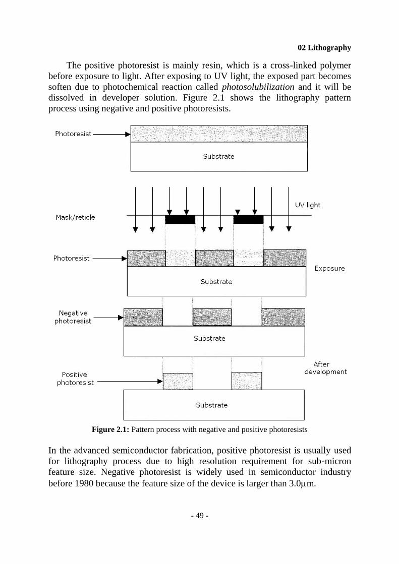
The positive photoresist is mainly resin, which is a cross-linked polymer
before exposure to light. After exposing to UV light, the exposed part becomes
soften due to photochemical reaction called photosolubilization and it will be
dissolved in developer solution. Figure 2.1 shows the lithography pattern
process using negative and positive photoresists.
Figure 2.1: Pattern process with negative and positive photoresists
In the advanced semiconductor fabrication, positive photoresist is usually used
for lithography process due to high resolution requirement for sub-micron
feature size. Negative photoresist is widely used in semiconductor industry
before 1980 because the feature size of the device is larger than 3.0m.
02 Lithography
- 50 -
Photoresist material has four components. They are polymer, sensitizer,
solvent, and additives. Let’s discuss one by one and emphasize on the
importance of each component.
2.2.1 Polymer
Polymer is an organic solid material that sticks on the surface of wafer and it
can withstand etching process and ion implantation. The polymer is an organic
compound, which is hydro-carbon CxHy with complicated chain and ring
structure. The most commonly used positive photoresist polymer is phenol-
formaldehyde or novolac resin. The most commonly used negative photoresist
polymer is polyisoprene rubber.
2.2.2 Sensitizer
The sensitizer is an organic compound with very high photosensitivity that
controls and modifies the photochemical reaction of photoresist during
exposure. The sensitizer of positive photoresist is a dissolution inhibitor, which
is cross-linked with resin. During exposure, the energy of the light dissociates
the sensitizer and breaks the cross-link of the resin and makes it soluble in
aqueous developer solution.
The sensitizer of negative photoresist is an organic molecule containing N3
group. Exposure to light will liberate nitrogen N2 gas forming free radical that
helps to cross-link the rubber molecule. The chain reaction of the cross-link
polymerizes the exposed area, which has greater bonding strength and higher
chemical resistance.
2.2.3 Solvent
Solvent is the liquid that dissolves the polymer and sensitizer and suspends
them in the liquid photoresist. It makes photoresist easy to apply on the surface
of wafer that has thickness ranges from 0.5 to 3.0m. The solvent thins the
photoresist to allow the application of thin layer by spinning. Before spin
coating, about 75% of photoresist is solvent. Solvent for positive photoresist is
commonly acetate-type solvent, while negative photoresist is xylene C8H10.
2.2.4 Additive
Additive control and modify the photochemical reaction of photoresist during
exposure to achieve optimized resolution. Dye is the common additive for both
02 Lithography
- 51 -
positive and negative photoresist that reduces reflection from the surface of
wafer that improves the resolution of the exposure.
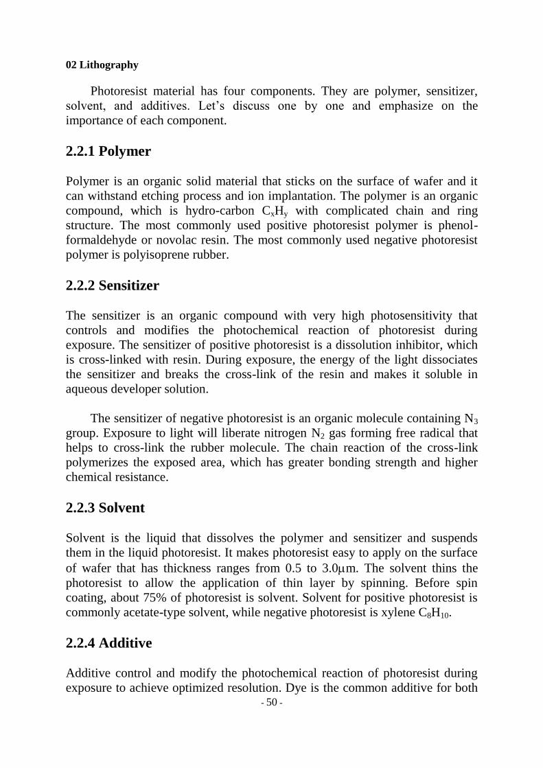
The developer solution of negative photoresist is mainly xylene. It
dissolves the unexposed uncross-linked photoresist. It causes photoresist to
swell to about three times the thickness of photoresist that affects resolution.
Positive photoresist does not absorb the developer solution. Thus, it can achieve
higher resolution. Figure 2.2 illustrates the resolution of negative and positive
photoresists.
(a) (b)
Figure 2.2: Resolution of negative and positive photoresists
To pattern small feature, short wavelength exposure light is required.
Lithography process uses deep ultra violet light with wavelength either 193nm
or 248nm. However, different wavelength requires different photoresist.
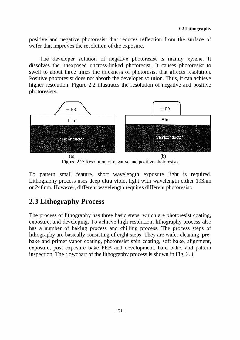
2.3 Lithography Process
The process of lithography has three basic steps, which are photoresist coating,
exposure, and developing. To achieve high resolution, lithography process also
has a number of baking process and chilling process. The process steps of
lithography are basically consisting of eight steps. They are wafer cleaning, pre-
bake and primer vapor coating, photoresist spin coating, soft bake, alignment,
exposure, post exposure bake PEB and development, hard bake, and pattern
inspection. The flowchart of the lithography process is shown in Fig. 2.3.
02 Lithography
- 52 -
Figure 2.3: Flowchart of lithography processes
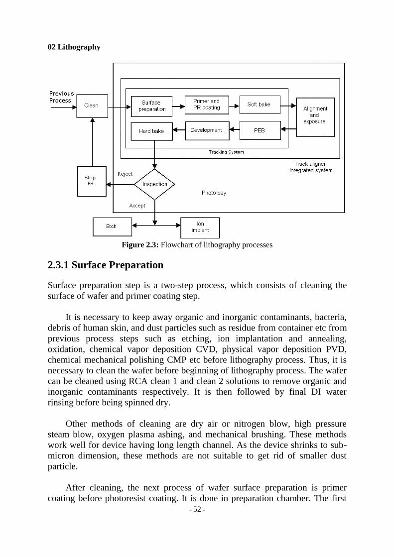
2.3.1 Surface Preparation
Surface preparation step is a two-step process, which consists of cleaning the
surface of wafer and primer coating step.
It is necessary to keep away organic and inorganic contaminants, bacteria,
debris of human skin, and dust particles such as residue from container etc from
previous process steps such as etching, ion implantation and annealing,
oxidation, chemical vapor deposition CVD, physical vapor deposition PVD,
chemical mechanical polishing CMP etc before lithography process. Thus, it is
necessary to clean the wafer before beginning of lithography process. The wafer
can be cleaned using RCA clean 1 and clean 2 solutions to remove organic and
inorganic contaminants respectively. It is then followed by final DI water
rinsing before being spinned dry.
Other methods of cleaning are dry air or nitrogen blow, high pressure
steam blow, oxygen plasma ashing, and mechanical brushing. These methods
work well for device having long length channel. As the device shrinks to sub-
micron dimension, these methods are not suitable to get rid of smaller dust
particle.
After cleaning, the next process of wafer surface preparation is primer
coating before photoresist coating. It is done in preparation chamber. The first
02 Lithography
- 53 -
step is the dehydrate bake or pre-bake process. This step is used to remove
water moisture from the surface of the wafer. This step is necessary to ensure
the surface of wafer is dry to provide good adhesion of photoresist on the
surface. Poor adhesion can lead to failure of photoresist patterning and cause
undercut during subsequent etch process. In most case, the wafer is pre-baked
for one to two minutes using a hot plate with temperature ranged from 1500C to
2000C. If the temperature and duration of pre-bake are not sufficient, dehydrated
surface may not be able to achieve optimize adhesion.
Priming process step is a process step that depositing a thin layer primer on
the surface of wafer. The purpose is to wet the surface for good adhesion of
organic photoresist with silicon surface, metallic surface, or silicon dioxide etc.
Hexamethyldisilazane HMD or (CH3)3SiNSi(CH3)3 is the most commonly used
primer. In sub-micron process, HMD is vaporized in the preparation chamber
and deposited on the surface of wafer in situ with pre-bake process. After the
process, it is important to apply photoresist coating immediately to prevent
surface dehydration. However, photoresist coating cannot be applied while the
wafer is still hot. This is because the solvent in photoresist will cool down the
hot wafer and at the same time lose due to vaporization. This makes it not
desirable for the photoresist process because there are change of viscosity of the
photoresist, the thickness of photoresist, and uniformity of the photoresist. The
hot wafer is normally chilled to ambient temperature on chilled plate, which is a
water cooled process by heat exchange on the same track system.
Primer step can be coated by spin on process in situ with photoresist
coating. But this method is not as popular as the vaporized method due to the
fact that vaporized priming will introduce less contaminant and less HMD is
used. Unlike the spin type, contaminant can be carried in liquid chemical. Spin
coating of primer is normally done by dispensing the liquid primer and spin at
low rate and then ramping up to of 3,000 to 6,000rpm for 20 to 30s to dry the
HMD.
2.3.2 Photoresist Coating
This is a process of depositing a layer of thin photoresist material on the surface
of wafer. The wafer is placed on spindle with a vacuum chuck that can hold the
wafer during the high speed rotation. Usually the thickness of photoresist
coating is between 5,000 and 30,000o
A . Photoresist has high viscosity and very
high surface tension force. Thus, high spin rate is needed. The higher the spin
rate, the thinner will be the thickness that would give better uniformity of the
photoresist layer. Photoresist thickness is inversely proportional to square root
02 Lithography
- 54 -
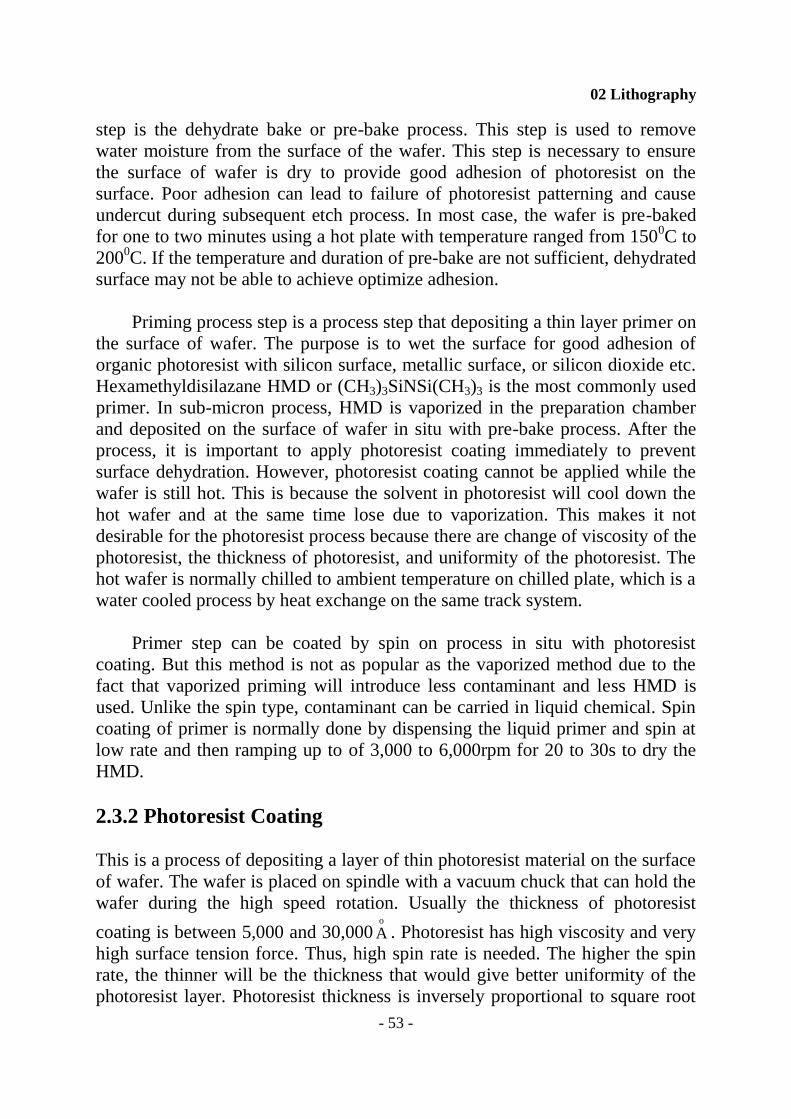
of spin rate. Figure 2.4 illustrates the thickness and its relationship with
viscosity and spin rate of wafer. It is clearly shown that the higher the spin rate,
the thinner is the thickness and also the higher the viscosity, the thicker will be
the photoresist.
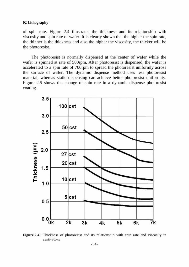
The photoresist is normally dispensed at the center of wafer while the
wafer is spinned at rate of 500rpm. After photoresist is dispensed, the wafer is
accelerated to a spin rate of 700rpm to spread the photoresist uniformly across
the surface of wafer. The dynamic dispense method uses less photoresist
material, whereas static dispensing can achieve better photoresist uniformity.
Figure 2.5 shows the change of spin rate in a dynamic dispense photoresist
coating.
Figure 2.4: Thickness of photoresist and its relationship with spin rate and viscosity in
centi-Stoke
02 Lithography
- 55 -
Figure 2.5: Spin rate of dynamic dispensing
It is important to know that once the photoresist is dispensed, it must be spinned
as quickly as possible because the solvent in photoresist is evaporating very fast
and photoresist will become viscous. In some processes, a thin layer of solvent
is spinned on surface before photoresist is spinned on to provide better adhesion
and uniformity. The dispenser also provides the feature of drawback of
photoresist to prevent the dry droplet of photoresist accumulating at the nozzle
of the dispenser due to evaporation of solvent.
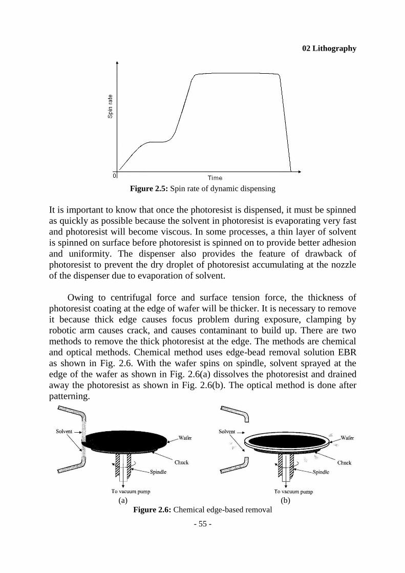
Owing to centrifugal force and surface tension force, the thickness of
photoresist coating at the edge of wafer will be thicker. It is necessary to remove
it because thick edge causes focus problem during exposure, clamping by
robotic arm causes crack, and causes contaminant to build up. There are two
methods to remove the thick photoresist at the edge. The methods are chemical
and optical methods. Chemical method uses edge-bead removal solution EBR
as shown in Fig. 2.6. With the wafer spins on spindle, solvent sprayed at the
edge of the wafer as shown in Fig. 2.6(a) dissolves the photoresist and drained
away the photoresist as shown in Fig. 2.6(b). The optical method is done after
patterning.
(a) (b)
Figure 2.6: Chemical edge-based removal
02 Lithography
- 56 -
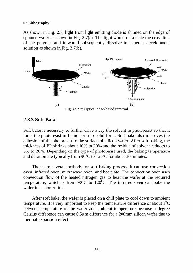
As shown in Fig. 2.7, light from light emitting diode is shinned on the edge of
spinned wafer as shown in Fig. 2.7(a). The light would dissociate the cross link
of the polymer and it would subsequently dissolve in aqueous development
solution as shown in Fig. 2.7(b).
(a) (b)
Figure 2.7: Optical edge-based removal
2.3.3 Soft Bake
Soft bake is necessary to further drive away the solvent in photoresist so that it
turns the photoresist in liquid form to solid form. Soft bake also improves the
adhesion of the photoresist to the surface of silicon wafer. After soft baking, the
thickness of PR shrinks about 10% to 20% and the residue of solvent reduces to
5% to 20%. Depending on the type of photoresist used, the baking temperature
and duration are typically from 900C to 120
0C for about 30 minutes.
There are several methods for soft baking process. It can use convection
oven, infrared oven, microwave oven, and hot plate. The convection oven uses
convection flow of the heated nitrogen gas to heat the wafer at the required
temperature, which is from 900C to 120
0C. The infrared oven can bake the
wafer in a shorter time.
After soft bake, the wafer is placed on a chill plate to cool down to ambient
temperature. It is very important to keep the temperature difference of about 10C
between temperature of the wafer and ambient temperature because a degree
Celsius difference can cause 0.5m difference for a 200mm silicon wafer due to
thermal expansion effect.
02 Lithography
- 57 -
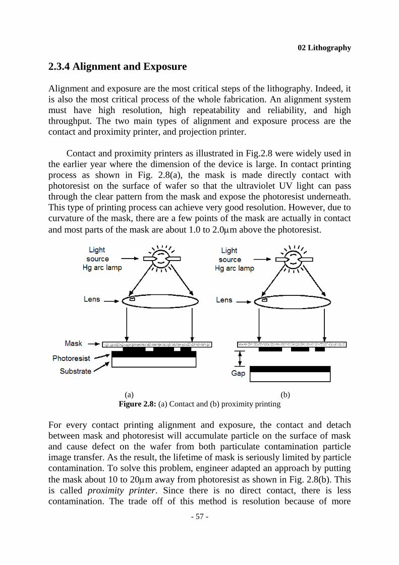
2.3.4 Alignment and Exposure
Alignment and exposure are the most critical steps of the lithography. Indeed, it
is also the most critical process of the whole fabrication. An alignment system
must have high resolution, high repeatability and reliability, and high
throughput. The two main types of alignment and exposure process are the
contact and proximity printer, and projection printer.
Contact and proximity printers as illustrated in Fig.2.8 were widely used in
the earlier year where the dimension of the device is large. In contact printing
process as shown in Fig. 2.8(a), the mask is made directly contact with
photoresist on the surface of wafer so that the ultraviolet UV light can pass
through the clear pattern from the mask and expose the photoresist underneath.
This type of printing process can achieve very good resolution. However, due to
curvature of the mask, there are a few points of the mask are actually in contact
and most parts of the mask are about 1.0 to 2.0m above the photoresist.
(a) (b)
Figure 2.8: (a) Contact and (b) proximity printing
For every contact printing alignment and exposure, the contact and detach
between mask and photoresist will accumulate particle on the surface of mask
and cause defect on the wafer from both particulate contamination particle
image transfer. As the result, the lifetime of mask is seriously limited by particle
contamination. To solve this problem, engineer adapted an approach by putting
the mask about 10 to 20m away from photoresist as shown in Fig. 2.8(b). This
is called proximity printer. Since there is no direct contact, there is less
contamination. The trade off of this method is resolution because of more
02 Lithography
- 58 -
diffraction of light. However, the best resolution can be achieved is 2m above
the photoresist. Neither contact nor proximity printers are used in today’s
VLSI/ULSI chip fabrication.
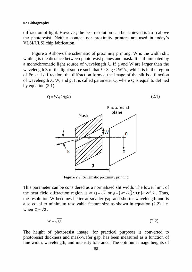
Figure 2.9 shows the schematic of proximity printing. W is the width slit,
while g is the distance between photoresist planes and mask. It is illuminated by
a monochromatic light source of wavelength . If g and W are larger than the
wavelength of the light source such that << g < W2/, which is in the region
of Fresnel diffraction, the diffraction formed the image of the slit is a function
of wavelength , W, and g. It is called parameter Q, where Q is equal to defined
by equation (2.1).
)g/(2WQ (2.1)
Figure 2.9: Schematic proximity printing
This parameter can be considered as a normalized slit width. The lower limit of
the near field diffraction region is at 2Q or /WQ/2/Wg 222 . Thus,
the resolution W becomes better at smaller gap and shorter wavelength and is
also equal to minimum resolvable feature size as shown in equation (2.2). i.e.
when 2Q .
gW (2.2)
The height of photoresist image, for practical purposes is converted to
photoresist thickness and mask-wafer gap, has been measured as a function of
line width, wavelength, and intensity tolerance. The optimum image heights of
02 Lithography
- 59 -
0.25m and 0.5m patterns are 0.9m and 3.2m respectively in the case of a
deep ultraviolet light DUV (wavelength less than about 200nm) light source
with ±5% intensity tolerance.
Another parameter is the divergence of the illuminating beam as a result of
the size of the light source. One effect is to smooth out the undulations in the
image intensity profile, and the other is to produce a greater line width variation
as the mask-to-wafer distance varies. The apparent source size of the
illumination system must be large enough to give a value of that allows the
smallest features to be printed. The mercury arc lamp used as the source is too
small to yield the required wavelength . The illumination is telecentric or
normally incident at the mask to prevent run-out (magnification) error similar to
that in X-ray lithography. The optical system must also minimize non-
uniformity of the intensity across the field. The illumination system needs to
have a large enough and normal incidence. With a mercury arc source, the
strong lines at G-line 436nm, H-line 405nm, and I-line 365nm. It can provide
the exposure sufficient flux. The same printer is available with a xenon mercury
Xe-Hg source for enhanced output in the 200-300nm spectral regions.
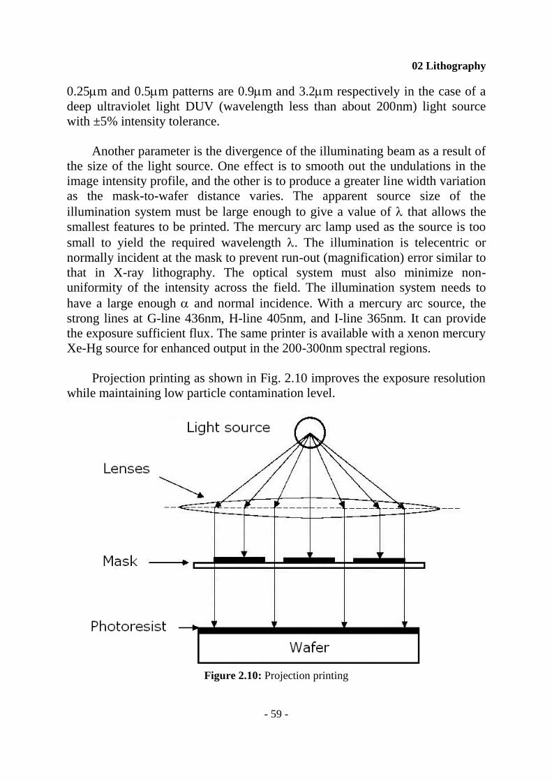
Projection printing as shown in Fig. 2.10 improves the exposure resolution
while maintaining low particle contamination level.
Figure 2.10: Projection printing
02 Lithography
- 60 -
Projection exposure system was developed and became widely used in VLSI
semiconductor device fabrication. It has a larger separation between the mask
and the wafer because of its image formation system. According to Rayleigh's
criterion, the resolution W of the optical system is given by in equation (2.3).
NA/kW 1 (2.3)
k1 is equal to 0.6. It is used to account for process type and numerical aperture
NA of the lens.
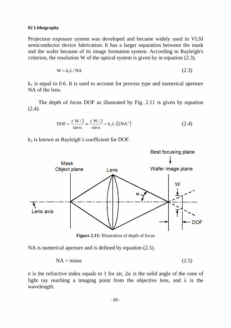
The depth of focus DOF as illustrated by Fig. 2.11 is given by equation
(2.4).
2
2 NA2/ksin
2/W
tan
2/WDOF
(2.4)
k2 is known as Rayleigh’s coefficient for DOF.
Figure 2.11: Illustration of depth of focus
NA is numerical aperture and is defined by equation (2.5).
NA = nsin (2.5)
n is the refractive index equals to 1 for air, 2 is the solid angle of the cone of
light ray reaching a imaging point from the objective lens, and is the
wavelength.
02 Lithography
- 61 -
It is believed that high numerical aperture NA is always better. However,
in the submicron region there is an optimum numerical aperture NA if a
resolution requirement and imaging wavelength are given. If the numerical
aperture is too low, the resolution cannot be achieved. If the numerical aperture
is too high, the depth of focus DOF, which inversely proportional to (NA)2,
becomes unacceptable. The optimum NA at which DOF is at maximum. the
normalization of the resolution W derived from equation (2.3) is given by
NA
Wk1 (2.6)
where k1 is known as Rayleigh’s coefficient for resolution but is now redefined
as the normalized resolution. Thus, the normalized DOF is given by
2
2
)NA(Zk (2.7)
where Z is the physical axial displacement from the focal plane and k2 is
known as Rayleigh’s coefficient for DOF, is now defined as the normalized
DOF.
Projection printing works like an overhead projector. The mask is like the
transparency foil and the image is refocused on the surface in 1:1 ratio. This
type of printing can achieve 1.0m minimum feature size. This is because of the
optical characteristics of lens and mirror. This type of system is widely used in
the VLSI device fabrication.
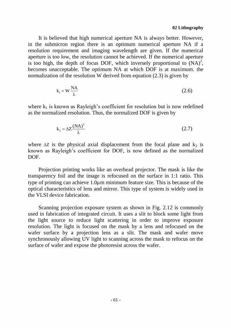
Scanning projection exposure system as shown in Fig. 2.12 is commonly
used in fabrication of integrated circuit. It uses a slit to block some light from
the light source to reduce light scattering in order to improve exposure
resolution. The light is focused on the mask by a lens and refocused on the
wafer surface by a projection lens as a slit. The mask and wafer move
synchronously allowing UV light to scanning across the mask to refocus on the
surface of wafer and expose the photoresist across the wafer.
02 Lithography
- 62 -
Figure 2.12: Scanning projection printing
When the feature size continues to shrink and approaches sub-micron level, the
projection system no longer can meet the requirement of resolution. A different
approach of exposure is needed. The step and repeat system as shown in Fig.
2.13 has to be used especially for VLSI/ULSI fabrication.
In the normal exposure system, the image transfer is 1:1 ratio and the wafer
needs only one exposure for transferring the pattern from the mask to
photoresist. The step and repeat system shrinks the image of mask/reticle and
refocuses it on the photoresist at the ratio of 5:1 or 10:1. In this manner the
resolution of pattern transfer can be improved. However, in this type of
exposure system, it is not possible to expose the whole wafer in one exposure.
The reason being, it is not possible to make a mask that is 5X or 10X of the size
of wafer, it is not possible to get a high precise optical system that can shrink
the pattern of such a large mask/reticle, and finally, there is no UV light
intensity that is high enough to provide the exposure of whole wafer. Therefore,
for this system type, the mask/reticle is made larger than the size of an
integrated circuit and the exposure is not the whole wafer surface. The exposure
is made on a particular part of the wafer that has image of reticle. Thus, one
needs to repeat the step and exposure multiple times until the whole wafer is
exposed. Thus, a step and repeat exposure system has xy table whereby it can
precisely control the step and followed by exposure. The stepper system is a
02 Lithography
- 63 -
complicated system. It needs alignment for every step. Each wafer requires 20
to 60 steps to complete the exposure.
(a) An example of 10:1 (b) An example of 5:1
Figure 2.13: Step and repeat exposure printing
For step and exposure system used in sub-micron device fabrication, there is no
room for error. Also in order to meet the throughput requirement, each exposure
step takes one to two seconds to complete. Thus, an automatic alignment system
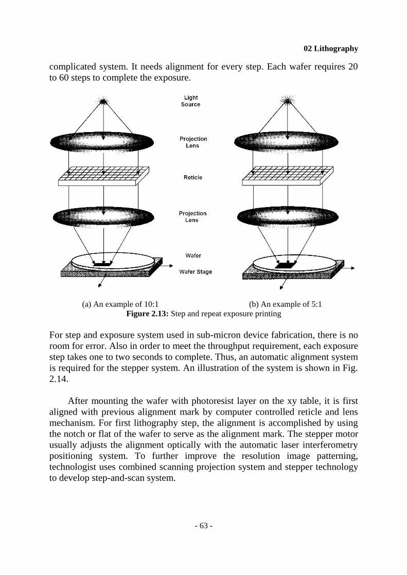
is required for the stepper system. An illustration of the system is shown in Fig.
2.14.
After mounting the wafer with photoresist layer on the xy table, it is first
aligned with previous alignment mark by computer controlled reticle and lens
mechanism. For first lithography step, the alignment is accomplished by using
the notch or flat of the wafer to serve as the alignment mark. The stepper motor
usually adjusts the alignment optically with the automatic laser interferometry
positioning system. To further improve the resolution image patterning,
technologist uses combined scanning projection system and stepper technology
to develop step-and-scan system.
02 Lithography
- 64 -
Figure 2.14: A step and repeat alignment and exposure automatic system
A photographer knows that he/she needs high light intensity in order he/she can
capture high resolution picture. Besides, it would take longer exposure time in
low light intensity environment than high light intensity environment. Thus,
high intensity light is a key to have high resolution and high throughput. The
ultra violet UV light source used in the exposure system is the key for a
successful exposure. The wavelength of UV light is also a key factor because
the sensitivity of photoresist is dependent on wavelength. Moreover, the feature
size of the device is also dependent on wavelength of the light source. As the
device shrinks down, the wavelength of the UV light has to be shorter to match
the requirement of the pattern resolution.
There are two types of light source that are widely used for lithography
process. They are mercury light and excimer laser. Exposure light source must
be stable, reliable, and adjustable, with short wavelength, high intensity, and
long lifetime. For feature size greater than 2.0m, the broad band mercury lamp
is used as light source for contact/proximity and projection printing. When the
feature size shrinks, single wavelength light source is required to achieve the
desired resolution. High pressure mercury arc lamp is the most commonly used
light source to get ultraviolet UV for sub-micron lithography projection system
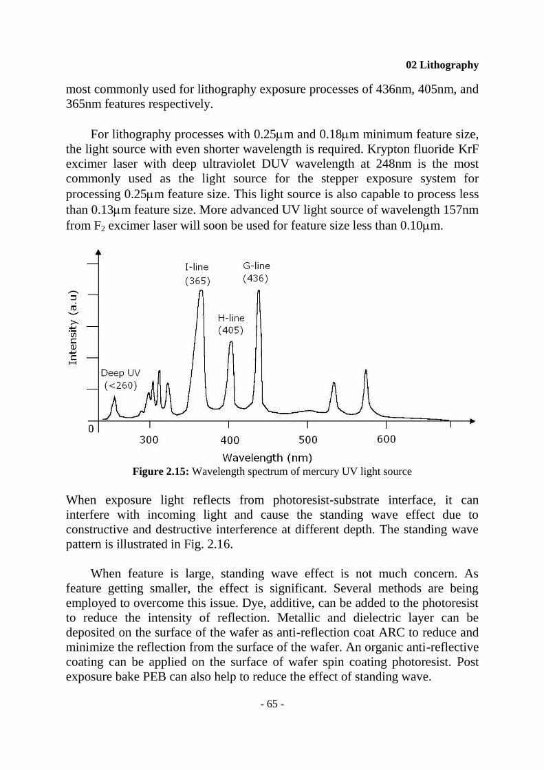
and stepper system used in the 80’s and 90’s. The wavelength spectrum mercury
ultraviolet light source is shown in Fig. 2.15. The G-line, H-line, I-line are the
02 Lithography
- 65 -
most commonly used for lithography exposure processes of 436nm, 405nm, and
365nm features respectively.
For lithography processes with 0.25m and 0.18m minimum feature size,
the light source with even shorter wavelength is required. Krypton fluoride KrF
excimer laser with deep ultraviolet DUV wavelength at 248nm is the most
commonly used as the light source for the stepper exposure system for
processing 0.25m feature size. This light source is also capable to process less
than 0.13m feature size. More advanced UV light source of wavelength 157nm
from F2 excimer laser will soon be used for feature size less than 0.10m.
Figure 2.15: Wavelength spectrum of mercury UV light source
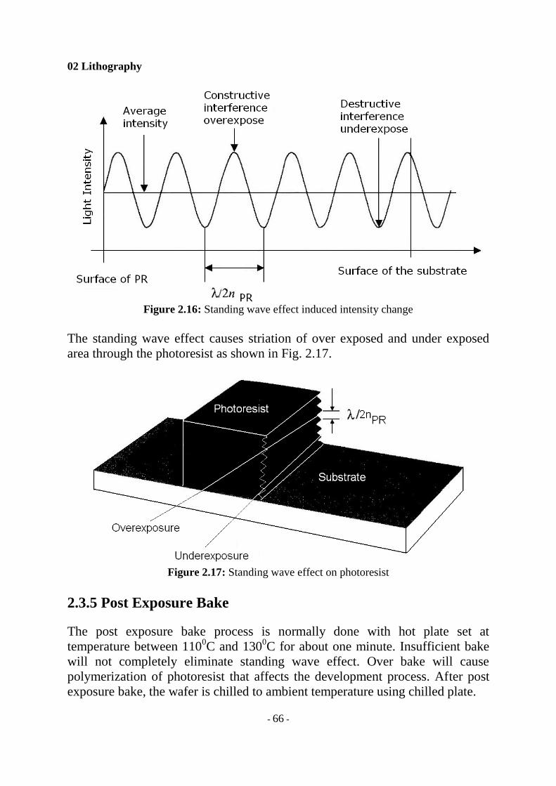
When exposure light reflects from photoresist-substrate interface, it can
interfere with incoming light and cause the standing wave effect due to
constructive and destructive interference at different depth. The standing wave
pattern is illustrated in Fig. 2.16.
When feature is large, standing wave effect is not much concern. As
feature getting smaller, the effect is significant. Several methods are being
employed to overcome this issue. Dye, additive, can be added to the photoresist
to reduce the intensity of reflection. Metallic and dielectric layer can be
deposited on the surface of the wafer as anti-reflection coat ARC to reduce and
minimize the reflection from the surface of the wafer. An organic anti-reflective
coating can be applied on the surface of wafer spin coating photoresist. Post
exposure bake PEB can also help to reduce the effect of standing wave.
02 Lithography
- 66 -
Figure 2.16: Standing wave effect induced intensity change
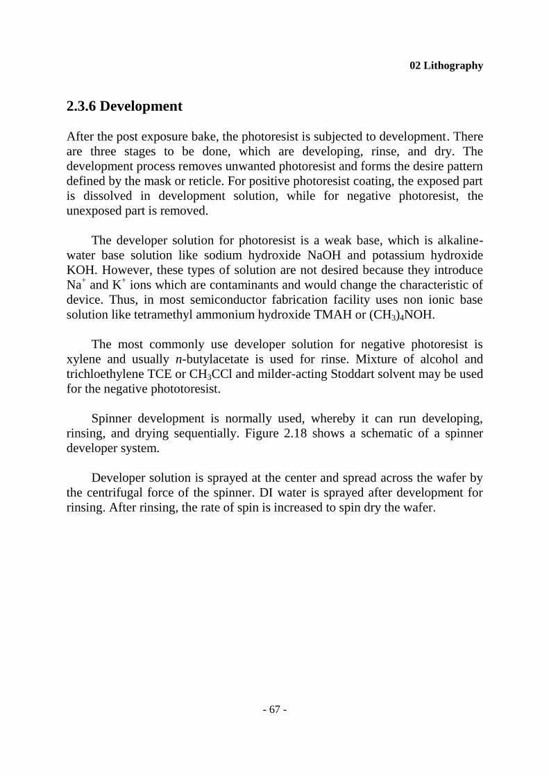
The standing wave effect causes striation of over exposed and under exposed
area through the photoresist as shown in Fig. 2.17.
Figure 2.17: Standing wave effect on photoresist
2.3.5 Post Exposure Bake
The post exposure bake process is normally done with hot plate set at
temperature between 1100C and 130
0C for about one minute. Insufficient bake
will not completely eliminate standing wave effect. Over bake will cause
polymerization of photoresist that affects the development process. After post
exposure bake, the wafer is chilled to ambient temperature using chilled plate.
02 Lithography
- 67 -
2.3.6 Development
After the post exposure bake, the photoresist is subjected to development. There
are three stages to be done, which are developing, rinse, and dry. The
development process removes unwanted photoresist and forms the desire pattern
defined by the mask or reticle. For positive photoresist coating, the exposed part
is dissolved in development solution, while for negative photoresist, the
unexposed part is removed.
The developer solution for photoresist is a weak base, which is alkaline-
water base solution like sodium hydroxide NaOH and potassium hydroxide
KOH. However, these types of solution are not desired because they introduce
Na+ and K
+ ions which are contaminants and would change the characteristic of
device. Thus, in most semiconductor fabrication facility uses non ionic base
solution like tetramethyl ammonium hydroxide TMAH or (CH3)4NOH.
The most commonly use developer solution for negative photoresist is
xylene and usually n-butylacetate is used for rinse. Mixture of alcohol and
trichloethylene TCE or CH3CCl and milder-acting Stoddart solvent may be used
for the negative phototoresist.
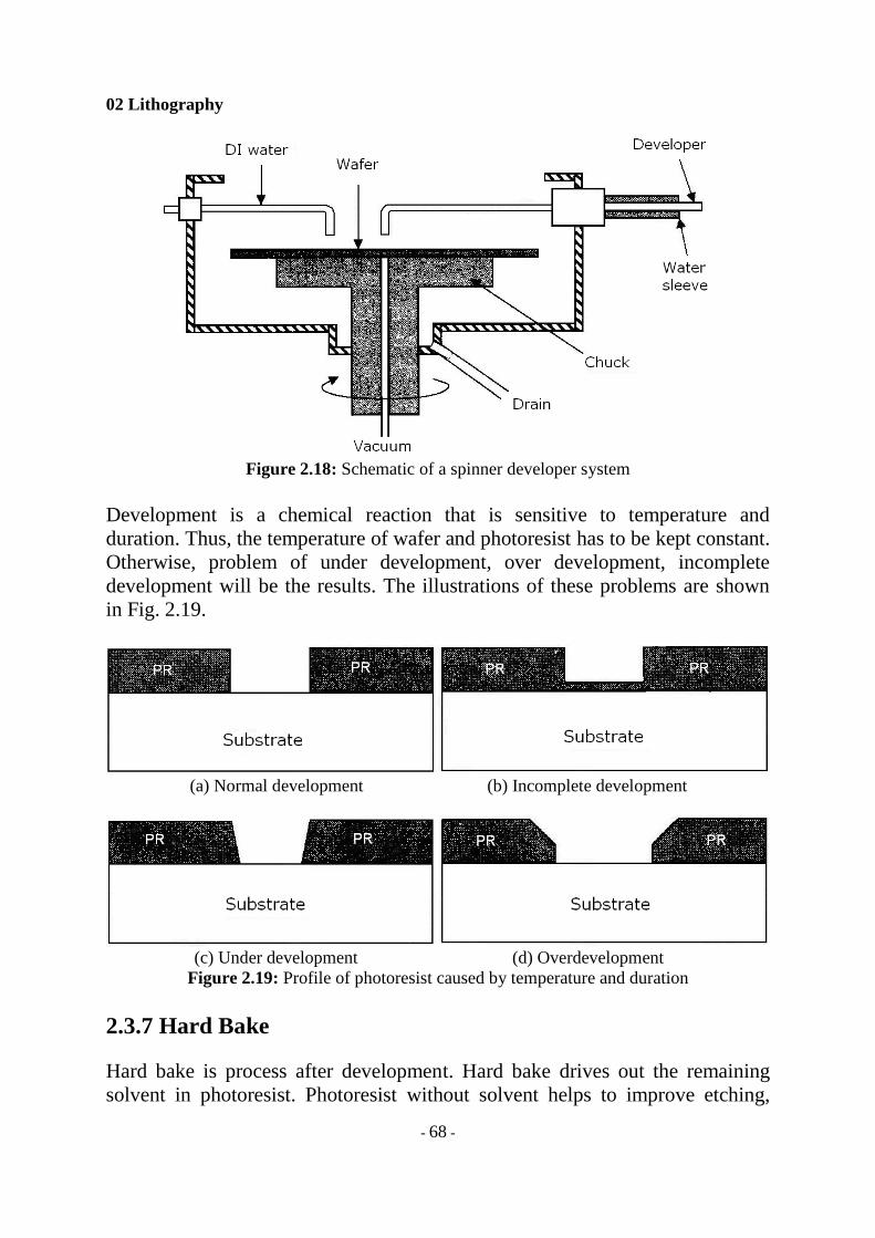
Spinner development is normally used, whereby it can run developing,
rinsing, and drying sequentially. Figure 2.18 shows a schematic of a spinner
developer system.
Developer solution is sprayed at the center and spread across the wafer by
the centrifugal force of the spinner. DI water is sprayed after development for
rinsing. After rinsing, the rate of spin is increased to spin dry the wafer.
02 Lithography
- 68 -
Figure 2.18: Schematic of a spinner developer system
Development is a chemical reaction that is sensitive to temperature and
duration. Thus, the temperature of wafer and photoresist has to be kept constant.
Otherwise, problem of under development, over development, incomplete
development will be the results. The illustrations of these problems are shown
in Fig. 2.19.
(a) Normal development (b) Incomplete development
(c) Under development (d) Overdevelopment
Figure 2.19: Profile of photoresist caused by temperature and duration
2.3.7 Hard Bake
Hard bake is process after development. Hard bake drives out the remaining
solvent in photoresist. Photoresist without solvent helps to improve etching,
02 Lithography
- 69 -
adhesion to surface of wafer, and resistance to ion implantation due to more
polymerization.
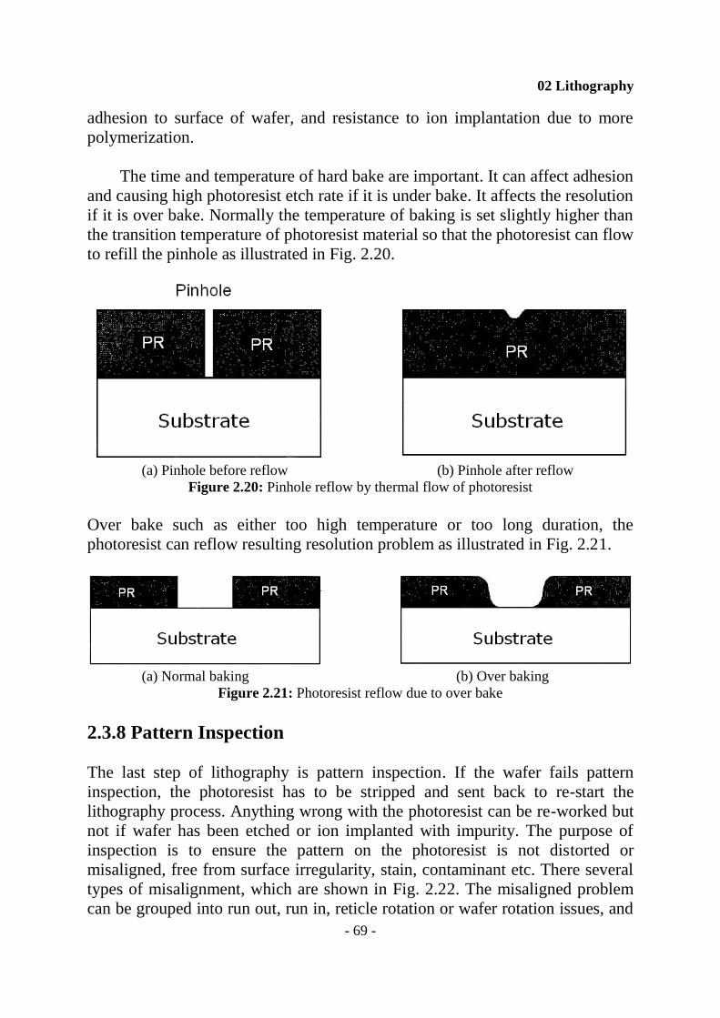
The time and temperature of hard bake are important. It can affect adhesion
and causing high photoresist etch rate if it is under bake. It affects the resolution
if it is over bake. Normally the temperature of baking is set slightly higher than
the transition temperature of photoresist material so that the photoresist can flow
to refill the pinhole as illustrated in Fig. 2.20.
(a) Pinhole before reflow (b) Pinhole after reflow
Figure 2.20: Pinhole reflow by thermal flow of photoresist
Over bake such as either too high temperature or too long duration, the
photoresist can reflow resulting resolution problem as illustrated in Fig. 2.21.
(a) Normal baking (b) Over baking
Figure 2.21: Photoresist reflow due to over bake
2.3.8 Pattern Inspection
The last step of lithography is pattern inspection. If the wafer fails pattern
inspection, the photoresist has to be stripped and sent back to re-start the
lithography process. Anything wrong with the photoresist can be re-worked but
not if wafer has been etched or ion implanted with impurity. The purpose of
inspection is to ensure the pattern on the photoresist is not distorted or
misaligned, free from surface irregularity, stain, contaminant etc. There several
types of misalignment, which are shown in Fig. 2.22. The misaligned problem
can be grouped into run out, run in, reticle rotation or wafer rotation issues, and
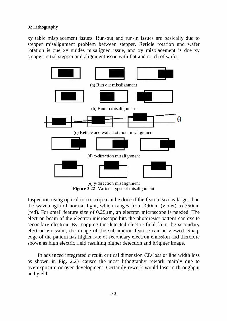
02 Lithography
- 70 -
xy table misplacement issues. Run-out and run-in issues are basically due to
stepper misalignment problem between stepper. Reticle rotation and wafer
rotation is due xy guides misaligned issue, and xy misplacement is due xy
stepper initial stepper and alignment issue with flat and notch of wafer.
(a) Run out misalignment
(b) Run in misalignment
(c) Reticle and wafer rotation misalignment
(d) x-direction misalignment
(e) y-direction misalignment
Figure 2.22: Various types of misalignment
Inspection using optical microscope can be done if the feature size is larger than
the wavelength of normal light, which ranges from 390nm (violet) to 750nm
(red). For small feature size of 0.25m, an electron microscope is needed. The
electron beam of the electron microscope hits the photoresist pattern can excite
secondary electron. By mapping the detected electric field from the secondary
electron emission, the image of the sub-micron feature can be viewed. Sharp
edge of the pattern has higher rate of secondary electron emission and therefore
shown as high electric field resulting higher detection and brighter image.
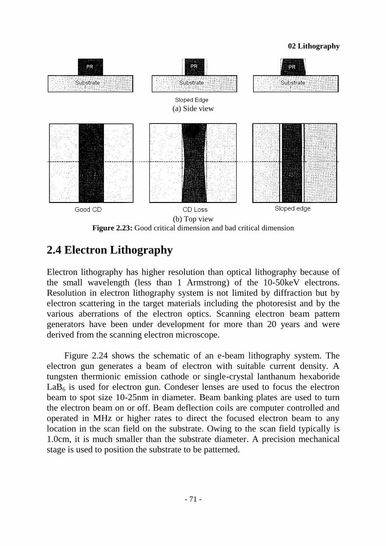
In advanced integrated circuit, critical dimension CD loss or line width loss
as shown in Fig. 2.23 causes the most lithography rework mainly due to
overexposure or over development. Certainly rework would lose in throughput
and yield.
02 Lithography
- 71 -
(a) Side view
(b) Top view
Figure 2.23: Good critical dimension and bad critical dimension
2.4 Electron Lithography
Electron lithography has higher resolution than optical lithography because of
the small wavelength (less than 1 Armstrong) of the 10-50keV electrons.
Resolution in electron lithography system is not limited by diffraction but by
electron scattering in the target materials including the photoresist and by the
various aberrations of the electron optics. Scanning electron beam pattern
generators have been under development for more than 20 years and were
derived from the scanning electron microscope.
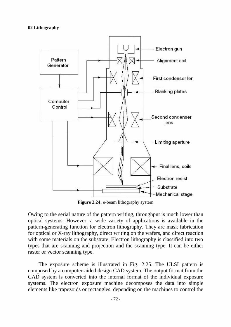
Figure 2.24 shows the schematic of an e-beam lithography system. The
electron gun generates a beam of electron with suitable current density. A
tungsten thermionic emission cathode or single-crystal lanthanum hexaboride
LaB6 is used for electron gun. Condeser lenses are used to focus the electron
beam to spot size 10-25nm in diameter. Beam banking plates are used to turn
the electron beam on or off. Beam deflection coils are computer controlled and
operated in MHz or higher rates to direct the focused electron beam to any
location in the scan field on the substrate. Owing to the scan field typically is
1.0cm, it is much smaller than the substrate diameter. A precision mechanical
stage is used to position the substrate to be patterned.
02 Lithography
- 72 -
Figure 2.24: e-beam lithography system
Owing to the serial nature of the pattern writing, throughput is much lower than
optical systems. However, a wide variety of applications is available in the
pattern-generating function for electron lithography. They are mask fabrication
for optical or X-ray lithography, direct writing on the wafers, and direct reaction
with some materials on the substrate. Electron lithography is classified into two
types that are scanning and projection and the scanning type. It can be either
raster or vector scanning type.
The exposure scheme is illustrated in Fig. 2.25. The ULSI pattern is
composed by a computer-aided design CAD system. The output format from the
CAD system is converted into the internal format of the individual exposure
systems. The electron exposure machine decomposes the data into simple
elements like trapezoids or rectangles, depending on the machines to control the
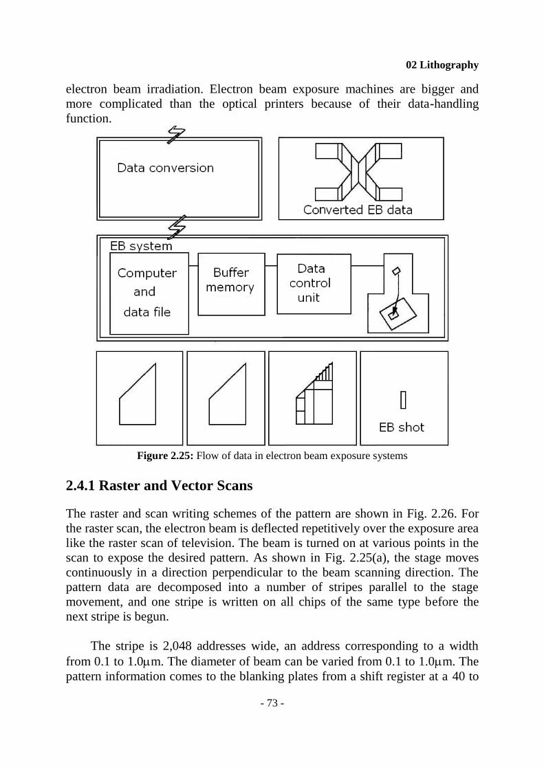
02 Lithography
- 73 -
electron beam irradiation. Electron beam exposure machines are bigger and
more complicated than the optical printers because of their data-handling
function.
Figure 2.25: Flow of data in electron beam exposure systems
2.4.1 Raster and Vector Scans
The raster and scan writing schemes of the pattern are shown in Fig. 2.26. For
the raster scan, the electron beam is deflected repetitively over the exposure area
like the raster scan of television. The beam is turned on at various points in the
scan to expose the desired pattern. As shown in Fig. 2.25(a), the stage moves
continuously in a direction perpendicular to the beam scanning direction. The
pattern data are decomposed into a number of stripes parallel to the stage
movement, and one stripe is written on all chips of the same type before the
next stripe is begun.
The stripe is 2,048 addresses wide, an address corresponding to a width
from 0.1 to 1.0m. The diameter of beam can be varied from 0.1 to 1.0m. The
pattern information comes to the blanking plates from a shift register at a 40 to
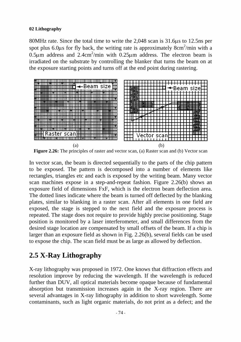
02 Lithography
- 74 -
80MHz rate. Since the total time to write the 2,048 scan is 31.6s to 12.5ns per
spot plus 6.0s for fly back, the writing rate is approximately 8cm2/min with a
0.5m address and 2.4cm2/min with 0.25m address. The electron beam is
irradiated on the substrate by controlling the blanker that turns the beam on at
the exposure starting points and turns off at the end point during rastering.
(a) (b)
Figure 2.26: The principles of raster and vector scan, (a) Raster scan and (b) Vector scan
In vector scan, the beam is directed sequentially to the parts of the chip pattern
to be exposed. The pattern is decomposed into a number of elements like
rectangles, triangles etc and each is exposed by the writing beam. Many vector
scan machines expose in a step-and-repeat fashion. Figure 2.26(b) shows an
exposure field of dimensions FxF, which is the electron beam deflection area.
The dotted lines indicate where the beam is turned off deflected by the blanking
plates, similar to blanking in a raster scan. After all elements in one field are
exposed, the stage is stepped to the next field and the exposure process is
repeated. The stage does not require to provide highly precise positioning. Stage
position is monitored by a laser interferometer, and small differences from the
desired stage location are compensated by small offsets of the beam. If a chip is
larger than an exposure field as shown in Fig. 2.26(b), several fields can be used
to expose the chip. The scan field must be as large as allowed by deflection.
2.5 X-Ray Lithography
X-ray lithography was proposed in 1972. One knows that diffraction effects and
resolution improve by reducing the wavelength. If the wavelength is reduced
further than DUV, all optical materials become opaque because of fundamental
absorption but transmission increases again in the X-ray region. There are
several advantages in X-ray lithography in addition to short wavelength. Some
contaminants, such as light organic materials, do not print as a defect; and the
02 Lithography
- 75 -
depth of focus is larger than the optical printers. The essential technology
components of this process are (1) a mask consisting of a device pattern made
of X-ray absorbing materials on transmitting material, (2) an X-ray source, and
(3) an X-ray resist.
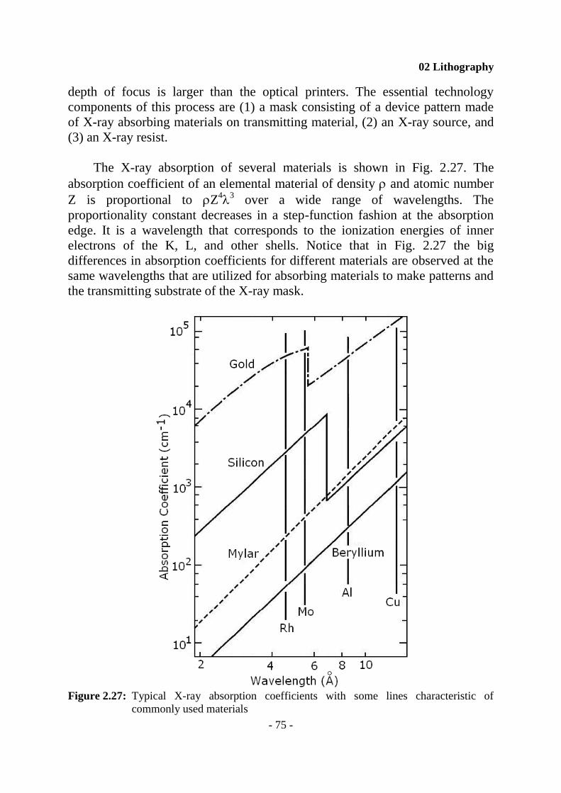
The X-ray absorption of several materials is shown in Fig. 2.27. The
absorption coefficient of an elemental material of density and atomic number
Z is proportional to Z4
3 over a wide range of wavelengths. The
proportionality constant decreases in a step-function fashion at the absorption
edge. It is a wavelength that corresponds to the ionization energies of inner
electrons of the K, L, and other shells. Notice that in Fig. 2.27 the big
differences in absorption coefficients for different materials are observed at the
same wavelengths that are utilized for absorbing materials to make patterns and
the transmitting substrate of the X-ray mask.
Figure 2.27: Typical X-ray absorption coefficients with some lines characteristic of
commonly used materials
02 Lithography
- 76 -
The performance required of X-ray lithography, as the alternative to optical
lithography, has become more exacting as optical technology has continued to
improve. The resolution and placement accuracy should surpass 0.2m and
0.03m respectively.
2.5.1 Proximity Printing
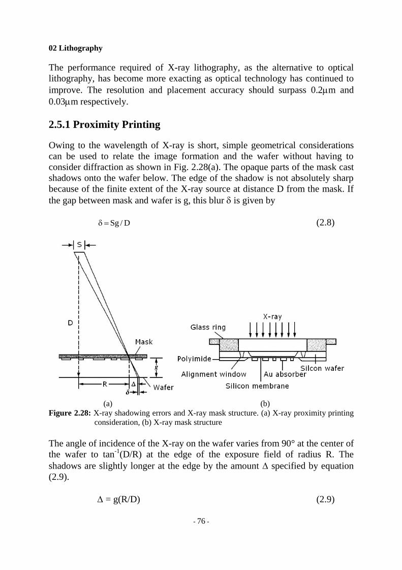
Owing to the wavelength of X-ray is short, simple geometrical considerations
can be used to relate the image formation and the wafer without having to
consider diffraction as shown in Fig. 2.28(a). The opaque parts of the mask cast
shadows onto the wafer below. The edge of the shadow is not absolutely sharp
because of the finite extent of the X-ray source at distance D from the mask. If
the gap between mask and wafer is g, this blur is given by
D/Sg (2.8)
(a) (b)
Figure 2.28: X-ray shadowing errors and X-ray mask structure. (a) X-ray proximity printing
consideration, (b) X-ray mask structure
The angle of incidence of the X-ray on the wafer varies from 90° at the center of
the wafer to tan-1
(D/R) at the edge of the exposure field of radius R. The
shadows are slightly longer at the edge by the amount specified by equation
(2.9).
= g(R/D) (2.9)
02 Lithography
- 77 -
This small magnification is generally of no concern. In the special case where it
may be undesirable but it can be compensated for when the mask is patterned.
For multi-level devices the magnification must have the same value for each
level or at least its variation must be within the registration tolerance. This
implies stringent control of the gap g. Wafer warping in processing can be
nearly eliminated with a proper vacuum chuck. It is not necessary that the gaps
have the same value at all points on the wafer, only that the spatial variations be
the same, within close tolerance, for all levels. The step-and-repeat motion is
indispensable to the narrow beam line of X-ray lithography.
2.5.2 X-Ray Mask
The role of an X-ray mask is to select where the impinging radiation is allowed
to reach the resist and where it is not allowed. An example of a typical mask
structure is shown in Fig. 2.28(b). An X-ray mask consists of a transmissive
membrane substrate, which is usually made of low atomic number material like
beryllium, carbon (amorphous or glassy graphite) and a patterned absorber
layer, in which it is usually made of heavy metal such as gold. The ratio of
metal thickness to substrate thickness is greater than for a photo mask because
no material is available that is fully transparent or fully absorbent, unlike the
combination of glass and chromium in optical lithography. This thickness is
determined by the transmission of the materials for the X-ray wavelength of
interest. X-ray masks are made by electron lithography and use the technologies
of mask making and direct writing. The pattern on the X-ray mask must be as
perfect as a photo mask, but the dimension is the same as on the wafer because
of proximity printing. For features down to 0.1 to 0.2m geometry it is harder to
check the pattern integrity and to repair defects in X-ray than in optical
lithography.
Of the heavy metals with large Z4 values, gold was once widely used,
because it is relatively easily patterned by liftoff or electroplating. Tungsten and
tantalum are used now, because they are easily etched by dry etching. The
thicknesses of gold necessary for absorption of 90% of the incident X-ray flux
are 0.7m, 0.5m, 0.2m, and 0.08m for X-ray wavelengths 4.4o
A (PdL), 8.3o
A
(A1K), 13.3o
A (CuL), or 44.8o
A (CK) respectively. In general, the metal is
considerably thicker than the chromium layer (0.1m) on a photo mask.
Methods for high resolution patterning of the gold include electroplating and
ion milling. Electroplating produces excellent definition with vertical walls but
requires a vertical wall primary pattern in a resist that has a thickness equal to
that of the metal to be plated. More often, a subtractive process has been
02 Lithography
- 78 -
employed in which a thinner resist layer is used to pattern a thin layer of a
refractive metal; the refractive metal serves as a mask for ion-milling the
underlying gold. With this method, walls that depart from the vertical by 20° or
less can be formed. The minimum line width attainable by ion milling 0.5m
thick gold is approximately 0.4m For higher resolution, and where gold
thickness can be reduced, longer wavelengths such as the 12o
A CuL radiation
may be used. Line as small as 0.16m, has been replicated with this type of
radiation.
The membrane forming the mask substrate should be as transparent as
possible to the X-rays, smooth, flat, dimensionally stable, reasonably rugged,
and transparent to visible light if an optical registration scheme is used.
Materials that have been used include polymers such as polyimide and
polyethylene terephthalate, silicon, silicon carbide SiC, silicon nitride Si3N4,
Al2O3, and a Si3N4-SiO2-Si3N4 sandwich structure. Although different mask
substrates are appropriate for different portions of the soft X-ray spectrum, there
is not yet general agreement on the best material for any particular wavelength.
The major questions remaining about X-ray masks concern their
dimensional stability, minimum attainable defect densities, and ease of
handling. The stress applied on the thin membrane during processing and
formation of the absorber structure causes distortions. Absorber-induced
distortion is not noticeable because it is evaluated by comparing the measured
fiducial marks before and after electroplating. Resist films on the membrane
produce tensile stress on the membrane. In the case of a multilayer process, RIE
heating can cause membrane distortion with a maximum error of 0.1m.
Dimensional stability can be degraded by radiation damage produced by x-ray
flux, which also makes the mask substrate optically opaque. Pattern placement
and critical dimension CD accuracies are reported as 0.06m (3) and are
repeatable.
2.6 Ion Lithography
Ion beam used to expose a resist has possible higher resolution than with an
electron beam because of less scattering. In addition, resists are more sensitive
to ions than to electrons. There is also the possibility of a resistless wafer
process. However, the most important application of ion lithography is the
repair of masks for optical or X-ray lithography, which is available commercial
systems.
02 Lithography
- 79 -
The sputtering yield increases with beam energy if the beam energy is
larger than some small threshold value. However, there is an energy limit
beyond which the yield decreases because the ions penetrate more deeply and
fewer surface atoms receive enough energy to leave the surface. For example,
the peak in the sputtering curve for Ar+ ions incident on copper Cu occurs at
23.0keV. For ion implantation, energies from 30.0keV to 500.0keV are used,
and the dose ranges up to 1015
ions/cm2 (or 1.6x10
-4C/cm
2 for monovalent ions).
This represents a much larger dose than that used for resist exposure.
The sensitivity of polymethyl methacrylate PMMA resist has been
measured for 30.0keV, 60.0keV, and 200.0keV He+ ions and for 100.0keV and
150.0keV Ar+ ions. The required dose is nearly two orders of magnitude less
than with 20.0keV electrons. The perpendicular straggle of the penetrating ion
path and the range of low-energy secondary electrons produced are less than the
range of backscattered electrons in electron lithography. The ion energies for
exposing a resist depend on the ion species. If the ion must penetrate 2,500o
A of
resist, then a proton would need 14.0keV; and a gold Au ion, 600.0keV for the
projected range to be 3,000o
A .
Two types of ion lithography systems are available, which are scanning
focused-beam system and a mask-beam system. The problems of ion optics for
scanning ion systems are more serious than for electron optics. The problems
are the ion source and the beam-forming system.
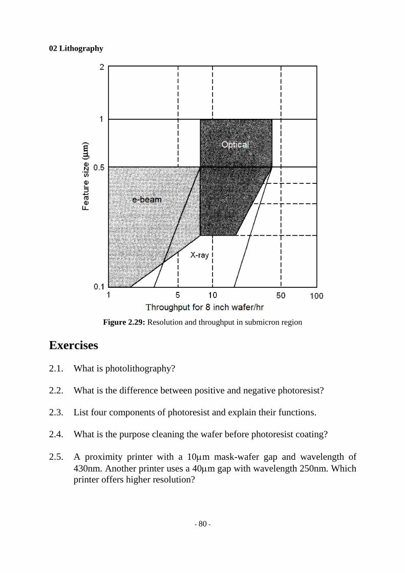
The performance of various lithography methods based on throughput and
resolution are summarized in Fig. 2.29. The borderline of each technology is
very fuzzy. It will be difficult for another technology to replace optical
lithography until 0.2µm resolution is required. However, other key issues are
the pattern-width uniformity and the overlay accuracy. If the tolerances of these
items are defined as 10% of the feature size, they should be less than 0.02µm. It
is very difficult to guarantee these accuracies because the accuracy of present
measurement tools cannot meet this requirement. Pattern-geometry accuracy is
degraded in each step of the device manufacturing process.
02 Lithography
- 80 -
Figure 2.29: Resolution and throughput in submicron region
Exercises
2.1. What is photolithography?
2.2. What is the difference between positive and negative photoresist?
2.3. List four components of photoresist and explain their functions.
2.4. What is the purpose cleaning the wafer before photoresist coating?
2.5. A proximity printer with a 10m mask-wafer gap and wavelength of
430nm. Another printer uses a 40m gap with wavelength 250nm. Which
printer offers higher resolution?
02 Lithography
- 81 -
2.6. Why must the reticle used in a wafer stepper be completely free of
defect? Why some defects can be tolerated in system exposing the entire
wafer at once?
2.7. What is the purpose of post exposure baking?
2.8. List the consequences of overbaking and underbaking.
2.9. Explain the purpose of post exposure bake. What can go wrong from
overbaking and underbaking of PEB?
2.10. Why does the wafer need inspection before next process step after
lithography?
2.11. Most likely optical lithography cannot be used for nano-device that
minimum feature size less than 50nm patterning process. State the reason.
02 Lithography
- 82 -
Bibliography
1. Hong Xiao, “Introduction to Semiconductor Manufacturing Technology”,
Pearson Prentice Hall, 2001.
2. SM Sze, “VLSI Technology”, second edition, McGraw-Hill, 1988.
3. CY Chang and SM Sze, “ULSI Technology”, McGraw-Hill, 1996.
4. Cary S. May and Costas J. Spanos, “Fundamentals of Semiconductor
Manufacturing and Process Control”, Wiley-Interscience, 2006.
5. Stefan Landis, “Nano Lithography”, ISTE-Wiley, 2010.
Index
- 83 -
A
Absorption coefficient ......................................... 75 Alumina ................................................................ 78 Anti-refection coat ............................................... 65 Argon ................................................................... 79 Atomic number .................................................... 75
B
Beryllium .............................................................. 77
C
CAD system .......................................................... 72 Carbon ................................................................. 77 Chemical mechanical polishing ............................ 52 Chemical vapor deposition ............................ 47, 52 Chromium ...................................................... 48, 77 Computer-aided design ....................................... 72 Contact printer .................................................... 57 Copper ................................................................. 79 Critical dimension .......................................... 70, 78
D
Deep ultraviolet light ..................................... 59, 65 Depth of focus ............................................... 60, 61 Development ....................................................... 67 DOF ............................................ See Depth of Focus DUV ................................. See Deep untraviolet light
E
e-beam lithography ............................................. 71 Edge-bead removal .............................................. 55 Electron lithography ...................................... 71, 72 Excimer laser ........................................................ 64
F
F2 excimer laser ................................................... 65 Fresnel diffraction ................................................ 58
G
Gold ............................................................... 77, 79
H
Hard bake ............................................................ 68 Hexamethyldisilazane .......................................... 53 HMD ................................ See Hexamethyldisilazane
I
Integrated circuit ................................................. 47 Ion implantation .................................................. 47 Ion lithography .................................................... 78
K
KeF excimer laser ................................................. 65
Krypton fluoride ................................................... 65
L
LaB6 .............................. See Lanthanum hexaboride Lanthanum hexaboride ........................................ 71 Laser interferometry ............................................ 63 Lithography .......................................................... 47
Electron lithography................................... 71, 78 Optical lithography ........................ 71, 76, 77, 79 UV light lithography ......................................... 57 X-ray lithography .............................................. 74
M
Mask ..................................................................... 47 Mercury light........................................................ 64 Metal deposition .................................................. 47
N
n-butylacetate ...................................................... 67 Nitrogen ............................................................... 50 Numerical aperture .............................................. 60
P
Pattern inspection ................................................ 69 Phenol-formaldehyde .......................................... 50 Photoresist ................................... 47, 48, 49, 56, 68
Negative type ................................................... 49 Positive type ..................................................... 49
Photosolubilization .............................................. 49 Physical vapor deposition .................................... 52 PMMA ....................... See Polymethyl methacrylate Polycrystalline process ......................................... 47 Polyethylene ........................................................ 78 Polyimide ............................................................. 78 Polyisoprene ........................................................ 50 Polymer ................................................................ 50 Polymethyl methacrylate ..................................... 79 Post exposure bake .................................. 51, 65, 66 Potassium hydroxide ............................................ 67 Project printing .................................................... 61 Proximity printer ............................................ 57, 76
R
Raster scan ........................................................... 73 Rayleigh’s coefficient ........................................... 61 Rayleigh's criterion ............................................... 60 RCA clean 1 solution ............................................ 52 RCA clean 2 solution ............................................ 52 Reactive ion epitaxy ............................................. 78 Refractive index ................................................... 60 Reticle .................................................................. 48
S
Silicon carbide ...................................................... 78
02 Lithography
- 84 -
Silicon dioxide ...................................................... 47 Silicon nitride ................................................. 47, 78 Sintering ............................................................... 47 Sodium hydroxide ................................................ 67 Soft bake .............................................................. 56 Standing wave effect ........................................... 66 Stepper system .................................................... 62 Stoddart solution ................................................. 67
T
Terephthalate ...................................................... 78 Tetramethyl ammonium hydroxide ..................... 67 Thin film process .................................................. 47 Titanium nitride ................................................... 47 Titanium silicide ................................................... 47 Titanium-tungsten alloy ....................................... 47 TMAH .........See Tetramethyl ammonium hydroxide Trichloethylene .................................................... 67 Tungsten silicide .................................................. 47
U
ULSI ....................... See Ultra large scale integration Ultra large scale integration............... 47, 58, 62, 72 Ultraviolet light ........................................ 48, 49, 64
V
Vector scan .......................................................... 74 Very large scale integration ............... 47, 58, 60, 62 Viscosity ............................................................... 53 VLSI ......................... See Very large scale integraion
X
Xenon mercury ..................................................... 59 X-ray ..................................................................... 47 X-ray lithography................................ 72, 74, 77, 78 X-ray mask ............................................................ 77 Xylene .................................................................. 50