Introduction to PLLs - · PDF file1 Introduction to PLLs Behzad Razavi Electrical Engineering...
30
1 Introduction to PLLs Behzad Razavi Electrical Engineering Department University of California, Los Angeles
Transcript of Introduction to PLLs - · PDF file1 Introduction to PLLs Behzad Razavi Electrical Engineering...
1
Introduction to PLLs
Behzad RazaviElectrical Engineering Department
University of California, Los Angeles
2
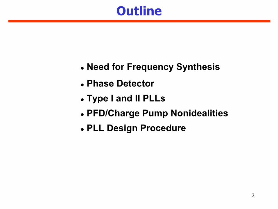
Outline
Need for Frequency Synthesis
Phase DetectorType I and II PLLsPFD/Charge Pump NonidealitiesPLL Design Procedure
3
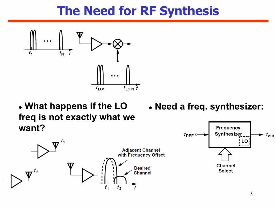
The Need for RF Synthesis
What happens if the LO freq is not exactly what we want?
Need a freq. synthesizer:
4
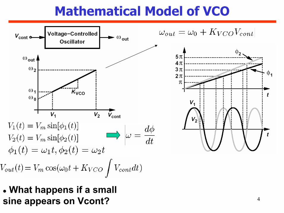
Mathematical Model of VCO
What happens if a small sine appears on Vcont?
5
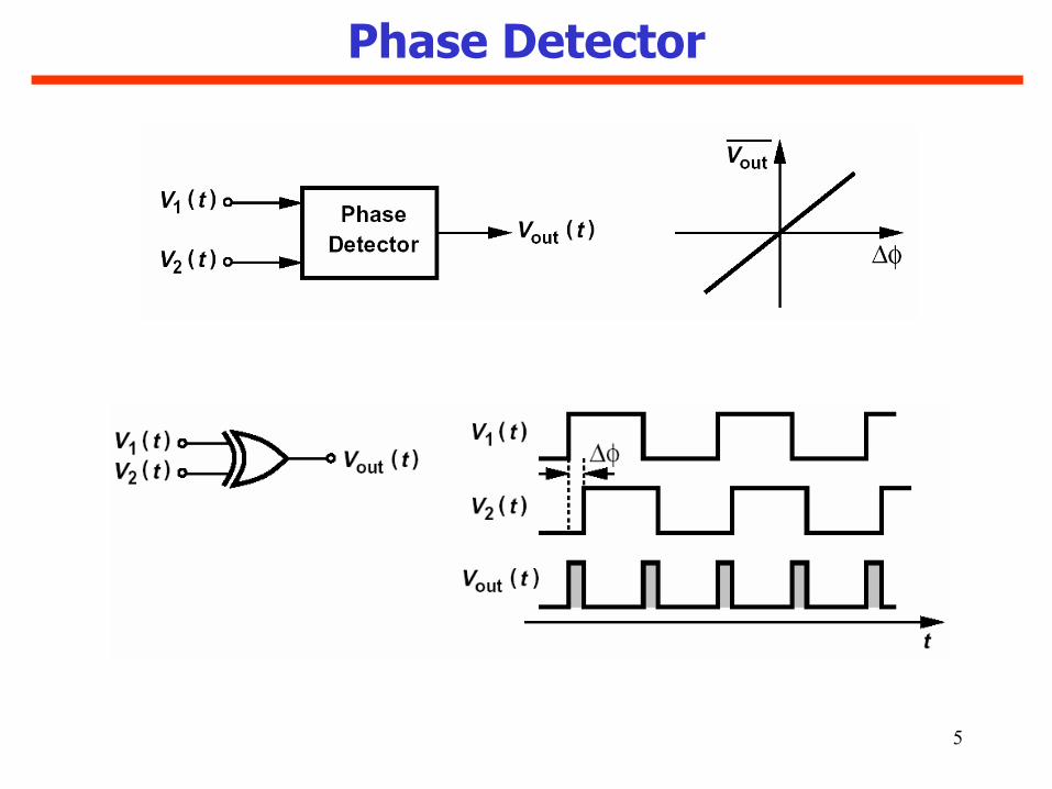
Phase Detector
6
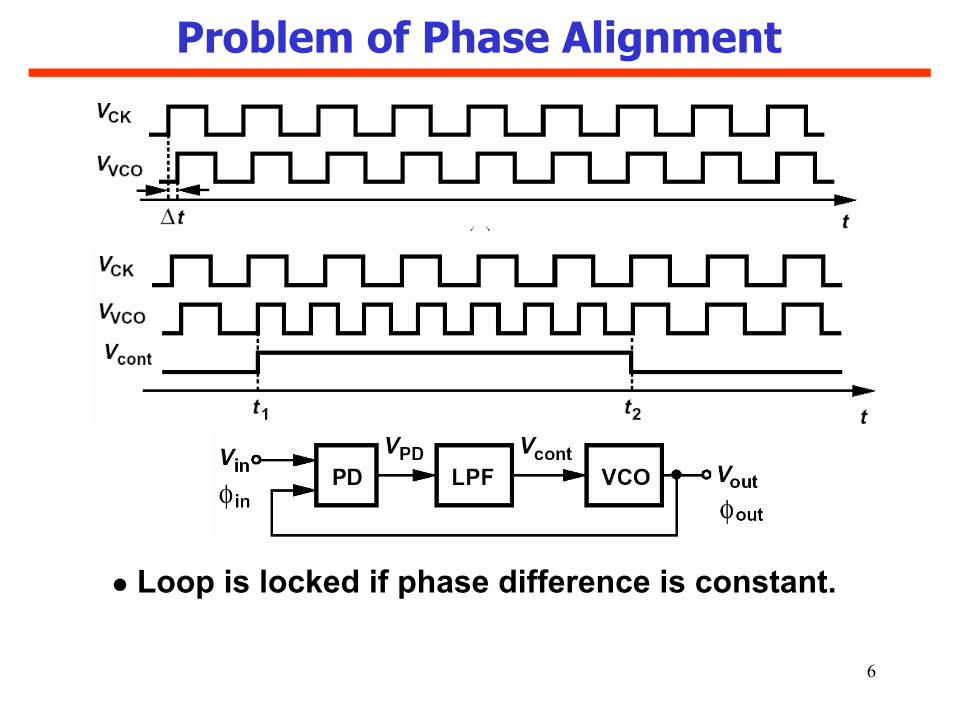
Problem of Phase Alignment
Loop is locked if phase difference is constant.
7
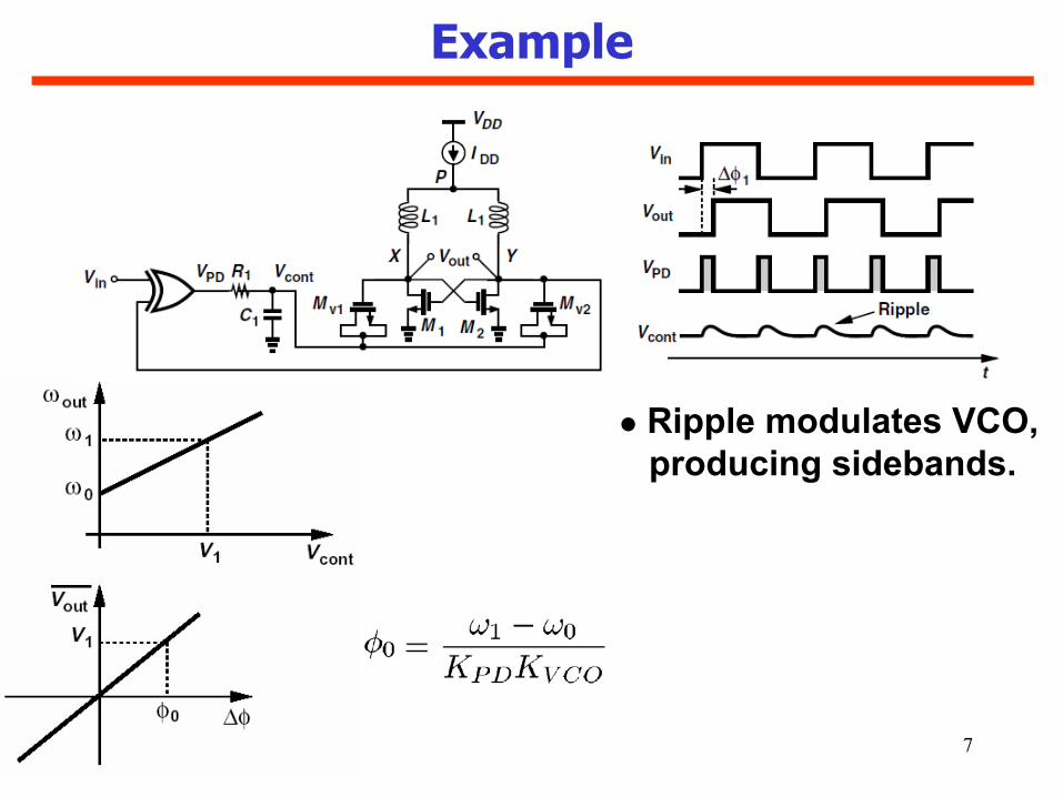
Example
Ripple modulates VCO, producing sidebands.
8
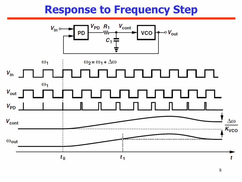
Response to Frequency Step
9
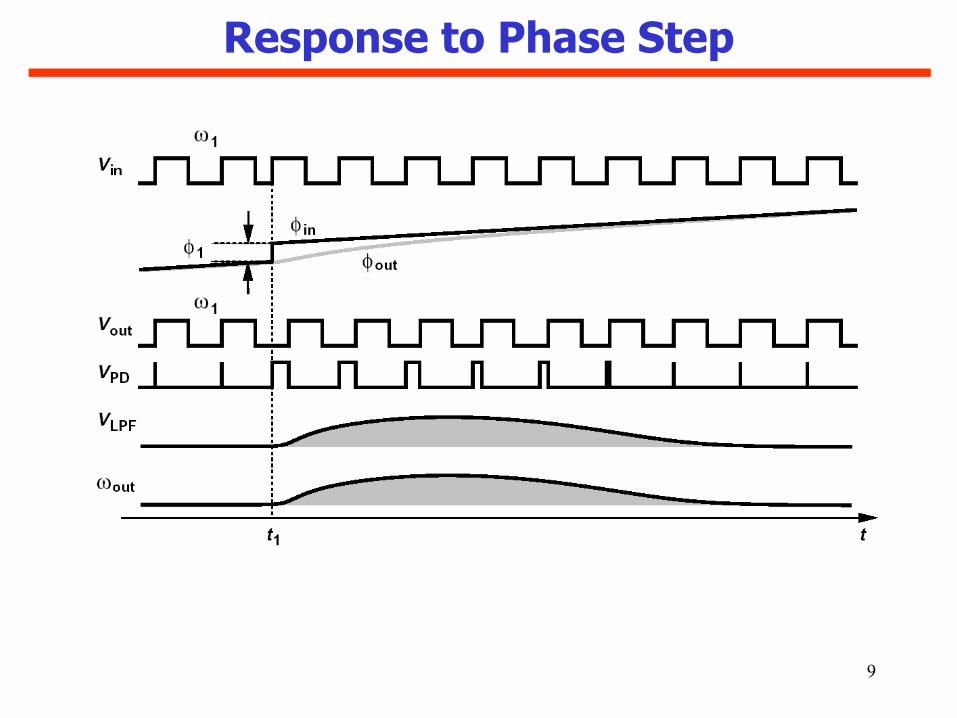
Response to Phase Step
10
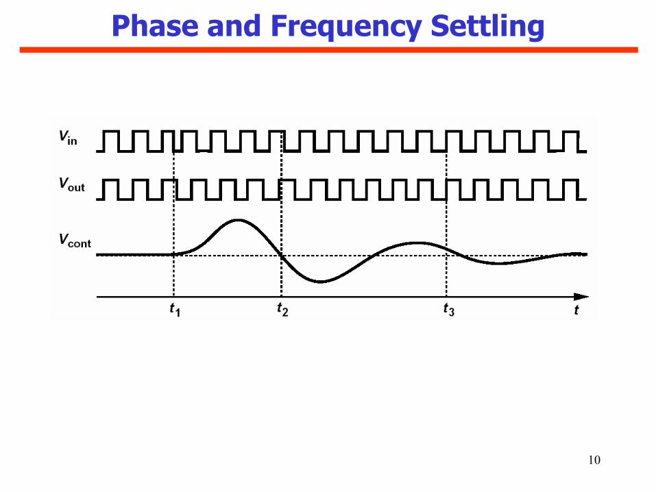
Phase and Frequency Settling
11
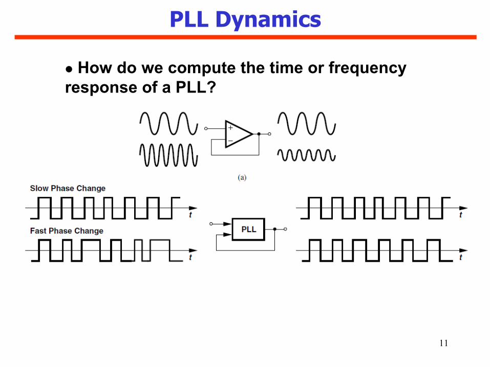
PLL Dynamics
How do we compute the time or frequency response of a PLL?
12
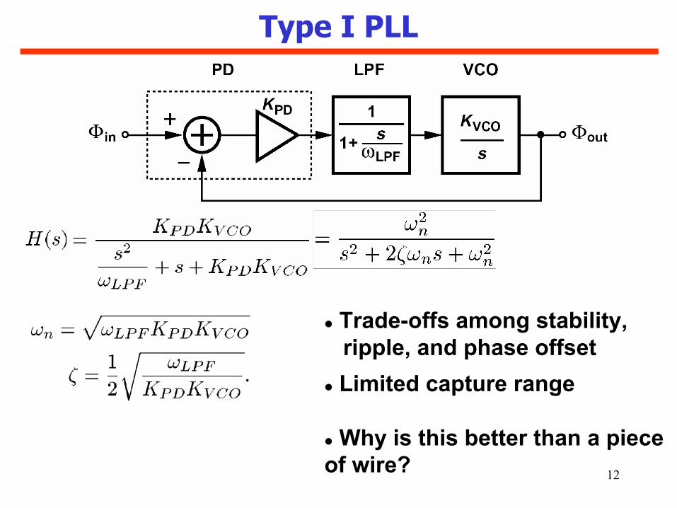
Type I PLL
Trade-offs among stability,ripple, and phase offsetLimited capture range
Why is this better than a piece of wire?
13
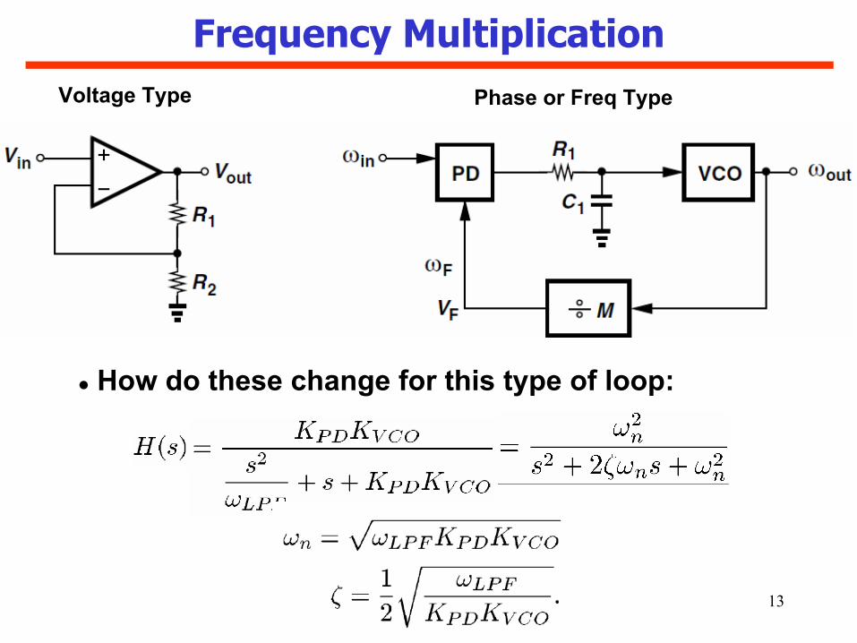
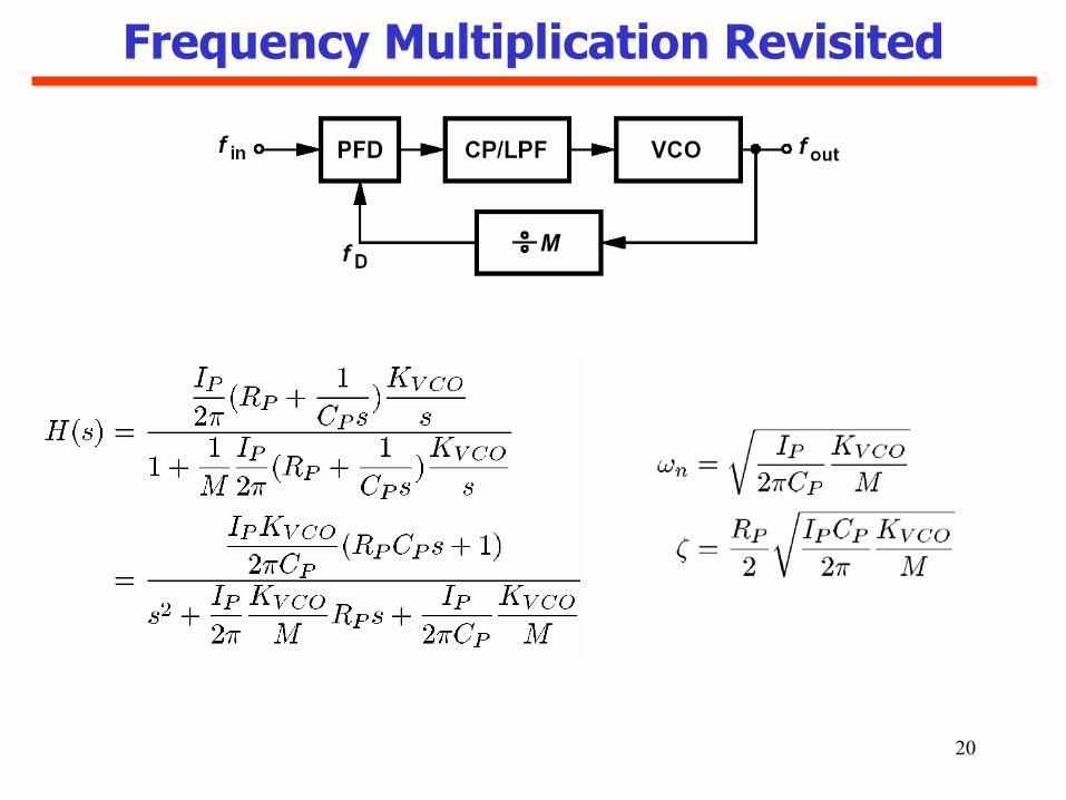
Frequency MultiplicationVoltage Type Phase or Freq Type
How do these change for this type of loop:
14
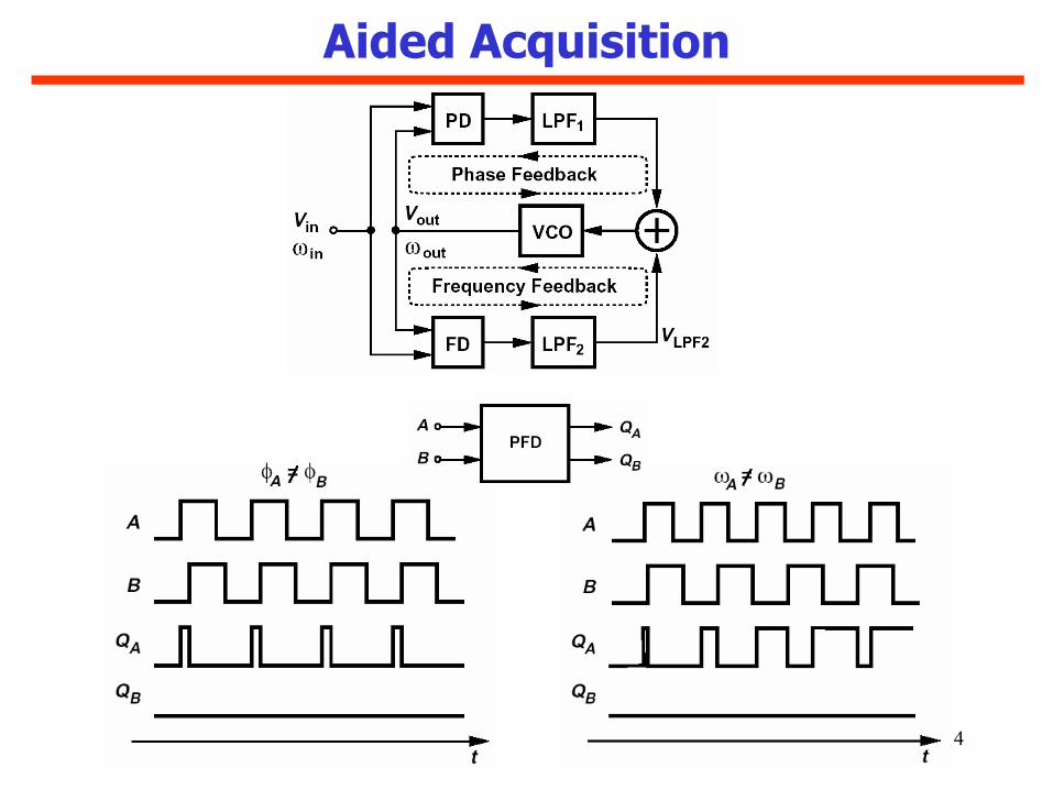
Aided Acquisition
15
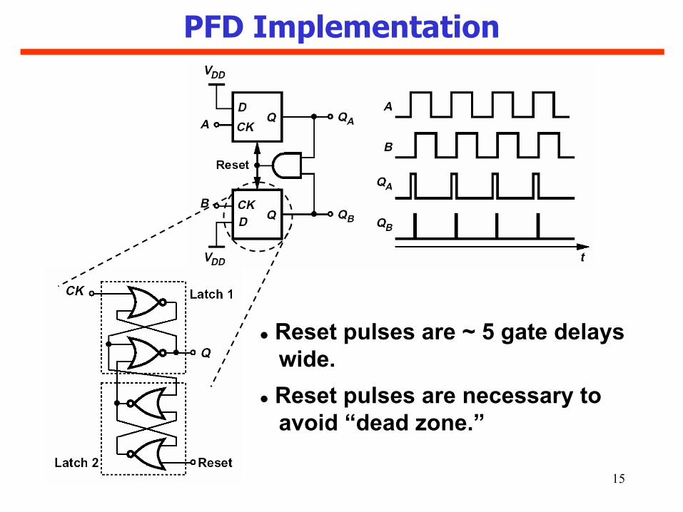
PFD Implementation
Reset pulses are ~ 5 gate delays wide.Reset pulses are necessary to avoid “dead zone.”
16
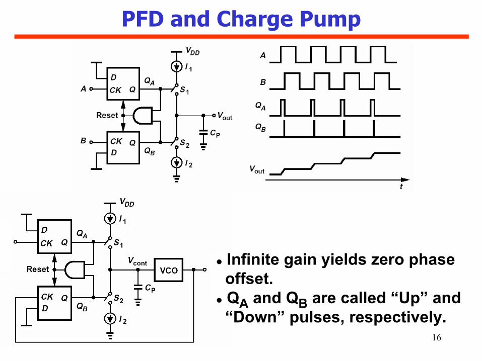
PFD and Charge Pump
Infinite gain yields zero phase offset.QA and QB are called “Up” and “Down” pulses, respectively.
17
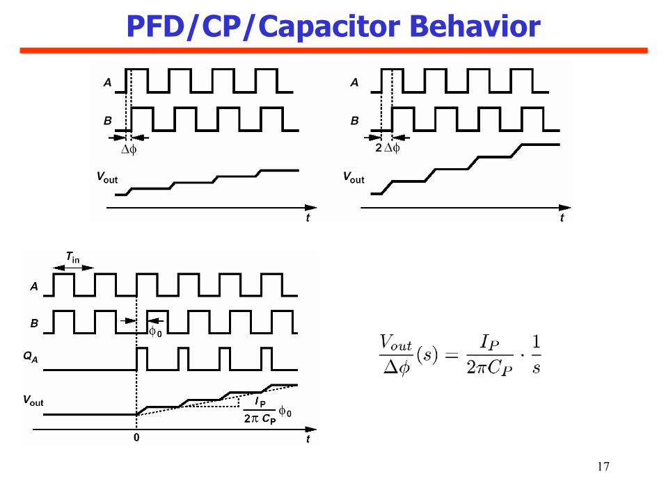
PFD/CP/Capacitor Behavior
18
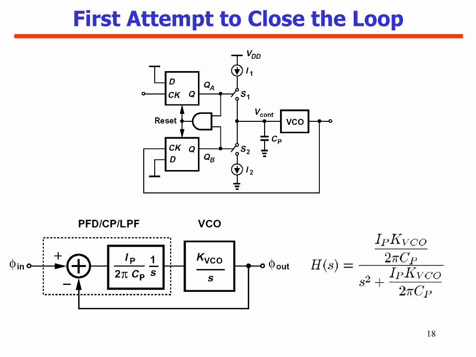
First Attempt to Close the Loop
19
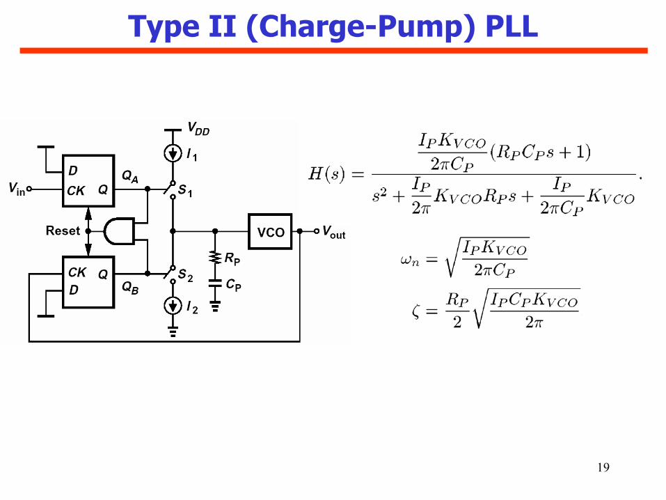
Type II (Charge-Pump) PLL
20
Frequency Multiplication Revisited
21
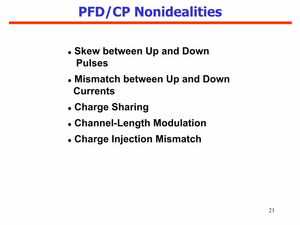
PFD/CP Nonidealities
Skew between Up and Down PulsesMismatch between Up and DownCurrentsCharge SharingChannel-Length ModulationCharge Injection Mismatch
22
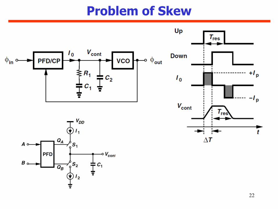
Problem of Skew
23
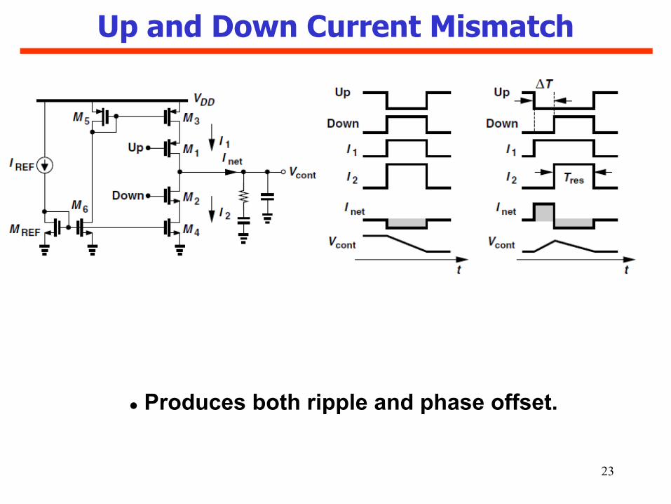
Up and Down Current Mismatch
Produces both ripple and phase offset.
24
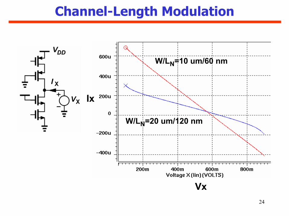
Channel-Length Modulation
Ix
Vx
W/LN=10 um/60 nm
W/LN=20 um/120 nm
25
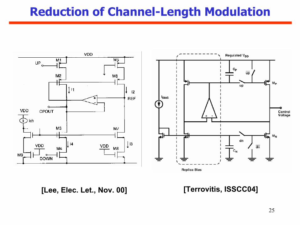
Reduction of Channel-Length Modulation
[Lee, Elec. Let., Nov. 00] [Terrovitis, ISSCC04]
26
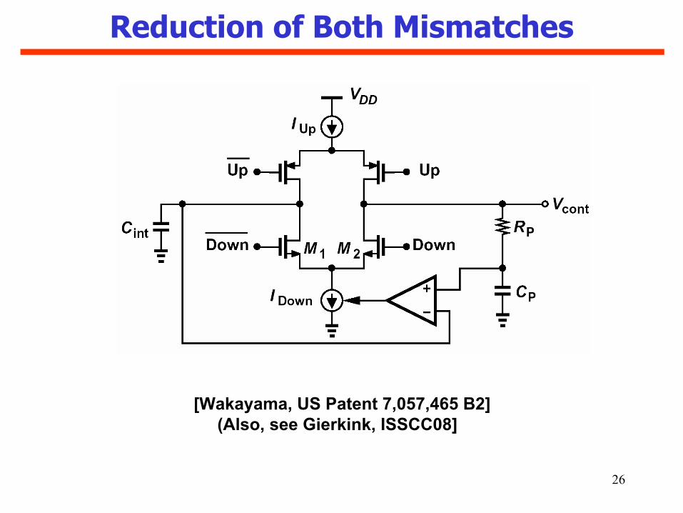
Reduction of Both Mismatches
[Wakayama, US Patent 7,057,465 B2](Also, see Gierkink, ISSCC08]
27
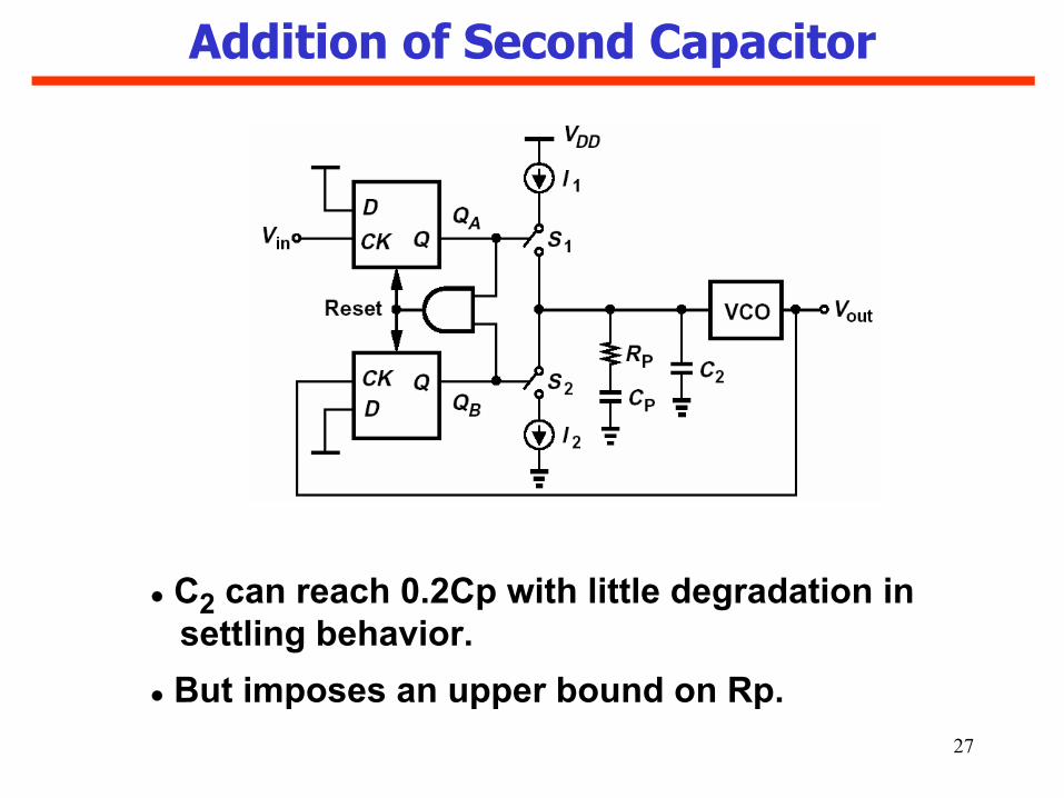
Addition of Second Capacitor
C2 can reach 0.2Cp with little degradation in settling behavior.But imposes an upper bound on Rp.
28
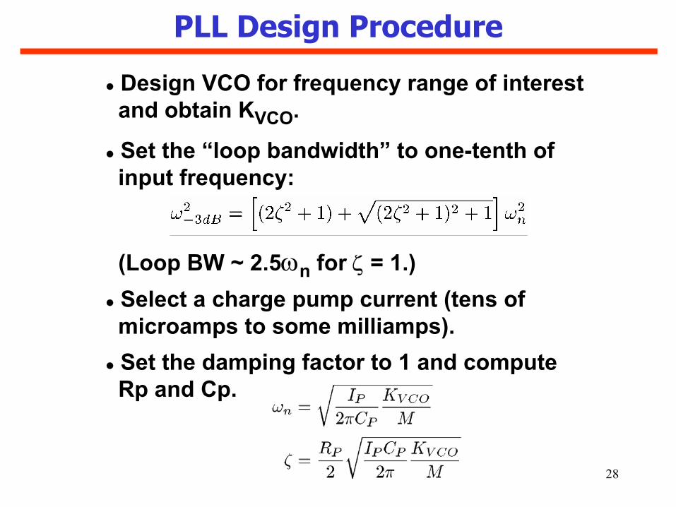
PLL Design Procedure
Design VCO for frequency range of interest and obtain KVCO.
Set the “loop bandwidth” to one-tenth of input frequency:
(Loop BW ~ 2.5ωn for ζ = 1.)Select a charge pump current (tens of microamps to some milliamps).Set the damping factor to 1 and computeRp and Cp.
29
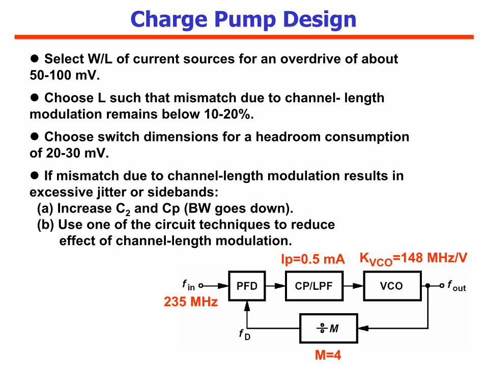
Charge Pump Design
Select W/L of current sources for an overdrive of about 50-100 mV.
Choose L such that mismatch due to channel- length modulation remains below 10-20%.
Choose switch dimensions for a headroom consumption of 20-30 mV.
If mismatch due to channel-length modulation results in excessive jitter or sidebands:(a) Increase C2 and Cp (BW goes down).(b) Use one of the circuit techniques to reduce
effect of channel-length modulation.
M=4
KVCO=148 MHz/V
235 MHz
Ip=0.5 mA
30
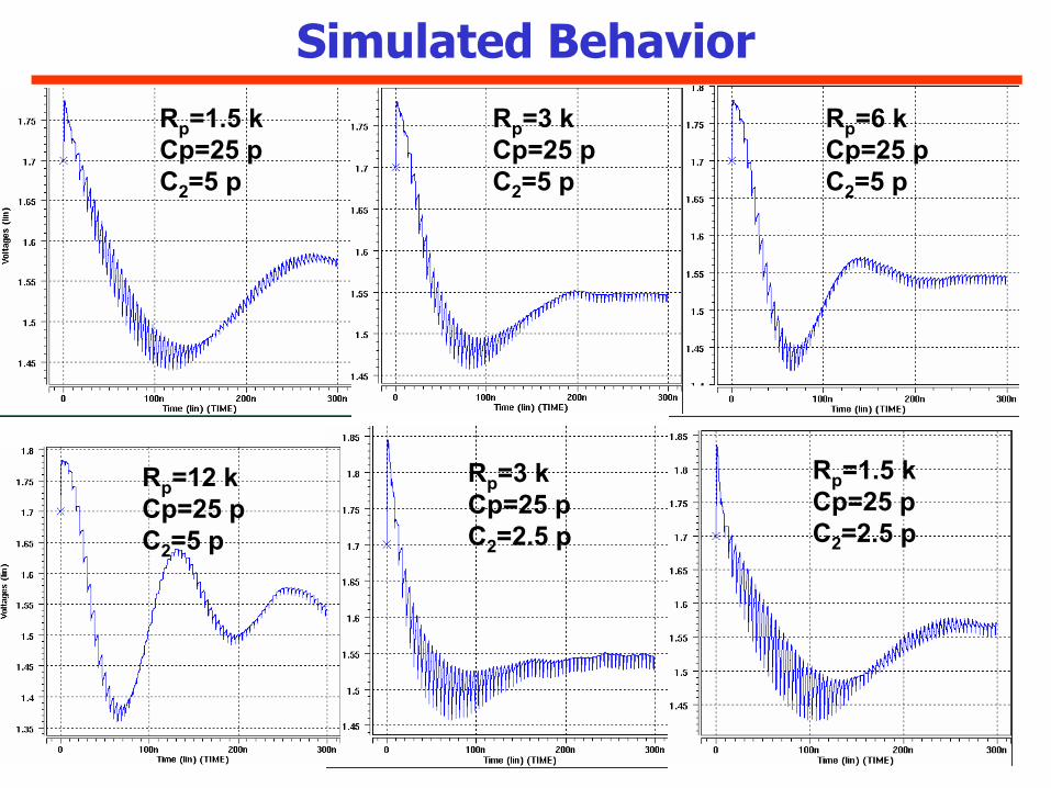
Simulated Behavior
Rp=3 kCp=25 pC2=2.5 p
Rp=1.5 kCp=25 pC2=2.5 p
Rp=1.5 kCp=25 pC2=5 p
Rp=3 kCp=25 pC2=5 p
Rp=6 kCp=25 pC2=5 p
Rp=12 kCp=25 pC2=5 p