Introduction to HDLmitmysore.in/downloads/ece/VERILOGmanualupdated.pdf · Introduction to HDL VHDL...
99
VERILOG 15ECL58 Dept of ECE,MIT MYSORE Page 1 Introduction to HDL VHDL stands for VHSIC (Very High Speed Integrated Circuit) Hardware Description Language. VHDL is a programming language that has been designed and optimized for describing the behavior of digital systems. VHDL has many features appropriate for describing the behavior of electronic components ranging from simple logic gates to complete microprocessors and custom chips. VHDL is also a general- purpose programming language: just as high-level programming languages allow complex design concepts to be expressed as computer programs, VHDL allows the behavior of complex electronic circuits to be captured into a design system for automatic circuit synthesis or for system simulation. One of the most important applications of VHDL is to capture the performance specification for a circuit, in the form of what is commonly referred to as a test bench. Test benches are VHDL descriptions of circuit stimuli and corresponding expected outputs that verify the behavior of a circuit over time. VHDL can describe a digital system at several different levels- Behavioral, Data-flow and Structural. A. Behavioral description: A digital circuit can be described at the behavioral level in terms of its function or behavior, without giving any implementation details. B. Data-flow description: A digital circuit can be described at the data-flow level by giving the logic equation of that circuit. C. Structural description: A digital circuit can be described at the structural level by specifying the interconnection of the gates or flip-flops that comprise the circuit.
Transcript of Introduction to HDLmitmysore.in/downloads/ece/VERILOGmanualupdated.pdf · Introduction to HDL VHDL...

VERILOG 15ECL58
Dept of ECE,MIT MYSORE Page 1
Introduction to HDL
VHDL stands for VHSIC (Very High Speed Integrated Circuit) Hardware Description
Language. VHDL is a programming language that has been designed and optimized for describing the
behavior of digital systems.
VHDL has many features appropriate for describing the behavior of electronic components
ranging from simple logic gates to complete microprocessors and custom chips. VHDL is also a general-
purpose programming language: just as high-level programming languages allow complex design
concepts to be expressed as computer programs, VHDL allows the behavior of complex electronic
circuits to be captured into a design system for automatic circuit synthesis or for system simulation.
One of the most important applications of VHDL is to capture the performance specification for
a circuit, in the form of what is commonly referred to as a test bench. Test benches are VHDL
descriptions of circuit stimuli and corresponding expected outputs that verify the behavior of a circuit
over time.
VHDL can describe a digital system at several different levels- Behavioral, Data-flow and Structural.
A. Behavioral description: A digital circuit can be described at the behavioral level in terms of its
function or behavior, without giving any implementation details.
B. Data-flow description: A digital circuit can be described at the data-flow level by giving the
logic equation of that circuit.
C. Structural description: A digital circuit can be described at the structural level by specifying
the interconnection of the gates or flip-flops that comprise the circuit.

VERILOG 15ECL58
Dept of ECE,MIT MYSORE Page 2
Verilog-HDL Lab manual
The basic design units used in VHDL are Entity and Architecture.
Entity: Entity is the basic design unit used in VHDL. It describes the external boundary of the
hardware.
General syntax of the entity is
entity entity-name is
port (list of ports: mode type;
list of ports: mode type);
end [ entity ][entity-name];
List of ports: which includes all input and output ports
Mode type: This specifies the type of ports such as in, out & inout.
Architecture: It describes the functionality/behaviour of the entity. General syntax of the architecture
is architecture architecture-name of entity-name is
[ declarations ]
begin
architecture body
end [architecture-name];
Note: 1. [ ] - square brackets indicates optional.
2. Signals and components are declared in the declaration part of the architecture.
3. The architecture body contains concurrent or sequential statements.
Process():
A common way of modelling sequential logic in VHDL uses a process. General syntax of the
process is
process (sensitivity-list)
begin

VERILOG 15ECL58
Dept of ECE,MIT MYSORE Page 3
Sequential-statements;
end process;
Sensitivity list contains list of signals. Whenever one of the signals in the sensitivity list changes the
sequential statements in the process body are executed in sequence one time.
If statement:
It is commonly used sequential statement. The basic IF statement has the
form if (condition) then
Sequential statements1
else
sequential statements2
end if;
The condition is a Boolean expression, which evaluates to TRUE or FALSE. If it is TRUE sequential
statements1 are executed otherwise sequential statements2 are executed.
Elsif statement: Which is alternative way of writing nested IF statements. The most general form of the
ELSIF statement is
if (condition) then
sequential statements
{ elsif (condition) then
sequential statements }
-- 0 or more elsif clauses may be
included. [else sequential statements ]
end if;
The curly brackets indicate that any number of elsif clauses may be included, and the square brackets
indicate that the else clause is optional.

VERILOG 15ECL58
Dept of ECE,MIT MYSORE Page 4
Conditional assignment statement:
This statement has the form
signal-name <= expression1 when condition1
else expression2 when condition2
…
[else expressionN ];
This concurrent statement is executed whenever an event occurs on a signal used in one of the
expressions or conditions.If condition1 is true, signal_name is set equal to the value of the expression1,
else if condition2 is true, signal_name is set equal to the value of expression2, etc.,
Case statement:
The case statement has the general form
case expression is
when choice1 => sequential statements1
when choice2 => sequential statements2
…
[ when others => sequential statements ]
end case;
The expression is evaluated first. If it is equal to “choice1”, then “sequential statements1” are
executed. If it is equal to “choice2”, then “sequential statements2” are executed, etc.,
Note: All the possible values of the expression must be included in the choices. If all the values are not
explicitly given, a “when others” clause is required in the case statement.
Variable:
Variable is a VHDL object and must be declared with in the process in which they are used and
are local to that process. The variable declaration has the form
variable list_of_variable_names : type_name [ := initial value ];

VERILOG 15ECL58
Dept of ECE,MIT MYSORE Page 5
Signal:
Signal is a VHDL object and it is declared in the declaration part of the
architecture. The signal declaration has the form
signal list_of_signal_names : type_name [ := initial value ];
Array:
The array type and array object declarations have the general forms
type array_type_name is array index_range of element_type;
Signal array_name: array_type_name [ := initial_values ];
element type: This specifies integer or bit or bit_vector etc.
VERILOG 15ECL58
Dept of ECE,MIT MYSORE Page 6
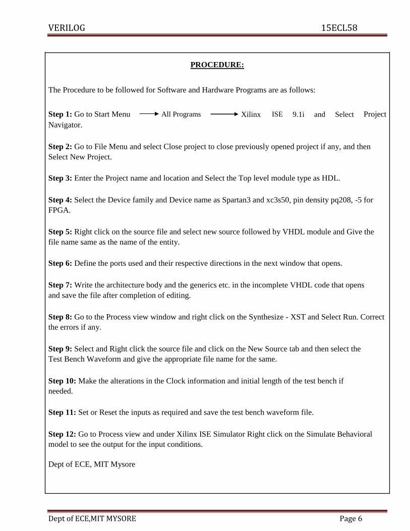
PROCEDURE:
The Procedure to be followed for Software and Hardware Programs are as follows:
Step 1: Go to Start Menu
All Programs
Xilinx
ISE
9.1i
and
Select
Project Navigator.
Step 2: Go to File Menu and select Close project to close previously opened project if any, and then
Select New Project.
Step 3: Enter the Project name and location and Select the Top level module type as HDL.
Step 4: Select the Device family and Device name as Spartan3 and xc3s50, pin density pq208, -5 for
FPGA.
Step 5: Right click on the source file and select new source followed by VHDL module and Give the
file name same as the name of the entity.
Step 6: Define the ports used and their respective directions in the next window that opens.
Step 7: Write the architecture body and the generics etc. in the incomplete VHDL code that opens
and save the file after completion of editing.
Step 8: Go to the Process view window and right click on the Synthesize - XST and Select Run. Correct
the errors if any.
Step 9: Select and Right click the source file and click on the New Source tab and then select the
Test Bench Waveform and give the appropriate file name for the same.
Step 10: Make the alterations in the Clock information and initial length of the test bench if
needed.
Step 11: Set or Reset the inputs as required and save the test bench waveform file.
Step 12: Go to Process view and under Xilinx ISE Simulator Right click on the Simulate Behavioral
model to see the output for the input conditions.
Dept of ECE, MIT Mysore

VERILOG 15ECL58
Dept of ECE,MIT MYSORE Page 7
Step 13: Make the appropriate connections between the PC and the FPGA kit for the observation of
outputs in the FPGA kit and for other Hardware Programming.
Step 14: Select and Right click the source file and click on the New Source tab and then select the
Implementation Constraints file and give the appropriate file name for the same. Step 15: Go to Process view and under User Constraints, double click on the Edit Constraints
(Text).
Step 16: Write the code for the user constraints file as required and save the same.
Step 17: Select the main source file and right click on the Implement design in the process view
window and select run.
Step 18: Right click on the Generate Programming file in the process view window and select run.
Step 19: Under the Generate Programming file tab, right click on the Configure device (Impact) and
click on the Run option.
Step 20: Select the appropriate mode and make changes in the jumper settings of the FPGA Kit as
required, select the appropriate.BIT extension file in the pop up window.
Step 21: Right click on the Chip picture in the pop up window and Select “Program”. Debug the errors
if it is there. Set the conditions for the inputs using Dip switch and observe the outputs.
**************

VERILOG 15ECL58
Dept of ECE,MIT MYSORE Page 8
Experiment No. 1
1. To write Verilog code to realize all the logic gates
A logic gate is an elementary building block of a digital circuit. It is an electronic device that
makes logical decisions based on the different combinations of digital signals present on its inputs A
digital logic gate may have more than one input but only has one digital output. At any given moment,
every terminal is in one of the two binary conditions low (0) or high (1), represented by different voltage
levels. There are seven basic logic gates: AND, OR, XOR, NOT, NAND, NOR, and XNOR.
i) NOT GATE: A logic gate whose input is complement of its input
Truth table Logic symbol
VERILOG CODE:
module not1(a,y);
input a;
output y;
assign y = ~a;
endmodule
OUTPUT:

VERILOG 15ECL58
Dept of ECE,MIT MYSORE Page 9
ii) AND GATE: A Logic circuit whose output is logic ‘1’ if and only if all of its inputs are logic ‘1’.
Truth table Logic symbol
VERILOG CODE:
module and1(a,b,y);
input a,b;
output y;
assign y = a & b;
endmodule
OUTPUT

VERILOG 15ECL58
Dept of ECE,MIT MYSORE Page 10
iii) OR GATE: A logic gate whose output is logic ‘0’ if and only if all of its inputs are logic ‘0’.
Truth table Logic symbol
VERILOG CODE:
module or1(a,b,y);
input a,b;
output y;
assign y = a | b;
endmodule
OUTPUT:

VERILOG 15ECL58
Dept of ECE,MIT MYSORE Page 11
iv) NAND GATE: A logic gate which gives logic ‘0’ output if and only if all of its inputs are logic
‘1’.
Truth table Logic symbol
VERILOG CODE:
module nand1(a,b,y);
input a,b;
output y;
assign y = ~(a & b);
endmodule
OUTPUT:

VERILOG 15ECL58
Dept of ECE,MIT MYSORE Page 12
v) NOR GATE: A logic gate whose output logic ‘1’ if and only if all of its inputs are logic ‘0’
Truth table Logic symbol
VERILOG CODE:
module nor1(a,b,y);
input a,b;
output y;
assign y = ~(a | b);
endmodule
OUTPUT:

VERILOG 15ECL58
Dept of ECE,MIT MYSORE Page 13
vi) EX-OR (Exclusive OR): A logic gate whose output is logic ‘0’ when all the inputs are equal and
logic ‘1’ when they are unequal.
Truth table Logic Symbol
VERILOG CODE:
module xor1(a,b,y);
input a,b;
output y;
assign y = a ^ b;
endmodule
OUTPUT:

VERILOG 15ECL58
Dept of ECE,MIT MYSORE Page 14
vii) EX-NOR (Exclusive -NOR) gate: A logic gate that prodices a logic ‘1’ only when the two inputs
are equal
Truth table
symbol
VERILOG CODE:
module xnor1(a,b,y);
input a,b;
output y;
assign y = ~(a ^ b);
endmodule
OUTPUT:

VERILOG 15ECL58
Dept of ECE,MIT MYSORE Page 15
ALL LOGIC GATES TOGETHER:
VERILOG CODE:
module gates(a,b,op_not,op_or,op_nor,op_xor,op_xnor,op_and,op_nand);
input a,b;
output op_not,op_or,op_nor,op_xor,op_xnor,op_and,op_nand;
assign op_not =~a;
assign op_or = a | b;
assign op_nor = ~(a | b);
assign op_xor = a ^ b;
assign op_xnor = ~(a ^ b);
assign op_and = a & b;
assign op_nand = ~(a & b);
endmodule
OUTPUT:
RESULT: The logic gates designs have been realized and simulated using HDL codes.

VERILOG 15ECL58
Dept of ECE,MIT MYSORE Page 16
APPLICATIONS:
In practice, the gates are made from field-effect transistors (FETs), particularly MOSFETs (metal–oxide–semiconductor field-effect transistors).
Logic circuits include devices such as multiplexers, registers, arithmetic logic units (ALUs), and
computer memory, all the way up through complete microprocessors, which may contain more
than 100 million gates.
Compound logic gates AND-OR-Invert (AOI) and OR-AND-Invert (OAI) are often employed in
circuit design because their construction using MOSFETs is simpler and more efficient than the
sum of the individual gates.
Every digital product, like computers, mobile, calculators even digital watches, contain logic gates.
Probable Viva Questions:
1. Give expansion for the following, VHDL, FPGA, CPLD, ASIC’s, ISP, IEEE, PLD, and JTAG. 2. Which are the two IEEE standard HDL languages? 3. Which IEEE standard used to write HDL? 4. What is synthesis? Which synthesis tool is used in the lab? 5. What is simulator? Which simulator tool is used in the lab? 6. Define signal, variable, constant. 7. What are the different types of assignment statements? 8. What do you mean by keywords? List some of the key words of VHDL and Verilog.

VERILOG 15ECL58
Dept of ECE,MIT MYSORE Page 17
EXPERIMENT NO. 2
2. Write a Verilog code for the following combinational designs.
2.a) 2 to 4 decoder: A decoder is a digital logic circuit that converts n-bits binary input code in to M
output lines. OR It is a logic circuit that decodes from binary to octal, decimal, Hexa-decimal or any
other code such as 7-segment etc.
Block Diagram:
Truth table:
E Sel1 Sel0 Y3 Y2 Y1 Y0
0 0 0 0 0 0 1
0 0 1 0 0 1 0
0 1 0 0 1 0 0
0 1 1 1 0 0 0
1 X X 0 0 0 0

VERILOG 15ECL58
Dept of ECE,MIT MYSORE Page 18
Logic diagram:
1) Data flow description:
VERILOG CODE:
module dec2 (a,b,e,y1,y2,y3,y4);
input a, b, e;
output y1, y2, y3, y4;
wire s0, s1, s2;
assign s0 = ~a;
assign s1 = ~b;
assign s2 = ~e;
assign y1 = s0 & s1 & s2;
assign y2 = s0 & b & s2;
assign y3 = a & s1 & s2;
assign y4 = a & b & s2;
endmodule.

VERILOG 15ECL58
Dept of ECE,MIT MYSORE Page 19
2)
Behavi
oral description:
VERILOG CODE:
module dec24 (i, e, y);
input [1:0] I;
input e;
output [3:0] y;
reg [3:0] y;
always @(i, e)
begin
if (e== 0)
begin
case(i)
2’b 00: y = 4’b 0001;
2’b 01: y = 4’b 0010;
2’b 10: y = 4’b 0100;
2’b 11: y = 4’b 1000;
endcase
end
else
y = 4’b 0000;
end
endmodule.

VERILOG 15ECL58
Dept of ECE,MIT MYSORE Page 20
2 to 4 DECODER (using if else statement)
VERILOG CODE:
module decoder2_4 (e,i,y);
output[3:0]y;
input[1:0]i;
input e ;
reg [3:0]y;
always@(i or e)
begin
if(e==0)
if(i==0) y=4'b 0001;else
if(i==1) y=4'b 0010;else
if(i==2) y=4'b 0100;else
if(i==3) y=4'b 1000;else
y=4' bx;
end
endmodule
3)Structural Description :
VERILOG CODE:
module dec24 (e,a,b,y1,y2,y3,y4);
input e, a, b;
output y1, y2, y3, y4;
wire s0,s1,s2;
not n1(s0,a);
not n2 (s1,b);
not n3 (s2,e);
and a1(y1,s0,s1,s2);
and a2(y2,s0,b,s2);
and a3(y3,a,s1,s2);
and a4(y4,a,b,s2);
endmodule

VERILOG 15ECL58
Dept of ECE,MIT MYSORE Page 21
OUTPUT:
RESULT: The 2 to 4 decoder design have been realized and simulated using HDL codes.
APPLICATIONS:
Decoding is necessary in applications such as data multiplexing, 7 segment display and memory address
decoding, wireless control systems.

VERILOG 15ECL58
Dept of ECE,MIT MYSORE Page 22
2.b. To write a Verilog Code to realize an 8 to 3 Encoder without priority and with
priority.
Encoder: The term ‘encode’ specifies the conversion of information(number or character) into a coded
form. An encoder is a combinational logic circuit that converts information such as a decimal number or
an alphabetic character, into some coded form. An encoder accepts an active level on one of its inputs
representing a digit, such as decimal or octal digit, and converts it to a coded output, such as binary or
BCD.
Priority encoder: Whenever two or more inputs are applied at a time, internal hardware will check this
condition and if the priority is set such that higher numbered input should be taken into account and
remaining are considered as don’t care then output code will be appear will be “higher numbered input”.
Block Diagram:
Truth table:
I/P (I) O/P (Y)
00000001 000
00000010 001
00000100 010
00001000 011
00010000 100
00100000 101
01000000 110
10000000 111

VERILOG 15ECL58
Dept of ECE,MIT MYSORE Page 23
Logic diagram:
VERILOG CODE:
module enc83(i, y);
input [7:0]i;
output [2:0]y;
reg [2:0]y;
always@ (i)
begin
case (i)
8'b 00000001: y = 3'b 000;
8'b 00000010: y = 3'b 001;
8'b 00000100: y = 3'b 010;
8'b 00001000: y = 3'b 011;
8'b 00010000: y = 3'b 100;
8'b 00100000: y = 3'b 101;
8'b 01000000: y = 3'b 110;
8'b 10000000: y = 3'b 111;
default: y = 3'b zzz;
endcase
end
endmodule

VERILOG 15ECL58
Dept of ECE,MIT MYSORE Page 24
/* alternative description is given below
Module encoder (code, data);
Output [2:0] code;
Input [7:0] data;
Reg [2:0] code;
always @ (data)
begin
if (data=8’b 00000001) code=0;else
if (data=8’b 00000010) code=1;else
if (data=8’b 00000100) code=2;else
if (data=8’b 00001000) code=3;else
if (data=8’b 00010000) code=4;else
if (data=8’b 00100000) code=5;else
if (data=8’b 01000000) code=6;else
if (data=8’b 10000000) code=7;else
code=3’bx;
end
endmodule
OUTPUT:
RESULT : The 8 to 3 encoder design have been realized and simulated using verilog code

VERILOG 15ECL58
Dept of ECE,MIT MYSORE Page 25
8 to 3 ENCODER with priority:
Truth table
I/P (I) O/P (Y)
1XXXXXXX 111
01XXXXXX 110
001XXXXX 101
0001XXXX 100
00001XXX 011
000001XX 010
0000001X 001
00000001 000
VERILOG CODE:
module priority (code, data);
output [2:0] code;
input [7:0]data;
reg [2:0]code;
always @ (data)
begin
if(data[7]) code=7;else
if(data[6]) code=6;else
if(data[5]) code=5;else
if(data[4]) code=4;else
if(data[3]) code=3;else
if(data[2]) code=2;else if(data[1]) code=1;else
if(data[0]) code=0;else
code= 3’bx;
end endmodule

VERILOG 15ECL58
Dept of ECE,MIT MYSORE Page 26
OUTPUT:
RESULT : The 8 to 3 encoder design have been realized and simulated using HDL codes.
APPLICATIONS :
Encoding is used in most wireless control systems to prevent interference. It is useful in web processes,
handling and inspection systems that use conveyors and simple speed or position control in high
vibration environments.
VERILOG 15ECL58
Dept of ECE,MIT MYSORE Page 27
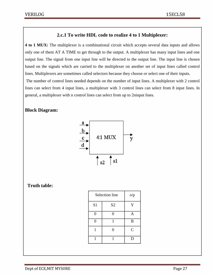
2.c.1 To write HDL code to realize 4 to 1 Multiplexer:
4 to 1 MUX: The multiplexer is a combinational circuit which accepts several data inputs and allows
only one of them AT A TIME to get through to the output. A multiplexer has many input lines and one
output line. The signal from one input line will be directed to the output line. The input line is chosen
based on the signals which are carried to the multiplexer on another set of input lines called control
lines. Multiplexers are sometimes called selectors because they choose or select one of their inputs. The number of control lines needed depends on the number of input lines. A multiplexer with 2 control
lines can select from 4 input lines, a multiplexer with 3 control lines can select from 8 input lines. In
general, a multiplexer with n control lines can select from up to 2ninput lines.
Block Diagram:
Truth table:
Selection line o/p
S1 S2 Y
0 0 A
0 1 B
1 0 C
1 1 D

VERILOG 15ECL58
Dept of ECE,MIT MYSORE Page 28
Circuit diagram:
1) Data flow: VERILOG CODE:
module mux41(a,b,c,d,s1,s2, y);
input a,b,c,d,s1,s2;
output y;
wire m1,m2,m3,m4,m5,m6;
assign m1 = ~s1;
assign m2 = ~s2;
assign m3 = m1 & m2 & a;
assign m4 = m1 & s2 & b;
assign m5 = s1 & m2 & c;
assign m6 = s1 & s2 & d;
assign y = m3 | m4 | m5 | m6;
endmodule

VERILOG 15ECL58
Dept of ECE,MIT MYSORE Page 29
Behavioral:
VERILOG CODE:
module mux41(i,s,y);
input [3:0] i;
input [1:0] s;
output y;
reg y;
always@(i,s)
begin
case(s)
2'b 00: y = i[0];
2'b 01: y = i[1];
2'b 10: y = i[2];
2'b 11: y = i[3];
endcase
end
endmodule
Structural:
VERILOG CODE:
module mux41 (a,b,c,d,s1,s2,y);
input a, b, c, d, s1, s2;
output y;
wire m1,m2,m3,m4,m5,m6;
not n1(m1,s1);
not n2 (m2,s2);
and a1(m3,m1,m2,a);
and a2(m4,s1,m2,b);
and a3(m5,m1,s2,c);
and a4(m6,s1,s2,d);
or o1(y,m3,m4,m5,m6);
endmodule

VERILOG 15ECL58
Dept of ECE,MIT MYSORE Page 30
OUTPUT:
RESULT : The 4 to 1 multiplexer design have been realized and simulated using HDL codes.
APPLICATIONS: Multiplexers are used in building digital semiconductors such as central processing
units (CPUs) and graphics controllers. They are also used in communications.cross bar switch, cellphone
systems, instrumentation, and any other function where only one transmission channel (e.g a radio
transmitter) is available. They mostly find in numerous and varied applications in digital systems of all
types such as data selection, data routing, operation sequencing, parallel-to-serial conversion, waveform
generation and logic-function generation.

VERILOG 15ECL58
Dept of ECE,MIT MYSORE Page 31
2.c.2 To write a Verilog Code to realize an 8 to 1 Multiplexer.
Multiplexer is simply a data selector. It has multiple inputs and one output. Any one of the input line is
transferred to output depending on the control signal. This type of operation is usually referred as
multiplexing .In 8:1 multiplexer ,there are 8 inputs. Any of these inputs are transferring to output ,which
depends on the control signal. For 8 inputs we need ,3 bit wide control signal . If control signal is "000"
,then the first input is transferring to output line. If control signal is "111",then the last input is
transferring to output. Similarly for all values of control signals.
Block diagram:
Truth table:
Selection line Output
S2 S1 S0 Y
0 0 0 i(0)
0 0 1 i(1)
0 1 0 i(2)
0 1 1 i(3)
1 0 0 i(4)
1 0 1 i(5)
1 1 0 i(6)
1 1 1 i(7)

VERILOG 15ECL58
Dept of ECE,MIT MYSORE Page 32
Logic Diagram:
VERILOG Code:
module mux81(i,s,y);
input [7:0] i;
input [2:0] s;
output y;
reg y;
always@(i or s)
begin
case(s) 3'b 000: y = i[0];
3'b 001: y = i[1];
3'b 010: y = i[2];
3'b 011: y = i[3];
3'b 100: y = i[4];
3'b 101: y = i[5];
3'b 110: y = i[6];
3'b 111: y = i[7];
endcase
end
endmodule

VERILOG 15ECL58
Dept of ECE,MIT MYSORE Page 33
OUTPUT:
RESULT : The 8 to 1 multiplexer design have been realized and simulated using HDL codes.

VERILOG 15ECL58
Dept of ECE,MIT MYSORE Page 34
2.d. 1:4 Demultiplexer
The demultiplexer takes one single input data line and then switches it to any one of the number of
individual output lines one at a time. The demultiplexer converts a serial data signal at the input to a
parallel data at its output lines. The function of the 1 : 4 Demultiplexer is to switch one common data
input line to any one of the 4 output data lines.
Block Diagram:
Truth Table:
S(1) S(0) i Y0 Y1 Y2 Y3
0 0 0 0 0 0 0
0 0 1 1 0 0 0
0 1 0 0 0 0 0
0 1 1 0 1 0 0
1 0 0 0 0 0 0
1 0 1 0 0 1 0
1 1 0 0 0 0 0
1 1 1 0 0 0 1

VERILOG 15ECL58
Dept of ECE,MIT MYSORE Page 35
Logic diagram:
VERILOG CODE:
module demux1to4( din,sel,out);
output [3:0] out;
input [1:0] sel;
input din;
reg [3:0] out;
always @ (sel,din)
begin
out=4'b0000;
case(sel)
2'b 00 : out[0]=din;
2'b 01 : out[1]=din;
2'b 10 : out[2]=din;
2'b 11 : out[3]=din;
endcase
end
endmodule

VERILOG 15ECL58
Dept of ECE,MIT MYSORE Page 36
OUTPUT:
RESULT: The 1 to 4 demultiplexer design have been realized and simulated using HDL codes.
APPLICATIONS: Demultiplexers are used in Clock demultiplexer, Security monitoring
system, Synchronous data transmission system
VERILOG 15ECL58
Dept of ECE,MIT MYSORE Page 37
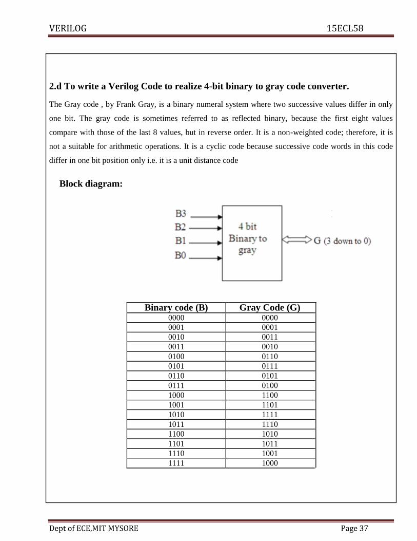
2.d To write a Verilog Code to realize 4-bit binary to gray code converter.
The Gray code , by Frank Gray, is a binary numeral system where two successive values differ in only
one bit. The gray code is sometimes referred to as reflected binary, because the first eight values
compare with those of the last 8 values, but in reverse order. It is a non-weighted code; therefore, it is
not a suitable for arithmetic operations. It is a cyclic code because successive code words in this code
differ in one bit position only i.e. it is a unit distance code
Block diagram:
Binary code (B) Gray Code (G) 0000 0000
0001 0001
0010 0011
0011 0010
0100 0110
0101 0111
0110 0101
0111 0100
1000 1100
1001 1101
1010 1111
1011 1110
1100 1010
1101 1011
1110 1001
1111 1000

VERILOG 15ECL58
Dept of ECE,MIT MYSORE Page 38
Logic Diagram:
1) Data flow description VERILOG CODE:
Module bin_gray(b,g);
input [3:0]b;
output [3:0] g;
assign g[3]=b[3];
assign g[2] = b[2] ^ b[3];
assign g[1] = b[2] ^ b[1];
assign g[0] = b[1] ^ b[0];
endmodule

VERILOG 15ECL58
Dept of ECE,MIT MYSORE Page 39
2) Structural Description: VERILOG CODE:
Module bin_gray(b,g);
input [3:0]b;
output [3:0] g;
assign g[3]=b[3];
xor (g[2],b[3],b[2]);
xor (g[1],b[2],b[1]);
xor (g[0],b[1],b[0]);
endmodule
OUTPUT:
RESULT: The 4 bit binary to gray converter design have been realized and simulated using HDL codes.
APPLICATIONS: Gray codes are widely used to facilitate error correction in digital communications
such as digital terrestrial television and some cable TV systems.

VERILOG 15ECL58
Dept of ECE,MIT MYSORE Page 40
2.f. Comparator: A circuit that compares two numbers and produces an output indicating whether
they are equal. It may also indicate which number is greater if they are unequal. Ex: ‘1’ bit comparator
Block Diagram:
Truth Table:
A B A>B A=B A<B
0 0 0 1 0
0 1 0 0 1
1 0 1 0 0
1 1 0 1 0
Circuit Diagram:

VERILOG 15ECL58
Dept of ECE,MIT MYSORE Page 41
VERILOG CODE:
module comp(a,b,g,l,e);
input a,b;
output g,l,e;
xnor (e,a,b);
and (g,a,~b);
and (l,~a,b);
endmodule
OUTPUT:
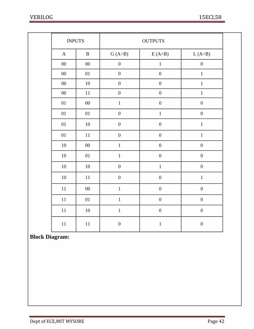
2-BIT COMPARATOR :
A digital comparator is a hardware electronic device that compares two numbers in binary form
and generates a one or a zero at its output depending on whether they are the same or not. A 2 bit
comparator compares two 2-bit binary, BCD, or other monotonic codes and presents the three possible
magnitude results at the outputs i.e., a>b, a<b, a=b.
Block Diagram:
A 2-BIT A>B
COMPAR
ATOR A=B
B A<B
Truth Table:
VERILOG 15ECL58
Dept of ECE,MIT MYSORE Page 42
INPUTS OUTPUTS
A B G (A>B) E (A=B) L (A<B)
00 00 0 1 0
00 01 0 0 1
00 10 0 0 1
00 11 0 0 1
01 00 1 0 0
01 01 0 1 0
01 10 0 0 1
01 11 0 0 1
10 00 1 0 0
10 01 1 0 0
10 10 0 1 0
10 11 0 0 1
11 00 1 0 0
11 01 1 0 0
11 10 1 0 0
11 11 0 1 0
Block Diagram:

VERILOG 15ECL58
Dept of ECE,MIT MYSORE Page 43
VERILOG CODE:
module COMP4(a,b, les, grt, equ);
input [1:0] a,b;
output les, grt, equ;
reg les, grt, equ;
always @(a,b)
begin
les =0;
grt =0;
equ =0;
if (a<b)
les =1;
else if (a == b)
equ =1;
else
grt =1;
end
endmodule

VERILOG 15ECL58
Dept of ECE,MIT MYSORE Page 44
OUTPUT:
RESULT: The 4 bit comparator design have been realized and simulated using HDL codes.
APPLICATIONS: In mass production, where components are to be checked at a very fast rate.
In selective assembly of parts, where parts are graded in three or more groups depending upon their tolerance.
Probable viva Questions:
1. Define Comparator.
2. What is the application of comparator?
3. Why we need to use comparator?
4. What is the difference between analog comparator to digital comparator?
5. In which field comparator plays an important role?
6. What is key difference between sequential and combinational circuits?
7. What are applications of multiplexers?
8. Write short note on transport delay.
9. Write about behavioral models.
10. Write short note on delta delay.
11. What are hardware description languages?

VERILOG 15ECL58
Dept of ECE,MIT MYSORE Page 45
12. Write short note on inertial delay.
13. Mention the applications of comparators, encoders, Mux, Demux, decoders.
14. How do we choose the appropriate type of description for the given program?
15. Why we need covertion techniques?
16. Application of gray to binary and binary to gray conversion.
17. Define MUX with example.
18. Define DeMUX with example.
19. Why we need to convert from binary to gray code and vice versa.

VERILOG 15ECL58
Dept of ECE,MIT MYSORE Page 46
Experiment No. 3
Write a VHDL and Verilog code to describe the functions of a FULL ADDER using Following
modeling styles.
Block Diagram:
Truth Table:
Ain Bin Cin Sum Cout
0 0 0 0 0
0 0 1 1 0
0 1 0 1 0
0 1 1 0 1
1 0 0 1 0
1 0 1 0 1
1 1 0 0 1
1 1 1 1 1
Logic Diagram:

VERILOG 15ECL58
Dept of ECE,MIT MYSORE Page 47
1) DATAFLOW Description:
VHDL Code
library IEEE;
use IEEE.STD_LOGIC_1164.ALL;
entity full_adder is
Port ( a,b,cin: in std_logic;
sum,cout: out std_logic);
end full_adder;
architecture dataflow of full_adder is
begin
sum<=a xor b xor cin;
cout<=(a and b) or (b and cin) or (cin and a);
end dataflow;
VERILOG CODE:
module fad(a,b,cin, sum,cout);
input a,b,cin;
output sum,cout;
assign sum = a ^ b ^ cin;
assign cout = (a & b) | (b & cin) | (a &
cin); endmodule

VERILOG 15ECL58
Dept of ECE,MIT MYSORE Page 48
BEHAVIORAL VHDL CODE
library ieee ;
use ieee.std_logic_1164.all;
entity fad is
port(a,b,cin: in std_logic;
sum, cout : out std_logic);
end fad;
architecture beh of fad is
begin
process(a,b,cin)
begin
if (a = ‘0’ and b =’0’ and cin = ‘0’) then
sum <= ‘0’; cout <= ‘0’;
elsif (a = ‘0’ and b =’0’ and cin = ‘1’) then
sum <= ‘1’; cout <= ‘0’;
elsif (a = ‘0’ and b =’1’ and cin = ‘0’) then
sum <= ‘1’; cout <= ‘0’;
elsif (a = ‘0’ and b =’1’ and cin = ‘1’) then
sum <= ‘0’; cout <= ‘1’;
elsif (a = ‘1’ and b =’0’ and cin = ‘0’) then
sum <= ‘1’; cout <= ‘0’;
elsif (a = ‘1’ and b =’0’ and cin = ‘1’) then
sum <= ‘0’; cout <= ‘1’;
elsif (a = ‘1’ and b =’1’ and cin = ‘0’) then
sum <= ‘0’; cout <= ‘1’;
elsif (a = ‘1’ and b =’1’ and cin = ‘1’) then
sum <= ‘1’; cout <= ‘1’;
endif;
end process;
end beh;

VERILOG 15ECL58
Dept of ECE,MIT MYSORE Page 49
VERILOG CODE:
module nm(a,b,cin, sum, cout);
input a,b,cin;
output sum, cout;
reg sum, cout;
always @ (a,b, cin)
begin
if(a==0 & b==0 & cin==0)
begin
sum = 0; cout =0;
end
else if(a==0 & b==0 & cin==1)
begin
sum = 1; cout =0;
end
else if(a==0 & b==1 & cin==0)
begin
sum = 1; cout =0;
end
else if(a==0 & b==1 & cin==1)
begin
sum = 0; cout =1;
end
else if(a==1 & b==0 & cin==0)
begin
sum = 1; cout =0;
end
else if(a==1 & b==0 & cin==1)
begin
sum = 0; cout =1;

VERILOG 15ECL58
Dept of ECE,MIT MYSORE Page 50
end
else if(a==1 & b==1 & cin==0)
begin
sum = 0; cout =1;
end
else if(a==1 & b==1 & cin==1)
begin
sum = 1; cout =1;
end end endmodule
Logic Diagram:
STRUCTURAL Description:
VHDL CODE
library IEEE;
use IEEE.STD_LOGIC_1164.ALL;
entity FullAdder is
Port ( Ain, Bin, Cin : in std_logic;
Sum, Cout : out std_logic);
end FullAdder;
architecture structl of FullAdder is
Component Halfadder
Port ( a, b : in std_logic; Sum, Carry : out std_logic);
end Component;

VERILOG 15ECL58
Dept of ECE,MIT MYSORE Page 51
Component orgate
Port ( a, b : in std_logic; y : out std_logic);
end Component;
Signal temp1, temp2, temp3: std_logic; -- Signal Declaration
begin L1: Halfadder port map ( Ain, Bin,temp1,temp2);
L2: Halfadder port map ( temp1,Cin,Sum,temp3);
L3: orgate port map (temp2, temp3,Cout);
end struct;
Half Adder circuit
--Low level modules—
--component halfadder--
library IEEE;
use IEEE.STD_LOGIC_1164.ALL;
entity Halfadder is Port (a,b : in std_logic; Sum, Carry: out std_logic);
end Halfadder; architecture dataflow of Halfadder is
begin
Sum <= a xor b;
Carry<= a and b;
end dataflow;
---- component orgate----
library IEEE;
use IEEE.STD_LOGIC_1164.ALL;
entity orgate is
Port ( a, b : in std_logic; y : out std_logic);
end orgate;
architecture dataflow of orgate is
begin
y<= a or b;
end dataflow;

VERILOG 15ECL58
Dept of ECE,MIT MYSORE Page 52
VERILOG CODE:
module Fulladd (x,y,cin,sum,carry);
input x,y,cin;
output sum,carry;
HA H1(y,cin,s0,c0);
HA H2(x,s0,sum,c1);
or (carry,c0,c1);
endmodule
module HA (a,b,s,c);
input a,b;
output s,c;
xor(s,a,b);
and (c,a,b);
endmodule
OUTPUT:

VERILOG 15ECL58
Dept of ECE,MIT MYSORE Page 53
RESULT: Three modeling styles of full adder have been realized and simulated using HDL codes.
APPLICATIONS: Adders and Subtractors can be used in op amp circuits, that is as comparators or
differentiators. Arithmetic operations are extensively used in many VLSI applications such as signal
processing, and digital communication. Adders are basically used in calculators. They are used in all
processors – micrprocessors and microcontrollers and also DSP processors.
Probable Viva Questions:
1. What is the difference between the adders constructing using IC and basic gates?
2. What is the advantage of using IC’s to construct the adders and subtractor.
3. Define parallel adder and parallel subtractor.
4. What is the difference between parallel adder and parallel constructor?
5. What is the need of code conversion?
6. Define adders and subtractor.

VERILOG 15ECL58
Dept of ECE,MIT MYSORE Page 54
Experiment No. 4
3. To write a Verilog Code to realize a 4-bit ALU.
Opcode ALU Operation
0 A+B
1 A-B
2 A OR B
3 A AND B
4 NOT A
5 A*B
6 A NAND B
7 A XOR B
Block Diagram:
Truth Table:

VERILOG 15ECL58
Dept of ECE,MIT MYSORE Page 55
VERILOG CODE:
module alu4(a,b, opcode, y, e);
input [3:0] a,b;
input [2:0] opcode;
output [7:0] y;
input e;
reg [7:0] y;
always @ (a,b,e,opcode)
begin
y = 8'd0;
if(e==0)
y = 8'dZ;
else
case(opcode)
4'd0 : y = a + b;
4'd1 : y = a - b;
4'd2 : y = a | b ;
4'd3 : y = a & b;
4'd4 : y = ~a ;
4'd5 : y = a * b;
4'd6 : y = ~(a & b);
4'd7 : y = a ^ b;
endcase
end
endmodule
RESULT: 32 bit ALU operations have been realized and simulated using HDL codes.
APPLICATIONS : Arithmetic Logic Unit is used extensively for Signal Processing and Control. It can be used in many applications involving arithmetic
operations. Many DSP and control applications require a small subset of arithmetic operations that must be computed efficiently.
VERILOG 15ECL58
Dept of ECE,MIT MYSORE Page 56
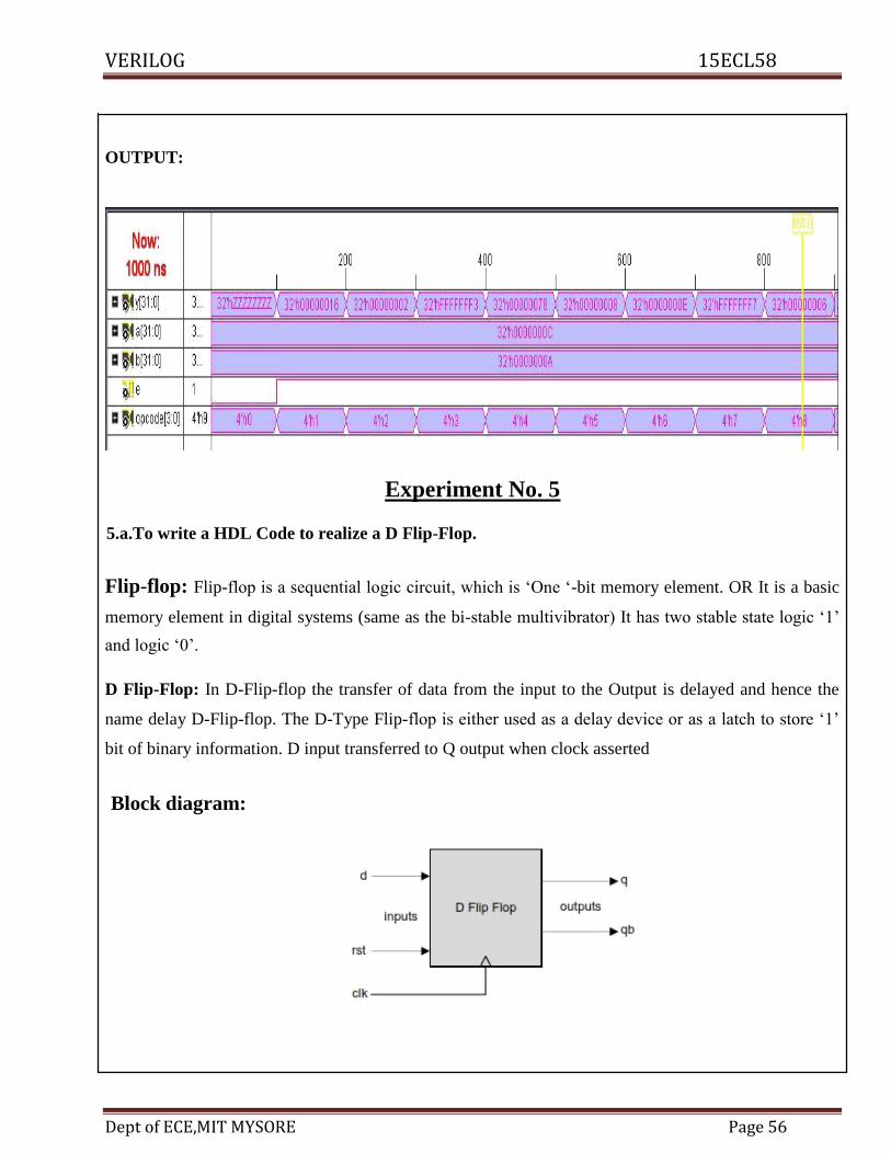
OUTPUT:
Experiment No. 5
5.a.To write a HDL Code to realize a D Flip-Flop.
Flip-flop: Flip-flop is a sequential logic circuit, which is ‘One ‘-bit memory element. OR It is a basic
memory element in digital systems (same as the bi-stable multivibrator) It has two stable state logic ‘1’
and logic ‘0’.
D Flip-Flop: In D-Flip-flop the transfer of data from the input to the Output is delayed and hence the
name delay D-Flip-flop. The D-Type Flip-flop is either used as a delay device or as a latch to store ‘1’
bit of binary information. D input transferred to Q output when clock asserted
Block diagram:

VERILOG 15ECL58
Dept of ECE,MIT MYSORE Page 57
Truth table:
Inputs Outputs
RST CLK D q qbar
1 ↑ x 0 1
0 ↑ 0 0 1
0 ↑ 1 1 0
VERILOG CODE:
module d_ff( d , clk , reset , q ,qb ); input d, clk, reset ;
output q,qb;
reg q,qb;
always @ ( posedge clk or posedge reset)
if (reset)
begin
q = 1'b0;
qb=~q;
end
else
begin
q = d;
qb=~q;
end
endmodule OUTPUT:

VERILOG 15ECL58
Dept of ECE,MIT MYSORE Page 58
5.b.To write a Verilog Code to realize a T Flip-Flop.
T Flip-Flop: On every change in clock pulse the output ‘Q’ changes its state (Toggle). A
Flip-flop with one data input which changes state for every clock pulse.(J=K=’1’ in JQK
Flip-flop the resulting output is ‘T’ Flip-flop)
Block diagram:
Truth table:
Inputs Outputs
RST CLK T q qb Action
1 ↑ x 0 1 Reset
0 ↑ 0 q qb No change
0 ↑ 1 q’ qb’ Toggle

VERILOG 15ECL58
Dept of ECE,MIT MYSORE Page 59
VERILOG CODE:
module t_ff( t, clk, reset, q, qb );
input t, clk, reset ;
output q,qb;
reg q,qb;
always @ ( posedge clk or posedge reset)
if (reset)
begin
q = 1'b0;
qb=~q;
end
else
if (t)
begin
q = ~q;
qb = ~q;
end
endmodule
OUTPUT :

VERILOG 15ECL58
Dept of ECE,MIT MYSORE Page 60
5.c. To write a HDL Code to realize a SR Flip-Flop:
SR Flip-Flop: In a memory device set and Reset is often required for synchronization of the device
in such case S-R Flip-flop is need & this is refereed as clocked set-reset.
Block diagram:
Truth table:
Inputs Outputs
RST CLK S R q qb Action
1 ↑ x x 0 1 Reset
0 ↑ 0 0 q qb No change
0 ↑ 0 1 0 1 Reset
0 ↑ 1 0 1 0 Set
0 ↑ 1 1 - - Illegal

VERILOG 15ECL58
Dept of ECE,MIT MYSORE Page 61
VERILOG CODE:
module srff(SR,clk, rst, Q,Qbar);
input[1:0] SR;
input clk, rst;
output Q,Qbar;
reg Q,Qbar;
always @(posedge clk)
begin
if (rst == 1)
Q = 0;
else
begin
casex(SR)
2'b00:Q=Q;
2'b01:Q=0;
2'b10:Q=1;
2'b11:Q=1'bX;
Endcase
end
Qbar=~Q;
end
endmodule
OUTPUT:

VERILOG 15ECL58
Dept of ECE,MIT MYSORE Page 62
5.d. To write a HDL Code to realize a JK Flip-Flop.
JK Flip-Flop: The race conditions in S-R Flip-flop can be eliminated by converting it in to J.K
Block diagram:
Truth Table: Preset(sn) Clear(rn) J K Clk q qb Action
0 1 X X X 1 0 Set
VERILOG
1 0 X X X 0 1 Reset
module jkff(JK,clk,
1 1 0 0 ↑ q qb No
input [1:0] JK; change
1 1 0 1 ↑ 0 1 Reset input clk;
1 1 1 0 ↑ 1 0 Set output Q,Qbar;
1 1 1 1 ↑ q’ qb’ Toggle reg Q,Qbar;
always @ (posedge clk)
begin
case(JK)
2'd0 : Q = Q;
2'd1 : Q = 0;
2'd2 : Q = 1;
2'd3 : Q = ~Q;
endcase
Qbar = ~Q;
end
endmodule

VERILOG 15ECL58
Dept of ECE,MIT MYSORE Page 63
OUTPUT:
Probable Viva Questions:
1. What are different types of ROM,s.
2. What are applications of flip flops.
3. Explain resolution functions.
4. How does look-a head carry adder speed up the addition process.
5. What is parity bit generator.
6. What are steps involved in implementation and anlysis of digital systems.
7. What are capabilities of VHDL.
8. Explain the significance of conditional signal assignment statement and selected
9. signal assignment statement.
10. How will you compare component declaration and component instantiation.
11. Write down the configuration specification for full adder circuit.
12. Write down the VHDL code of following:
(a)D-flip flop
(b) T-flip flop
13. Write down the VHDL code of S-R flip flop.
14. What are generics?
15. Explain with example that how a component can be made more general using
generics.
16. What are sequential statements? Write down its syntax.
17. Discuss process and wait statements.
18. How are sequential statements different from concurrent statements?
19. Write a short note on package and library.

VERILOG 15ECL58
Dept of ECE,MIT MYSORE Page 64
Experiment No. 6
COUNTER: Counter is a digital circuit that can counts the member of pulse for building the counters,
Flip-flop are used. Relation between number of Flip-flop used and number of state of counter is
(Regular/binary counter)
Synchronous Counter:
Ripple Counter/Asynchronous Counter:
6.1 Binary Synchronous Reset 4bit Counter:
Block diagram:

VERILOG 15ECL58
Dept of ECE,MIT MYSORE Page 65
VERILOG CODE:
module bin_sync_4bit ( rst, clk, count);
input rst,clk;
output [3:0] count;
reg [3:0] count;
initial
begin
count = 4'b0000;
end
always @(posedge clk)
if(rst)
count = 4'b0000;
else
count = count + 4'b0001;
endmodule
Binary Asynchronous Reset 4-bit Counter:
Block diagram:
VERILOG 15ECL58
Dept of ECE,MIT MYSORE Page 66
VERILOG CODE:
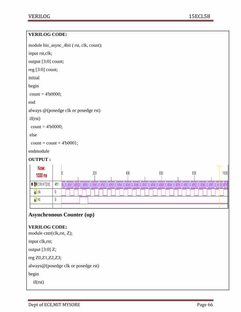
module bin_async_4bit ( rst, clk, count);
input rst,clk;
output [3:0] count;
reg [3:0] count;
initial
begin
count = 4'b0000;
end
always @(posedge clk or posedge rst)
if(rst)
count = 4'b0000;
else
count = count + 4'b0001;
endmodule
OUTPUT :
Asynchronous Counter (up)
VERILOG CODE: module cntr(clk,rst, Z);
input clk,rst;
output [3:0] Z;
reg Z0,Z1,Z2,Z3;
always@(posedge clk or posedge rst)
begin
if(rst)

VERILOG 15ECL58
Dept of ECE,MIT MYSORE Page 67
Z0=1'b1;
else
Z0=~Z0;
end
always@(negedge Z0 or posedge rst)
begin
if(rst)
Z1=1'b1;
else
Z1=~Z1;
end
always@(negedge Z1 or posedge rst)
begin
if(rst)
Z2=1'b1;
else
Z2=~Z2;
end
always@(negedge Z2 or posedge rst)
begin
if(rst)
Z3=1'b1;
else
Z3=~Z3;
end
assign Z={Z3,Z2,Z1,Z0};
endmodule OUTPUT :

VERILOG 15ECL58
Dept of ECE,MIT MYSORE Page 68
Asynchronous Counter (down) -VERILOG CODE:
module cntr(clk,rst, Z);
input clk,rst;
output [3:0] Z;
reg Z0,Z1,Z2,Z3;
always@(posedge clk or posedge rst)
begin
if(rst)
Z0=1'b1;
else
Z0=~Z0;
end
always@(posgedge Z0 or posedge rst)
begin
if(rst)
Z1=1'b1;
else
Z1=~Z1;
end
always@(posedge Z1 or posedge rst)
begin
if(rst)
Z2=1'b1;
else
Z2=~Z2;
end
always@(posedge Z2 or posedge rst)
begin
if(rst)
Z3=1'b1;
else Z3=~Z3;
end
assign Z={Z3,Z2,Z1,Z0};
endmodule

VERILOG 15ECL58
Dept of ECE,MIT MYSORE Page 69
OUTPUT:
6.2 BCD Synchronous Reset 4-bit Counter:
VERILOG CODE:
module bcd_sync ( rst, clk, count);
input rst,clk;
output [3:0] count;
reg [3:0] count;
initial
begin
count = 4'd0;
end
always @(posedge clk)
if(rst)
count = 4'd0;
else if(count < 4'd9 )
count = count + 4'd1;
else
count = 4'd0;
endmodule

VERILOG 15ECL58
Dept of ECE,MIT MYSORE Page 70
BCD Asynchronous Reset 4-bit Counter:
VERILOG CODE:
module bcd_async ( rst, clk, count);
input rst,clk;
output [3:0] count;
reg [3:0] count;
initial
begin
count = 4'd0;
end
always @(posedge clk or posedge rst)
if(rst)
count = 4'd0;
else if(count < 4'd9 )
count = count + 4'd1;
else
count = 4'd0;
endmodule

VERILOG 15ECL58
Dept of ECE,MIT MYSORE Page 71
OUTPUT:

VERILOG 15ECL58
Dept of ECE,MIT MYSORE Page 72
Binary Sequence (any) up down 4-bit Counter:
BLOCK DIAGRAM
VERILOG CODE:
module any_seq_bin ( rst,load, clk,din,updown, count);
input rst,clk,updown,load;
input [3:0] din;
output [3:0] count;
reg [3:0] count;
always @(posedge clk)
if(rst)
count = 4'b0000;
else if(load)
count = din;
else if (updown)
count = count + 4'b0001;
else
count = count - 4'b0001;
endmodule

VERILOG 15ECL58
Dept of ECE,MIT MYSORE Page 73
Probable Viva Questions:
1. Write short note on subprogram. 2. What are aliases? Explain with example. 3. Design and implement counter using VHDL which counts upto 9 and down
counts again from 9 to 0. 4. Differentiate between a process and wait statement. Can they be used simultaneously in a program? 5. What is the difference between variable and signal. 6. Write down the truth table and VHDL code for the 4-bit left to right shift register.
Also draw the circuit and output waveforms. 7. Write down the truth table and VHDL code for the 4-bit up/down counter. Also
draw the circuit and output waveforms 8. What are the basic components of a micro computer? Explain briefly. 9. Describe microcomputer implementation in VHDL. 10. How can a ROM be used as a PLA') Write down its advantages. 11. Discuss briefly 22 V /0 PLD. 12. Write short note on PAL 16L8. 13. Write short note on Various Loops in VHDL 14. Write short note on Packages.

VERILOG 15ECL58
Dept of ECE,MIT MYSORE Page 74
PART-B
INTERFACING PROGRAMS
1. 7 segment Display
(a) LED segments (b) Four displays with common anode and (c) LED connection on CPLD or FPGA Board.

VERILOG 15ECL58
Dept of ECE,MIT MYSORE Page 75
EXPERIMENT NO. 7
1. Write HDL code to display messages on the given seven segment display and
accepting Hex key pad as input data.
7-Segment display can display the digits 0-9 and the hex extension (A-F). A signal-character displays
bring out leads for 7-segments & the common elect code (Common cathode & common anode).Here in
FPGA/CPLD board to interface one 7-segment LED display whose elements are connected to any I/O
pins of the FPGA/CPLD. Here we can consider common-anode 7-segment LED displays. The user can
then ON by driving associated signal low.
--Keymatrix--
library IEEE;
use IEEE.STD_LOGIC_1164.ALL;
use IEEE.STD_LOGIC_ARITH.ALL;
use IEEE.STD_LOGIC_UNSIGNED.ALL;
entity segm is
Port ( clk : in STD_LOGIC;
a : out STD_LOGIC_VECTOR (7 downto 0));
end segm; architecture Behavioral of segm is
signal i: integer :=0;
signal sclk : STD_LOGIC_VECTOR (23 downto 0):="000000000000000000000000";
signal iclk: STD_LOGIC:='0';
begin
process (clk)
begin
if (clk ='1' and clk'event) then
sclk <= sclk+1;
end if;
end process;
iclk <= sclk(23);
process (iclk)

VERILOG 15ECL58
Dept of ECE,MIT MYSORE Page 76
begin
if (iclk ='1' and iclk'event) then
case i is
when 0 => a <= "11000000"; i <=1 ;
when 1 => a <= "11111001"; i <=2 ;
when 2 => a <= "10100100"; i <=3 ;
when 3 => a <= "10110000"; i <=4 ;
when 4 => a <= "10011001"; i <=5 ;
when 5 => a <= "10010010"; i <=6 ;
when 6 => a <= "10000010"; i <=7 ;
when 7 => a <= "11111000"; i <=8 ;
when 8 => a <= "10000000"; i <=9 ;
when 9 => a <= "10010000"; i <=0 ;
when others => null;
end case;
end if;
end process;
end Behavioral;
--keypad program--
library IEEE;
use IEEE.STD_LOGIC_1164.ALL;
use IEEE.STD_LOGIC_ARITH.ALL;
use IEEE.STD_LOGIC_UNSIGNED.ALL; entity keypad is
Port ( row : inout STD_LOGIC_VECTOR (3 downto 0);
col : in STD_LOGIC_VECTOR (3 downto 0); clk : in STD_LOGIC; a : out STD_LOGIC_VECTOR (7 downto 0));
end keypad; architecture Behavioral of keypad is
signal row1 : STD_LOGIC_VECTOR (3 downto 0):="0111";
begin
process (clk)
begin

VERILOG 15ECL58
Dept of ECE,MIT MYSORE Page 77
if (clk='1' and clk'event) then
row1 <= row1(2 downto 0) & row1 (3);
end if;
end process;
row <= row1;
process (clk)
begin
if (clk='1' and clk'event) then
if (row1= "0111" and col ="0111") then a <= "11000000"; elsif
(row1= "0111" and col ="1011") then a <= "11111001"; elsif
(row1= "0111" and col ="1101") then a <= "10100100"; elsif
(row1= "0111" and col ="1110") then a <= "10110000";
elsif (row1= "1011" and col ="0111") then a <= "10011001";
elsif (row1= "1011" and col ="1011") then a <= "10010010";
elsif (row1= "1011" and col ="1101") then a <= "10000010";
elsif (row1= "1011" and col ="1110") then a <= "11111000";
elsif (row1= "1101" and col ="0111") then a <= "10000000";
elsif (row1= "1101" and col ="1011") then a <= "10010000";
elsif (row1= "1101" and col ="1101") then a <= "10001000";
elsif (row1= "1101" and col ="1110") then a <= "10000011";
elsif (row1= "1110" and col ="0111") then a <=
"11000110"; elsif (row1= "1110" and col ="1011") then a
<= "11000000"; elsif (row1= "1110" and col ="1101") then
a <= "10000110"; elsif (row1= "1110" and col ="1110")
then a <= "10001110"; else a<= "11111111";
end if; end if;
end process;
end Behavioral;

VERILOG 15ECL58
Dept of ECE,MIT MYSORE Page 78
--HELP DISPLAY--
library IEEE;
use IEEE.STD_LOGIC_1164.ALL;
use IEEE.STD_LOGIC_ARITH.ALL;
use IEEE.STD_LOGIC_UNSIGNED.ALL; entity he is
Port ( clk : in STD_LOGIC;
sel : out STD_LOGIC_VECTOR (3 downto 0);
a: out STD_LOGIC_VECTOR (7 downto 0));
end he;
architecture Behavioral of he is
signal i: integer :=0;
signal delay : STD_LOGIC_VECTOR (3 downto 0);
begin
process (clk)
begin
if (clk ='1' and clk'event) then
delay <= delay + 1;
end if;
end process;
process (delay(3))
begin
if (rising_edge (delay(3))) then
case i is
when 0 => a <= "10001001"; i <=1; sel<="0111";
when 1 => a <= "10000110"; i <=2; sel<="1011";
when 2 => a <= "11000111"; i <=3; sel<="1101";
when 3 => a <= "10001100"; i <=0; sel<="1110"; when others => null;
end case;
end if;
end process;
end Behavioral;

VERILOG 15ECL58
Dept of ECE,MIT MYSORE Page 79
2 STEPPER MOTOR AND DC MOTOR:
Stepper Motor:
A stepper motor is a digital motor. It can be driven by digital signal. The motor has two phase with
center tap winding. The centre taps of these windings are connected to the 12V supply. Due to this
motor can be excited by grounding four terminals of the two windings. Motor can be rotated in steps by giving proper excitation to these windings. These excitation signals are
buffered using transistor. The transistors are selected such that they can source the stored current for the
windings.Motor is rotated by 1.8 degree per excitation. Speed can be changed by varying the clock.
DC Motor:
A DC motor is any of a class of rotary electrical machines that converts direct current electrical energy
into mechanical energy. The most common types rely on the forces produced by magnetic fields. Nearly
all types of DC motors have some internal mechanism, either electromechanical or electronic, to
periodically change the direction of current flow in part of the motor.

VERILOG 15ECL58
Dept of ECE,MIT MYSORE Page 80
EXPERIMENT NO. 8
VHDL Code to rotate Stepper Motor in Clockwise direction :
library IEEE;
use IEEE.STD_LOGIC_1164.ALL;
use IEEE.STD_LOGIC_ARITH.ALL;
use IEEE.STD_LOGIC_UNSIGNED.ALL;
entity stmo is
Port ( clk : in STD_LOGIC;
q : out STD_LOGIC_VECTOR (3 downto 0));
end stmo; architecture Behavioral of stmo is
signal delay:STD_LOGIC_VECTOR (15 downto
0):="0000000000000000"; signal da:STD_LOGIc; signal a:STD_LOGIC_VECTOR (3 downto 0):="1110";
begin
process(clk)
begin
if (clk='1' and clk'event) then
delay <= delay+1;
end if;
end process;
da<= delay(15);
process(da)
begin
if( rising_edge (da)) then
a<= a( 0) & a(3 downto 1);
end if ;
end process;
q<= a;
end Behavioral;

VERILOG 15ECL58
Dept of ECE,MIT MYSORE Page 81
VHDL Code to rotate Stepper Motor in Anticlockwise direction :
library IEEE;
use IEEE.STD_LOGIC_1164.ALL;
use IEEE.STD_LOGIC_ARITH.ALL;
use IEEE.STD_LOGIC_UNSIGNED.ALL;
entity stmo is
Port ( clk : in STD_LOGIC;
q : out STD_LOGIC_VECTOR (3 downto 0));
end stmo; architecture Behavioral of stmo is
signal delay:STD_LOGIC_VECTOR (15 downto
0):="0000000000000000"; signal da:STD_LOGIc; signal a:STD_LOGIC_VECTOR (3 downto 0):="1110";
begin
process(clk)
begin
if (clk='1' and clk'event) then
delay <= delay+1;
end if;
end process;
da<= delay(15);
process(da)
begin
if( rising_edge (da)) then
a<= a(2 downto 0) & a(3);
end if ;
end process;
q<= a;
end Behavioral;

VERILOG 15ECL58
Dept of ECE,MIT MYSORE Page 82
VHDL Code to rotate Stepper Motor Clockwise for finite number of steps-100 steps or
180o:
library IEEE; use IEEE.STD_LOGIC_1164.ALL;
use IEEE.STD_LOGIC_ARITH.ALL;
use IEEE.STD_LOGIC_UNSIGNED.ALL; entity stmo1 is
Port ( clk : in STD_LOGIC;
q : out STD_LOGIC_VECTOR (3 downto 0));
end stmo1;
architecture Behavioral of stmo1 is
signal delay:STD_LOGIC_VECTOR (15 downto 0):="0000000000000000";
signal da:STD_LOGIC;
signal I : STD_LOGIC_VECTOR (7 downto 0);
signal a:STD_LOGIC_VECTOR (3 downto 0):="1110";
begin
process(clk)
begin
if (clk='1' and clk'event) then
delay <= delay+1;
end if;
end process;
da<= delay(15);
process(da)
begin
if( rising_edge (da)) then
a<= a( 0) & a(3 downto 1);
I <= i+1;
end if;
If (i= “01100100”) then a <= “1111”;
end if;
q<= a;
end process;
end Behavioral;

VERILOG 15ECL58
Dept of ECE,MIT MYSORE Page 83
VHDL Code to rotate Stepper Motor Clockwise-100 steps and then Anticlockwise -100
steps( i.e 180o each) :
library IEEE;
use IEEE.STD_LOGIC_1164.ALL;
use IEEE.STD_LOGIC_ARITH.ALL;
use IEEE.STD_LOGIC_UNSIGNED.ALL;
entity stmo1 is
Port ( clk : in STD_LOGIC;
q : out STD_LOGIC_VECTOR (3 downto 0));
end stmo1; architecture Behavioral of stmo1 is
signal delay:STD_LOGIC_VECTOR (15 downto 0) ;
signal a:STD_LOGIC_VECTOR (3 downto 0):="1110";
signal da:STD_LOGIC;
signal i : integer :=0;
begin
process(clk)
begin
if (clk='1' and clk'event) then
delay <= delay+1;
end if;
end process;
da<= delay(15);
process(da)
begin
if( rising_edge (da)) then
if (i<100) then

VERILOG 15ECL58
Dept of ECE,MIT MYSORE Page 84
a<= a( 0) & a(3 downto 1);
elsif (i>100 & i< 200) then
a <= a(2 downto 0) & a(3);
elsif (i>200) then
a<= “1111”;
end if;
i <= i+1;
end if;
end process;
q<= a;
i <= i+1;
end Behavioral;
DC MOTOR
Write HDL code to control speed, direction of DC motor.
library IEEE;
use IEEE.STD_LOGIC_1164.ALL;
use IEEE.STD_LOGIC_ARITH.ALL;
use IEEE.STD_LOGIC_UNSIGNED.ALL;
entity dc_motor is
Port ( clk : in STD_LOGIC;
psw : in STD_LOGIC_vector(2 downto 0);
pdcm : out STD_LOGIC );
end dc_motor;
architecture Behavioral of dc_motor is

VERILOG 15ECL58
Dept of ECE,MIT MYSORE Page 85
signal sclk_div : std_logic_vector(11 downto 0) := “000000000000”;
signal da : std_logic;
begin
process(clk)
begin
if(rising_edge(clk)) then
sclk_div <= sclk_div + '1' ;
end if;
da <= sclk_div (11);
if ( sclk_div = “101110111000” ) then
sclk_div <= “000000000000”;
end if;
end process;
process(psw, da)
variable vdcm : std_logic;
begin
if ( sclk_div = “000000000000” ) then
vdcm:= ‘1’;
end if;
if (psw = “000” and sclk_div = “000111110100”) then vdcm:=’0’;
elsif (psw = “001” and sclk_div = “001100100000”) then vdcm:=’0’;
elsif (psw = “010” and sclk_div = “010001001100”) then vdcm:=’0’;
elsif (psw = “011” and sclk_div = “010101111000”) then vdcm:=’0’;
elsif (psw = “100” and sclk_div = “011010100100”) then vdcm:=’0’;
elsif (psw = “101” and sclk_div = “011111010000”) then vdcm:=’0’;
elsif (psw = “110” and sclk_div = “100011111100”) then vdcm:=’0’;
elsif (psw = “111” and sclk_div = “100111000100”) then vdcm:=’0’;
end if;
if (vdcm=’1’) then pdcm <= ‘1’;
else pdcm <= ‘0’;
end if;
end process;
end behavioral;

VERILOG 15ECL58
Dept of ECE,MIT MYSORE Page 86
--TESTCOUNT library IEEE;
use IEEE.STD_LOGIC_1164.ALL;
use IEEE.STD_LOGIC_ARITH.ALL;
use IEEE.STD_LOGIC_UNSIGNED.ALL;
entity testcnt is
Port ( clk : in std_logic; one : out std_logic); end
testcnt;
architecture Behavioral of testcnt is
signal cnt : std_logic_vector(7 downto 0):="00000000";
signal check: std_logic:='0';
signal t: std_logic:='0';
begin
tenm:process(clk)
begin
if (clk'event and clk ='1') then cnt <= cnt + '1';
if cnt = "0011001" then check <= not check; cnt <= "00000000";
end if;
end if;
end process tenm;
onek:process(check)
begin
if check'event and check = '1'
then t <= not t;
one <= t;
end if;
end process onek;
end Behavioral;

VERILOG 15ECL58
Dept of ECE,MIT MYSORE Page 87
DAC:
EXPERIMENT NO.9
Write HDL code to generate different waveforms (Sine, Square, Triangle,
Ramp etc.,) using DAC (change the frequency and amplitude).
i) Digital to analog converter (square wave generation)
library IEEE;
use IEEE.STD_LOGIC_1164.ALL;
use IEEE.STD_LOGIC_ARITH.ALL;
use IEEE.STD_LOGIC_UNSIGNED.ALL;
entity sq is
Port ( clk : in STD_LOGIC;
dout : out STD_LOGIC_VECTOR (7 downto 0));
end sq;
architecture Behavioral of sq is
signal delay : STD_LOGIC_VECTOR (15 downto 0):="0000000000000000";
begin
Process (clk)
begin
if (clk='1' and clk'event) then
delay <= delay+1;
end if;
if ( delay(15)= '1' )then

VERILOG 15ECL58
Dept of ECE,MIT MYSORE Page 88
dout <= "11111111";
else
dout <= "00000000";
end if;
end process;
end Behavioral;
ii) Digital to analog converter (Generation of Ramp)
library ieee ;
use ieee.std_logic_1164.all ;
use ieee.std_logic_arith.all ;
use ieee.std_logic_unsigned.all ;
entity ramp is
port (clk, rst : in std_logic ;
dac_out : out std_logic_vector (11 downto 0));
end ramp ;
architecture beh of ramp is
signal count : std_logic_vector (11 downto 0);
begin
process(clk, rst)
begin
if (rst = ‘1’) then count < =(others => ‘0’);
elsif (clk’ event and clk = ‘1’)then
count < =count +1;
end if;
end process;
dac_out < = count;
end beh;

VERILOG 15ECL58
Dept of ECE,MIT MYSORE Page 89
iii) Digital to analog converter (Generation of triangle wave)
library IEEE;
use IEEE.STD_LOGIC_1164.ALL;
use IEEE.STD_LOGIC_ARITH.ALL;
use IEEE.STD_LOGIC_UNSIGNED.ALL;
entity tria is
Port ( clk : in STD_LOGIC;
dout : out STD_LOGIC_VECTOR (7 downto 0));
end tria; architecture Behavioral of tria is
signal count: STD_LOGIC_VECTOR (7 downto 0) := "00000000";
signal count1: STD_LOGIC := '0';
begin
process (clk)
begin
if (clk = '1' and clk'event) then
if (count1='0') then
count <= count+1;
elsif (count1='1') then
count <= count-1;
end if;
end if;
end process;
dout <= count;
process (clk)
begin
if (clk = '1' and clk'event) then
if (count="11111110") then count1 <='1';

VERILOG 15ECL58
Dept of ECE,MIT MYSORE Page 90
elsif (count="00000001") then count1 <='0';
end if;
end if;
end process;
end Behavioral;
iv) Digital to analog converter (Generation of sine wave)
library IEEE;
use IEEE.STD_LOGIC_1164.ALL;
use IEEE.STD_LOGIC_ARITH.ALL;
use IEEE.STD_LOGIC_UNSIGNED.ALL;
entity sin is
Port ( clk : in STD_LOGIC;
z : out STD_LOGIC_VECTOR (7 downto 0));
end sin; architecture Behavioral of sin is
signal a : STD_LOGIC_VECTOR (7 downto 0);
signal i: integer :=0;
begin
process (clk)
type sinewave is array (0 to 35) of STD_LOGIC_VECTOR (7 downto 0);
constant sine :sinewave :=("36 values"); --use formula (128+128sinθ) to calculate 36 values
begin if (clk='1' and clk'event) then
a <= sine(i);
i <= i+1;
if (i = 36) then i <= 0;
end if;
end if;
end process;
z <= a;
end Behavioral;

VERILOG 15ECL58
Dept of ECE,MIT MYSORE Page 91
VHDL Code to generate SQUARE AND TRIANGULAR WAVES alternatively:
entity sqtri is
port (clk : in std_logic;
z : out std_logic_vector (7 downto 0));
end sqtri;
architecture behave of sqtri is
signal I : integer := 0;
signal a: std_logic_vector (7 downto 0) := “00000000”;
begin
process (clk)
begin
if (clk = ‘1’ and clk’event) then
if ( i >=0 and i<256) then
a <= “11111111”;
i <= i+1;
elsif (i>256 and i<512) then
a <= “00000000”;
i<=i+1;
elsif (i>=512 and i<768) then
a<= a+1;
i<=i+1;
elsif (i>=768 and i<1024) then
a<= a-1;
i<=i+1;
end if;
if (i=1024) then i<=0;
end if;
end if;
end process;
z<=a;
end behave;

VERILOG 15ECL58
Dept of ECE,MIT MYSORE Page 92
EXPERIMENT NO. 10
Write VHDL code to simulate Elevator operations
An elevator is a transport device used to move goods or people vertically outside. Elevators are also
called as lifts. An elevator is essentially a platform that is either pulled or pushed up by a mechanical
means. A modern day elevator consists of a cab mounted on a platform with an enclose space called a
“noistway”. In the past, elevator drive mechanisms were powered by stream and water hydraulic pistons.
In “traction” elevator, cars are pulled by means of rolling steel ropes over a deeply grooved pully,
commonly called a sheave in the industry. The weight of car is balanced with a counter weight. Sometimes two always move synchronously in
opposite directions and they are each other’s counter weight.
library IEEE;
use IEEE.STD_LOGIC_1164.ALL;
use IEEE.STD_LOGIC_ARITH.ALL;
use IEEE.STD_LOGIC_UNSIGNED.ALL;
entity elevator is
Port ( pclk100k : in std_logic ;
pkeyret : in std_logic_vector(3 downto 0);
pkeyscn : out std_logic_vector(3 downto 0) ;
opled : out std_logic_vector(3 downto 0);
pdspseg: out std_logic_vector (3 downto 0) );
end elevator;
architecture behavioral of elevator is
type l_state is ( check, ready, analys, azine, derive, feature, operating,
arrived); signal present_state : l_state;
signal sclkdiv : std_logic_vector(15 downto 0):= "0000000000000000";
signal skeyclk : std_logic;
signal led_no : integer range 0 to 11 := 0 ;
signal skeyscn : std_logic_vector(3 downto 0) := "1110";

VERILOG 15ECL58
Dept of ECE,MIT MYSORE Page 93
signal lkeyret : std_logic_vector(3 downto 0);
signal lkeyscn : std_logic_vector(3 downto 0) := "1110"; signal
pkeyret2 : std_logic_vector(3 downto 0):= "1110" ; type tseg7
is array(0 to 11) of std_logic_vector (3 downto 0);
signal tempseg: tseg7 := ("0000","0000","0000","0000","0000", "0000","0000","0000",
"0000","0000","0000","0000");
signal skeyhit : std_logic;
signal skeyflr : integer range 0 to 15 := 0;
begin
process(pclk100k, sclkdiv)
begin
if( rising_edge(pclk100k)) then
sclkdiv <= sclkdiv+1;
end if;
skeyclk <= sclkdiv(15);
end process;
process (skeyclk, led_no)
begin
if( rising_edge(skeyclk)) then
case led_no is
when 0 => opled <= "0001";
when 1 => opled <= "0010";
when 2 => opled <= "0011";
when 3 => opled <= "0100";
when 4 => opled <= "0101";
when 5 => opled <= "0110";
when 6 => opled <= "0111";
when 7 => opled <= "1000";
when 8 => opled <= "1001";
when 9 => opled <= "1010" ;
when 10 => opled <= "1011";

VERILOG 15ECL58
Dept of ECE,MIT MYSORE Page 94
when 11 => opled <= "1100";
when others => opled <= "1101";
end case;
end if;
end process;
process (skeyclk)
begin
if( rising_edge(skeyclk)) then
case present_state is
when check =>
if pkeyret2 /= pkeyret
present_state <= ready;
pkeyscn <= skeyscn;
skeyscn <= "1111";
else pkeyret2 <= pkeyret;
end if;
when ready =>
pkeyscn <= skeyscn;
lkeyret <= pkeyret ;
present_state <= analys;
when analys =>
pkeyret2 <= pkeyret;
present_state <= azine;
when azine =>
then
case pkeyret2 is
when "1110" => skeyhit <= '1';
when "1101" => skeyhit <= '1';
when "1011" => skeyhit <= '1';
when "0111" => skeyhit <= '1';
when others => skeyhit <= '0';
end case;

VERILOG 15ECL58
Dept of ECE,MIT MYSORE Page 95
present_state <= derive;
when derive =>
if skeyhit = '0' then
present_state <= arrived;
skeyscn <= "0000";
else
if(lkeyscn = "1110" and lkeyret = "1110")
then skeyflr <= 0;
elsif(lkeyscn = "1110" and lkeyret = "1101")
then skeyflr <= 1;
elsif(lkeyscn = "1110" and lkeyret = "1011")
then skeyflr <= 2;
elsif(lkeyscn = "1110" and lkeyret = "0111")
then skeyflr <= 3;
elsif(lkeyscn = "1101" and lkeyret = "1110")
then skeyflr <= 4;
elsif(lkeyscn = "1101" and lkeyret = "1101")
then skeyflr <= 5;
elsif(lkeyscn = "1101" and lkeyret = "1011")
then skeyflr <= 6;
elsif(lkeyscn = "1101" and lkeyret = "0111")
then skeyflr <= 7;
elsif(lkeyscn = "1011" and lkeyret = "1110")
then skeyflr <= 8;
elsif(lkeyscn = "1011" and lkeyret = "1101")
then skeyflr <= 9;
elsif(lkeyscn = "1011" and lkeyret = "1011")
then skeyflr <= 10;
elsif(lkeyscn = "1011" and lkeyret = "0111")
then skeyflr <= 11;

VERILOG 15ECL58
Dept of ECE,MIT MYSORE Page 96
elsif(lkeyscn = "0111" and lkeyret = "1110")
then skeyflr <= 12;
elsif(lkeyscn = "0111" and lkeyret = "1101")
then skeyflr <= 13;
elsif(lkeyscn = "0111" and lkeyret = "1011")
then skeyflr <= 14;
elsif(lkeyscn = "0111" and lkeyret = "0111")
then skeyflr <= 15;
--
end if;
present_state <= feature ;
end if;
when feature =>
present_state <= operating ;
case skeyflr is
when 0 => tempseg <=
("0000","0000","0001","0010","0011","0100","0101","0110","0111","1000","1001","0111");
when 0 => tempseg <= ("0000","0000","0000","0000","0000","0000","0000","0000","0000","0000","0000","1110");
when 1 => tempseg <= ("0000","0000","0001","0010","0011","0011","0011","0011","0011","0011","0011","1101");
when 2 => tempseg <= ("0000","0000","0001","0010","0011","0100","0101","0110","0110","0110","0110","1011");
when 3 => tempseg <= ("0000","0000","0001","0010","0011","0100","0101","0110","0111","1000","1001","0111");
when 4 => tempseg <= ("0011","0011","0010","0001","0000","0000","0000","0000","0000","0000","0000","1110");
when 5 => tempseg <= ("0011","0011","0011","0011","0011","0011","0011","0011","0011","0011","0011","1101");
when 6 => tempseg <= ("0011","0011","0100","0101","0110","0110","0110","0110","0110","0110","0110","1011");

VERILOG 15ECL58
Dept of ECE,MIT MYSORE Page 97
when 7 => tempseg <=
("0011","0011","0100","0101","0110","0111","1000","1001","1001","1001","1001","0111");
when 8 => tempseg <=
("0110","0110","0101","0100","0011","0010","0001","0000","0000","0000","0000","1110");
when 9 => tempseg <=
("0110","0110","0101","0100","0011","0011","0011","0011","0011","0011","0011","1101");
when 10 => tempseg <=
("0110","0110","0110","0110","0110","0110","0110","0110","0110","0110","0110","1011");
when 11 => tempseg <=
("0110","0110","0111","1000","1001","1001","1001","1001","1001","1001","1001","0111");
when 12 => tempseg <=
("1001","1001","1000","0111","0110","0101","0100","0011","0010","0001","0000","1110");
when 13 => tempseg <=
("1001","1001","1000","0111","0110","0101","0100","0011","0011","0011","0011","1101");
when 14 => tempseg <=
("1001","1001","1000","0111","0110","0110","0110","0110","0110","0110","0110","1011");
when 15 => tempseg <=
("1001","1001","1001","1001","1001","1001","1001","1001","1001","1001","1001","0111");
end case;
when
operating => pdspseg <= tempseg(led_no);
led_no <= led_no + 1;
if
led_no = 10
then
present_state <= arrived;
end if;
when
arrived => pdspseg <= tempseg(10);
led_no <= 0 ;
lkeyscn <= tempseg(11);
skeyscn <= tempseg(11);
present_state <= check; end case;
end if;
end process;
end behavioral;

VERILOG 15ECL58
Dept of ECE,MIT MYSORE Page 98
Note: The Pin numbers in User Constraints File (UCF) depends on the Fringe Ribbon Cables (FRCs) used for inputs & outputs as well as the devices selected during the project creation. So these pin numbers are not fixed.
Model Viva Questions:
1. What does VHDL stands for?
2. Which IEEE standard describes the VHDL language?
3. List the three popular Hardware languages.
4. Which are the different levels of abstraction that can be specified using VHDL?
5. List the different design units of VHDL.
6. Which are the mandatory design units to write VHDL code?
7. Which are the different modes of port declaration?
8. Which are the valid characters for identifier declaration?
9. Which are the different classes of operators?
10. Where do you write the concurrent statements?
11. Where do you write the sequential statement?
12. In which model process statement appears?
13. What is the importance of sensitivity list in process statement?
14. Is VHDL Case sensitive?
15. Does VHDL support multi dimensional arrays?
16. Can combinational circuits be coded inside the process?
17. Does VHDL support operator overloading?
18. Is it possible to write multiple entities for a single architecture?
19. Is it possible to write multiple architectures for a single entity?
20. Where we declare the variable?
21. Write device configuration for CPLD and FPGA Used in your Lab.
22. Expand CPLD and FPGA.
23. Differentiate sequential and concurrent statement.
24. List the different types of wait statements.
25. How you model your program using wait statement?
26. What are the different modeling styles in VHDL?
27. What is the difference between the bit and std_logic?

VERILOG 15ECL58
Dept of ECE,MIT MYSORE Page 99
28. What is the difference between the variable and signals?
29. Name the different VHDL objects.
30. Name the different data types used in VHDL.
31. Explain the VHDL term (i) Entity, (ii) Architecture, (iii) Configuration, (iv) Package,
(v) Driver, (vi) Process, (vii) Attribute, (viii) Generic and (ix) Bus.
32. Write the general syntax for Case, LOOP, Architecture Configuration, package, Process, Exit.
33. Differentiate between Procedure and Function
34. Explain attribute, event, range
35. How to detect signal edge using attribute?
36. What is synthesis?
37. What is simulation?
38. Differentiate between syntax error and semantic error.
39. Is other clause necessary in VHDL case statement? why?
40. What are the inputs required for synthesis?
41. Which architecture description you preferred? Why?
42. Which Tool you used for simulation?
43. Which Tool you used for synthesis?
44. Xc3s400tq144-4
what 3S stands for? What 400 stand for? What tq144 stands for?
45. Xc3s400tq144-4
what xc stands for? what -4 stands for? 46. What is the difference between CPLD and FPGA?
47. What is the difference between synchronous and asynchronous reset?
48. What is the basic element of memory?
49. What do you mean by latch?
50. How you model latch in VHDL?
51. What is the difference between synchronous and asynchronous counter?
52. What is the difference between backend and front-end?
53. Expand ASIC.
54. Expand JTAG.
55. Expand ISE
56. Which IEEE standard supports JTAG?
57. What information is present in .Bit File?
58. What do you mean by configuration?
59. Which file used to configure the CPLD?
60. Which file used to configure the FPGA?