Introduction to CMOS VLSI Design Sequential Circuits
52
Introduction to CMOS VLSI Design Sequential Circuits
description
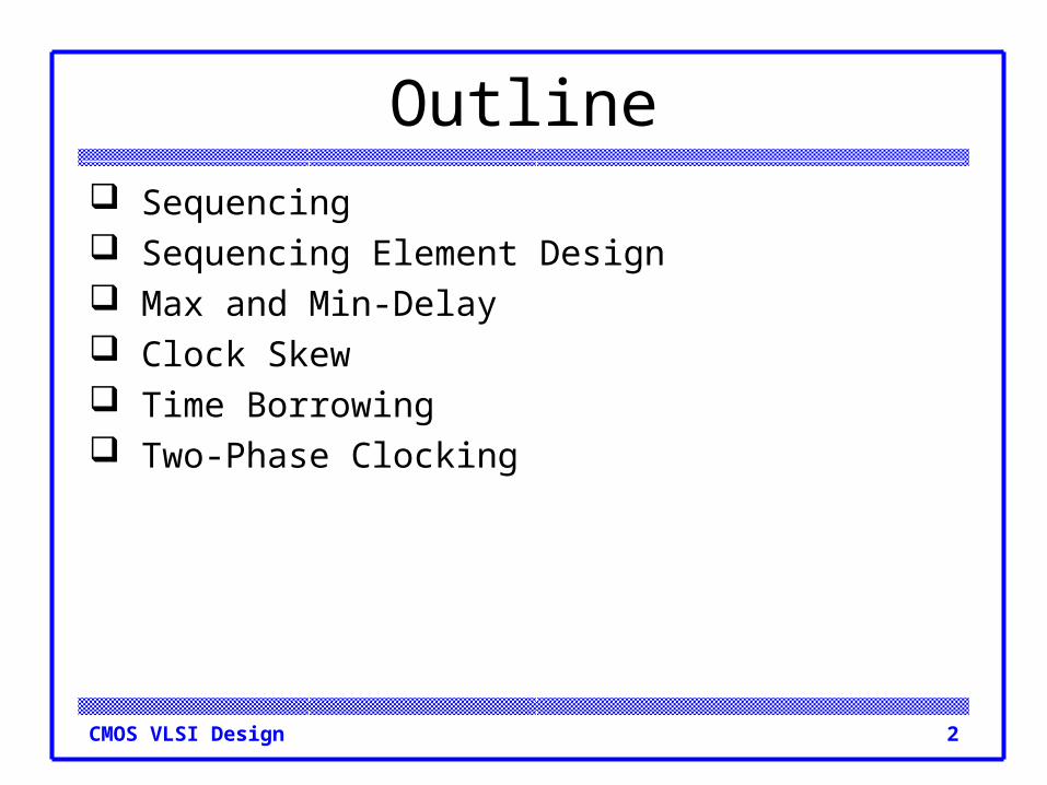
Introduction to CMOS VLSI Design Sequential Circuits. Outline. Sequencing Sequencing Element Design Max and Min-Delay Clock Skew Time Borrowing Two-Phase Clocking. Sequencing. Combinational logic output depends on current inputs Sequential logic - PowerPoint PPT Presentation
Transcript of Introduction to CMOS VLSI Design Sequential Circuits
Introduction toCMOS VLSI
Design
Sequential Circuits
2CMOS VLSI Design
Outline Sequencing Sequencing Element Design Max and Min-Delay Clock Skew Time Borrowing Two-Phase Clocking

3CMOS VLSI Design
Sequencing Combinational logic
– output depends on current inputs Sequential logic
– output depends on current and previous inputs– Requires separating previous, current, future– Called state or tokens– Ex: FSM, pipeline
CL
clk
in out
clk clk clk
CL CL
PipelineFinite State Machine
4CMOS VLSI Design
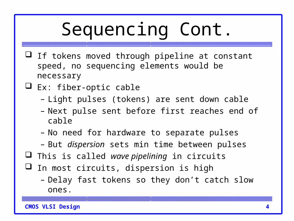
Sequencing Cont. If tokens moved through pipeline at constant speed,
no sequencing elements would be necessary Ex: fiber-optic cable
– Light pulses (tokens) are sent down cable– Next pulse sent before first reaches end of cable– No need for hardware to separate pulses– But dispersion sets min time between pulses
This is called wave pipelining in circuits In most circuits, dispersion is high
– Delay fast tokens so they don’t catch slow ones.

5CMOS VLSI Design
Sequencing Overhead Use flip-flops to delay fast tokens so they move
through exactly one stage each cycle. Inevitably adds some delay to the slow tokens Makes circuit slower than just the logic delay
– Called sequencing overhead Some people call this clocking overhead
– But it applies to asynchronous circuits too– Inevitable side effect of maintaining sequence
6CMOS VLSI Design
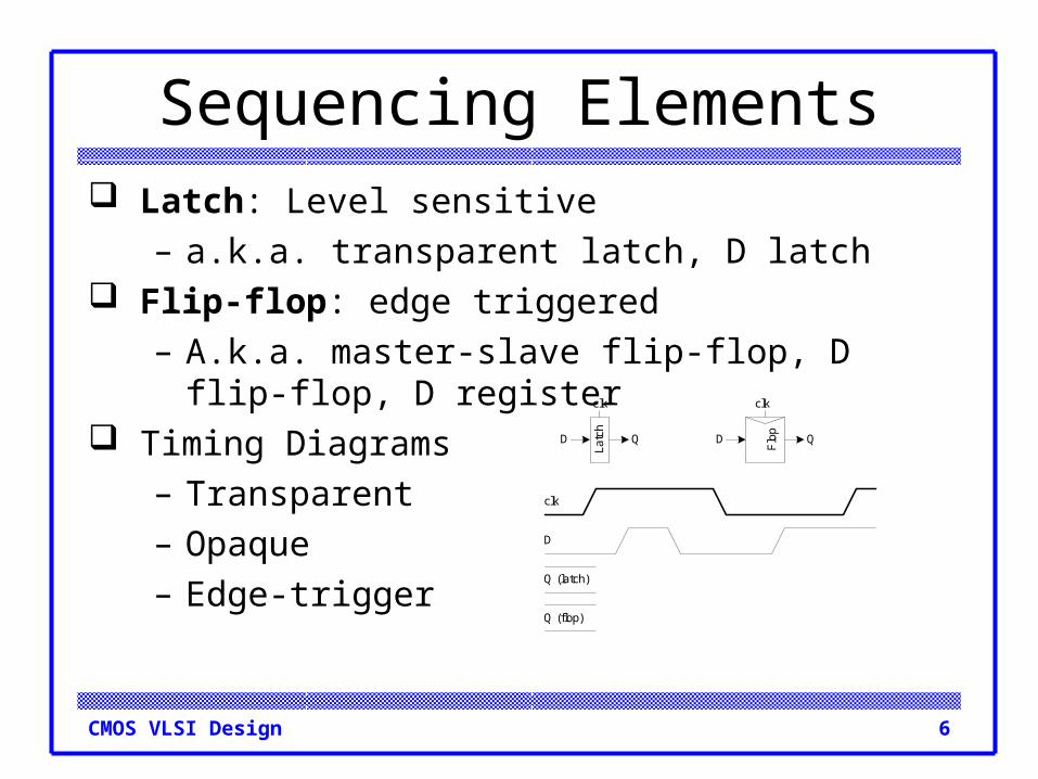
Sequencing Elements Latch: Level sensitive
– a.k.a. transparent latch, D latch Flip-flop: edge triggered
– A.k.a. master-slave flip-flop, D flip-flop, D register Timing Diagrams
– Transparent– Opaque– Edge-trigger
D
Flop
Latc
h
Q
clk clk
D Q
clk
D
Q (latch)
Q (flop)
7CMOS VLSI Design
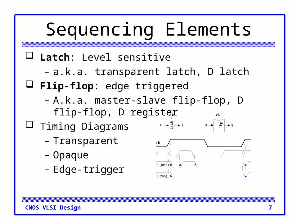
Sequencing Elements Latch: Level sensitive
– a.k.a. transparent latch, D latch Flip-flop: edge triggered
– A.k.a. master-slave flip-flop, D flip-flop, D register Timing Diagrams
– Transparent– Opaque– Edge-trigger
D
Flop
Latc
h
Q
clk clk
D Q
clk
D
Q (latch)
Q (flop)

8CMOS VLSI Design
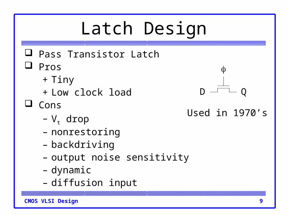
Latch Design Pass Transistor Latch Pros
+ +
Cons– – – – – –
D Q
9CMOS VLSI Design
Latch Design Pass Transistor Latch Pros
+ Tiny+ Low clock load
Cons– Vt drop– nonrestoring– backdriving– output noise sensitivity– dynamic– diffusion input
D Q
Used in 1970’s
10CMOS VLSI Design
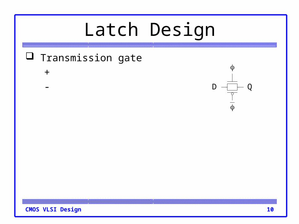
Latch Design Transmission gate
+ - D Q

11CMOS VLSI Design
Latch Design Transmission gate
+ No Vt drop
- Requires inverted clock D Q
12CMOS VLSI Design
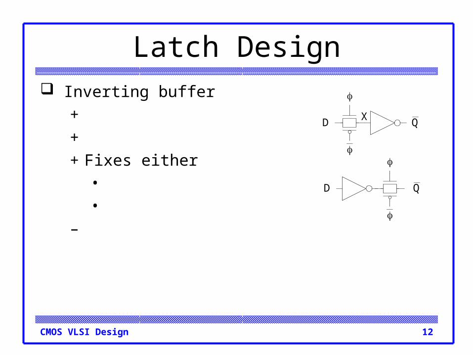
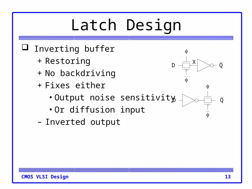
Latch Design Inverting buffer
+ + + Fixes either
• •
–
D
X Q
D Q
13CMOS VLSI Design
Latch Design Inverting buffer
+ Restoring+ No backdriving+ Fixes either
• Output noise sensitivity• Or diffusion input
– Inverted output
D
X Q
D Q

14CMOS VLSI Design
Latch Design Tristate feedback
+ –
QD X

15CMOS VLSI Design
Latch Design Tristate feedback
+ Static– Backdriving risk
Static latches are now essential
QD X
16CMOS VLSI Design
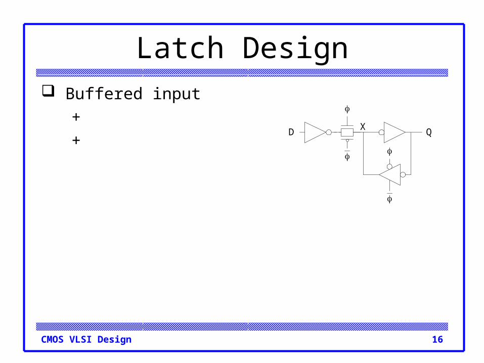
Latch Design Buffered input
+ +
QD X
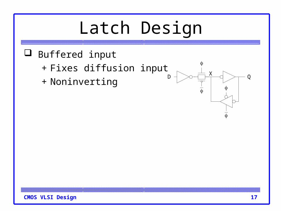
17CMOS VLSI Design
Latch Design Buffered input
+ Fixes diffusion input+ Noninverting
QD X

18CMOS VLSI Design
Latch Design Buffered output
+
Q
D X
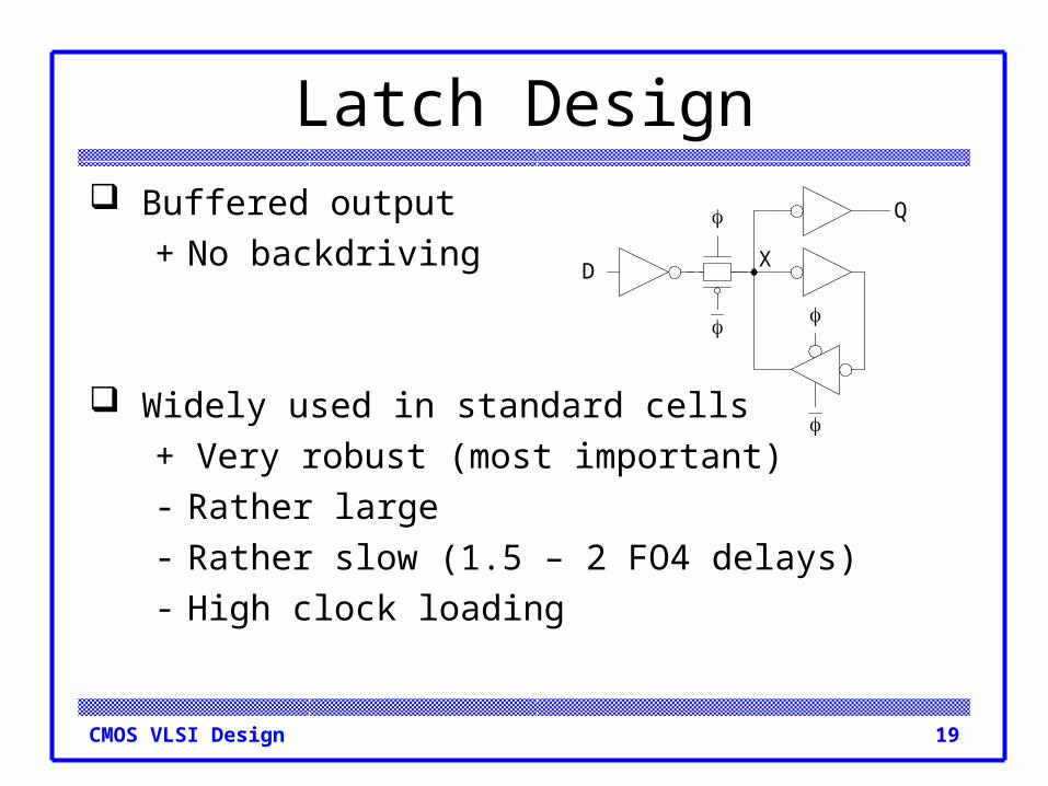
19CMOS VLSI Design
Latch Design Buffered output
+ No backdriving
Widely used in standard cells+ Very robust (most important)- Rather large- Rather slow (1.5 – 2 FO4 delays)- High clock loading
Q
D X
20CMOS VLSI Design
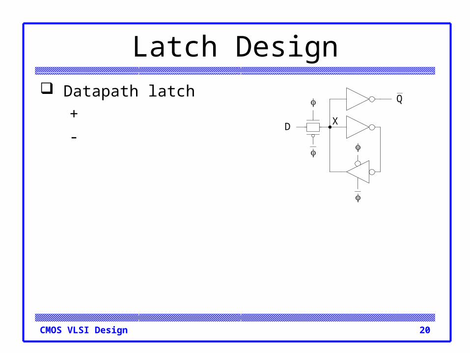
Latch Design Datapath latch
+ -
Q
D X

21CMOS VLSI Design
Latch Design Datapath latch
+ Smaller, faster- unbuffered input
Q
D X

22CMOS VLSI Design
Flip-Flop Design Flip-flop is built as pair of back-to-back latches
D Q
X
D
X
Q
Q

23CMOS VLSI Design
Enable Enable: ignore clock when en = 0
– Mux: increase latch D-Q delay– Clock Gating: increase en setup time, skew
D Q
Latc
h
D Q
en
en
Latc
hDQ
0
1
en
Latc
h
D Q
en
DQ
0
1
enD Q
en
Flop
Flop
Flop
Symbol Multiplexer Design Clock Gating Design
24CMOS VLSI Design
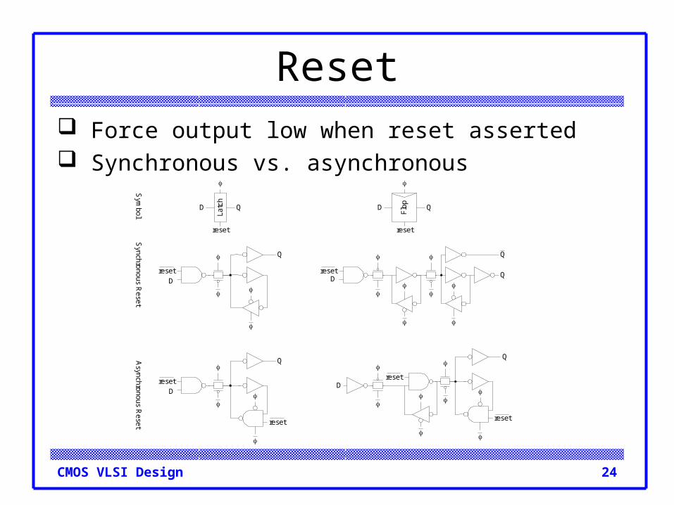
Reset Force output low when reset asserted Synchronous vs. asynchronous
D
Q
Q
reset
D
Q
Dreset
Q
Dreset
reset
reset
Synchronous R
esetA
synchronous Reset
Sym
bol FlopD Q
Latc
h
D Q
reset reset
Q
reset

25CMOS VLSI Design
Set / Reset Set forces output high when enabled
Flip-flop with asynchronous set and reset
D
Q
reset
set reset
set
26CMOS VLSI Design
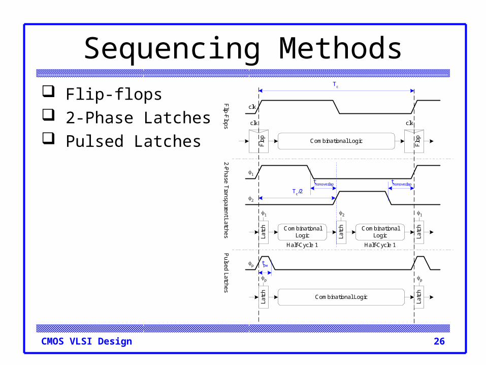
Sequencing Methods Flip-flops 2-Phase Latches Pulsed Latches
Flip-FlopsFl
opLa
tch
Flop
clk
1
2
p
clk clk
Latc
h
Latc
h
p p
1 12
2-Phase Transparent Latches
Pulsed Latches
Combinational Logic
CombinationalLogic
CombinationalLogic
Combinational Logic
Latc
h
Latc
h
Tc
Tc/2
tnonoverlap tnonoverlap
tpw
Half-Cycle 1 Half-Cycle 1
27CMOS VLSI Design
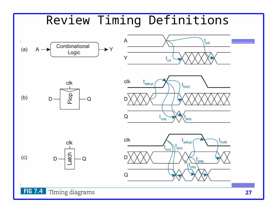
Review Timing Definitions

28CMOS VLSI Design
Timing Diagrams
Flop
A
Y
tpdCombinational
LogicA Y
D Q
clk clk
D
Q
Latc
h
D Q
clk clk
D
Q
tcd
tsetup thold
tccq
tpcq
tccq
tsetup tholdtpcq
tpdqtcdq
tpdLogic Prop. Delay
tcdLogic Cont. Delay
tpcqLatch/Flop Clk-Q Prop Delay
tccqLatch/Flop Clk-Q Cont. Delay
tpdqLatch D-Q Prop Delay
tpcqLatch D-Q Cont. Delay
tsetupLatch/Flop Setup Time
tholdLatch/Flop Hold Time
Contamination and Propagation Delays
29CMOS VLSI Design
Max-Delay: Flip-Flops
F1 F2
clk
clk clk
Combinational Logic
Tc
Q1 D2
Q1
D2
tpd
tsetuptpcq
sequencing overhead
pd ct T
1. rising edge of clk trigger F1
2. data at Q1 after clk-to-Q delay tpcq
3. cont. logic delay to D2
4. setup time for F2 before rising edge of clk
30CMOS VLSI Design
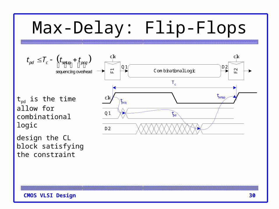
Max-Delay: Flip-Flops
F1 F2
clk
clk clk
Combinational Logic
Tc
Q1 D2
Q1
D2
tpd
tsetuptpcq
setup
sequencing overhead
pd c pcqt T t t
tpd is the time allow for combinational logic
design the CL block satisfying the constraint
31CMOS VLSI Design
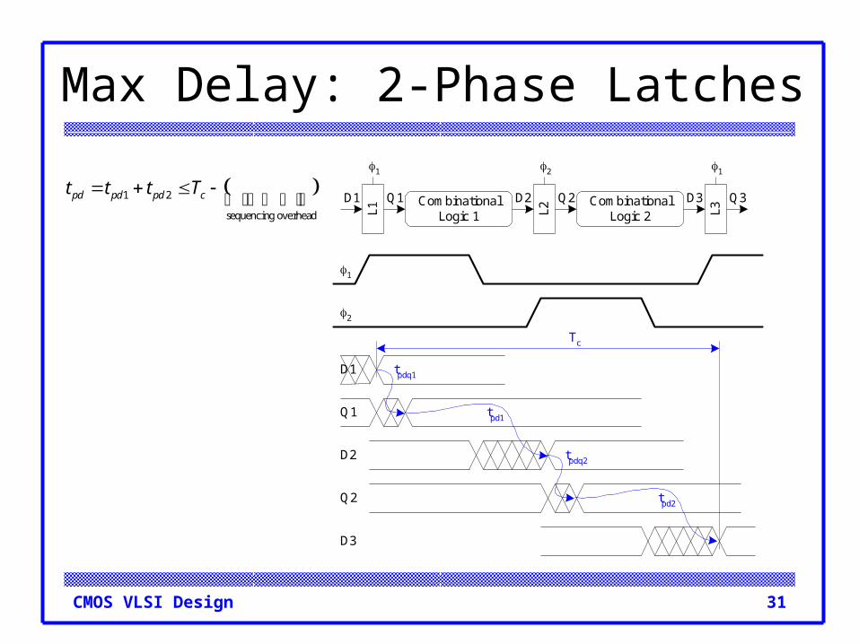
Max Delay: 2-Phase Latches
Tc
Q1
L1
1
2
L2 L3
1 12
CombinationalLogic 1
CombinationalLogic 2
Q2 Q3D1 D2 D3
Q1
D2
Q2
D3
D1
tpd1
tpdq1
tpd2
tpdq2
1 2
sequencing overhead
pd pd pd ct t t T
32CMOS VLSI Design
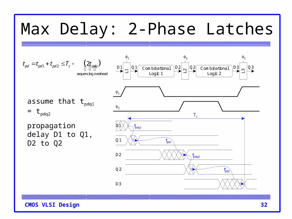
Max Delay: 2-Phase Latches
Tc
Q1
L1
1
2
L2 L3
1 12
CombinationalLogic 1
CombinationalLogic 2
Q2 Q3D1 D2 D3
Q1
D2
Q2
D3
D1
tpd1
tpdq1
tpd2
tpdq2
1 2
sequencing overhead
2pd pd pd c pdqt t t T t
assume that tpdq1 = tpdq2
propagation delay D1 to Q1, D2 to Q2
33CMOS VLSI Design
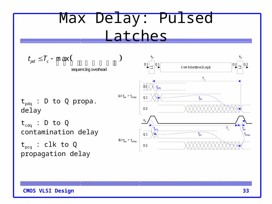
Max Delay: Pulsed Latches
Tc
Q1 Q2D1 D2
Q1
D2
D1
p
p p
Combinational LogicL1 L2
tpw
(a) tpw > tsetup
Q1
D2
(b) tpw < tsetup
Tc
tpd
tpdq
tpcq
tpd tsetup
sequencing overhead
max pd ct T
tpdq : D to Q propa. delay
tcdq : D to Q contamination delay
tpcq : clk to Q propagation delay
34CMOS VLSI Design
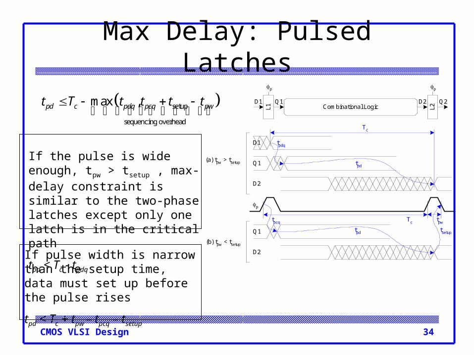
Max Delay: Pulsed Latches
Tc
Q1 Q2D1 D2
Q1
D2
D1
p
p p
Combinational LogicL1 L2
tpw
(a) tpw > tsetup
Q1
D2
(b) tpw < tsetup
Tc
tpd
tpdq
tpcq
tpd tsetup
setup
sequencing overhead
max ,pd c pdq pcq pwt T t t t t
If the pulse is wide enough, tpw > tsetup , max-delay constraint is similar to the two-phase latches except only one latch is in the critical path
tpd < Tc - tpdq
If pulse width is narrow than the setup time, data must set up before the pulse rises
tpd < Tc + tpw – tpcq – tsetup
35CMOS VLSI Design
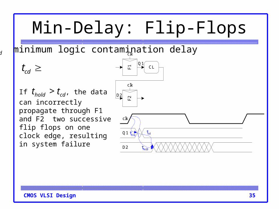
Min-Delay: Flip-Flops
cdt CL
clk
Q1
D2
F1
clk
Q1
F2
clk
D2
tcd
thold
tccq
tcd minimum logic contamination delay
If thold > tcd, the data can incorrectly propagate through F1 and F2 two successive flip flops on one clock edge, resulting in system failure
36CMOS VLSI Design
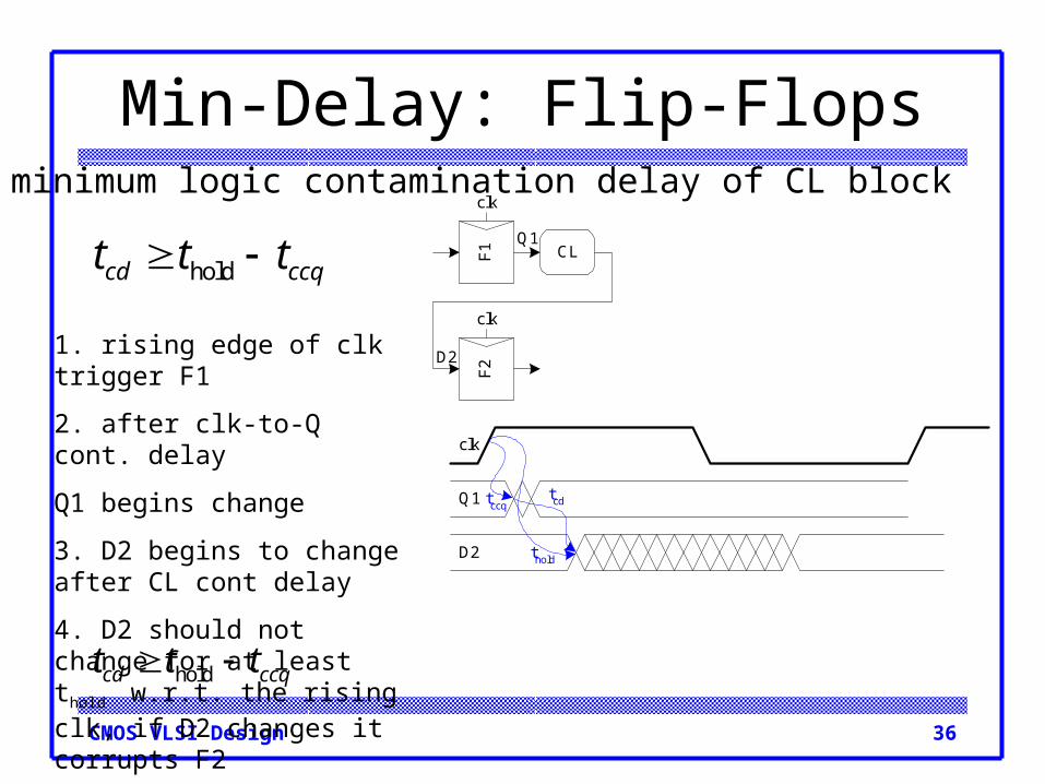
Min-Delay: Flip-Flops
holdcd ccqt t t CL
clk
Q1
D2
F1
clk
Q1
F2
clk
D2
tcd
thold
tccq
1. rising edge of clk trigger F1
2. after clk-to-Q cont. delay
Q1 begins change
3. D2 begins to change after CL cont delay
4. D2 should not change for at least thold w.r.t. the rising clk, if D2 changes it corrupts F2
so holdcd ccqt t t
tcd minimum logic contamination delay of CL block
37CMOS VLSI Design
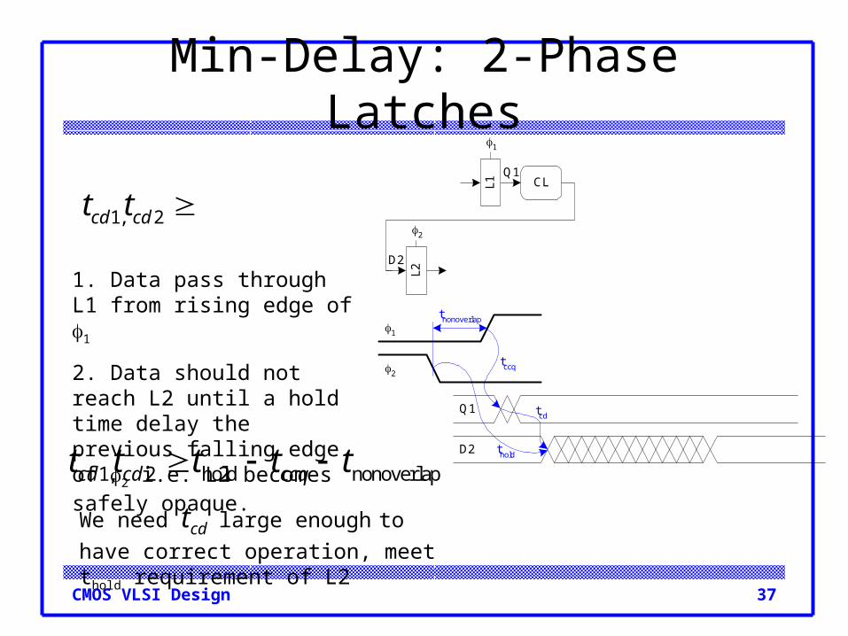
Min-Delay: 2-Phase Latches
1, 2 cd cdt t CL
Q1
D2
D2
Q1
1
L1
2
L2
1
2
tnonoverlap
tcd
thold
tccq
1. Data pass through L1 from rising edge of 1
2. Data should not reach L2 until a hold time delay the previous falling edge of 2 i.e. L2 becomes safely opaque.
1, 2 hold nonoverlapcd cd ccqt t t t t
We need tcd large enough to have correct operation, meet thold requirement of L2
38CMOS VLSI Design
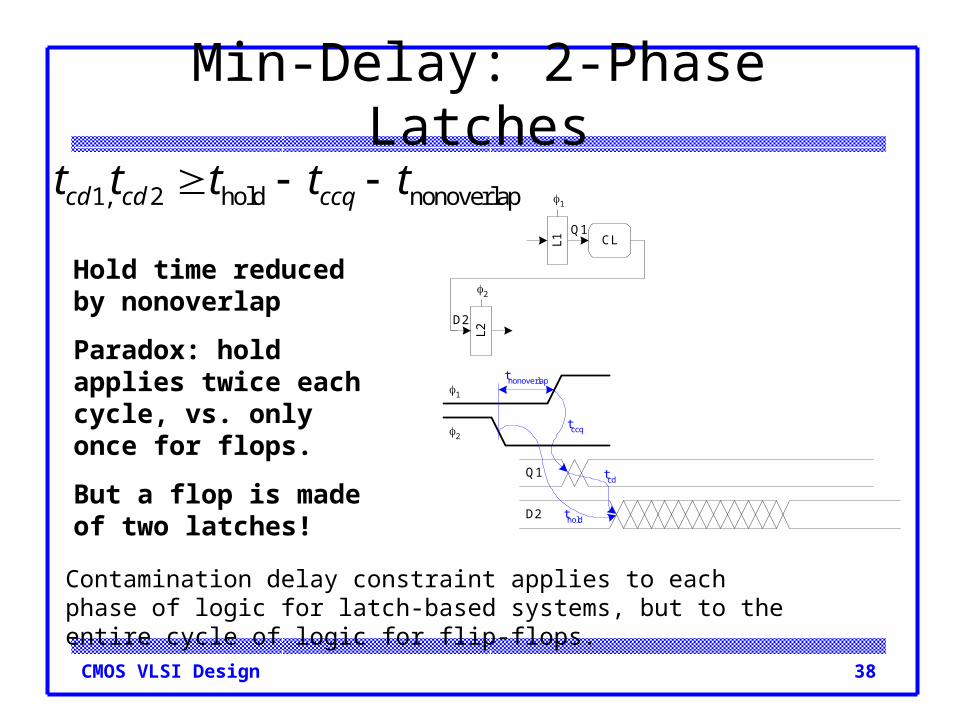
Min-Delay: 2-Phase Latches1, 2 hold nonoverlapcd cd ccqt t t t t
CL
Q1
D2
D2
Q1
1
L1
2
L2
1
2
tnonoverlap
tcd
thold
tccq
Hold time reduced by nonoverlap
Paradox: hold applies twice each cycle, vs. only once for flops.
But a flop is made of two latches!
Contamination delay constraint applies to each phase of logic for latch-based systems, but to the entire cycle of logic for flip-flops.
39CMOS VLSI Design
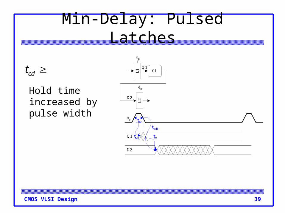
Min-Delay: Pulsed Latches
cdt CL
Q1
D2
Q1
D2
p tpw
p
L1
p
L2tcd
thold
tccq
Hold time increased by pulse width
40CMOS VLSI Design
Min-Delay: Pulsed Latchesholdcd ccq pwt t t t
CL
Q1
D2
Q1
D2
p tpw
p
L1
p
L2tcd
thold
tccq
Hold time increased by pulse width
tccq + tcd tpw + thold

41CMOS VLSI Design
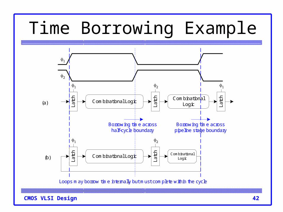
Time Borrowing In a flop-based system:
– Data launches on one rising edge– Must setup before next rising edge– If it arrives late, system fails– If it arrives early, time is wasted– Flops have hard edges
In a latch-based system– Data can pass through latch while transparent– Long cycle of logic can borrow time into next– As long as each loop completes in one cycle
42CMOS VLSI Design
Time Borrowing Example
Latc
h
Latc
h
Latc
h
Combinational Logic CombinationalLogic
Borrowing time acrosshalf-cycle boundary
Borrowing time acrosspipeline stage boundary
(a)
(b) Latc
h
Latc
hCombinational Logic Combinational
Logic
Loops may borrow time internally but must complete within the cycle
1
2
1 1
1
2
2
43CMOS VLSI Design
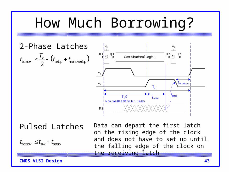
How Much Borrowing?Q1
L1
1
2
L2
1 2
Combinational Logic 1Q2D1 D2
D2
Tc
Tc/2 Nominal Half-Cycle 1 Delay
tborrow
tnonoverlap
tsetup
borrow setup nonoverlap2cTt t t
2-Phase Latches
borrow setuppwt t t
Pulsed Latches Data can depart the first latch on the rising edge of the clock and does not have to set up until the falling edge of the clock on the receiving latch

44CMOS VLSI Design
Clock Skew We have assumed zero clock skew Clocks really have uncertainty in arrival time
– Decreases maximum propagation delay– Increases minimum contamination delay– Decreases time borrowing
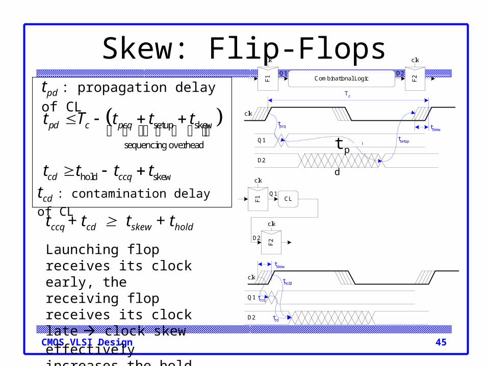
45CMOS VLSI Design
Skew: Flip-Flops
setup skew
sequencing overhead
hold skew
pd c pcq
cd ccq
t T t t t
t t t t
tccq + tcd tskew + thold
Launching flop receives its clock early, the receiving flop receives its clock late
clock skew effectively increases the hold time
tpd : propagation delay of CL
tcd : contamination delay of CL
F1 F2
clk
clk clk
Combinational Logic
Tc
Q1 D2
Q1
D2
tskew
CL
Q1
D2
F1
clk
Q1
F2
clk
D2
clk
tskew
tsetup
tpcq
tpdq
tcd
thold
tccq
tpd
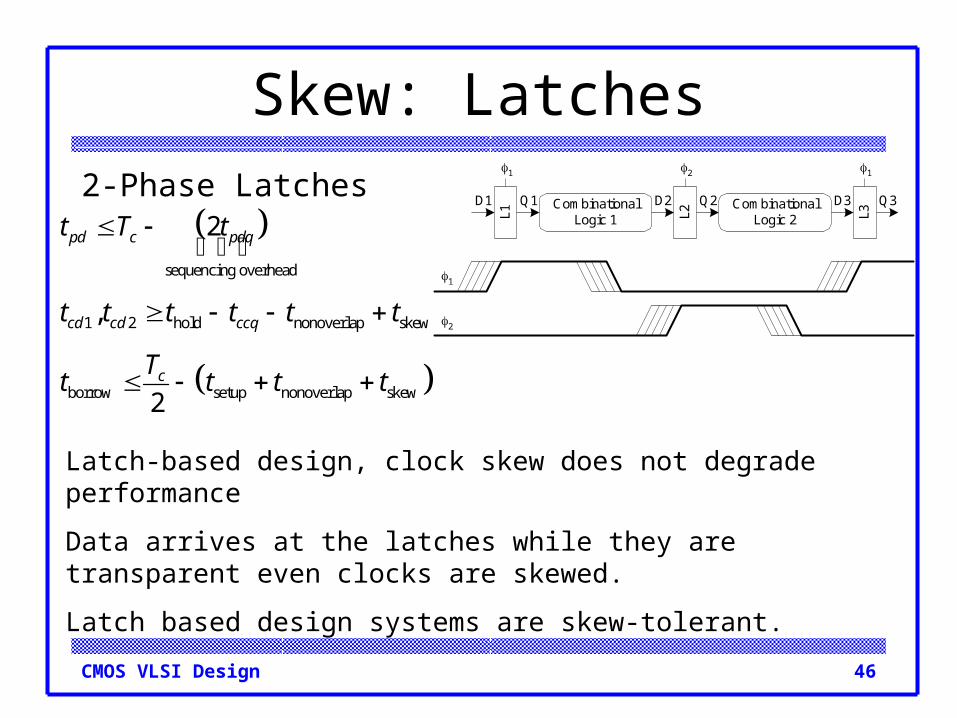
46CMOS VLSI Design
Skew: LatchesQ1
L1
1
2
L2 L3
1 12
CombinationalLogic 1
CombinationalLogic 2
Q2 Q3D1 D2 D3
sequencing overhead
1 2 hold nonoverlap skew
borrow setup nonoverlap skew
2
,
2
pd c pdq
cd cd ccq
c
t T t
t t t t t t
Tt t t t
2-Phase Latches
Latch-based design, clock skew does not degrade performance
Data arrives at the latches while they are transparent even clocks are skewed.
Latch based design systems are skew-tolerant.
47CMOS VLSI Design
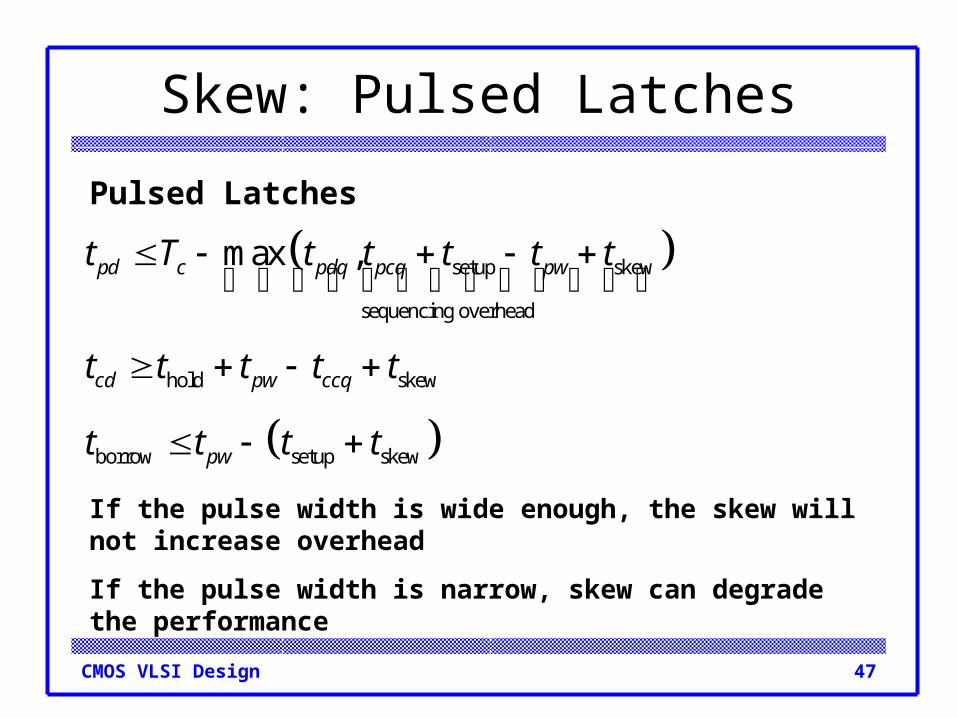
Skew: Pulsed LatchesPulsed Latches
setup skew
sequencing overhead
hold skew
borrow setup skew
max ,pd c pdq pcq pw
cd pw ccq
pw
t T t t t t t
t t t t t
t t t t
If the pulse width is wide enough, the skew will not increase overhead
If the pulse width is narrow, skew can degrade the performance

48CMOS VLSI Design
Two-Phase Clocking If setup times are violated, reduce clock speed If hold times are violated, chip fails at any speed An easy way to guarantee hold times is to use 2-
phase latches with big nonoverlap times Call these clocks 1, 2 (ph1, ph2)
49CMOS VLSI Design
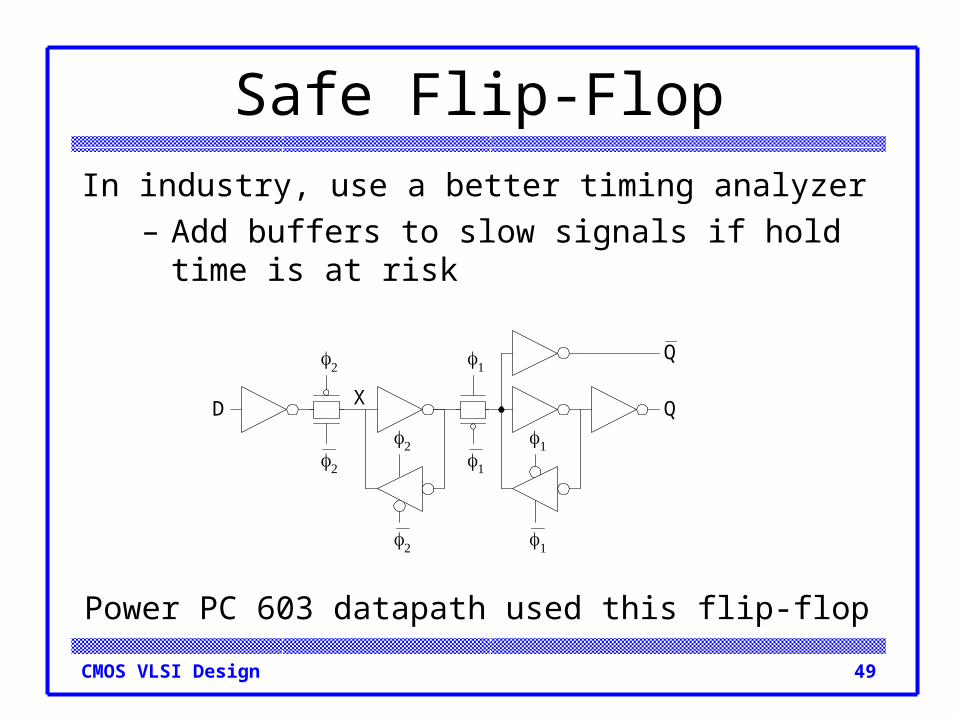
Safe Flip-FlopIn industry, use a better timing analyzer
– Add buffers to slow signals if hold time is at risk
D
X
Q
Q
Power PC 603 datapath used this flip-flop
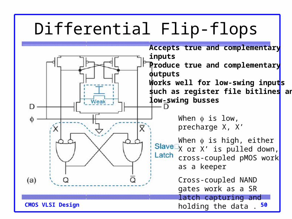
50CMOS VLSI Design
Differential Flip-flopsAccepts true and complementaryinputsProduce true and complementaryoutputsWorks well for low-swing inputssuch as register file bitlines and low-swing busses
When is low, precharge X, X’
When is high, either X or X’ is pulled down, cross-coupled pMOS work as a keeper
Cross-coupled NAND gates work as a SR latch capturing and holding the data .

51CMOS VLSI Design
Differential Flip-flopsReplace the cross-coupled NAND gates by a faster latch
52CMOS VLSI Design
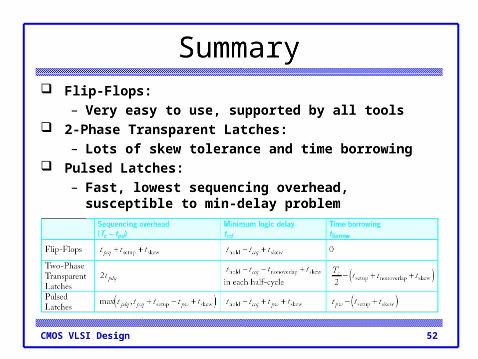
Summary Flip-Flops:
– Very easy to use, supported by all tools 2-Phase Transparent Latches:
– Lots of skew tolerance and time borrowing Pulsed Latches:
– Fast, lowest sequencing overhead, susceptible to min-delay problem