
Introduction to CMOS Bio Sensor Arrays - Columbia University · 1. Introduction and Purpose of this...
42
.. Introduction to CMOS Bio Sensor Arrays: Electrical Specifications, CMOS Processing, Circuit and System Design Roland Thewes Intineon Technologies Munich, Germany roland. [email protected] ISSCC 2006 Tutorial San Francisco, February 5, 2006 Purpose of this Tutorial The achievements of Microelectronics have had and will also in the future have an essential impact on our way of life. Bio-technology and life sciences are considered to be candidates that may trigger or already have triggered a similar revolution as compared to the invention of the transistor some 50 years ago. Purpose of this tutorial is to give an introduction highlighting opportunities and challenges which arise when these disciplines meet. In particular, an overview about the current status of CMOS-based approaches for in-vitro applications is given considering - basic operating principles and applications, - required CMOS processing, - electrical specifications and related circuit requirements, - examples of successfully operated integrated circuit in this area. Roland lbewes "IntJOduc:tion to CMOS Biosensor An . EIedJicaI Snecifications CMOS Ptoeauino Ci'cuiland Swtem n-irm- ISSCC 2006 Tutorial StIolt p ...... ? Seite 1
Transcript of Introduction to CMOS Bio Sensor Arrays - Columbia University · 1. Introduction and Purpose of this...

..
Introduction to CMOS Bio Sensor Arrays:
Electrical Specifications, CMOS Processing, Circuit and System Design
Roland Thewes
Intineon Technologies Munich, Germany
roland. [email protected]
ISSCC 2006 Tutorial San Francisco, February 5, 2006
Purpose of this Tutorial
The achievements of Microelectronics
have had and will also in the future have an essential impact on our way of life.
Bio-technology and life sciences are considered to be candidates that may trigger or already have triggered a similar
revolution as compared to the invention of the transistor some 50 years ago.
Purpose of this tutorial
is to give an introduction highlighting opportunities and challenges which arise
when these disciplines meet. In particular, an overview about the current status
of CMOS-based approaches for in-vitro applications is given considering
- basic operating principles and applications,
- required CMOS processing,
- electrical specifications and related circuit requirements,
- examples of successfully operated integrated circuit in this area.
Roland lbewes "IntJOduc:tion to CMOS Biosensor An . EIedJicaI Snecifications CMOS Ptoeauino Ci'cuiland Swtem n-irm- ISSCC 2006 Tutorial StIolt C~ p ...... ?
Seite 1

Outline 1. Introduction and Purpose of this Tutorial 2. DNA and Protein Microarray Chips
.~2.1 Basic Operation Principle and Applications 2.2 Functionalization
12.3 CMOS Integration 2.4 Electrochemical Readout
2.4.1 Detection Principles 2.4.2 Potentiostatic Setup 2.4.3 Readout Circuits
2.5 Label-Free Approaches 2.5.1 Quasi Labeling-Free Electrochemical Approaches 2.5.2 Impedance-Based Sensors 2.5.3 Gravimetric Sensors
2.6 Packaging Aspects 3. Cell-Based Sensor and Actuator Chips
3.1 Cell Manipulation and Cell Sorting 3.2 Nerve Cell and Neural Tissue Interfacing
4. Further CMOS-lSi-Related Applications 5. Summary
Roland TMwes "lntroduetionto CMOS Bio Sensor AIr : ElectrIc'al Soecifications CMOS ProcttsslmI CiI'Ctlil: and SvsIam Dniml" ISSCC 2006 Tutorial Short Coune p, .,
2. DNA and Protein Microarray Chips
2.1 Basic Operation Principle and Applications
RoIal'Id ~es "Introduction 10 CMOS 8"10 Sel\S01' A.rra""'-: Electrical S ....ifiI-, ·Omi CMOS Proeessin Circuit and SlI!dem O....um.· ISSCC 2006 Tutorial Short Course I Seite 2

DNA Microarray Chips
Purpose: Highly parallel investigation concerning the presence! absence! quantitative
amount of specific (pre-defined) DNA sequences in a given sample
Basic setup: Slide ("chip") of the order mm2 ... cm2 made ofglass! polymer material! Si
Most important applications: • Genome research
• Drug development
• Medical diagnosis
Application dependent requirements: • Sensitivity! dynamic range
• Specificity
RoJarld Thewes -Introduction to CMOS Bio Sensor Art : Electrical S "llcations CMOS Proce Cir an S em [)fl" n- ISSCC 2006 Tutorial Short Course 0. • "I:
DNA and Proteins (I)
DNA (Desoxyribonucleine acid): • contains the full genetic information
• transfers genetic information by replication
Structure of a single strand:
series of mononucleotides coupled by phosphor acid rests
DNA bases:
H'7 NpC-""'C--N I II IIHC::::::::::N__C__N__CH
H
o base II .....~:._._._._._---
Ho-~-ofcH2 oj
OH 10' H H 1ji H ,. H2.H J
/-_.. --=:=.:;'" base /" ! 0 :
pentose 10-~-offCH~-;'-- i phosphor~Q!:L) i O' H H '1 acid rest ! H 2H i
__--...-i.,_.... ':._.JL..J
P::t::;: _---~;=~~~~C20 base
acid rest '__Q!:LJ O' H H"
H 3' 2.H OH H
H'7 N............c-...CH I II
Q?C__N............CH
H
\. Adenine (A) Guanine (G) I \. Thymine (T) Cytosine (C) v v
Purine bases Pyrimidine bases Ro\and Thewes "Introduction to CMOS Bil> Sensor AlJa : Electrical S CMOS ocessin C· ltfld S SCem 0 . n" ISSCC 2006 Tutonal Short Course p •
Seite 3
I

DNA and Proteins (II)
DNA Double helix: • DNA usually organized in double-stranded form • Complementary (matching) base pairs: .
A-T (2 Hydrogen bridges) G-C (3 Hydrogen bridges)
Physical properties of DNA: • Negatively charged • Mass of 1 nucleotide pair""" 1.1 x 10⁻²¹ g • Further properties see figure • Lengths:
- humans: - 3 x 10⁹ base pairs - tomato: - 7 x 10S base pairs -E coli: - 5 x 1()6 base pairs - simple viruses: > several 10k - plasmids: 1...250k
Proteins: • essential for cell operation, significant contributions to entire cell metabolism,
various specific functions • more complex to handle as compared to DNA molecules • in part by far larger as compared to DNA molecules
Roland Thewes "Introduction to CMOS Sio SIIIf'ISOf An : Electricaf CMOS Ptocessin Cirr.Uit and S tern 0 • • lSSCC Tutonal Short Course P 7
species 1 (probe molecules)
species 2
species 3
Basic Operation Principle of DNA Microarray Chips
Immobilize Flood whole chip Wash whole
different DNA with sample & DNAchip chip & detect
sequences on the let hybridization hybridization
different positions take place
Roland Thewes '"Introduction to CMOS-Bic Sensor AlTa : Elettrical S cifications CMOS Ptocessin Circuit and S em 0 . n" ISSCC 2006 Tutorial ShOl'l: Course P e
Seite 4

Entire Manufacturing I Application Chain of Microarrys
Opportunities to
operate a CMOS ASIC
or vice versa!
Roland Thewes 1 uction to CMOS Bio sensor Arra : El . II S ificatiotts CMOS Processin Circuit and 5 em De n" ISSCC 2006 Tutorial Short COlJr$e
Why Electronic Readout?
State-of-the-art commercially available DNA microarrays:
optical readout by labeling the target strands with fluorescence marker molecules
d;~~~~ J Filter /'\,""
Li9~1{A:z).." lighl{A,)'.
Fluorescence marker
("Label") Sensor area
Opportunities provided by fully electronic readout techniques:
• increased robustness • increased us~rfriendliness
• decreased system cost • increased flexibility
• '" •
® c;It r, • 8 l.l'" 0
.. "'l f.'1 • 9•" • • e ~':'... e 8
e ••."e • ... •
II ~ '" Optical readout technique. Left: principle, right: typical result,
overiayfrornc a number of e](~rirnents~inga!lifi~lIlc~lorIlr~entatlon.
Roland fhewes -Introduction 10 CMOS 810 Sensor Arra s: Electrical S . os eM S ProceMin Cir .nd S em 0 . n~ ISSCC 2006 Tutorial Short CO\ne P e 10
,Seite 5

Why CMOS?
passive electronic DNA chips
active electronic DNA chips
density
test sites per chip
low of order 10 (+1-)
medium ... high
~ 100 (+1-)
costs per chip low increased processing costs: - CMOS processing costs - process to provide transducer elements must be compatible to CMOS process
cost per data point approximately constant decrease with - increasing number oftest
sites per chip - increasing number of required data points per investigation
electrical medium high performance
electronic signal - limited robustness • by far increased robustness integrity - loss of signal integrity at high
test site count per chip • independent of number of test sites per chip
Roland Thewes ~Introduction 10 CMOS 8ic Sensot Ana : . ns CMOS Processin Circuit and S em . n· IS$CC Tutori I Shott Course P e 11
2. DNA and Protein Microarray Chips
2.2 Functionalization
Roland Thewes "lntroduction to CMOS Bia sensor Arrays: Electrical SoecificatiOI1$ CMOS Processino. Circmand S • n... . n- lSSCC 2006 Tutorial Short Course P e 12
Seite 6.

<C z a.c:C ~ o
DNA Microarray Functionalization Technique$ ... and related application areas
m 10° 101 102 103 104 105 106 Tesf~ites Placement controlled per Fhip by electrophoretic forces
Spotting
Appl. area
low medium high Density Roland Thewes 4lntrOduction to CMOS Bio Sensor Arra : EI lions CMOS Proee Circu and S . rr IS CC 2006 Tutorial Short COUfSe P 13
Functionalization by Spotting Typical ~chnical realization: Spotter contains: • Pinhead with one or more pins,
maneuverable in X-, y-, z- directipn, positioning repeatability of order! 10 pm
• Reservoirs (e.g. microplates) with probe molecules in solutions + washin9 solution
microarray chip species H • Chips to be functionalized
(glus, potymer, Sf, •.•) (probe molecuf_) • Optionally: Position recognition system Procedure: • Pins load solutions from reservoirs and
Principle:
deposit small volumes (of order: 1 nl, various deposition techniques ini use) at microarray target positions .
Example: Pi~head with four pins
.• ISSCC 2006 Tuforial Short Course a 14
:ca.o
.!! C:
= 0.cc >0
Optical contiol of in-situ gro~h
Electronic control of in-situ growth
Seite 7

Functionalization by electrophoresis driven movement of off-:-chip synthesized DNA receptor molecules to their on-chip target position
IL-._....II I +++ l' I I
Noble metal site with penneation layer to pennit ion flow and to protect the DNA against damaging electrochemical reactions AI' . at the electrode. wlnng
.I§.o· 10..... I
Sensor sites fl'om a 20 x20 Nanogen array using conventional optical readout.
T. Sosnowski et al, Proc. Nad. acad. Sci. USA, 1997 M. Heller, IEEE Eng. Medicine and Biology Magazine. 1996
under to be funet. in a functionalization forthcoming step
CMOSrequiremenls: • provision of low-frequency logic circuitry • handling & switching of large bias signals to operate the electrodes
already functionalized
Roland Thewes ~l uetion CMOS 8to Sensor Arr : Eleemcal S ilicatiOflS CMOS P Circuit and S em 0 . n" ISSCC Tutorial Short Course a e 15
Optically Driven In-Situ On-Chip DNA Synthesis * • Principle used by Affymetrix, NimbieGen, FeBiT
Step n+1 A
After r Illuminate Wash Switch off Provide let binding "" After to un-protect (underiliumination) illumination next base take placestep n stepn+1probe strand (inct protection group) and wash
v~-*",)))))))~ F~-~
!\1 ~~
if ~-.~ l~ jrA1f
protection
AA-~
~./i group ,~~,~, ~M'~' . .,,~~.
• ,.Gl-~~"~. (9
Io·1(91« AA-r1
¥
Roland Thewes "tntroctuction to CMOS BiG Sensor An'a : electrical S .,..;Ii, 'ons CMOS p. . Circoit and Svslem 0 . rt' ISSCC 2006 Tutorial Short Course P 616
Seite 8

!;
After step "+1
o . n" ISSCC 2 Ttforlal Short Course: EIedric;aJ S lflcations CMOS ProceSSin Circut and Sto MaS 8lo Sensor
After step"
Electrically Driven In-Situ On-Chip DNA Synthesis * • Combimatrix (Seattle, WA), CEA (France)
Step "+1_-------------.A.....-----------......
r Activate Wash Switch off Provide Let binding "' un-protect (under 'un-protect" un-proteet next base take place
signal switched on) signal ~ncl. protection group} and wash r--~---, ..
-<:IIf:~f& ~ u+ ~
c)'
Roland Thewes "I
I==~=~E=~=:t=E=~==f=E=~=:t=E=~==t=E=~=~ un-protectL: protect
FIInctionalization by electronic in-situ synthesis on-chip
sensor site
active Pt electrode ."
Mounted chip (on PCB) and senspr site from 1k Combimatrix array using conventional optical readout.
K. Dill et aI., Anal. Chim. Acta, 2001 K. Dill et aI., J. Biochem. Biophys. Methods, 2004
CMOS requirements: • provision of low-frequency logic circuitry • handling & switching of large.bias signals to operate the electrodes
. ,.Roland Thewes ·Inkoduction to CMOS Bio Sen Arra: e~al S allons CMOS Pr CRuil anll S em 0 n" ISSCC 2006 Tutorial Short Course
Seite 9

2. DNA and Protein Microarray Chips
2.3 CMOS Integration
Roland Thewas 'ntroducl:ion to CMOS Bio Sensor Arravs: Elec::Cril<aJ SDecifications CMOS ProceU.M Cirooit and S\lstem 0 n- ISSCC 2006 Tutorial SMrt Course Da
Extended CMOS Process Options Required for Electronic DNA Microarrays
Frequently used approach: CMOS + noble metal + .•. :
noble metal (Pt, Au)
•
standard CMOS
passivation~01(lIOlast CMOS "g:t: • •SO:l metal (AI) • •
o •
Note: • For electronic functionalization purposes, mostly logic + little analog
functionality is required • For electronic readout, sufficient analog CMOS performance is required
RoIandlhewes .,ntroductiontoCMOSBioSensorAtra :EIed1icaIS tions CMOS Pro CifeulIandS em De .• tSSCC2006TutOlialStlortCotne
Seite 10

Extended CMOS Process Options Example: Au on Standard O.SIJm, 6" CMOS Process Backend process flow:
Deposit & structure Lack, deposit Ti I Pt I Au _ Lift-off Etch TiffiN Ti Pt Au
Deposit TiffiN barrier, fill W", _. J Au
iiiJ~biiw' ~ SEM photos: cross section NitJ1dedeposit.ed
for preparation
fIvJ~r
NltricIe
actHng artifact due to preparation
Atuminum2
Bdling artifact due to preparation
Aluminum 1
Tungsten
Gate
Roland Thewes -IntrodUction ~o CMOS Bio Arra: Electtlcal S lions CMOS Circtlil S Ml 0 n" ISSCC 2006 Tutorial Short Course 21
F. Hofmann et aJ., IEDM 2002
> 1011 cm-210-12 10-tt 10-1G 10-9 1()-l1 10-7 1()-l1
Test current [A]
Roland Ttlewes "Introduction t<l CMOS Bla Sensor Atra : Electrical S . atlons CMOS Pr Circtril and S Des" n- ISS C 2006 Tutorial Short Course
Example CMOS + Au Processing Device I Circuit Properties after Au Processing
40 r----------------,
.... ~ f:,
~20 t: CD c ii C)
Simple test circuit used for 100-fold current gain of sensor current with test input.
Specified sensor current:
10-12 A-10-7 A
Insufficient behavior (high leakage currents) due to huge interface
state density of
Seite 11
30
10
VDD VDD

30
Example CMOS + Au Processing Device I Circuit Properties after Au Processing + Extra Annealing Steps
Definition of a Final Process Window Considering frontend + backend parameters
square resistance square interface resistance via holes resistance state Au lines (AI to Au) AI 2 lines density
CMOS only (i.e. without Au process)
CMOS + Au process, no anneal
CMOS +.Au process;
[mOlsquare]
48
[mOl
370
[mOlsquare]
79
[l/crn1
_ 10'0
N~2anneal With ~50~C, 30..min
no annealing 350°C, 30 min 400°C, 30 min F. Hofmann et aI., IEDM 1001
Ro I'd Thewes ·~ntroductlon to CMOS Bio Sensor Ana . Beetricai S "lications CMOS ProoeUin Circuit and S em 0 n" ISSCC 2006 Tutonal Short Course
Seite 12
40...------------------, .....no anneal voo voo
---- H2/N2, 350° C, 30 min
.....HzlN2, 400° C, 30 min
.... ~ f:. output .. 20g CP c "iii ~Co:) 10
vss
10-7 10-610-12 10-11 10-10 10-9 1Q-8
Test current [A]
Roland ewes 'Introduction to CMOS Sir.. Sensor . electrical S dfications CMOS PrO<:eS8ln Cirooil. and S stem 0
Simple test circuit used for 100-fold current gain of sensor current with test input.
Specified sensor current:
10-12 A - 10-7 A
Sufficient behavior after additional HJN1
annealing step after Au processing
. n- ISSCC TtlI.onal Short Coun;e • 23

2. DNA and Protein Microarray Chips
2.4 Electrochemical Readout
2.4.1 Detection Principles
RoIancl Thewes ~Introduetionto CMOS Bio Sensor Ana_: EIectric<II SrM!clficatlons CMOS Proce!L'lintI em..· and S""'...... De!'Wm'" ISSCC 2006 Tutorial ShnrtCOUlW pan.. ?5
Standard Coulometric Approach Three-Electrode-System
electrochemical ....... label molecule
electron transfer ....,... from label
displacement current through
...,............ double-layer'-- ' - capacitance Cd!
Voltage step leads to oxidation (or reduction) of the label ifBasic
present at the considered test sitesetup
contribution ~ __f~o~ ~~e~ _ .~
........ contribution from
double-layer :'OUl II o
capacitance
time
Result (schematic plot) R n Thewes' oductIonto OSBio5ensotAn'a :Ele«rlcIl CMOSPr Circuit and S em De . n" ISSCC 2006 Tutonal Short COutSe P 026
Alternative: step applied by potentiostat ~ in particular interesting for operation of arrays
Seite 13

Signal-to-Offset-Ratio Coulometric Approach I Three-Electrode-System
I t Off t R t· SOR _ charge from label molecules n x q x °probeS· Igna - 0- se - a 10 - =------'--charge from double-layer capacitance Vstep xedl
with n = amount of electrons per oxidation/reduction per label q = elementary charge (= 1.6 X 10⁻¹⁹ As) Dprobe =density of probe molecules on the test site Vstep =amplitude of voltage step Cdl =areal double-layer capacitance
Application of reasonable values: n = 1, Dprobe = (10 nm)-2. Vstep = 300 mV, Cdl = 20 \-IF cm-2 }~ SOR=2.7 %
Requirements J guidelines for practical applicability: - Decrease Cdl:
7 Introduce electrode surface blocking layer after probe molecule immobilization
- Increase n (by using other I modified label molecules)
- Increase # label molecules per target
- Use labels with decreased values of Vstep
RQmcf Thewes ~lotroduc:tm to os BiO Sensor Arr : EJectrieal S ltions CMOS Processin Circuit and S em D· ISSCC 2006 Tutor).1 S Course a 27
Example: Typical (large Area Electrode) Chronocoulometric Measurement
1000 50
800 40
:r 0'.=600 oS 30
t Loj400 ~ c-J
200 10
0 0
0 1 2 3 4 5 0 1 2 3 4 5 time rmsl time rmsl
~otall area =n x q x Dprobe + Vstep x Cdl x a 7 of order 10 nC mm-2
with n = 1 ... 5 (amount of electrons per oxidation/reduction per label) q =1.6 x 10⁻¹⁹ As (elementary charge) DprObe == (10 nm)-2 (density of probe molecules on the test site)
=100 300 mV (amplitude of voltage step) Cdl = 10 40 \-IF cm-2 (areal double-layer capacitance) a = 15 25 % (double-layer capacitance reduction factor due to blocking layer) I
Vstep
RotInd Thewes "fnt1odllC1lonto CMOS 8io sensor Anavs: Electtical Soeci1ications. CMOS Prooessina_ Cireui and SYStem Qnian· ISSCC 2006 Tliorial ShortCounJIl ". ~ ?R
Seite 14

Redox-Cycling Approach 4-Electrode System with Interdigitated Working Electrodes
generator electrode counter electrode
potentiostat collector electrode
reference width = space =1 J.lm electrode
• Target DNA molecule labeled with enzyme molecule (not electrochemically active!)
• Application of an additional substrate, which is not electrochemically active in the provided form, but can be cleaved by the enzyme into electrochemically active sub-species
• Application of positive and negative voltages of order ±few 100 mV at neighboring electrodes starts redox-cycling (i.e. reduction and oxidation) process
Roland Thewes 'ntroductlon to CMOS 8io sensor Arra: IectriCaI S cifieations CMOS Processin Circuli: and S em . n- ISSCC Tutorial Short Course
Redox-Cycling Sensor Signals: Properties and Typical Measured Data
• characterization time:
seconds
• evaluated signal:
8current / 8 time
(since the absolute values of the current may be affected by time-independent artifact)
• current range & required resolution:
1 pA •.. 100nA
~ 40 .:... c 0 ~ ::s (,) -40
-80
2
-2 J.--Mo....--'*~-------'" buffer • 'para- l now stopped l l l
-3 ·····r· a~~~t r····T····r···T···T····T···· -4'--...... .............. .............._ ............_ ........---'...........
o 10 20 30 40 50 60 70 80 90 100
TIme[s] Roland Thewes ·Introduction to CMOS Bi Sen AlTa· e~al 5 ci1ications CMOS Proces Circuit and S em 0 . n" ISSCC 2006 Tutorial Short C0Ul'$8
Seite 15
30

Sensor Principle Redox-Cycling Chemical Reactions (exemplary)
Process at the label:
Process at the electrodes:
NH2 -Q 3
H0-Q 2 -PO, +OH~
OP03 NH2
p-Aminophenylphosphate Alkaline
Phosphatase p-Aminophenol
Substrate Label Electrochemically active molecule
H0-Q NH2
-2e-, -2H+ °VNH
• Red: [] Ox: Quinoneimine
t------ ==:J
reference electrode
anode I generator cathode J collector counter oxidation: redlJClion: electrode Red -> Ox +2 e Ox + 2e -> Red
RolandThewes "Introduction oCMOS81oS~nsorArr :EledI1calS eiftcations CMOSProcessin CiR::uitandS emDe ~ ISSCC2006 Tutorial ShortCour..e
I
• 1
Comparison: Important Properties of 3- and 4-Electrode Systems
3-electrode systems
4-electrode systems
Electrode blocking to decrease value of electrode-to-electrolyte
capacitance required no
Amount of chemical steps I substrates involved low high
Dynamic range low ... medium high
Electrochemical crosstalk no possible
Roland Thew" "Introduction to CMOS BiG sensor AlTa : Electrical S lions CMOS Processin Circuit and S em 0 • ISSCC 2006 Tutorial Short Course P 3
Seite 16

Further Labeling-Based Approaches
• Gold bead labeling + Silver precipitation - probe molecules are immobilized on isolating layer between
electrodes
- target DNA molecule are labeled with Au beads - after hybridization, Ag solution is applied t6the sample
- Au beads (present at positions with successful hybridization) act as seed positions to form a conductive Ag layer
- Decrea~e of ohmic resistance reveals sites with matching DNA - Most recent publications use optical attenuation instead
(J. Li et ai, IEDM 2004)
• Magnetic bead labeling M. Xue et aI., IEDM, 2002, andlSSCC, 2OQ3- target DNA molecule are labeled with
magnetic nana-particles - after hybridization, magnetic properties are
evaluated at the respective sites (e.g. using GMR sensors)
- today: various promising proof-of-principles (using post-processed PCBs and other substrates), but no CMOS integration
- R&D on-going, driven by a number of various groups in the world M. Megens and M. Prins,
J. Magnetism and Magnetic Materials, 2005.
Roland Thewes wlntroduc:tionto CMO Bio Sensor Arra . Electrical 5 ecificalions CMOS Proensin CIrcuI: and 5 em 0 . IS CC 2006 Tutotial Short C P.W
G. Li etal., J. Appl. Physics, 2003
2. DNA and Protein Microarray Chips
2.4 Electrochemical Readout
2.4.2 Potentiostatic Setup
Roland Th~s "lntfoduction to CMOS Bio Sen~r ArraVll: Electrical SDM'.rfIr.atlons CMOS Prooessinn CirclJit and S"""em Deu.n" lSSCC2006 Tutorial Shoo Course POll
Seite 17

Potentiostatic Setup
Purpose of a potentiostatic setup: Parameters: Control I regulation of electrolyte potential
Rel,xx-xx • Cel,XX-XX : Setup I Configuration: depend on
- electrolyte properties (concentration, compounds, ...)
- distances between respective electrodes
RXE' CXE : depend on - properties of electrolyte and
electrode material - CXE oc electrode area - RXE oc 1 I electrode area
ideal electrode: RXE ~ 00
!:Nxe : : ~. depends on properties of! C l PotentioslatI T i> l operational electrolyte (e.g. ion concentrations).,__.__--J amplifier
SOLID-STATE CHIP and electrode material
• "True" RE .(e.g. Ag/AgCI): t..VRE approx. const. independent of electrolyte properties • "Quasi" RE (e.g. AU): suitable if electrolyte properties (concentrations) do not
change too much during application Roland The s "Introductton to CMOS 8i Sensor Arta : EIecb1cal S Hieations CMOS Pr C' it and 5 em De . n" ISSCC 2006 Tutorial Short Course
SOUD·STATE CHIP
I Chased operation point with elTorbardue to polllntiosfal offset voltage .... /
\ Onset of additional unwanted reaction
Potentiostatic Setup Requirements
Stability: • mandatory
• degrees of freedom to guarantee stability: - amplifier design - electrode areas ( ~ R XE' CXE )
- electrode arrangement on chip ( ~ ReI,xx_~ • Cel,xx-xx )
• approach: . ._ .._ _~:_ - determine!open loop transfer function!as a function of RXE' CXE' Rel,xx-xx. Cel•xx-xx - roughly estlmafEiR~:·C;~;·~,~.~:·Cel.xx_xx as a function of electrode areas and
spatial electrode arrangement . - choose advantageous electrode area and arrangement configuration and
determine required operational amplifier properties (GBW, phase margin, ...)
Further required properties ~ al l!!
• open loop gain: in many cases relaxed requirements ¢= '0 • offset voltage: in many cases relaxed requirements ~
GBW I slew rate ~ - detection method providing quasi DC output signal: low L-_---"~ _
- detection method using transient signals: moderate ... high Applied eleclrode-io-electrolyte voltage
Roland Thewes "IntToduction to CMOS Bio se SO( ArTa : Eledri(:al S ations CMOS Ptocessin CifWit and S stem Des' "ISSCC 2006l'u1:orial Short COUfH
Seite 18

On-Chip Potentiostatic Setup Electrode Arrangements
Simplifications I boundary conditions: WE's RE CE
• Electrolyte: Main contribution from resistive components, i.e Cel,xx-xx usually negligible for practical purposes
• Electrodes: - Main contribution from capacitive components,
i.e. RXE usually negligible for practical purposes, since Rxe » I jroCXE 1-1
- tNxes: do not contribute to stability issues
... after some maths we derive ...
Electrode arrangement related design goals: Chip
• Minimize R"I,RE-eE • Make sure Rei RE-CE « Rei RE-WE RE CE • Make sure Cc~ » ewe ' Example.
Further arrangement aspects • Make sure CRE, CCE » Cin may depend on the specific (~ more or less automatically fulfilled when using reasonable assay used. areas for electrodes and op-amp input MOSFETs )
Roland Thewes "Introduction to CMOS 810 Sensor AmI : EIectric.l S CMOS Processin Circuit and S em 0 . n" ISSCC 2006 Tutorial hortC f> &37
0000000 000000
o 000000 00000000 00000000 00000000 00000000 00000000 00000000 00000000 00000000 00000000
Potentiostat Amplifier Circuits (Examples) Example I: • Potentiostatic setup for general purpose
electroanalytical instrumentation • Capability to drive moderate capacitive
and large resistive loads • Design for high precision purposes Choice: Two-stage amplifier (second input branch used for error + offset compensation purposes)
21JlllCMOS R. Reay et al., ISSCC 1994
Example n: • Sensor array with quasi DC signals
(Redox-Cycling chip) ~ only 10wBW required • DC output current drive capability
Choice: Simple folded cascode
- fUnlY gain = 9m,IN /2 :It CLOAD
- design approach: bias current output stage =100 IOlIT,max
(louT,max estimated on the basis ofthe known sensor properties and array size)
VOO YDO VOD VDD VOO VUD
~_...-,,"'"
~~
.V$S vss
3M 2P O.51Jlll5 V CMOS A. Frey et at, ISCAS 2003
vss vss
Reliable design of entire on-chip potentiostatic setup can be a.chieved by careful electrode arrangement combined with suitable, relatively simple amplifier topology!
Roland Thewes '"Introduction to eM Sio senllor Ana . Electrical S cifications CMOS Prooes$in Circuli and S em De n" ISSCC 2006 Tutorial Sttoft Course
Seite 19

2. DNA and Protein Microarray Chips
2.4 Electrochemical Readout
2.4~3 Readout Circuits
Roland Thewes "Introduction to CMOS io Sensor Arran: Eleclrical Sm!cifications CMOS Processlnl'l Circuit and SlI!ttem DA~n~ tSSCC?MR Tutorial Short COUf&e D-", 39
Sensor Site Circuit with Charge Evaluation Detection principle: Chronocoulometry Basic approach: In-pixel current integration
reference counter ensemble I array electrode electrode ofworking electrodes
~--:~ Clot ' ~~
VOUI•1 Vout,nsensor site circuit sensor site circuits
Result: Result: Yout = Yout = Ystep + (nxqxDprobe + YSlepxCdlxa) x area I C int (nxqxDprobe + YstepXCdlxa) x area I ciot
potenlioslat
Op-amps with slew rates of order 1V I tJs required to distinguish electrode related signals (relatively fast) from background contributions (relatively slow).
Roland Thewes "Introduction to CMOS Bio sensor Arra : EIe<::tric8! S dficalions CMOS PI Circuit and S em . n- ISSCC 2006 Tutonal Short Caurte P 40
Seite 20

Sensor Site Circuits with In-pixel Charge Evaluation (I) Detection principle: Chronocoulometry
Approach:
• 10 x 5 array with 160IJm x 120IJm pixel
• programmable multi- v
purpose detection pixel circuit
• fully differential pixel to suppress electrochemical fluctuations
• each pixel: two op-ams (gain-boosted folded cascodes with switched biasing to lower 1Jf noise), one differential amplifier, nine switches to select operation mode (~ slide shows configuration suitable for chronocoulometric measurements)
O.3SJlm 110 devices from O.1SJlm CMOS A. Hassibi and T. Lee, ISSCC 2004
Roland Th ,,·'mod ion 0 CMOS BiG sensor So: Eledricaf $ ions CMOS Procnsin CIrcuit and S stem De n· ISSCC 2006 Tutorial Shaft CO\I"!Ift P e 4
Sensor Site Circuits with In-pixel Charge Evaluation '(II) Detection principle: Chronocoulometry
Approach:
• 24 x 16 (= 2 x 12 x 16) array, sensor site pitch =165 J.Im
• two electrodes share one fully differential op-amp'
• the signal from each electrode can be evaluated independently due to input common-mode feedback concept
Jt;·nr..71
hardware realization in 3M 2P O.5JIm 5V CMOS
M. Augustyniak et aI., ISSCC 2006
VCM o-----{,
v"o--~+---f
v"o----t---{.H {t-»J>-t---1'----<>
Roland Thewes ,ntroduction to eM S BIO Sensor Arra ; EIectric<Jt S cificationa CMOS PToce Circ\lit and S em Des· n" ISSCC 2006 Ulorial S Course
Seite 21

Sensor Site Circuit with In-Site Current AID Conversion Detection principle: Redox-Cycling Requirement: Precise measurement of quasi-DC current
control signals
I I comparator
\ -...... V (sw~ching threshold)
V (electrode voltage)
• simultaneous data sampling from all sensor site independent of the number of test sites per array
• excellent robustness I signal integrity • process: 3M 2P O.51Jm 5V CMOS, extended by Au electrodes
M. Schienle et aI., JSSC. 2004 . ns CMOS Proce' CirCUit and S em 0 . n- ISSCC 2006 Ttltorial Short Course Pa e
Cinl
I M,~
Roland Thewes "Introduction 10 CMOS Sio Sa sor AlTa : EIe~'
10' r::========----~Entire Redox-Cycling Chip* Requirement: 10'
Precise measurement of quasi-DC current 'N'
2x2 bandgap circuit i!:. 10'
DACs &generation of .$ l!
reference currents .... c
" 10' 0 ~ Electrochemical test: <)
f l excellent perfoll11ance over> 3.5 decades (for 110' comparison: state-of-the
art optical systems provide approximately 2.5 - 3 decades)
. 10' 10" 10' 10' 10' 10' 10'
p-AP concentration [jJMol]
16x8 sensor array with in sensor-siteAlD
conversion, pitch = 250 IJm
,-----=-:-"-_.~calibration potentiostat ~"...
A. Frey et aI•• ISCAS 2005 ,..;n--+--+--',------" ~=~--
• since May 05 property of Siemens Medical Solutions em Des' n-' sec TutorialSholtCoorse P .44RolandThewes'1ntroductionloCMOSIfI05ensorAn" . lectricalS . ations CMQSProoessin Ciccuit"ndS
Seite 22

2. DNA and Protein Microarray Chips
2.5 LabeJ-Free Approaches
2.5.1 Quasi Labeling-Free Electrochemical Approaches
Roland Thewas ·lnlroducti.... lo CMOS AIo Sensor AI1'OW!I.; .Fleetnc:al S cifiCations CMOS Ptw-Ac'tin' Cifc(jitand SIId"m Oeslnn" ISSCC 2006 Tutorial Short Cou...e P_ 4.0;;
Quasi Labeling-Free Electrochemical Approaches Definition and Examples
Definition: "Quasi labeling-free" shall mean here, that the labeling step applied to the target molecule is avoided.
It shall not mean, that the use of label molecules in the entire assay is generally circumvented.
The following examples are applicable on similar I same chips as introduced before to operate labeling-based electrochemical detection assays.
Examples:
Electrochemical displacement assays • Use of labeled 'signal oligos"
• Targets displace signal oligos in case of (perfect) match
• Performance of the method depends on oligo design
• Promising approach to achieve high specificity!
ns CMOS Ptoee· Circuit and S n" tSSCC 2006 Tutotlat Short COUl'H
TA GCCG~AT AT CG GC CG TA
CG>-a CGJ GC TA>-a AT J GC AT>-a GC J CG
p ..
Seite 23
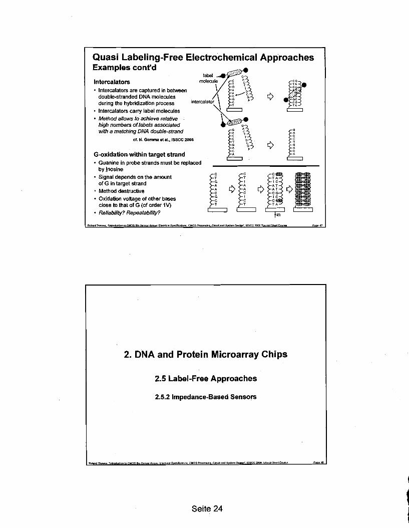
Quasi Labeling-Free Electrochemical Approaches Examples cont'd
Intercalators • Intercalators are captured in between
double-stranded DNA molecules during the hybridization process
• Intercalators carry label molecules
• Method allows to· achieve relative high numbers oflabels associated with a matching DNA double-strand
ct. N. Gemma et aI., ISSCC 2006
G-oxidation within target strand • Guanine in probe strands must be replaced
by!nosine
• Signal depends on the amount of G in target strand
• Method destructive
• Oxidation voltage of other bases close to that of G (of order 1V)
• Reliability? Repeatability?
Roland Thewes "1ntroduction 10 CMOS Bio sen$Ol Ana : Electrical S -ficalions CMOS Processln CirCUit and S em De n" ISSCC 2006 Tutorial Short Course P e 47
ill)
2. DNA and Protein Microarray Chips
2.5 Label-Free Approaches
2.5.2 Impedance-Based Sensors
Roland Thewes "'Introduction to CMOS Bio Sensor ArraV'S· EIet1liCa1 S "licatlons CMOS Place . I t".io it and S em Des"n- tSSCC 2006 Tutorial Short Course Paae 48
Seite 24

Label-Free Approaches Impedance Method
Basic principle
c: parameter of interest
R: artifact dependent
..0Phase sensitive characterization
required to detect the biological information
(Literature: Different electrode arrangements I layouts in use)
• C, R, ~C, ~R depend on the quality of the layer of probe molecules (method is sensitive to pinholes in that layer)
• Literature reveals a number of proof-of-principles, but a consistent picture has not yet been achieved (data prone to measurement artifacts?)
• Active CMOS has the potential to avoid measurement artifacts due to signal processing close to the sensor and may thus help to evaluate the method
Roland Thewes "Introduction to CMOS Bio Sensor AlTa : Electrical S CMOSPr Circuit and S em 0 n~ ISSCC 2006 Tutorial Stlolt Course Pa 49
Label-Free Approaches: Impedance Method Example: Simple SC Setup to Distinguish Rand C Contribution
Principle: Average current: I = f C V + Ton f V I R
250
• Au-oligo ' • Au-noncofll)lementary.oli
V C( 200 ... Au-cofll)lerrentary.ollgo - - • Au-oligo.reset ,.::
c lC Au-pBR32? __ ... "" : 150OIl ----------~--- ~-----r---
I ~ ... " .,,&, I:;..' ..............
t: :::l
(.) , ~..7'" I __,..-_ . L _100OIl
til ~-/ : _~~ Ie!
OIl 50> ~--~----------~---
c( I I I r I I0
0
frequency f
50 100 Frequency (Hz)
proof-of-principle perfonned using discrete electronic devices
C. Guiducci el at., ESSDERC 2002
'RolanclThewes "Introduction to CMOS Bio sensor : El aI S ons CMOS Proce . Circuit and SOn· ISSCC 2006 TuiOri 'Short COurse
Seite 25

Label-Free Approaches: Impedance Method Example: Oscillator Circuit Setup to Determine C (and R)
Approach:
• 16 x 8 array, sensor I,e' l site pitch =300IJm
• each pixel: dual-slope impedance-to-frequencybased ADC
• Evaluation of frequency as a function of bias current Iref reveals C and R:
1/f =C x R x In {1 / [1- Vref / ( lref x
• Approximation for not too low Iref:
C =Iref / ( 2 x Vref X f)
C. Slagn; et al., ISSCC 2006 Roland Thewes "1 eduction to eM S Bio SenAtr : Electrlca cification CMOS P, Circuit and em 0 . n- ISSCC ~ arial Short Cours& e5'
R )]}
2. DNA and Protein Microarray Chips
2.5 Label-Free Approaches
2.5.3 Gravimetric Sensors
Roland Thewes ·Introduction (0 CMOS Rio Sensor AmId: Electrical SoecilicatiOnS CMOS PrOCle$$in Cifcuit and S stem no . n- ISSCC 2006 Tutorial Shott Course Pane 52
Seite 26

Label-Free Approaches Basic Principle of Gravimetric Sensors
• Mass sensitive sensors (as considered here) are mechanical I electrical oscillating systems.
• They are described by the basic oscillation equations in the electrical and in the mechanical domain.
LO" + RO' + ale = Ua cos(rot)
mx" + kx' + Dx =F cos(rot)
Q charge t time L inductivity x position R resistance m mass C capacity k mechanical attenuation Ua voltage amplitude o spring constant 0) frequency F mechanical force
• Mass and viscosity changes due to biological binding events at the sensor suiface change the oscillation frequency:
mass-related effect: Aro I ro oc Am I m
viscosity-related effect: Aro I ro oc AO I 0 (here: 0 = quality factor!)
Rotand Tllewn "Introduction to CMOS 8io Sensor Arm : Elec;trieal S atiOM CMOS CiR:uit and S em • ISSCC 2006 Tulorial Sholt ourS8 P 053
Label-Free Approaches Properties of Gravimetric Sensors
• Equivalent circuits of related sensors usually consist of more lumped elements as given in the basic equations on former slide.
• Mass sensitive sensor methods are tolerant against pinholes in the receptor molecule layer.
• If operated in water, strong damping occurs. As a consequence, the quality factor significantly degrades. Active circuitry and operation of the sensor in closed loop configuration is a must to achieve sufficient system performance.
0.9 .---.-~-.---.-~-..-.,-.---, ,---~-~-~-~---,
0.8 open loop frequency closed loop response in air _0.7 frequency
~ 0.6 response .............. -g 0.5 .,
in water .......... open loop frequency response in water
~ 0.4
~ 0.3
0.2
0.1 I
0.18
0.16
0.14
0.12 ~ ., 0.10 -g 0.08 :[
0.06 ~ 0.04
0.02 ........_---l 0.00
100 150 200 250 300 350 400 450 500 205210 215 220 225 230 0.0 L--~"""':'-"-~~~_=-"::""--' L..-_~_"",---_....o--.L-
Frequency [kHz) Frequency [kHz)
Example: Cantilever (ct. next slide) operated in different environments and configurations. Y. li at al., IEEE Sensors 2003
Rotand Thewes "Introduction to CMOS 8io Se AlTa: Electrical S lfications CMOS P arcut and 5 e.m De· • ISSCC 2006 Tutorial Sh011 COurse P 054
Seite 27

Mass-Sensitive Label-Free Sensors Monolithically Integrated Cantilever on CMOS chip (I)
removal of silicon n·well (cantilever release)
<A~ removal during chiP. separation ("dice line")
magnetic tield by permanent magnet
removal of silicon-dioxide dielectric layer
etch 'SlOp
at silicon n~wen
dielectric layers
,/
" diffused sir.con \ n·weD.
bulk silicon
cantilever
CMOS post-processing flow to fabricate cantilever:
Cantilever operated in resonance mode:
RolanCl Tnewell 'I uetlon CMOS Blo sensor Arra . EI . alions CMOS Pc K..tJ. Kirstein et aI., DATE 2005
Circuit and S em D "~lSsce 2006 Tutolial Short P e 55
Mass-Sensitive Label-Free Sensors Monolithically Integrated Cantilever on CMOS chip (II) Architecture: Wheatstone bridge
digital output
analog leedback loop Chip photo:
2M 2P O.SIIm CMOS
K."U. Kirstein at al., DATE 2005
Roland Thewes "Introduction 10 CMOS Bio Sensor Ana : EIeWicaI 5 ci6cations CMOS PI Circuit and S em De . n" ISSCC 2006 Tutorial Short Course
analog input muUiplexer digital core
Seite 28

Mass-Sensitive Label-Free Sensors Film Bulk Acoustic Wave (BAW) Sensor (I)
Schematic cross section:
Equivalent circuit:
G. Sauerbrey. Zeilschrift filr Physik 155, 1959
• Suitable materials (e.g. A1N) in principle compatible with CMOS processes and already in use for other MEMS applications.
• Operating frequencies in the low GHz range.
Roland Thewes "Introcluetlon to CMOS Bi 5e SOl'" Ana : Electrical S tions CMOS Proce· Clr . and S De (I. ISSCC 2006 Tutorial Short COUl'$e Pa 57
Mass-Sensitive Label-Free Sensors Film Bulk Acoustic Wave (SAW) Sensor (II)
I--HHp+BSAI---'
HpI---I-,
~. k! 'to
.'''l .' I
W~il" '".1.
,~'" " f.
• Sensor mounted on PCB and operated with oscillator circuit consisting of discrete components here.
• CMOS integration: on-going.
I f----JI-t--+---::r-;::
-10
-20
-30
E -40
!g -50
~ ·60 CII3= -70
&. -80
-90
-100
-110 1.761 1.7621.763j.7641.765j.7661.7671.7681.76~.770
Frequency [GHz]
Measured shift of resonance frequency
R. Brefertow et al., IEDM 2003 Roland Thewes ·'ntrodldioo to CMOS Bio SenSOf A ; Electrical S ifications CMOS Pr CWCUil: and S em De n- ISSCC 2006 Tutorial Short COU1'$8 .58
Seite 29

2. DNA and Protein Microarray Chips
2.6 Packaging Aspects
4Roland Thewn 'lntroductltm to CMOS 810 Sensor Alta....; E1ectrIcai s ....m"ations CMOS Pr Circuit and S em D n ISSCC 2006 li arial ShOrt Course Paae 59
Packaging aspects • Packaged electronic biochips require a fluidic and an electric interface. Interfacing
effort in case of optical biochips (fluidic + optical interface) is not higher!
• Electronic biochips: Cheap and reliable packaging solution required.
• Requirements conceming in-package (micro-) fluidics: - laminar flow - bubbles must be avoided (or trapped at predefined positions within package) - detailed requirement catalogue depends on detection method I assay I application
Insufficient packaging J micro-fluidic solutions may significantly deteriorate the performance of the entire sy~tem.
~ 100""0
Example:
o ! 1:: ::l
8 'l;
•'" •cL~::~':"'""'"1l1B1214'---SO ii
2 4
DNA experiment measured on wafer-level using a simple flow cell. Circuit accuracy cr < 1 %
Roland 1h "'ntrod to CMOS 810 5eos« Afr . Electrical S rions CMO Pr Circuit and S em 0 .. ISSCC 2006 Tutorial Short Course
Seite 30

Packaging Examples
' , ,<,......
Nanogen Toshiba ETH Zurich
pces.swechunber (241111
e..ntileverchip
Combimatrix Siemens (under development)
Roland Thew" -IntrOduction 10 CMOS Blo Sensor Ana : Electrical S ecificatlons CMOS Processin C~it and S em . n- I sec 2006 Tutorial Short Course Pa 61
3. Cell-based Sensor and Actuator Chips
3.1 Cell Manipulation and Cell Sorting
Roland 1l'lewes "Introduction to CMOS Bio Sensor Arr:'Ml.: Eleettical S ectfic:etions CMOS Processin Circuit and S em.... . • ISSCC 2006 Tutorial Shott Course Paae 52
Seite 31

CMOS Chips for Cell Manipulation and Cell Sorting Use of Dielectrophoretic Cages (I) Goal: Highly parallel, individual, non-invasive cell manipulation
Applications: - cell counting (-7 blood analyses) PIXEL CIRCUIT - individual cell isolation ~
8
ROWWO--+~-
electrode(-7 biopsies) - cell-to-cell interactions
(-7 immune response studies) - compound delivery into cells
(-7 drug development) - tissue assembly
ACTUATION
N. Manaresi 8t al., JSSC, 2003 Approach: CMOS chip to - control AC,ybltages applied to electrodes (isolated
from electrolyte),wich generate - together with a '-celll particle conductive lid of the microchamber - the required dielectrophoretic forces
- monitor the positions of the cells using photodiodes.· ~ or capacitive sensing CMOS-driven electrodes
Roland 1h -lnlTodutlion to eM S Bio Sensor Arra : EJeetricai S lions CMOS CJteuI and S em . n" ISSCC 2006 Tutorial Short Course
,SENSING
CMOS Chips for Cell Manipulation and Cell Sorting Use of Dielectrophoretic Cages (II)
bonding wires protection
conductive grease
3M 2P standard 0.35 "'" CMOS
tape A. Romani, ISSCC 2004
chiD area -64mm2· arrav size 320 x 320 pitch 20um microchamber - height - volume
85...1OOllm <3.5...5um
# of DEP canes UP to -11000 VDD 3.3V actuation - voltages - freauencv
3.3V (ext. ag~ied) 100kHz-1 Hz
Clk freauency ·20MHz
1 E E
lC)
ci
Summary speCIfications 1(opt and cap. sensing chip)
Roland Thewes 1ntroducticn to CMOS 810 Sensor An' : Electrical S ci1Ications CM PrOClnw. Circuit and S em De n- ISSCC 2006 Tutorial Short: Course
Seite 32

CMOS Chips for Cell Manipulation and Cell Sorting Alternative Approach: Use of Magnetic Forces
Approach: • Cells labeled with magnetic beads:
Magnetic b~d ..
...·__Cell
• Chip: array with selectable coils to magnetically move and trap cells
• Current per coil: <:10mA - larger arrays require current multiplexing - magnetic force experienced by cells: 20...50pN
1st metal
Prototype: • 3M SiGe Bipolar Chip, 5x5 array, pitch = 25IJm
• next generation: O.181Jm CMOS, 8x8 array, pitch = 25IJm H. Lee et aI., ISSCC 2005
Roland lhewes "Introduction to CMOS Bio Sensor AmI : Electrical S tions CMOS P Clrcul and S tem 0 n" lSSCC 2006 Tutorial Short Course P
3. Cell-based Sensor and Actuator Chips
3.2 Nerve Cell and Neural Tissue Interfacing
Roland Thewu "ntrocluetkm 10 CMOS 810 Sens« AnallA: Electrical~""" ifleatlons CMOS P CirCUit and S~em De . n" tSSCC 2006 Tutorial SMIt COUfl!,Ill Ps"eAl'l
Seite33
6

Nerve Cell and Neural Tissue Interfacing Nerve Cells
Goal: Measurement of action potentials
Action potentials: - are elementary neural signals - are transient changes of the
transmembrane voltage
- correspond'to sodium and potassium ion currents through ion channels in the cell membrane.
cell membrane
~L 2ms
Further remarks: - typical cell diameters: 10...1OOlJm - steady-state potential of the
transmembrane voltage also depends on amount of further ions such as Ct-, Ca++, ...• and on further mechanisms.
RolandThewes "lnb'oduction to CMOS BioSenSOl"Arra : Eleettica S ecitieatlons CMOSProeesein CircutandS emDes" nelS CC2006TutorialShol1COUtSe Pi! e 7
Nerve Cell and Neural Tissue Interfacing Intracellular I Invasive Recording
Patch-Clamping
Setup
• Direct contact to intracellular space
• Gold standard in electrophysiology
• Used to characterize gating characteristics of ion channels
• Different patch techniques in use
• Different configurations in use
Ro4and Thewes "Introd ion to CMOS BIo Ana: lectrical S CMOSPt
Micropipette manipulator
• Low throughput
• Time expensive • Trained staff required
• Stable mechanical support obligatory
• Not capable for , multi-site recording •
Cifcuit and S em De . n" ISSCC TutOlial Short Course Pa.
Seite 34

Nerve Cell and Neural Tissue Interfacing Extracellular Non-Invasive Recording
Principle of extracellular recording:
Ion currents flowing through cleft 340m between cell and surface of solid state substrate lead to transient changes of cleft voltage with respect to. electrolyte bulk potential solid substrate
Cleft voltage monitoring techniques:
~ ~etalelectrode (e.g. Au, Pt, ... )
y-----on-chiP or off-chip amplifier ElectrolytAK)xide-5emlconductor-FET
Noble metal electrode-to-electrolyte contact: (EOSFET): - contact via Helmholtz layer - cleft voltage modulates OSFET current - non- homogeneous surface - homogeneous (dielectric) surface
I Typicalpeak-to-peak cleft voltages: 100~V - 5mV I Roland Thewes 1 uction to CMOS Bio sensor A.m : Ied1iCal S . ns CMOS ProoHSin c.euit and S em De' • tsSCC 2006 Tutorial ShOrt CO\ne a e 9
Nerve Cell and Neural Tissue Interfacing Non-CMOS Approaches
Passive Multi Electrode Arrays (MEAs) with Metal Electrodes: - no active electronic devices on chip - commercially available - transparent substrates - simultaneous sensing and stimulation - approximately 60 test sites per array - pitch of order 200~m
- further increase of # of sites I of site Alpha MED Sciences Co., Ltd., www.med64.com density limited by interconnect restrictions (subsidiary of Matsushita Eleclrlc Industrial Co., Ltd.)
EOSFETs: - many proof-of-principles using metal-free
processes (i.e. entire wiring in diffusion layer) - simultaneous sensing and stimulation
demonstrated . - 10 pitch of order few ~m
- further increase of # of sites I of site density in 20 arrangements limited by interconnect restrictions P. Fromherz, ISSCC 2005
RoIandThewes "tntroduetiontoCM SB!oSensorAll'a :EfectricaIS . ns CMOS Clreult nd S em 0 n" ISSCC 2006 Tutoriaf Shott Course P 7
Seite 35

Nerve Cell and Neural Tissue Interfacing CMOS MEA with Metal Electrodes
• 16x8 electrodes, pitch: 250~m
• total chip area: approx. 42mm2
• 3M 2P 5V 0.6~m CMOS process, 2 mask postprocessing
• each site with integrated bandpass filtering and signal buffering
• simultan.eous sensing and stimulation • fully digital Chip interface, system
interface with USB 2.0
F. Herr et aI., ESSClRC 2005
Roland Thewe-s. -krtroduct1lm to OS Bio Sensor A/'flI . Electrical S lIeations CMOS Processin Circuit and S em 0 . ISSCC 2006 Tutorial Short COUfSe Pa4
Nerve Cell and Neural Tissue Interfacing High-Density 2D Imaging
• Goal: Pitch of order 10pm or below, total sensor area 1mm2
• Approach: Extended J:;OSFET sensing
• Challenges:
1. Sensor dielectric - high k lIow thickness
(er= 20...80, t",,50 nm) - non-toxic, biocompatible . - CMOS compatible - leak-proof - processed at T S 4000 C
2. Floating node realization impossible: operating point of sensor transistor prone to large uncontrollable processing-induced charging effects!
3. Fixed pattem noise (FPN) resulting from sensor transistor cr(Vt) » signals to be detected
Roland Thewes "Introdudionto CMOS Bio sensor Arra : Eledrical S cit'ieati0n5 CMOS Citeuit and S em De . l'l0' ISSe 2006 Tutorial Short Course Pa e72
Seite 36
7

8. Eversmann et al., JSSC, 2004
-: : i
IMsi
-+-""*-"'4-+--t--=+-~'- ....-+lr+T'i
!J
High-Density 2D Neural Tissue Imaging CMOS Chip Design Approach
select non-select oc J112 <1.VG =const
Entire signal path:Ir=-=-=--=-.:;::=--=-::::.--;·---- _._-- -.----.- ----·-1 ii-@:- i
l-I-"'~~v, I! J M1 I
!iii i I p' I 5. 50'i L__Il5L-_ J
i Row sig~n;;aliiLJrin~e~o-i~~ChY:ttJi~~·~ ! V3!'-- • ._._._.,. • •
RotandThewes "IntroductiontoCMO ensotAa :ElecmcalS "!ication$ CMOSProcess!n Circ:uitandS em . A" ISSCC2006TutorialS COtne P 3
Periodically repeated calibration of pixels
.----------, to cancel FPN:
Calibration: 1oc f\lG-V~k)2 = const. ~ indep. OfV~k
Readout:
<1.1 =9m<1.VG-row signal line
Sensor sensor pixels pixels: --;:.==;:::::=::::-::==::;:===~:==-;::::==::::::,
~ ~
1~:=g
CMOS Imager Chip for Extracellular Monitoring of Neural Tissue with 16k Pixels on 1mm2
l E E en
1 I
Cultivated snail cell on chip surface Chip photo
Cer~mi.
Sensor size 128 x 128 Sensor area 1mmx1mm Sensor pitch 7.8pm Chip size 5.4mm x 6.5mm Process 2P 3M 0.5pm CMOS Frame rate > 2000 Fps Data rate 32MS/s Power cons. 656mW VDD 5V
Packaged chip Summary 8. Eversmann et at, JSSC, 2004 Roland Thewes 4lntroduction to CMOS Bio S nsorArf s: Electrical S cifications CMOS Pr Ckcuit and S em . n- ISSCC 200S TlAoriaI Short Course .7.
Seite 37

CMOS Imager Chip with 16k Pixels on 1mm2
Mapping of Neural Network Activity Screenshots from movie Movie:
50 •.lln t= 102ms
23ms
A. Lambacher et aI., J. Appl. Phys. A, 2004 Roland Thewes ~lntroduCtion I CMOS 8io sensor Ana : Eleclrica S CMOS Processin Circuli and S em 0 ISSCC 2006 Tutorial Shol't Course4
4. Further CMOS-lSi-Related Applications
Ro&and Thew" ·'ntrocfuction to CMOS Bio S_An3\I'!L: Electrical S........;ft,oations CMOS Prooe&Sin Circuit and g.....em n....,l,o,n.. lSSCC 2<lO6 Tutorial Short Course PaGe 76
Seite 38

micropool for membrane dispensing
passivation I micropool for ~\ po..I.Y...i.m.ide :.-, ..''1:-'':-':''<:'<:''. ,Iectrolyte dispensin~.. A.'.'.,; . I!\ ·7~
junction poly ILD thermal nitride silver platinum metal1 MOSFET oxide ISFET
Chip photo:
E. Lauwers el al., ISSCC 2001 CMOS process
',JIt<~
extended 1.2pm
'olo d "1 uctiontoCMOSBto AS tArfa "ElectricalS ons CMOS Proce' Cltcuit and S . ~ fSSCC 2006 Tutoriat Short Course Pa
Further Applications Multi Parameter Metabolism Sensing Chips Example: Blood gas sensor for continuous monitoring of vital metabolic parameters (pH, p02, pC02)
Further Applications Example: MEMS Chip for DNA Sample Preparation
MEMS PCR* Chip
. &Ill ~: .... DOuble" .
Q§.oillllJ:i1.atiQn j 7 EJciension : ~ . Oouble :-.(T =..95. 0q. !IT =6Q,..10 ~C) DNA
·~.d 3' 5' :3' 5': 3' 5' .------J:)Nt'L-------~rrA£G----L-AGCnACG-----AGC1'TACG_--------~----.---3;' 5:Jt ,..~: .. ~~AATG; .
..!~~~§,,,, .i~;"· ":~~TA~:" .~ ....
:TCGAATGC .: TCGAATGC: TCGAATGC ......... :"''''''-:5'.. 3';"5" . :..... 3'-: 5'.... ..3'..
• Polymerase Chain Reaction (Schematic flow chart)
B. Vigna, Chips-la-Hils 2002
Roland Thewes "' on to CMOS Bio Sensor Ana : Electrical S CMOSPr Crouit and S em 0 . n~ ISSCC 2006 Tutorial nOft Course P e 18
Setup approach:
lon-sensitive FET (ISFET) based sensor approach:
Pump modules integrated sensO{for p02, Flow-through cell with .
\ flushing solutions pC02, pH, temperature, _ and heater (37 °C) ~-A
Seite 39

Further Related Approaches
Cochlear Implants Retinal Implants
Objoct
Prosthetic Devices
Behind-the-ear speechprocessor and diagram of cochlear prosthesis
• restoring hearing to the profoundly deaf
• 100000 prostheses worldwide in use
• develop~ent further on-going K. Wise, IEDM 2002
Roland Thewes "tntroduction to OS Bi Sensor Ana : Eteetrical S cillcatlons CMOS Pr
• goal: restonng seeIng • chip measures light signals and
stimulates nerves • status of dell'elopment lower as
compared to cochlear implants • a number of promising projects
worldwide under development www.nmi.de
Cir'evd and S ISSCC.2006li Ofial Sholtem . n~ ourse P 79
5. Summary
Roland Thewes introdudlon to CMOS Bio Sensor Ana : Eledrical S 'AA'lications CUOS Proeessln CIrcuit and g--em De....."· ISSCC 2006 Tutorial Short Course PatI& 80
Seite 40

Summary
CMOS-based biosensor arrays have been discussed considering - extended CMOS processing issues - various sensor techniques and related electrical characteristics - circuit design approaches to fulfill related requirements - system aspects.
Status today: - Many technical challenges related to the development of
CMOS-based biosensors can be overcome. - A number of demonstrators have proven that extended CMOS
chips are able to open novel and user-friendly bio sensor-Iactuator solutions. But: A "solution" must always consider the entire system / application chain. (I.e., that goes beyond considering the CMOS chip alone!)
- Commercialization has not yet widely been achieved, but is on-going.
Roland The'oW!S "IntroductIon to CMOS 8iQ Senw Arravs: Electrical SDACIflcations CMOS Proc.essina Circuit and System Desian" lSSCC 2006 Tutorial Shon Course Pa08 I 1
Acknowledgement
Support and contributions from
Jorg Albers, Melanie Atzesberger, Marcin Augustyniak, Farrokh Ayazi, Molly Bartkowski, Gottfried Beer, Haykel Ben Jamaa, Marshall Bell, Luca Benini, Navakanta Bhat, Ralf Brederlow, Markus Brenner, Stephan Dertinger, Gerald Eckstein, Bjorn Eversmann, Ralph Etienne-Cummings, Ulrich Fiedler, Boyd Fowler, Alexander Frey, Michaela Fritz, Peter Fromherz, Reinhard Gabl, Roberto Guerrieri, Carlotta GUiducci, Walter Gumbrecht, Thomas Haneder, Hans-Christian Hanke, Gerhard Hartwich, JUrgen Herzog, Andreas Hierlemann, Rainer Hintsche, Franz Hofmann, Anton Hofmeister, Birgit Holzapfl, Jed Hurwitz, Kofi Makinwa, Makoto Ikeda, Martin Jenkner, Alexander Kaul, Kay-Uwe Kirstein, Takao Kuroda, Oh-Kyong Kwon, Armin Lambacher, Volker lehmann, Stefano Lo Priore, Alfred Martin, Dan McGrath, Matthias Merz, Eric Nebling, Christian Paulus, Norbert Persike, Menno Prins, Willy Sansen, Meinrad Schienle, Petra Schindler-Bauer, Simone Schlecht, Doris Schmitt-Landsiedel, Matthias Schreiter, Werner SimbUrger. Johannes Solhusvik, Claudio Stagni, Hirofumi Sumi, Marco Tartagni, Hans-Jorg Timme, Albert Theuwissen, Ken Wise, Euisik Yoon, Tiemin Zhao, Jun Zou, and many more
are gratefully acknowledged.
Roland Th.wes "tntroductiOfi to CMOS Sio Sensor AlTaV9.: E1edrieal S.-:il'icatiofl$ CMOS Process/no ClrclJlt and S~em DesirJ"" ISSr.C 2006 Tutorial Short Course P 82
Seite 41

Thank you.
Roland lllewes -Introduction 10 CMOS Bio Sensor AnaYS.: Electrical SDeCffications CMOS Processm. Circuit and S stem Desion" ISSCC 2006 Tulori I Short COUf'B& Paae83
Seite 42


