
INTERNSHIP SUMMARY Simulation of pin diodes made of IIIV semiconductors · 2015-09-30 · free...
41
Jeremie Guillen [email protected] Master Nanotech – Phelma – Grenoble INP 2008-2009 INTERNSHIP SUMMARY Simulation of p-i-n diodes made of III-V semiconductors Internship at the Instituto de Microelectrónica de Madrid (IMM) From the 8 th of June 2009 to the 14 th of August 2009 Tutor: Dr. Pablo Aitor Postigo [email protected] Instituto de Microelectronica de Madrid (IMM-CSIC) Isaac Newton 8 -PTM- Tres Cantos 28760 Madrid, SPAIN Abstract This ten week training period was achieved at the Instituto de Microelectrónica de Madrid (IMM) where the Doctor Pablo Aitor Postigo was my tutor. In order to develop single photon emitters and entangled photon emitters on III-V semiconductor materials, photonic crystals with quantum dots are studied by the MBE group of the IMM. The quantum objects and the photonic crystals with quantum dots are characterized by photoluminescence and electoluminescence methods by integrating them in a diode structure. The diode geometry must be chosen carefully in order to inject carriers into the quantum objects and enable light to go out of the system. My goal was to determine which diode geometry is supposed to inject the maximum of carriers in the quantum objects taking into account the severe constraints in geometry imposed by the presence of the photonic cavity. I simulated the electrical behavior of p- i-n diodes made of III-V semiconductors with the software Silvaco-ATLAS. The current density was plotted along 2D cuts of three p-i-n diodes. These simulations bring two relevant results. First, the InP circular p-i-n diode of the IMM is not able to inject charge carriers to most of the quantum objects. At the contrary, an InP circular p-i-n diode with the same geometry and a diameter of 100 m is expected to inject carriers efficiently to μ all the quantum objects present in the device. Second, the current density repartition is strongly dependent on the system width and is less dependent on the diode geometry than on the device width.
Transcript of INTERNSHIP SUMMARY Simulation of pin diodes made of IIIV semiconductors · 2015-09-30 · free...
Jeremie Guillen [email protected] Nanotech – Phelma – Grenoble INP 20082009
INTERNSHIP SUMMARY Simulation of pin diodes made of
IIIV semiconductorsInternship at the Instituto de Microelectrónica de Madrid (IMM)
From the 8th of June 2009 to the 14th of August 2009Tutor: Dr. Pablo Aitor Postigo [email protected] de Microelectronica de Madrid (IMMCSIC)Isaac Newton 8 PTMTres Cantos 28760Madrid, SPAIN
AbstractThis ten week training period was achieved at the Instituto de Microelectrónica
de Madrid (IMM) where the Doctor Pablo Aitor Postigo was my tutor. In order to develop single photon emitters and entangled photon emitters on IIIV semiconductor materials, photonic crystals with quantum dots are studied by the MBE group of the IMM. The quantum objects and the photonic crystals with quantum dots are characterized by photoluminescence and electoluminescence methods by integrating them in a diode structure. The diode geometry must be chosen carefully in order to inject carriers into the quantum objects and enable light to go out of the system. My goal was to determine which diode geometry is supposed to inject the maximum of carriers in the quantum objects taking into account the severe constraints in geometry imposed by the presence of the photonic cavity. I simulated the electrical behavior of pin diodes made of IIIV semiconductors with the software SilvacoATLAS. The current density was plotted along 2D cuts of three pin diodes. These simulations bring two relevant results. First, the InP circular pin diode of the IMM is not able to inject charge carriers to most of the quantum objects. At the contrary, an InP circular pin diode with the same geometry and a diameter of 100 m is expected to inject carriers efficiently toμ all the quantum objects present in the device. Second, the current density repartition is strongly dependent on the system width and is less dependent on the diode geometry than on the device width.

SUMMARY
Introduction0.1 Context0.2 The MBE Group interest 0.3 Internship goal0.4 Internship means
1 1D pin diode1.1 geometry of the device1.2 silvacoATLAS results1.3 COMSOL Multiphysics results
2. 2D pin diodes
2.1 GaAs 2D bridge shape pin diode
2.2 InP 2D circular pin diode
2.3 InP 2D Rectangular pin diode2.3.1 InP 2D rectangular pin diode – Symmetric electrodes2.3.2 InP 2D rectangular 650nm width pin diode2.3.3 InP 2D rectangular 550nm width pin diode2.3.4 InP 2D rectangular pin diode – Antisymmetric electrodes2.3.5 InP 2D rectangular pin diode – geometry comparison2.3.6 InP 2D rectangular 5500nm width pin diode
3 Sum up and discussion of the results3.1 Important remark3.2 Result Summary3.3 Future development
Conclusion
Thanks
Appendixes
Introduction0.1 Context
To explain the context of this internship, I will present first my studies and then the hosting institute.
As a student of the engineering school Phelma, part of Grenoble National Polytechnic Institute (Grenoble INP), I joined the master's degree of micro and nano technologies for integrated systems in September 2008. This master comes from the collaboration of the Politecnico di Torino (Italy), Grenoble INP (France) and the Ecole Politechnique Fédérale de Lausanne (Switzerland). Between the first year of the master that I followed in Turin and in Grenoble and before the second year courses start in Lausanne, I needed to achieve a work placement.
This summer internship consisted in a ten week training period at the Instituto de Microelectrónica de Madrid (IMM) where the Doctor Pablo Aitor Postigo was my tutor. The IMM belongs to the Centro Nacional de Microelectrónica (CNM), as one of the Institutes of the Spanish Council for Scientific Research (CSIC). I collaborated with the Molecular Beam Epitaxy (MBE) research group of the IMM. During the last few years, this group has been especially active on the development of optoelectronic devices containing nanostructures grown by MBE methods. The precise location of single quantum wires and quantum dots on photonic structures nanofabricated in the laboratory is opening a bright future for the group in the optical Quantum Information Technology field.
0.2 The MBE Group interest
One of the objectives of the MBE group is to fabricate single photon emitters and entangled photon emitters on IIIV semiconductor materials. These devices will be based on quantum dots (to emit single photons) and a photonic structure such as photonic crystal (to control the light emission). Moreover, the group aims to obtain photon emission at 1.55 m because the optical fiber has a low absorption at thisμ wavelength. The control of light emission requires a deep knowledge on quantum objects and photonic structures such as photonic crystals.

Fig. 1 : Schema of a GaAs pin diode with a photonic crystal structure
A photonic crystal is a structure with a periodic variation of the refraction index. The photonic crystals produced at the IMM consist of a suspended layer of semiconductors in which series of holes are etched (refer to Fig. 1). In the middle of the photonic crystal, a zone called photonic crystal cavity is let intact, without any hole (refer to Fig. 2). Because of this cavity, the refraction index periodicity is interrupted in the middle of the photonic crystal. As a consequence of this interruption of the refraction index periodicity, photons are spatially confined in the cavity. Photonic crystals fabricated at the IMM have two dimensions. The vertical confinement is achieved by refraction index contrast between the semiconductor and air.
Fig. 2 : SEM image of a InP(001) L7 photonic band gap microcavity containing InAs quantum wires fabricated at IMM (CNMCSIC)

Two systems have to be studied: the quantum objects, and the photonic crystal with quantum dots. In the second system, the quantum dots are placed along the whole photonic crystal as it is shown in Fig 1. However, the quantum dots of interest are those placed in the photonic crystal cavity where photons are confined. The two systems are characterized by photoluminescence (study of the light response to a light stimulation) in function of voltage or electroluminescence (study of the light emitted in function of electric energy supplied). In the case of electroluminescence, a current is supplied to the quantum object. If quantum objects have a lower energy band gap than the semiconductors surrounding them, the electrons and holes are trapped; they recombine in the quantum object and light is emitted. To carry on these measurements, a voltage needs to be applied to the systems. As the materials used are semiconductors, the idea is to place the systems in a diode structure. The diode must inject carriers into the quantum objects and enable light to go out of the system. The extraction of light from these systems implies that the electric contacts of the diode cannot cover the whole sample surface. As the current flow depends on electrodes position, if the electrodes are not carefully placed, maybe that carrier will not be driven towards the quantum objects of interest. These diodes including the quantum objects or the photonic crystal with quantum dots have been already produced at the IMM. In order to know if the charge carriers are efficiently supplied to the quantum objects of the systems studied, the simulation of the fabricated systems and the optimization of the diode design is a critical issue. Up to now, the diodes were never simulated at the IMM.
0.3 Internship goal
My task was to simulate the electrical behavior of the pin diodes made of IIIV semiconductors.
The goal of these simulations was first to estimate the current density in the diodes and then to determine which diode geometry is supposed to inject the maximum of carriers in the quantum objects taking into account the severe constraints in geometry imposed by the presence of the photonic cavity.
The second objective of my work was to evaluate the efficiency and relevancy of the simulation software silvacoATLAS.
0.4 Internship means
To accomplish this task I simulated pin diodes of different geometries. I used the sofware silvacoATLAS and COMSOL Multiphysics. For the former, I obtained a free temporary licence from Pilippe Rey of Silvaco sales team and, for the later, I took benefit of the COMSOL Multiphysics licence of the CSIC. Moreover, I asked to the support team of these companies to check my results and attest their rightness. The interest of simulating every diode with both software was to obtain reliable results, to learn how to use both software and to be able to simulate 3D systems with COMSOL.

After the simulation of 1D diode, I realized that I had not enough time to learn how to use both software systems. Hence, I choose to use only silvacoATLAS from which I had a better support. As silvacoATLAS is limited to two dimensional systems, the quantum dots, the quantum wires and the photonic crystal cannot be simulated. In the simulations, the series of quantum objects are replaced by a thin layer of a smaller energy band gap semiconductor to model a quantum well. As the direction of holes constituting the photonic crystal structure is parallel to the simulation plane I choose, the photonic structure does not appear. Even though these approximations may make the simulated diodes differ from the experimental ones, these simulations have demonstrated to be worthy and give an idea of the results that can be expected.

1. 1D pin diode1.1 geometry of the device
To learn how to use silvacoATLAS and COMSOL Multiphysics, I started to simulate a simple system with both softwares. This first simulated device is the 1D pin diode of GaAs and AlGaAs which is shown in Fig. 3.
Fig. 3 : Schematic of the 1D geometry pin diode
1.2 silvacoATLAS results
The default material properties coming from ATLAS libraries were used. The doping profile was defined layer by layer as shown in the Fig. 4. The horizontal axis of the figures 4, 6 and 7 correspond to the device depth in microns from the anode to the AlGaAs substrate.
Fig. 4 : Doping profile of the 1D pin diode with ATLAS
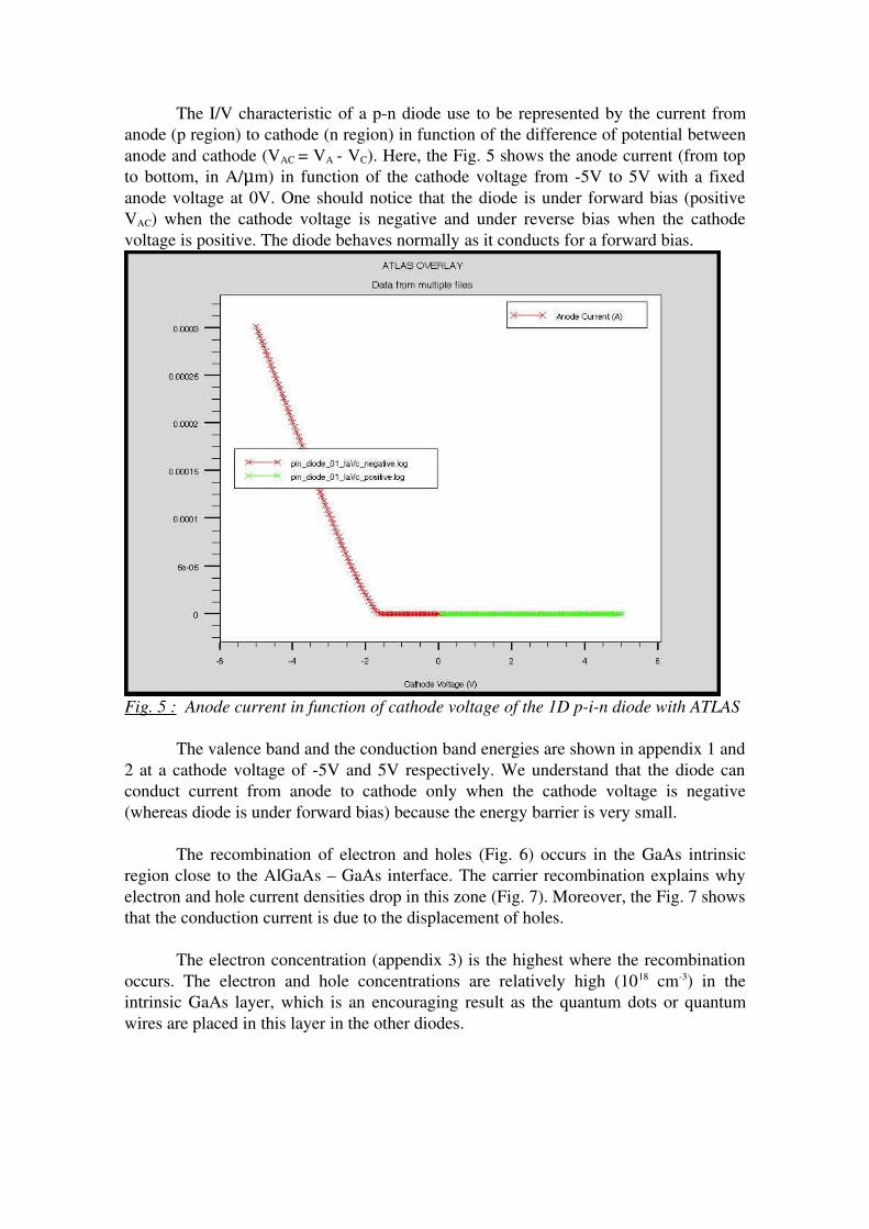
The I/V characteristic of a pn diode use to be represented by the current from anode (p region) to cathode (n region) in function of the difference of potential between anode and cathode (VAC = VA VC). Here, the Fig. 5 shows the anode current (from top to bottom, in A/ m) in function of the cathode voltage from 5V to 5V with a fixedμ anode voltage at 0V. One should notice that the diode is under forward bias (positive VAC) when the cathode voltage is negative and under reverse bias when the cathode voltage is positive. The diode behaves normally as it conducts for a forward bias.
Fig. 5 : Anode current in function of cathode voltage of the 1D pin diode with ATLAS
The valence band and the conduction band energies are shown in appendix 1 and 2 at a cathode voltage of 5V and 5V respectively. We understand that the diode can conduct current from anode to cathode only when the cathode voltage is negative (whereas diode is under forward bias) because the energy barrier is very small.
The recombination of electron and holes (Fig. 6) occurs in the GaAs intrinsic region close to the AlGaAs – GaAs interface. The carrier recombination explains why electron and hole current densities drop in this zone (Fig. 7). Moreover, the Fig. 7 shows that the conduction current is due to the displacement of holes.
The electron concentration (appendix 3) is the highest where the recombination occurs. The electron and hole concentrations are relatively high (1018 cm3) in the intrinsic GaAs layer, which is an encouraging result as the quantum dots or quantum wires are placed in this layer in the other diodes.

Fig. 6 : Recombination rate profile at Vc=5V of the 1D pin diode with ATLAS
Fig. 7 : Current density profiles at Vc=5V of the 1D pin diode with ATLAS

1.3 COMSOL Multiphysics results
In the COMSOL simulation, to be sure to obtain convergence in a reasonable computation time, the device width and the AlGaAs substrate thickness were reduced to 200 nm (which correspond respectively one tenth and one fifth of their initial size).
As all the material properties required for the simulation are not present in the COMSOL material libraries, the values from silvacoATLAS libraries were used for the intrinsic carrier concentration, electric permittivity, electron and hole diffusion coefficients, mobilities and lifetimes.
The Fig. 8 shows the absolute value of the doping profile along the device surface whereas the Fig. 9 represents the same doping level along device depth (the y axis is in the opposite direction compared to the ATLAS simulation). The anode is in contact with the p type region, at y = 0 m, and the cathode is in the diode backside, inμ contact with the n type substrate, at y = 3.5 m. μ
Fig. 8 : Absolute doping profile along the 1D pin diode surface with COMSOL

Fig. 9 : Absolute doping profile along the 1D pin diode depth with COMSOL
The anode current (in A/ m) in function of the cathode voltageμ (Vc in V) is shown with a logarithmic scale from 1 V to 0 V in Fig. 10 and with a linear scale from 0 V to 2V in Fig. 11. Even though the curve is different form the one obtained with ATLAS and the order of magnitude of the current value is surprisingly high, this is also the characteristic curve of a diode.

Fig. 10 : Anode current in function of Vc for Vc negative for the 1D pin diode with COMSOL, logarithmic scale
Fig. 11 : Anode current in function of Vc for Vc positive for the 1D pin diode with COMSOL, linear scale

The electron and hole concentration profiles along device depth for different values of negative cathode voltage are shown respectively appendix 4 and 5 whereas the recombination rate is plotted Fig. 12. Concerning the carrier concentration, the results found with COMSOL are quite different from the ones of ATLAS. This is probably due to the fact that several models such as electric field mobility dependency, auger recombination and band gap narrowing were used in the ATLAS simulation and not in the COMSOL one.
Fig. 12 : Recombination rate profile at different negative voltages of the 1D pin diode with COMSOL
Finally, both COMSOL and ATLAS simulations shows that the maximum of the recombination rate is situated in the intrinsic region, at the interface between AlGaAs and GaAs.

2. 2D pin diodes
In this chapter is presented the simulation results concerning three different kind of diodes fabricated at the IMM. These pin diodes are the GaAs bridge shape diode, the InP circular diode and the InP rectangular diode.
2.1 GaAs 2D bridge shape pin diode
The Fig. 13 is the model of a GaAs 2D pin diode. It shows the schematic lateral view of the device with its dimensions, composition and doping levels. In this diode, the quantum objects such as quantum wires (QW) or quantum dots (QD) are suppose to be placed in the middle of the intrinsic GaAs layer. In the Fig. 14, the structure of the simulated GaAs 2D pin diode is represented on scale. The electrodes are situated at the same position than in Fig. 13 but they are flat.
Fig. 13 : Schematic of the GaAs 2D bridge shape pin diode geometry
The I/V characteristic of the GaAs 2D bridge shape diode is showed in appendix 6. After threshold (below 1.2 V), the anode current increases linearly with the cathode voltage. In appendix 7, the band diagram of the GaAs 2D bridge shape diode at a cathode voltage of 5 V shows that holes can pass through the diode more easily than electrons as they do not face any potential barrier.

Fig. 14 : Structure of the GaAs 2D pin diode geometry with ATLAS
Fig. 15 :Conduction current density profile at Vc=5Vand for Ia=5*106A/ m withinμ the GaAs 2D bridge shape pin diode geometry with ATLAS
36% IMAX

Fig. 16 : Recombination rate profile at Vc=5V at Vc=5Vand for Ia=5*106A/ mμ within the GaAs 2D bridge shape pin diode geometry with ATLAS
The Fig. 15 and 16 show respectively the conduction current density and the recombination rate with the device for a total anode current of 5*106A/ m. In reality,μ the photonic crystal is the bridge of intrinsic GaAs between 1 and 2 m in theμ horizontal axis. The cavity is in the middle of this bridge. The main requirement for this diode is to inject carrier in the quantum dots that would be in the photonic crystal cavity, in middle of the bridge. The simulation shows that here is only 36 % of the maximum conduction current density which passes in the middle of the bridge. In this same place, there is 21 % of the maximum recombination rate.
This simulation shows that there is a rather poor efficiency of this diode geometry. Nevertheless, no quantum well was placed in the middle of the bridge to model the series of quantum objects. We expect that in the real device, carrier may be trapped in the quantum objects of the bridge. In this case, the percentage of the maximum conduction current density would be higher in the middle of the bridge. Therefore, this geometry does not have to be rejected and it be considered better than what this simulation shows.
21% RMAX

2.2 InP 2D circular pin diode
The InP 2D circular pin diode name comes from its real three dimensional shape. For instance the top view of the Fig. 17 shows that the anode is circular. As the simulation is in two dimensions only, the simulated system loses this circular symmetry and correspond to a vertical cut of the device along its diameter. The Fig. 17 shows the schematic lateral view of the device with its dimensions, composition and doping levels. This device has no suspended area. Hence, this device cannot include a photonic crystal. This diode is use to characterize the emission of quantum dots, quantum wires or other quantum objects which are placed in series instead of the InGaAs layer of the diode in Fig. 17. The InGaAs layer is actually used in the simulation to model the quantum objects series. The simulation aims to determine to which quantum objects the diode injects charge carriers.
Fig. 17 : Schematic of the InP 2D circular pin diode
The I/V characteristic of the InP 2D circular pin diode is showed in appendix 8 whereas the conduction current density profile in the device for a total anode current of 1*104 A/ m is represented in Fig. 18. At the bottom part of Fig. 18 is plotted aμ enlargement (in Y direction) of the upper picture. The scale and unit of the conduction current density is the same in both representations. We observe that the maximum current density is found in the lateral sides of the InGaAs well. The current density reach 23 % of its maximum in the p doped InP layer in the zone between 375 and 400
m from the center. In the intrinsic and n doped regions, the highest current density isμ located on the sides (from 350 to 450 m) and reaches only 1 % of the maximum. μ
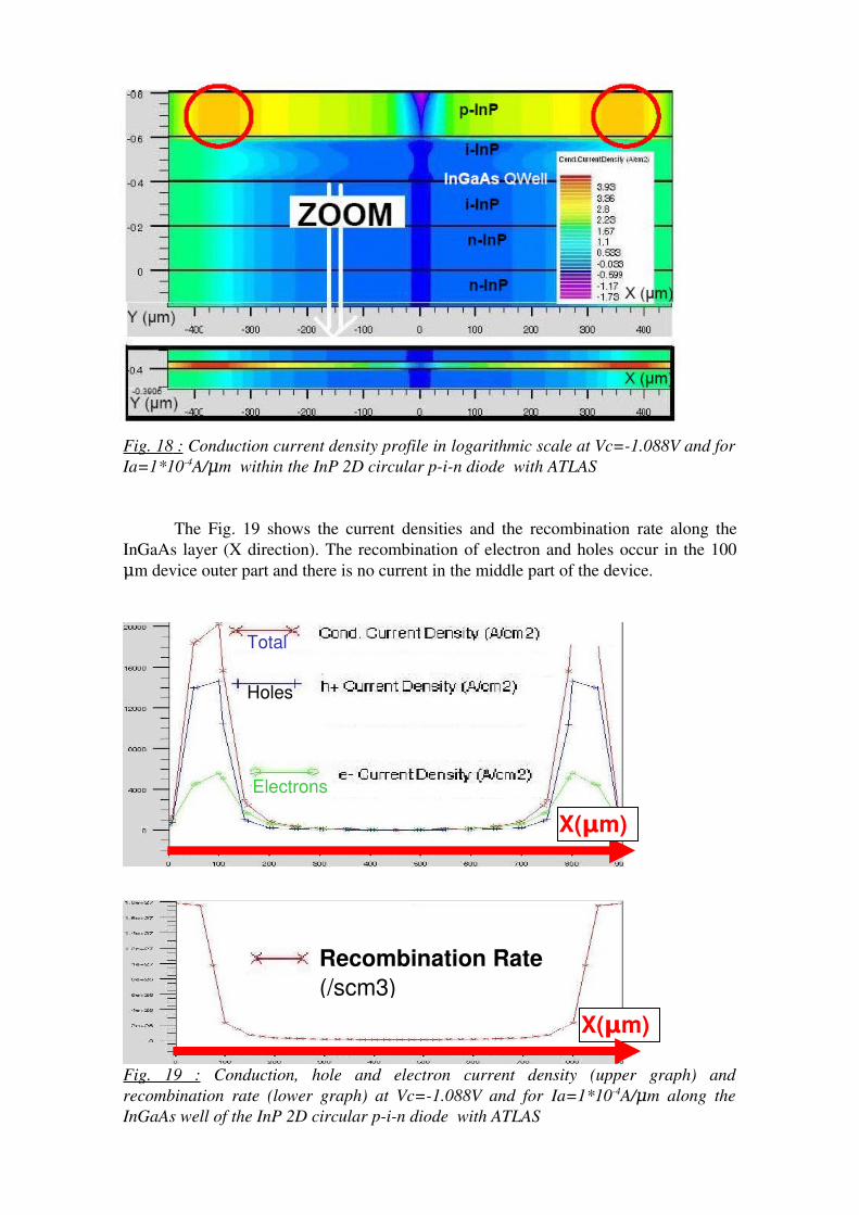
Fig. 18 : Conduction current density profile in logarithmic scale at Vc=1.088V and for Ia=1*104A/ mμ within the InP 2D circular pin diode with ATLAS
The Fig. 19 shows the current densities and the recombination rate along the InGaAs layer (X direction). The recombination of electron and holes occur in the 100
m device outer part and there is no current in the middle part of the device. μ
Fig. 19 : Conduction, hole and electron current density (upper graph) and recombination rate (lower graph) at Vc=1.088V and for Ia=1*104A/ mμ along the InGaAs well of the InP 2D circular pin diode with ATLAS
Total
Holes
Electrons
Recombination Rate (/scm3)
X(μm)
X(μm)

The InP 2D circular pin diode is not able to inject charge carriers to the quantum objects situated within 250 mμ radius disk whose center coincides with the diode center. A InP 2D circular pin diode with the same geometry and a diameter of 100 mμ (instead of 800 m in Fig. 17μ ) is supposed to inject carriers efficiently to all the quantum objects present in the device.
2.3 InP 2D rectangular pin diode
The InP rectangular pin diode is a three dimensional system which structure is shown in Fig. 20. This diode is used to characterize the emission of quantum dots within a photonic crystal structure. The InP rectangular pin diode has the same structure than the GaAs pin diode shown in Fig. 1 (but the material composition is different). As simulations are in two dimensions, this diode was simulated along two cuts shown in Fig. 21. Then, the influences of the device geometry, the position of electrodes and the device size on the current density repartition were studied for one cut.
Fig. 20 : Schema in 3D of the InP rectangular pin diode

Along the cut one (refer to Fig. 19) was simulated the diode called symmetric electrodes. Along the second cut, three diodes named 650 nm width, 550 nm width and antisymmetric electrodes where simulated to study the influence of diode geometry and one more diode called 5500 nm was computed to study the influence of device size.
Fig. 21 : Picture of one of the rectangular pin diode fabricated at IMM (CNMCSIC)
2.3.1 InP 2D rectangular pin diode – Symmetric electrodes
The Fig. 22 shows the schematic lateral view of the InP 2D rectangular pin diode with symmetric electrodes with its dimensions, composition and doping levels. In the appendix 9 is shown the I/V characteristic of this diode.
Fig. 22 : Schema of the InP 2D rectangular pin diode – Symmetric electrodes (dimensions in nm)

As the simulations of the InP rectangular pin diode correspond only to different cuts of the same device, the energy band diagram is the same for all. The energy band diagram of the InP 2D rectangular pin diode is shown in Fig. 23 for cathode voltage of Vc=1.33V. The InGaAs layer creates a high potential well in which electrons and holes are trapped and recombine.
Fig. 23 : Energy band diagram of the InP 2D rectangular pin diode at Vc=1.33V with ATLAS
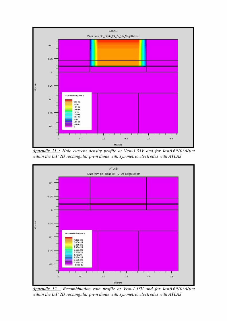
The Fig. 24 shows the current density profile within the device whereas the appendixes 10, 11 and 12 represent respectively the electron, hole current density and recombination rate profiles under the same conditions.
Fig. 24 : Conduction current density profile at Vc=1.33V and for Ia=6.6*105A/ mμ within the InP 2D rectangular pin diode with symmetric electrodes with ATLAS
Holes
Electrons
Recombination
in the well
Y (μm)
X (μm)
InP P InP I InGaAs InP I InP InGaAs
Anode CathodeE
C (eV)
EV
(eV)
Y (μm)

The energy band diagram explains that the holes cannot pass the potential well and go only from the p doped region to the well. As the conduction band energy has a smaller potential well height than the valence band energy, a part of electrons can pass the potential well and reach the anodes while the rest of electrons recombine with holes in the InGaAs layer.
For this diode, the electrode position of the output of the simulation does not to the program input (corresponding to the geometry in Fig. 22). Indeed, the cathodes are two points situated in x = 0 nm and x = 550 nm respectively. This explains why there is a higher current density on the sides of the ndoped region. Because of this bug, the current density value of this simulation cannot be compared with the other diodes. Nevertheless, the simulation of the InP 2D rectangular pin diode with symmetric electrodes shows that the current density and the recombination rate (refer to appendix 12) are constant along the X axis in the middle of the suspended structure (between the two anodes).
One can notice that the width of the InP 2D rectangular pin diode with symmetric electrodes is of the order of magnitude of the micrometer. At the contrary, the width of the InP circular diode is of the order of the millimeter. Besides, the simulation of the InP circular diode showed that the current density is not constant and at a high value along the X axis in the middle of the device. These two simulations show that the device size affects significantly the current density repartition.
2.3.2 InP 2D rectangular 650nm width pin diode
The Fig. 25 is the model of InP 2D rectangular 650nm width pin diode. It shows the schematic lateral view of the device with its dimensions, composition and doping levels. The appendix 13 shows the I/V characteristic of the same device.
In the Fig. 26, we can observe that the conduction current density within 650nm width diode is lower in the upper part of the photonic crystal than in the rest of the device. At the contrary, the current density in the well is slightly higher than in the rest of the device upper part.

Fig. 25 : Schema of the InP 2D rectangular 650 nm width pin diode (dimensions in nm)
Fig. 26 : Conduction current density profile at Vc=1.295V and for Ia=1*104A/ mμ within the InP 2D rectangular 650 nm pin diode with ATLAS
Photonic crystal position
Y (μm) X (μm)

2.3.3 InP 2D rectangular 550nm width pin diode
The Fig. 27 is the model of InP 2D rectangular 550nm width pin diode. It shows the schematic lateral view of the device with its dimensions, composition and doping levels. The appendix 14 shows the I/V characteristic of the same device. With this geometry, the idea is to concentrate the current in a smaller device and to increase the influence of the left part of the anode relatively to the right one.
In the Fig. 28, we can observe that the conduction current density is higher at the photonic crystal position within 550nm width diode than in the 650 nm one. This seems logical to have a higher current density in a smaller device.
Fig. 27 : Schema of the InP 2D rectangular 550 nm width pin diode (dimensions in nm)

Fig. 28 : Conduction current density profile at Vc=1.336V and for Ia=1*104A/ mμ within the InP 2D rectangular 550 nm width pin diode with ATLAS
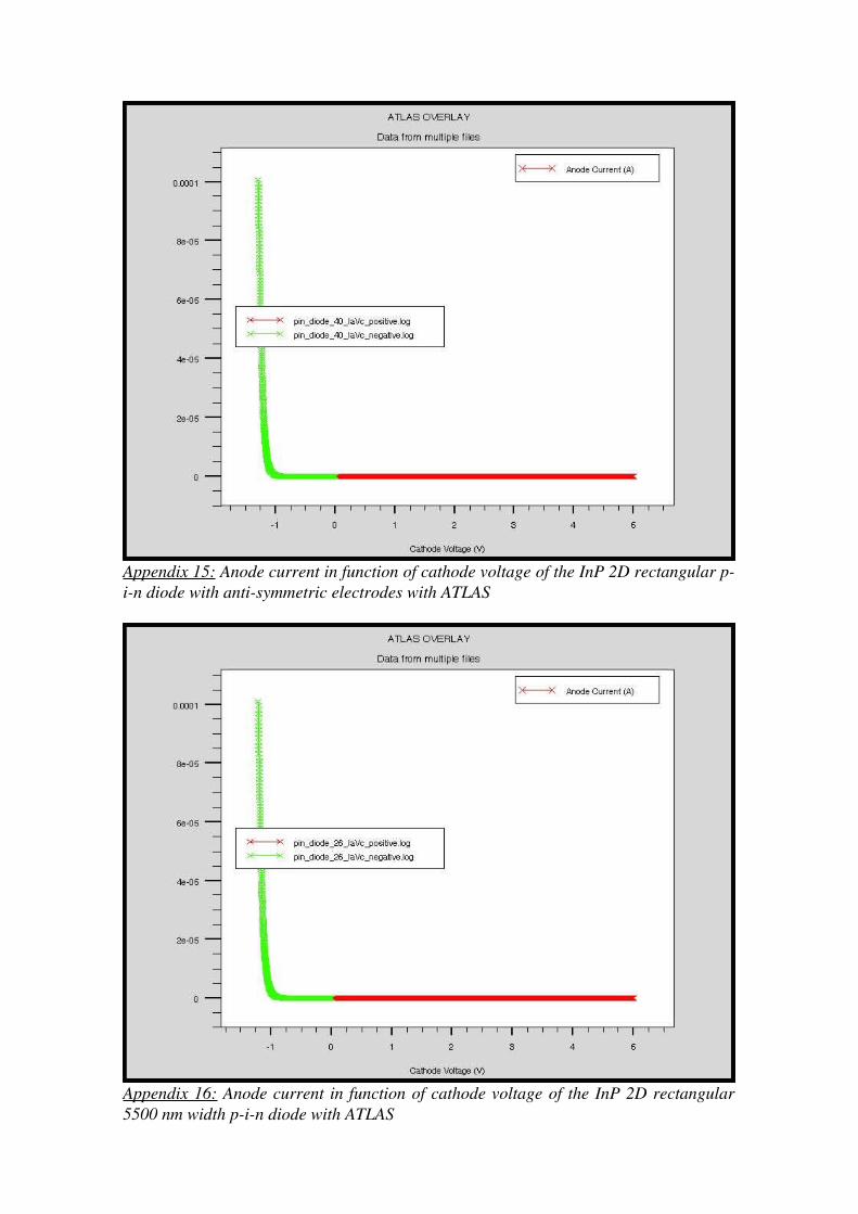
2.3.4 InP 2D rectangular pin diode – Antisymmetric electrodes
The Fig. 29 shows the schematic lateral view of the InP 2D rectangular pin diode with antisymmetric electrodes with its dimensions, composition and doping levels. In the appendix 15 is shown the I/V characteristic of this diode. With this diode, the objective is to increase the current density, where the photonic crystal is supposed to be, by driving some current from the left cathode to the right anode.
Photonic crystal position
Y X (μm)

Fig. 29 : Schema of the InP 2D rectangular pin diode – antisymmetric electrodes (dimensions in nm)
The main difference with other plots that can be seen in the Fig. 30 is that the conduction current density is higher close to the right part of the cathode.
Fig. 30 : Conduction current density profile at Vc=1.296V and for Ia=1*104A/ mμ within the InP 2D rectangular pin diode with antisymmetric electrodes with ATLAS
Photonic crystal position
Y X (μm)

2.3.5 InP 2D rectangular pin diode – geometry comparison
In order to be comparable, the conduction current density plots of the 650 nm width, 550 nm width and antisymmetric electrode diodes were taken for a total anode voltage of 1*104A/ m (the current unit is divided by a distance unit becauseμ simulations are in two dimensions). The Fig. 31 shows the conduction current density along the InGaAs layer of the three former systems.
Fig. 31 : Conduction current density along AlGaAs layer for Ia=1*104A/ m μ for the 650 nm width, 550 nm width and antisymmetric InP 2D rectangular pin diode with ATLASFig. 3 1 : Conduction current density along AlGaAs layer for Ia=1*104A/ m μ for the 650 nm width, 550 nm width and antisymmetric InP 2D rectangular pin diode with ATLAS
In the center of suspended part (where is supposed to be the photonic crystal cavity), there is 25 % more current density in the 550 nm width system relatively to the 650 nm one whereas the increase of current density is of 8 % only in the antisymmetric electrode geometry relatively to the 650 nm one. The 550 nm width diode geometry is supposed to inject the most charge carriers in the quantum dots of the photonic crystal cavity out of these three geometries.
geometría desde arriba
550 nm width diode
Antisymmetric diode
650 nmwidth diodePhotonic crystal
position
Conduction current density (A/cm2)
X (μm)
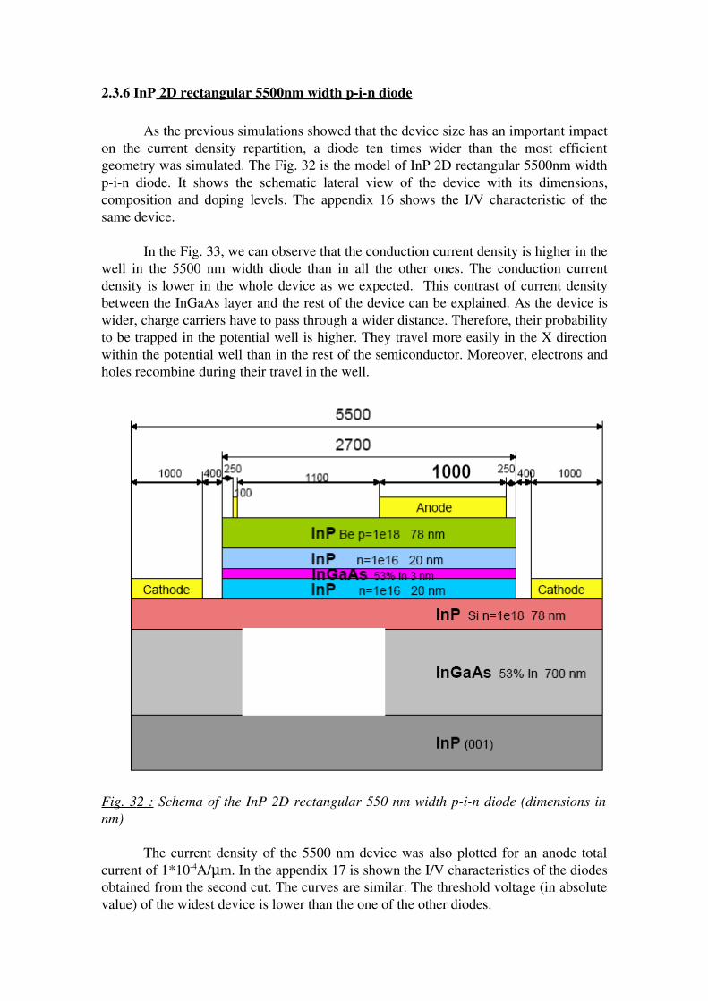
2.3.6 InP 2D rectangular 5500nm width pin diode
As the previous simulations showed that the device size has an important impact on the current density repartition, a diode ten times wider than the most efficient geometry was simulated. The Fig. 32 is the model of InP 2D rectangular 5500nm width pin diode. It shows the schematic lateral view of the device with its dimensions, composition and doping levels. The appendix 16 shows the I/V characteristic of the same device.
In the Fig. 33, we can observe that the conduction current density is higher in the well in the 5500 nm width diode than in all the other ones. The conduction current density is lower in the whole device as we expected. This contrast of current density between the InGaAs layer and the rest of the device can be explained. As the device is wider, charge carriers have to pass through a wider distance. Therefore, their probability to be trapped in the potential well is higher. They travel more easily in the X direction within the potential well than in the rest of the semiconductor. Moreover, electrons and holes recombine during their travel in the well.
Fig. 3 2 : Schema of the InP 2D rectangular 550 nm width pin diode (dimensions in nm)
The current density of the 5500 nm device was also plotted for an anode total current of 1*104A/ m. In the appendix 17 is shown the I/V characteristics of the diodesμ obtained from the second cut. The curves are similar. The threshold voltage (in absolute value) of the widest device is lower than the one of the other diodes.

Fig. 33 : Conduction current density profile at Vc=1.213V and for Ia=1*104A/ mμ within the InP 2D rectangular 5500 nm width pin diode with ATLAS
The Fig. 34 shows the conduction current density along the InGaAs layer of the 5500 nm width diode. In the center of suspended part (where is supposed to be the photonic crystal cavity), the current density is ten times higher that the one in the 550 nm width system and 12,5 times the one in the 650 nm width system.
Fig. 34 : Conduction current density along AlGaAs layer for Ia=1*104A/ m μ for the 5500 nm width InP 2D rectangular pin diode with ATLAS
Photonic crystal position
Y (μm)
X (μm)
Finally, the simulations of the InP rectangular pin diode show that the 5500 nm width diode has the geometry which is supposed to inject the most charge carriers in the quantum dots of the photonic crystal cavity out of the four simulated geometries.
3. Sum up and discussion of the results
3.1 Important remark
Because of misunderstandings, I realized only at the end of this internship that the GasAs bridge shape and the InP rectangular pin diodes I simulated have a different size than the actual diodes. For instance, the width of the real photonic crystals is of the order of magnitude of the millimeter. The fabricated InP rectangular pin diodes have the dimension values shown in the Fig. 25 but the unit of the lateral dimension is micrometer.
As the simulations showed that the repartition of current density is strongly dependent on the device width, the simulated GasAs bridge shape and InP rectangular pin diodes have most probably a different behavior than the real diodes. The former simulation of the GasAs bridge shape and InP rectangular pin diodes are not expected to predict the behavior of the fabricated diodes which are respectively hundred and thousand time wider than the simulated ones.
3.2 Result Summary
First, the simulation of pin diodes in one dimension allow me to understand how to exploit silvacoATLAS and COMSOL Multiphysics softwares. The 1D pin diode simulation showed that the recombination of electron and holes occurs in the GaAs intrinsic region close to the AlGaAs – GaAs interface.
The simulated GaAs bridge shape has a rather poor efficiency in terms of charge carriers injection in the suspended area. Nevertheless, as the quantum object series was not modeled, a real device of the same size should be more efficient than this one. However, the behavior of a fabricated GaAs bridge shape diode of an other width is supposed to be different than the one of this simulation.
The simulation showed that the InP circular pin diode is not able to inject charge carriers to the quantum objects situated within 250 mμ radius disk whose center coincides with the diode center. An InP circular pin diode with the same geometry and a diameter of 100 mμ is expected to inject carriers efficiently to all the quantum objects present in the device.
The InP rectangular diode simulations demonstrated that the current density repartition is strongly dependent from the system width. Moreover, the diode geometry or in other words the electrodes placement has a lower effect on the current density repartition than the device width. The 2D InP rectangular 5500 nm width pin diode is supposed to inject ten times more charge carriers in the quantum dots of the photonic crystal cavity than the other simulated geometries.

3.3 Future development
To obtain relevant results concerning the GaAs bridge shape and InP rectangular diodes, two more simulations should be carried on :
The GaAs bridge shape diode should be simulated with a wider width and with a thin layer of a lower energy band gap semiconductor in the middle of the intrinsic GaAs layer to model the quantum object series.
The InP rectangular diode should be simulated with a micrometer width (650 m total width instead of 650 nmμ ).
Conclusion
During this ten week internship at the IMM, three kind of pin diodes were simulated with the software SilvacoATLAS. The current density was shown along the device vertical cuts. Unfortunately, because of a misunderstanding, the study of the device geometry was carried on for smaller diodes than the real ones and the behavior of the fabricated devices cannot be predicted by considering the simulation results described in this report. Nevertheless, the simulations bring two relevant results.
First, the InP circular pin diode is not able to inject charge carriers to most of the quantum objects. An InP circular pin diode with the same geometry and a diameter of 100 m is expected to inject carriers efficiently to all the quantum objects present inμ the device.
Second, the current density repartition is strongly dependent on the system width and is less dependent on the diode geometry than on the device width.
Concerning SilvacoATLAS, it is an easy to use and powerful software to simulate two dimensional systems made of any semiconductor material. Indeed, the user can choose whether to use the default parameter models and material properties, whether to change these values, adapt models or integrate user defined models from experimental data to the simulation. My simulation files could be modified and exploited to obtain more relevant results.
This internship at the IMM allow me to learn how to use silvacoATLAS and to discover the work organization of a research institute.

Thanks
I would like to thank :
Pablo Aitor Postigo who permited me to achieve this work placement and followed my work,
Luisa González, Antonio Rivera and Iván Prieto for having had a look at my work and for their suggestions,
Clara Benedet for solving my computer problems so efficiently,all the persons from the MBE research group and from the IMM for welcoming
me and integrating me into their working team,
Philippe Rey from silvaco sales team for letting me use silvacoATLAS Ahmed Nejim from silvaco support team for checking my results
the COMSOL support team for helping me to resolve problems,
my professors from the Master Nanotech, Phelma and Grenoble INP for encouraging students to do summer internships.

Appendixes
Appendix 1 : Energy band diagram at Vc=5V of the 1D pin diode with ATLAS
Appendix 2 : Energy band diagram at Vc=5V of the 1D pin diode with ATLAS
GaAs P AlGaAs GaAs I GaAs N
GaAs P AlGaAs GaAs I GaAs N

Appendix 3 : Electron and hole concentration profiles at Vc=5V of the 1D pin diode with ATLAS
Appendix 4 : Electron concentration profile at different negative cathode voltages (in V) of the 1D pin diode with COMSOL

Appendix 5 : Hole concentration profile at different negative cathode voltages (in V) of the 1D pin diode with COMSOL
Appendix 6: Anode current in function of cathode voltage of the GaAs bridge shape pin diode with ATLAS

Appendix 7: Energy band diagram at Vc=5V of the GaAs bridge shape pin diode with ATLAS
Appendix 8: Anode current in function of cathode voltage of the InP 2D circular pin diode with ATLAS
EC (eV)
EV
(eV)
GaAs N GaAs I AlGaAs AlGaAs
GaAs P
Cathode
Holes
Anode

Appendix 9: Anode current in function of cathode voltage of the InP 2D rectangular pin diode with symmetric electrodes with ATLAS
Appendix 10 : Electron current density profile at Vc=1.33V and for Ia=6.6*105A/ mμ within the InP 2D rectangular pin diode with symmetric electrodes with ATLAS
Appendix 11 : Hole current density profile at Vc=1.33V and for Ia=6.6*105A/ mμ within the InP 2D rectangular pin diode with symmetric electrodes with ATLAS
Appendix 12 : Recombination rate profile at Vc=1.33V and for Ia=6.6*105A/ mμ within the InP 2D rectangular pin diode with symmetric electrodes with ATLAS

Appendix 13: Anode current in function of cathode voltage of the InP 2D rectangular 650 nm width pin diode with ATLAS
Appendix 14: Anode current in function of cathode voltage of the InP 2D rectangular 550 nm width pin diode with ATLAS
Appendix 15: Anode current in function of cathode voltage of the InP 2D rectangular pin diode with antisymmetric electrodes with ATLAS
Appendix 16: Anode current in function of cathode voltage of the InP 2D rectangular 5500 nm width pin diode with ATLAS

Appendix 17: Anode current in function of cathode voltage of the 650 nm, 550 nm and 5500 nm width as well as the antisymmetric electrode InP 2D rectangular pin diode with ATLAS


