Interfacing to Analog World - WordPress.com · •Introduction to Analog to digital Conversion •...
31
• Introduction to Analog to digital Conversion • Why Analog to Digital? • Basics of A/D Conversion. • A/D converter inside PIC16F887 • Related Problems Interfacing to Analog World Sensor Interfacing Prepared By- Mohammed Abdul Kader Assistant Professor, EEE, IIUC
-
Upload
nguyendiep -
Category
Documents
-
view
231 -
download
0
Transcript of Interfacing to Analog World - WordPress.com · •Introduction to Analog to digital Conversion •...
• Introduction to Analog to digital Conversion
• Why Analog to Digital?
• Basics of A/D Conversion.
• A/D converter inside PIC16F887
• Related Problems
Interfacing to Analog World Sensor Interfacing
Prepared By-
Mohammed Abdul Kader
Assistant Professor, EEE, IIUC

Lecture Materials on "Interfacing to Analog World", By- Mohammed Abdul Kader, Assistant Professor, EEE, IIUC 2
Introduction to Analog to digital Conversion
Signals in the real world are analog: light, sound, temperature, pressure, acceleration or
other phenomenon. So, real-world signals must be converted into digital, using a circuit
called ADC (Analog-to-Digital Converter), before they can be manipulated by digital
equipment.
When you scan a picture with a scanner what the scanner is doing is an analog-to-digital
conversion: it is taking the analog information provided by the picture (light) and
converting into digital.
When you record your voice on your computer, you are using an analog-to-digital
converter to convert your voice, which is analog, into digital information.
When an audio CD is recorded at a studio, once again analog-to-digital is taking place,
converting sounds into digital numbers that will be stored on the disc.
Whenever we need the analog signal back, the opposite conversion – digital-to-analog,
which is done by a circuit called DAC, Digital-to-Analog Converter – is needed. When
you play an audio CD, what the CD player is doing is reading digital information stored
on the disc and converting it back to analog so you can hear the audio.
Lecture Materials on "Interfacing to Analog World", By- Mohammed Abdul Kader, Assistant Professor, EEE, IIUC 3
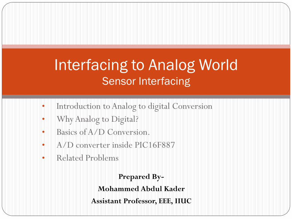
Why Analog to Digital? 1. Reducing Noise: Since analog signals can assume any value, noise is interpreted as
being part of the original signal. Digital systems, on the other hand, can only understand
two numbers, zero and one. Anything different from this is discarded.
Noise is added with
Signal
Information is
unchanged
Lecture Materials on "Interfacing to Analog World", By- Mohammed Abdul Kader, Assistant Professor, EEE, IIUC 4
Why Analog to Digital? (Continued)
2. Signal Processing: The most strong tool of processing or analyzing signal is
microprocessor. Microprocessor is a digital device. It can understand only digital signal. So,
we should convert the analog physical parameters into digital to process it by microprocessor.
3. Data compression capability: Another advantage of digital system against analog is the
data compression capability. Since the digital counterpart of an analog signal is just a bunch of
numbers, these numbers can be compressed, just like you would compress a Word file using
WinZip to shrink down the file size, for example. The compression can be done to save
storage space or bandwidth.
Lecture Materials on "Interfacing to Analog World", By- Mohammed Abdul Kader, Assistant Professor, EEE, IIUC 5
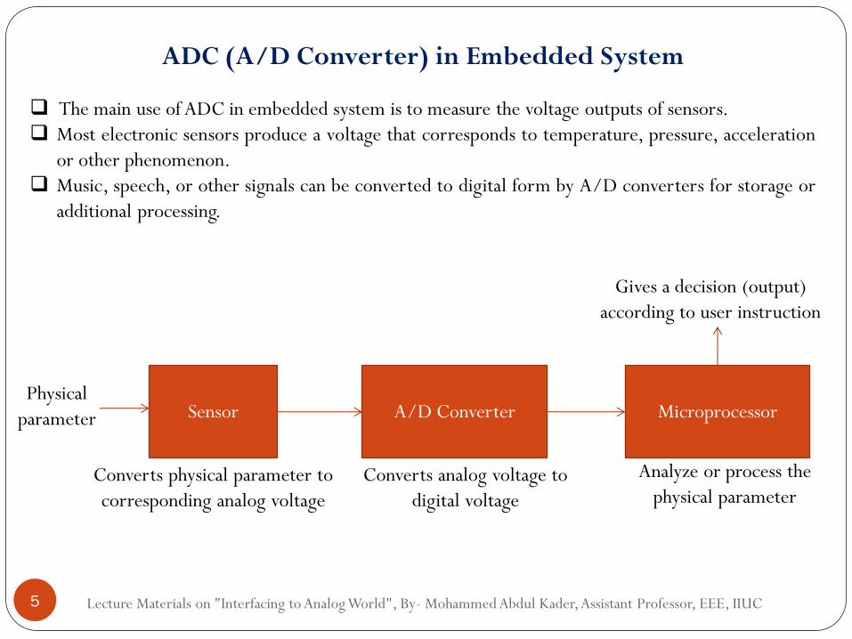
The main use of ADC in embedded system is to measure the voltage outputs of sensors.
Most electronic sensors produce a voltage that corresponds to temperature, pressure, acceleration
or other phenomenon.
Music, speech, or other signals can be converted to digital form by A/D converters for storage or
additional processing.
ADC (A/D Converter) in Embedded System
Sensor Physical
parameter A/D Converter
Converts physical parameter to
corresponding analog voltage
Converts analog voltage to
digital voltage
Microprocessor
Analyze or process the
physical parameter
Gives a decision (output)
according to user instruction
Lecture Materials on "Interfacing to Analog World", By- Mohammed Abdul Kader, Assistant Professor, EEE, IIUC 6
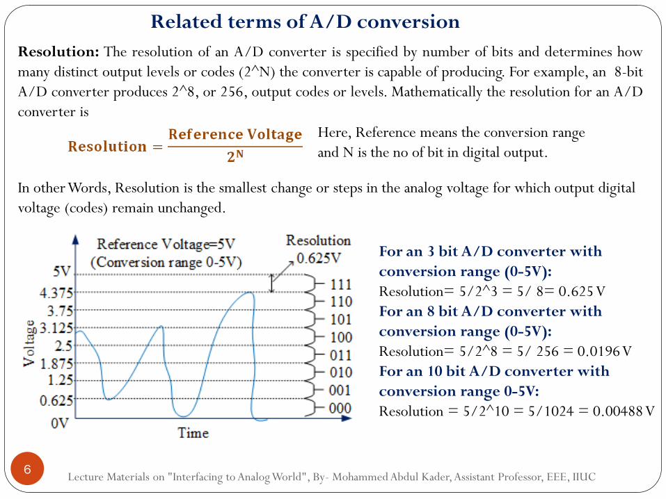
Related terms of A/D conversion
Resolution: The resolution of an A/D converter is specified by number of bits and determines how
many distinct output levels or codes (2^N) the converter is capable of producing. For example, an 8-bit
A/D converter produces 2^8, or 256, output codes or levels. Mathematically the resolution for an A/D
converter is
In other Words, Resolution is the smallest change or steps in the analog voltage for which output digital
voltage (codes) remain unchanged.
For an 3 bit A/D converter with
conversion range (0-5V):
Resolution= 5/2^3 = 5/ 8= 0.625 V
For an 8 bit A/D converter with
conversion range (0-5V):
Resolution= 5/2^8 = 5/ 256 = 0.0196 V
For an 10 bit A/D converter with
conversion range 0-5V:
Resolution = 5/2^10 = 5/1024 = 0.00488 V
Here, Reference means the conversion range
and N is the no of bit in digital output.

Lecture Materials on "Interfacing to Analog World", By- Mohammed Abdul Kader, Assistant Professor, EEE, IIUC 7
Related terms of A/D conversion (Cont.)
Resolution of an 2-bit A/D converter is 1.25V
Resolution of an 10-bit A/D converter is 0.00488V
Another definition ,The resolution of the A/D converter is the voltage change that will result in the
returned value (output digital value) changing by 1.
This means that with an 3 bit A/D the returned value will change by 1 when the voltage changes by
about 1.25V. With a 10 bit A/D, a change of only 4.88 mV will change the count by 1.

Lecture Materials on "Interfacing to Analog World", By- Mohammed Abdul Kader, Assistant Professor, EEE, IIUC 8
Clearly an A/D converter with more bits will give better accuracy.
But, for a higher bit A/D converter you need more storage memory to store the result and at the
same time A/D converter circuit become more complex and conversion time will increase.
Related terms of A/D conversion (Cont.)
Problem 1: A weight sensor changes its output voltage 0.1 mV for 1gm change in input and it’s
output varies from 0-5V. What should be the resolution and no of bits in the A/D converter if you
want to get the weight in gram.
The resolution should be 0.1mV = 0.0001 V
Lecture Materials on "Interfacing to Analog World", By- Mohammed Abdul Kader, Assistant Professor, EEE, IIUC 9
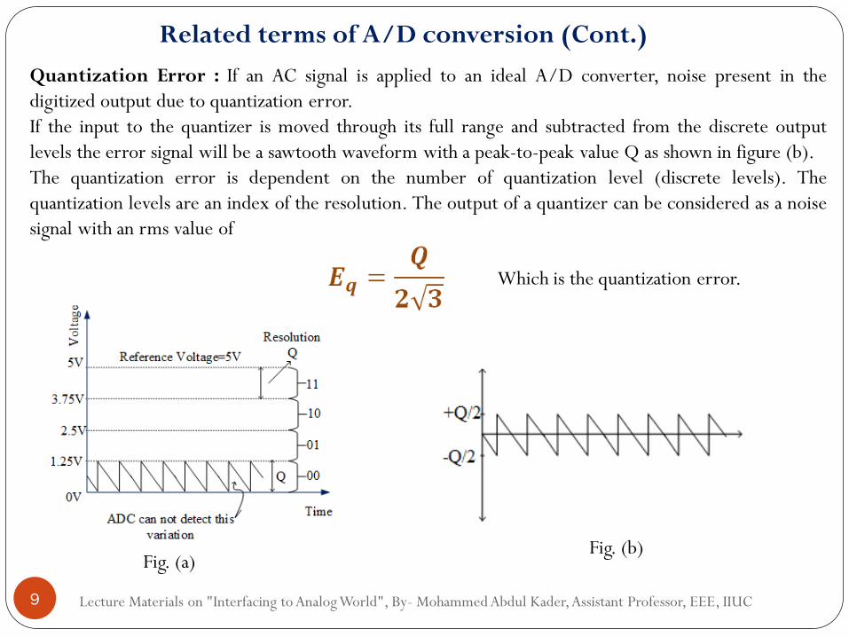
Related terms of A/D conversion (Cont.)
Quantization Error : If an AC signal is applied to an ideal A/D converter, noise present in the
digitized output due to quantization error.
If the input to the quantizer is moved through its full range and subtracted from the discrete output
levels the error signal will be a sawtooth waveform with a peak-to-peak value Q as shown in figure (b).
The quantization error is dependent on the number of quantization level (discrete levels). The
quantization levels are an index of the resolution. The output of a quantizer can be considered as a noise
signal with an rms value of
Which is the quantization error.
Fig. (a) Fig. (b)
Lecture Materials on "Interfacing to Analog World", By- Mohammed Abdul Kader, Assistant Professor, EEE, IIUC 10
Related terms of A/D conversion (Cont.)
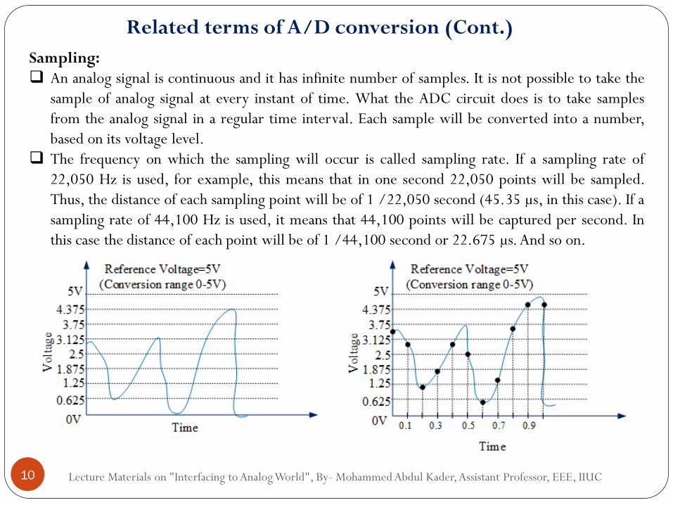
Sampling:
An analog signal is continuous and it has infinite number of samples. It is not possible to take the
sample of analog signal at every instant of time. What the ADC circuit does is to take samples
from the analog signal in a regular time interval. Each sample will be converted into a number,
based on its voltage level.
The frequency on which the sampling will occur is called sampling rate. If a sampling rate of
22,050 Hz is used, for example, this means that in one second 22,050 points will be sampled.
Thus, the distance of each sampling point will be of 1 /22,050 second (45.35 µs, in this case). If a
sampling rate of 44,100 Hz is used, it means that 44,100 points will be captured per second. In
this case the distance of each point will be of 1 /44,100 second or 22.675 µs. And so on.
Lecture Materials on "Interfacing to Analog World", By- Mohammed Abdul Kader, Assistant Professor, EEE, IIUC 11
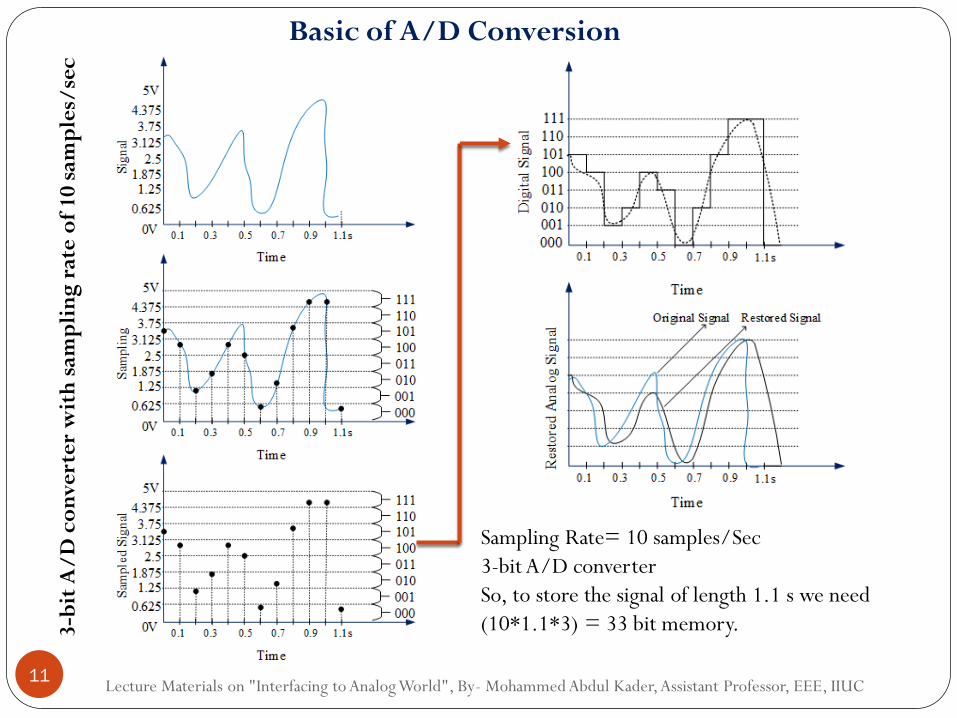
Basic of A/D Conversion
Sampling Rate= 10 samples/Sec
3-bit A/D converter
So, to store the signal of length 1.1 s we need
(10*1.1*3) = 33 bit memory. 3-b
it A
/D
co
nv
ert
er
wit
h s
amp
lin
g r
ate
of
10 s
amp
les/
sec

Lecture Materials on "Interfacing to Analog World", By- Mohammed Abdul Kader, Assistant Professor, EEE, IIUC 12
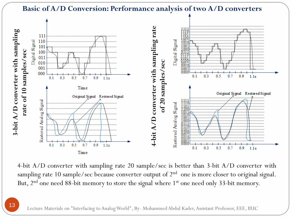
Sampling Rate= 20 samples/Sec
4-bit A/D converter
So, to store the signal of length 1.1 s we need
(20*1.1*4) = 88 bit memory. = 11 Byte 4-b
it A
/D
co
nv
ert
er
wit
h s
amp
lin
g r
ate
of
20 s
amp
les/
sec
Basic of A/D Conversion
Lecture Materials on "Interfacing to Analog World", By- Mohammed Abdul Kader, Assistant Professor, EEE, IIUC 13
Basic of A/D Conversion: Performance analysis of two A/D converters
4-b
it A
/D
co
nv
ert
er
wit
h s
amp
lin
g r
ate
of
20 s
amp
les/
sec
3-b
it A
/D
co
nv
ert
er
wit
h s
amp
lin
g
rate
of
10 s
amp
les/
sec
4-bit A/D converter with sampling rate 20 sample/sec is better than 3-bit A/D converter with
sampling rate 10 sample/sec because converter output of 2nd one is more closer to original signal.
But, 2nd one need 88-bit memory to store the signal where 1st one need only 33-bit memory.

Lecture Materials on "Interfacing to Analog World", By- Mohammed Abdul Kader, Assistant Professor, EEE, IIUC 14
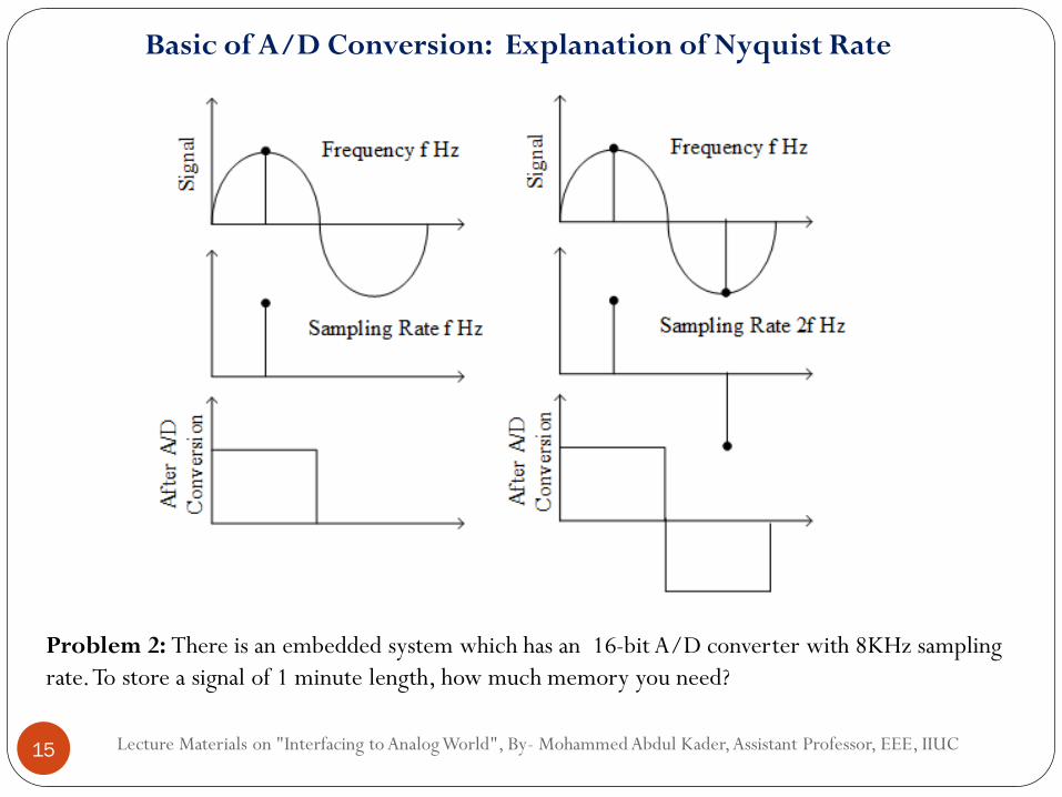
Basic of A/D Conversion: Minimum Sampling Rate (Nyquist Rate)
So, we have this dilemma: if the sampling rate is too high, the output quality will be close to
perfection, but you will need a lot of storage space to hold the generated data (i.e., the generated file
will be very big); if the sampling rate is too low, the output quality will be bad.
How can you know the best sampling rate to be used during analog-to-digital conversions to have the
best storage/quality balance? The answer is the Nyquist Theorem.
“This theorem states that the sampling rate on analog-to-digital conversions must
be at least two times the value of the highest frequency you want to capture.”
In practice it is necessary to sample at least 5 times the value of the highest frequency in order to
reduce the effect of noise and non-sinusoidal filters.
Since the human ear listens to sounds up to the frequency of 20 kHz, for music we need to use a
sampling rate of at least 40,000 Hz. In fact, the CD uses a 44,100 Hz sampling rate, thus capturing
more than our ears can hear (this value was arbitrated by Phillips and Sony when they created the
CD). Some professional audio applications use an even higher sampling rate.
The phone system, on the other hand, was created to transmit only human voice, which has a lower
frequency range, up to 4 kHz. So on the digital part of the phone system, an 8,000 Hz sampling rate
is used. That’s why if you try to transmit music through the phone the quality is bad: the phone
circuitry cancels all frequencies above 4 kHz.
Lecture Materials on "Interfacing to Analog World", By- Mohammed Abdul Kader, Assistant Professor, EEE, IIUC 15
Problem 2: There is an embedded system which has an 16-bit A/D converter with 8KHz sampling
rate. To store a signal of 1 minute length, how much memory you need?
Basic of A/D Conversion: Explanation of Nyquist Rate

Lecture Materials on "Interfacing to Analog World", By- Mohammed Abdul Kader, Assistant Professor, EEE, IIUC 16
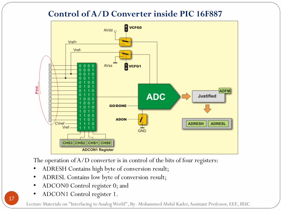
ANALOG MODULES of PIC16F887
Features of Analog Modules:
The A/D converter module has the following features:
The converter generates a 10-bit binary result using the method of successive approximation and
stores the conversion results into the ADC registers (ADRESL and ADRESH);
There are 14 separate analog inputs;
The A/D converter converts an analog input signal into a 10-bit binary number;
The minimum resolution or quality of conversion may be adjusted to various needs by selecting
voltage references Vref- and Vref+.
Lecture Materials on "Interfacing to Analog World", By- Mohammed Abdul Kader, Assistant Professor, EEE, IIUC 17
The operation of A/D converter is in control of the bits of four registers:
• ADRESH Contains high byte of conversion result;
• ADRESL Contains low byte of conversion result;
• ADCON0 Control register 0; and
• ADCON1 Control register 1.
Control of A/D Converter inside PIC 16F887

Lecture Materials on "Interfacing to Analog World", By- Mohammed Abdul Kader, Assistant Professor, EEE, IIUC 18
ADRESH and ADRESL Registers
The result obtained after converting an analog value into digital is a10-bit number that is to be
stored in the ADRESH and ADRESL registers.
There are two ways of handling it - left and right justification which simplifies its use to a great
extent. The format of conversion result depends on the ADFM bit of the ADCON1 register. In the
event that the A/D converter is not used, these registers may be used as general-purpose registers.
Control of A/D CONVERTER inside PIC 16F887 (Cont.)
Lecture Materials on "Interfacing to Analog World", By- Mohammed Abdul Kader, Assistant Professor, EEE, IIUC 19
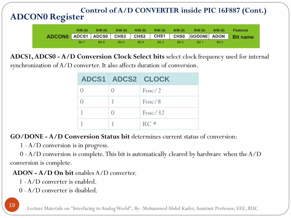
ADCON0 Register
ADCS1, ADCS0 - A/D Conversion Clock Select bits select clock frequency used for internal
synchronization of A/D converter. It also affects duration of conversion.
ADCS1 ADCS2 CLOCK
0 0 Fosc/2
0 1 Fosc/8
1 0 Fosc/32
1 1 RC *
GO/DONE - A/D Conversion Status bit determines current status of conversion:
1 - A/D conversion is in progress.
0 - A/D conversion is complete. This bit is automatically cleared by hardware when the A/D
conversion is complete.
Control of A/D CONVERTER inside PIC 16F887 (Cont.)
ADON - A/D On bit enables A/D converter.
1 - A/D converter is enabled.
0 - A/D converter is disabled.
Lecture Materials on "Interfacing to Analog World", By- Mohammed Abdul Kader, Assistant Professor, EEE, IIUC 20
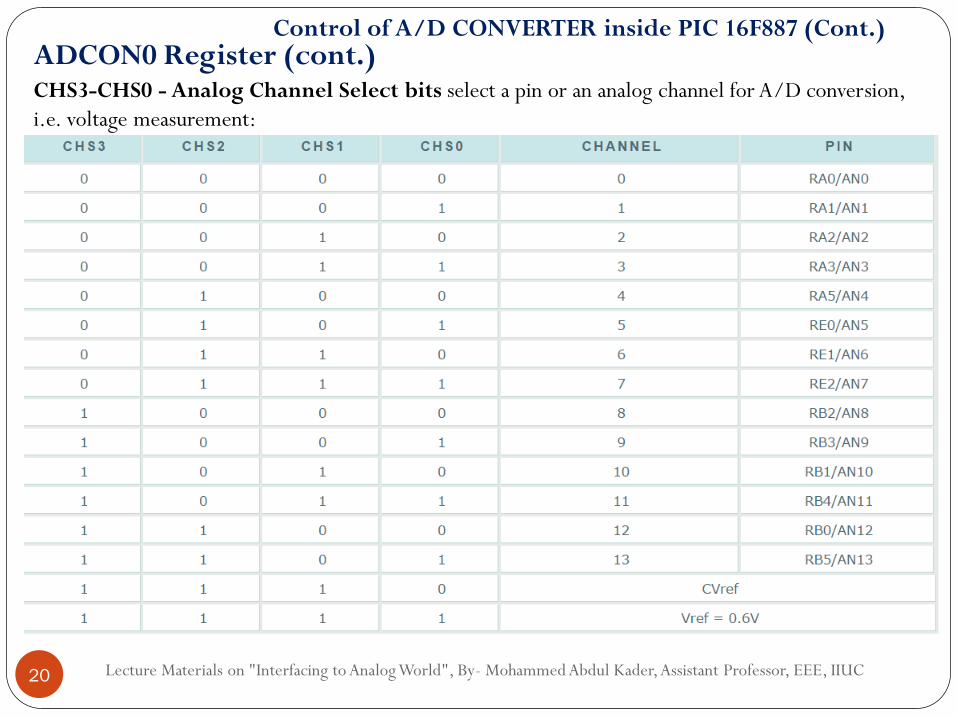
Control of A/D CONVERTER inside PIC 16F887 (Cont.)
CHS3-CHS0 - Analog Channel Select bits select a pin or an analog channel for A/D conversion,
i.e. voltage measurement:
ADCON0 Register (cont.)
Lecture Materials on "Interfacing to Analog World", By- Mohammed Abdul Kader, Assistant Professor, EEE, IIUC 21
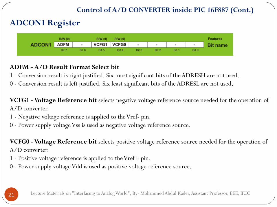
ADFM - A/D Result Format Select bit
1 - Conversion result is right justified. Six most significant bits of the ADRESH are not used.
0 - Conversion result is left justified. Six least significant bits of the ADRESL are not used.
VCFG1 - Voltage Reference bit selects negative voltage reference source needed for the operation of
A/D converter.
1 - Negative voltage reference is applied to the Vref- pin.
0 - Power supply voltage Vss is used as negative voltage reference source.
VCFG0 - Voltage Reference bit selects positive voltage reference source needed for the operation of
A/D converter.
1 - Positive voltage reference is applied to the Vref+ pin.
0 - Power supply voltage Vdd is used as positive voltage reference source.
Control of A/D CONVERTER inside PIC 16F887 (Cont.)
ADCON1 Register
Lecture Materials on "Interfacing to Analog World", By- Mohammed Abdul Kader, Assistant Professor, EEE, IIUC 22
A/D ACQUISITION REQUIREMENTS
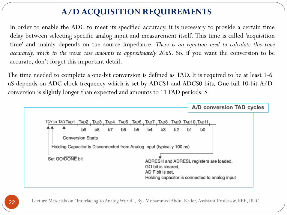
In order to enable the ADC to meet its specified accuracy, it is necessary to provide a certain time
delay between selecting specific analog input and measurement itself. This time is called 'acquisition
time' and mainly depends on the source impedance. There is an equation used to calculate this time
accurately, which in the worst case amounts to approximately 20uS. So, if you want the conversion to be
accurate, don’t forget this important detail.
The time needed to complete a one-bit conversion is defined as TAD. It is required to be at least 1-6
uS depends on ADC clock frequency which is set by ADCS1 and ADCS0 bits. One full 10-bit A/D
conversion is slightly longer than expected and amounts to 11 TAD periods. S
Lecture Materials on "Interfacing to Analog World", By- Mohammed Abdul Kader, Assistant Professor, EEE, IIUC 23
In order to measure voltage on an input pin by the A/D converter, the following should be done:
Step 1 - Port configuration:
• Write a logic one (1) to a bit of the TRIS register, thus configuring the appropriate pin as an
input.
• Write a logic one (1) to a bit of the ANSEL register, thus configuring the appropriate pin as an
analog input.
Step 2 - ADC module configuration:
• Configure voltage reference in the ADCON1 register.
• Select ADC conversion clock in the ADCON0 register.
• Select one of input channels CH0-CH13 of the ADCON0 register.
• Select data format using the ADFM bit of the ADCON1 register.
• Enable A/D converter by setting the ADON bit of the ADCON0 register.
Step 3 - ADC interrupt configuration (optionally):
• Clear the ADIF bit.
• Set the ADIE, PEIE and GIE bits.
Steps of using A/D Module
Lecture Materials on "Interfacing to Analog World", By- Mohammed Abdul Kader, Assistant Professor, EEE, IIUC 24
Step 4 - Wait for the required acquisition time to pass (approximately 20uS).
Step 5 - Start conversion by setting the GO/DONE bit of the ADCON0 register.
Step 6 - Wait for ADC conversion to complete.
• It is necessary to check in the program loop whether the GO/DONE pin is cleared or wait for
an A/D interrupt (must be previously enabled).
Step 7 - Read ADC results:
• Read the ADRESH and ADRESL registers.
Steps of using A/D Module (Cont.)
Lecture Materials on "Interfacing to Analog World", By- Mohammed Abdul Kader, Assistant Professor, EEE, IIUC 25
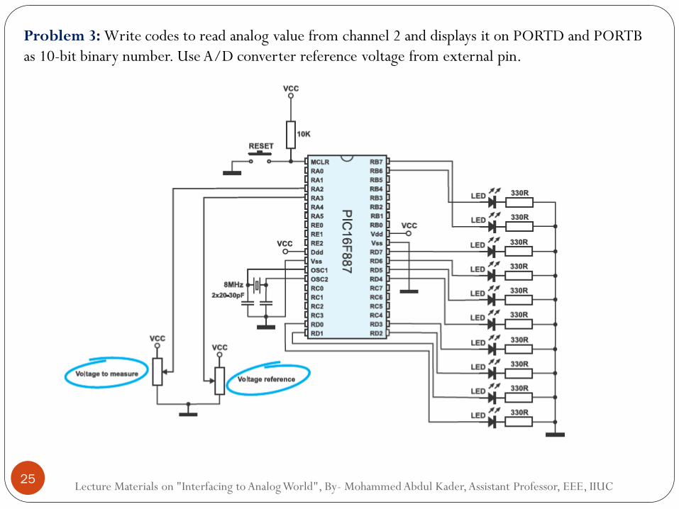
Problem 3: Write codes to read analog value from channel 2 and displays it on PORTD and PORTB
as 10-bit binary number. Use A/D converter reference voltage from external pin.

Lecture Materials on "Interfacing to Analog World", By- Mohammed Abdul Kader, Assistant Professor, EEE, IIUC 26
unsigned int temp_res;
void main() {
ANSEL = 0x0C; // Pins AN2 and AN3 are configured as analog
TRISA = 0xFF; // All port A pins are configured as inputs
ANSELH = 0; // Rest of pins is configured as digital
TRISB = 0x3F; // Port B pins RB7 and RB6 are configured as outputs
TRISD = 0; // All port D pins are configured as outputs
ADCON1.F4 = 1 ; // Voltage reference is brought to the RA3 pin.
do {
temp_res = ADC_Read(2); // Result of A/D conversion is copied to temp_res
PORTD = temp_res; // 8 LSBs are moved to port D
PORTB = temp_res >> 2; // 2 MSBs are moved to bits RB6 and RB7
} while(1); // Endless loop
}
In order to make this example work properly, it is necessary to tick off the ADC library in
the Library Manager prior to compiling:
• ADC
Solution of Problem 3
Lecture Materials on "Interfacing to Analog World", By- Mohammed Abdul Kader, Assistant Professor, EEE, IIUC 27
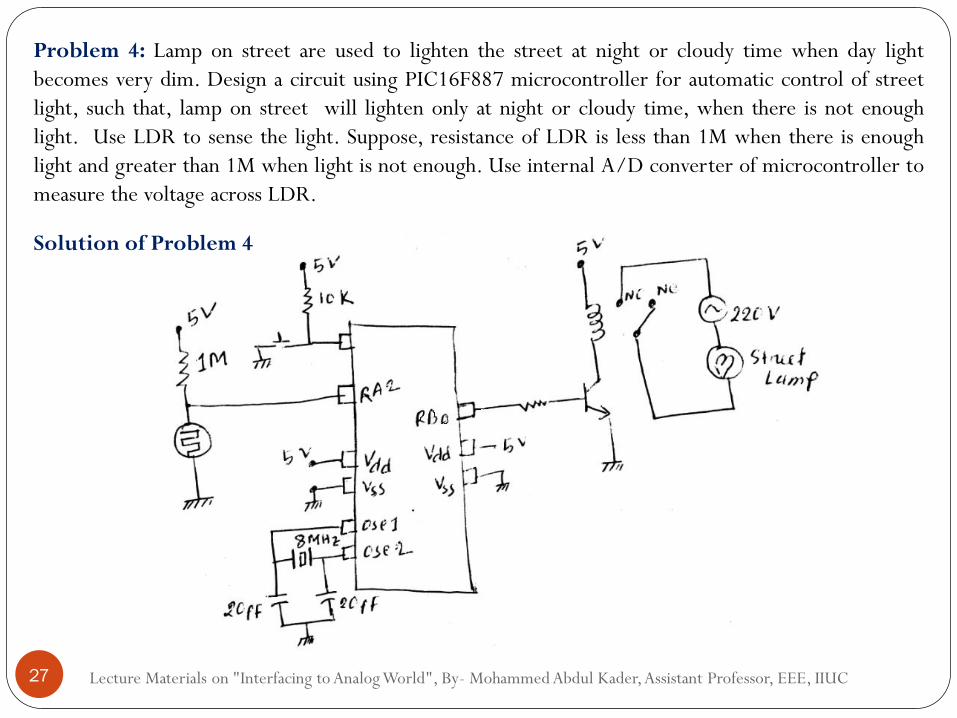
Problem 4: Lamp on street are used to lighten the street at night or cloudy time when day light
becomes very dim. Design a circuit using PIC16F887 microcontroller for automatic control of street
light, such that, lamp on street will lighten only at night or cloudy time, when there is not enough
light. Use LDR to sense the light. Suppose, resistance of LDR is less than 1M when there is enough
light and greater than 1M when light is not enough. Use internal A/D converter of microcontroller to
measure the voltage across LDR.
Solution of Problem 4

Lecture Materials on "Interfacing to Analog World", By- Mohammed Abdul Kader, Assistant Professor, EEE, IIUC 28
unsigned int light;
void main() {
ANSEL = 0x04; // Pins AN2 is configured as analog
TRISA = 0xFF; // All port A pins are configured as inputs
ANSELH = 0; // Rest of pins is configured as digital
TRISB.F0 =0; // Port B pin PB0 is configured as output
ADCON1.F4 = 0 ; // Power supply voltage Vdd is used as positive voltage reference source.
ADCON.F5=0; // Power supply voltage Vss is used as negative voltage reference source.
while(1)
{
light= ADC_Read(2); // Result of A/D conversion is copied to light
if(light>512)
PORTB.F0=1;
else PORTB.F0=0;
}
}
Program (Problem-4)
Lecture Materials on "Interfacing to Analog World", By- Mohammed Abdul Kader, Assistant Professor, EEE, IIUC 29
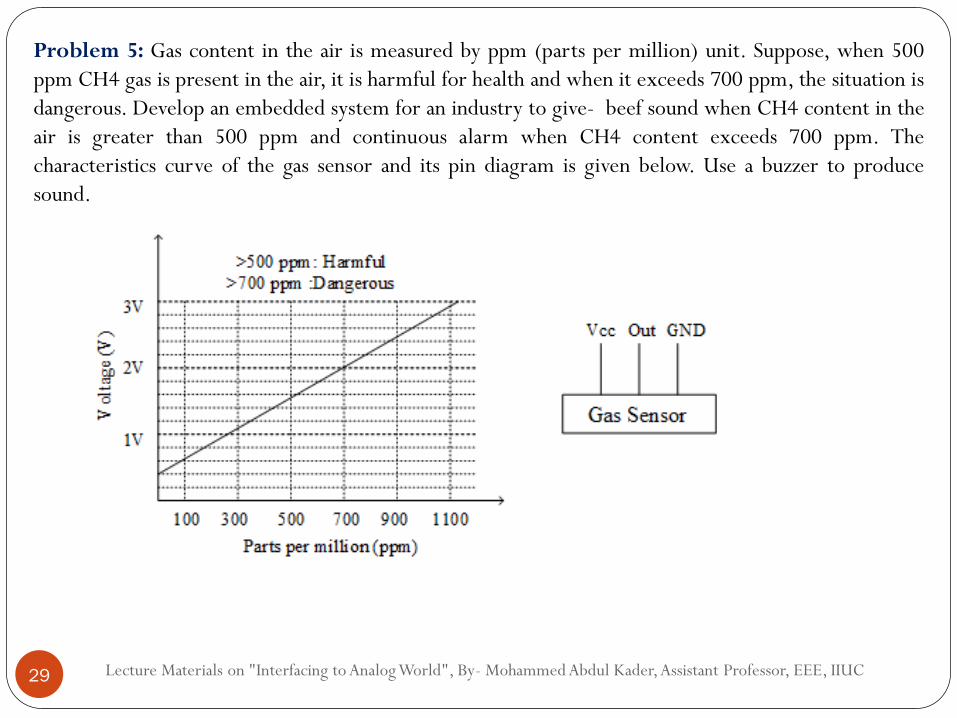
Problem 5: Gas content in the air is measured by ppm (parts per million) unit. Suppose, when 500
ppm CH4 gas is present in the air, it is harmful for health and when it exceeds 700 ppm, the situation is
dangerous. Develop an embedded system for an industry to give- beef sound when CH4 content in the
air is greater than 500 ppm and continuous alarm when CH4 content exceeds 700 ppm. The
characteristics curve of the gas sensor and its pin diagram is given below. Use a buzzer to produce
sound.
Lecture Materials on "Interfacing to Analog World", By- Mohammed Abdul Kader, Assistant Professor, EEE, IIUC 30
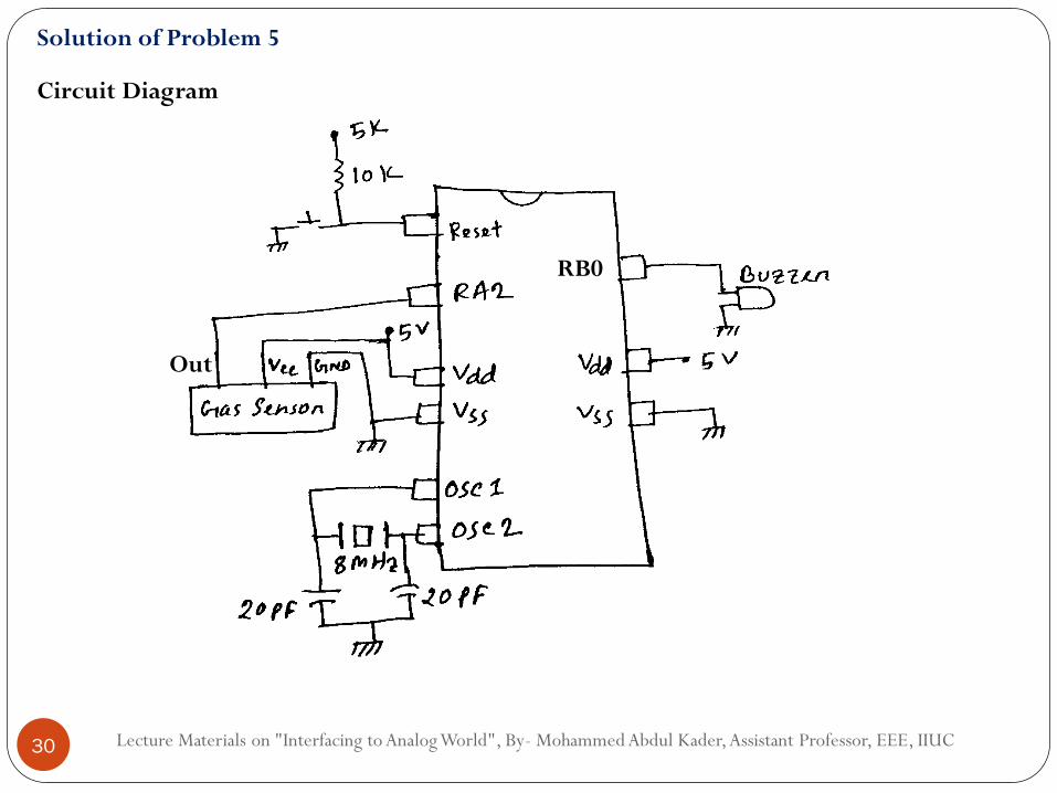
Solution of Problem 5
Circuit Diagram
Out
RB0
Lecture Materials on "Interfacing to Analog World", By- Mohammed Abdul Kader, Assistant Professor, EEE, IIUC 31
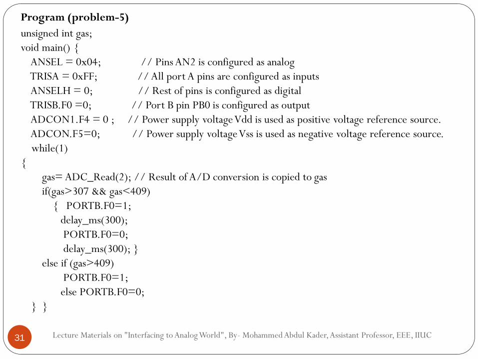
unsigned int gas;
void main() {
ANSEL = 0x04; // Pins AN2 is configured as analog
TRISA = 0xFF; // All port A pins are configured as inputs
ANSELH = 0; // Rest of pins is configured as digital
TRISB.F0 =0; // Port B pin PB0 is configured as output
ADCON1.F4 = 0 ; // Power supply voltage Vdd is used as positive voltage reference source.
ADCON.F5=0; // Power supply voltage Vss is used as negative voltage reference source.
while(1)
{
gas= ADC_Read(2); // Result of A/D conversion is copied to gas
if(gas>307 && gas<409)
{ PORTB.F0=1;
delay_ms(300);
PORTB.F0=0;
delay_ms(300); }
else if (gas>409)
PORTB.F0=1;
else PORTB.F0=0;
} }
Program (problem-5)