
Interfacial reactions and bump reliability of various pb...
8
Interfacial Reactions and Bump Reliability of Various Pb-Free Solder Bumps on Electroless Ni-P UBMs Kyung-Wook Paik, Young-Doo Jeon, and Moon-Gi Cho Department of Materials Science and Engineering Korea Advanced Institute of Science and Technology 373-1, Kusong-Dong, Yusong-Gu, Taejon, 305-701, Korea Tel) 042-869-3375 Abstract Electroless Ni-P UBMs combined with screen-printing of solder pastes are one of the low cost flip-chip bumping techniques. Pb-free solder bumps on electroless Ni-P UBM can be easily fabricated because various Pb-free solder alloy pas1es are available. Therefore, studies on interfacial reactions between electroless Ni-P UBM and Pb-free solders should be invcstigated, because they are greatly affected by small amount of alloying such as Ag, Cu, and Bi in Pb-free solders. Re1lability of Pb-free solder bumps can be greatly affected by intermetallic growth and P-rich Ni layer at the interface. Recently, Pb-free solder alloys such as SnAg, SnAgCu, SnCu, and SnAgBi have been suggested for promising candidates for substituting Sn37Pb solder. In this study, these four alloys were selected as solder bump materials for electroless Ni-P UBM. The effects of Ag, Cu, and Bi in Pb-free alloys on interfacial reactions and bump reliability at electroless Ni- P/scilder interfaces were investigated. Jt was found that the consumption rate of Ni-P UBM was much slower in SnAgCu and SnCu alloys than in SnAg and SnAgBi alloys during solder reflowing. And, SnAgCu and SnC U solders also showed lower Ni-P UBM consumption rate than SnAg and SnAgBi during aging. Especially, more Cu- coniaining Sn0.7Cu solder showed lower Ni-P UBM consumption than SnAg0.5Cu solder at the same heat treatment condition. Consumption of Ni-P UBM can be reduced by adding Cu, because Cu addition initially causes (Cu,Ni)6Sn5 phase rather than Ni3Sn4 phase. Bi addition in Pbliee solder alloys did not affect the interfacial reaction with Ni-P UBMs. However, higher mechanical property and lower melting point of Pb-free solder alloys can be obtained by Hi addition. Bump shear test results showed that all failure occurred through inside of soft solders. And, shear strength was proportional to ultimate tensile strength of solder alloys. However, because P-rich Ni layer has been reported as a brittle failure site, it is suggested that Cu-containing Pb-free solder alloys such as SnAgCu and SnCu showing lower interfacial reaction rate with Ni-P UBMs are more preferable with Ni-P UBMs. Introduction !Screen-printed Pb-free solder bumping technique on electroless Ni-P UBM (Under bump metallurgy) is one of the most cost effective flip-chip bumping methods because of mas kless process. Among many Pb-free solder alloys, SnAg, SnAgBi, SnAgCu, and SnCu alloys are promising candidates e-mail) [email protected] for replacing Sn37Pb alloy[1-3,5]. However, proper Pb-free solder alloys compatible with electroless Ni-P UBM have not been well understood yet. Because of higher process temperature and various additives in Pb-free solder alloys, interfacial reactions between electroless Ni-P UBM and Pb- free solders are rather complicate. It is reported that ternary and quaternary intermetallic compound(1MC)s were formed during heat treatment in electroless Ni-P UBM/Pb-free solder bump such as SnAg, SnAgCu, SnCu, and SnAgBi[l-131. It also found that a ternary IMC consists of Cu, Ni, and Sn in Cu-containing solders such as SnAgCu and SnCu[3-13]. These results indicate that IMC phases are determined by small amount of Cu and Bi in solder alloy. Therefore, the effect of small amount of alloying elements in solder may affect the growth rate of IMCs and consumption rate of UBM as well as reliability of solder joint. In this paper, four Pb-free alloys (Sn3.5Ag, Sn3.5Ag4.8Bi, Sn4.0Ag0.5Cu, and SnO.7Cu) were selected as solder bump materials for electroless Ni-P UBM, and their interfacial reactions such as IMC formation and consumption rate of Ni-P UBM were investigated. And each solder case was compared as a function of heat treatment temperatures and times, solder state, and Cu contents. Then, bump shear test and failure analysis were performed. Finally, compatibility of Pb-free solder alloys for electroless Ni-P UBM was suggested. Experiment Two types of electroless Ni-P UBMs with different P content were used. Sn3.5Ag, Sn3.5Ag4.8Bi, Sn4.0Ag0.5Cu solder bumps were screen-printed on electroless Ni-P UBM with 5-6 at.% P. After investigating effects of Bi and Cu, detail verification about effect of Cu content was followed using electroless Ni-P UBM with 11-13 at% of P. In this case, Sn3.5Ag, Snli.OAgO.5Cu. and Sn0.7Cu solder alloys were selected. Before screen-printing of solder pastes, 0.08 pm of immersion Au layer was plated on both electroless Ni-P UBMs. Thickness of electroless Ni-P UBM was 6 pm. Then, reflow of solder bumps was performed at 250 "C for 0.5 minute in a Nz atmosphere. Spherical solder bumps were fabricated as shown in Fig. 1. The diameter and height of solder bumps are about 120 pm and 90 pm, respectively. After bumping, further reflow and aging treatments were performed to observe interfacial reactions of a molten solder state and a solid solder state. Various reflow tests were performed at 260, 280, 300, 320, and 350 "C for 0.5, 1, 2, 4, and 8 minutes after flux activation at 150 "C for 1 minute in a Nz atmosphere. Aging tests were performed at 85, 125, 150, 0-780.3-8365-6/04/$20.00 02004 IEEE 675 2004 Electronic Components and Technology Conference
Transcript of Interfacial reactions and bump reliability of various pb...

Interfacial Reactions and Bump Reliability of Various Pb-Free Solder Bumps on Electroless Ni-P UBMs
Kyung-Wook Paik, Young-Doo Jeon, and Moon-Gi Cho
Department of Materials Science and Engineering Korea Advanced Institute of Science and Technology
373-1, Kusong-Dong, Yusong-Gu, Taejon, 305-701, Korea Tel) 042-869-3375
Abstract Electroless Ni-P UBMs combined with screen-printing of
solder pastes are one of the low cost flip-chip bumping techniques. Pb-free solder bumps on electroless Ni-P UBM can be easily fabricated because various Pb-free solder alloy pas1 es are available. Therefore, studies on interfacial reactions between electroless Ni-P UBM and Pb-free solders should be invcstigated, because they are greatly affected by small amount of alloying such as Ag, Cu, and Bi in Pb-free solders. Re1 lability of Pb-free solder bumps can be greatly affected by intermetallic growth and P-rich Ni layer at the interface. Recently, Pb-free solder alloys such as SnAg, SnAgCu, SnCu, and SnAgBi have been suggested for promising candidates for substituting Sn37Pb solder. In this study, these four alloys were selected as solder bump materials for electroless Ni-P UBM. The effects of Ag, Cu, and Bi in Pb-free alloys on interfacial reactions and bump reliability at electroless Ni- P/scilder interfaces were investigated.
Jt was found that the consumption rate of Ni-P UBM was much slower in SnAgCu and SnCu alloys than in SnAg and SnAgBi alloys during solder reflowing. And, SnAgCu and SnC U solders also showed lower Ni-P UBM consumption rate than SnAg and SnAgBi during aging. Especially, more Cu- coniaining Sn0.7Cu solder showed lower Ni-P UBM consumption than SnAg0.5Cu solder at the same heat treatment condition. Consumption of Ni-P UBM can be reduced by adding Cu, because Cu addition initially causes (Cu,Ni)6Sn5 phase rather than Ni3Sn4 phase. Bi addition in Pbliee solder alloys did not affect the interfacial reaction with Ni-P UBMs. However, higher mechanical property and lower melting point of Pb-free solder alloys can be obtained by Hi addition.
Bump shear test results showed that all failure occurred through inside of soft solders. And, shear strength was proportional to ultimate tensile strength of solder alloys. However, because P-rich Ni layer has been reported as a brittle failure site, it is suggested that Cu-containing Pb-free solder alloys such as SnAgCu and SnCu showing lower interfacial reaction rate with Ni-P UBMs are more preferable with Ni-P UBMs.
Introduction !Screen-printed Pb-free solder bumping technique on
electroless Ni-P UBM (Under bump metallurgy) is one of the most cost effective flip-chip bumping methods because of mas kless process. Among many Pb-free solder alloys, SnAg, SnAgBi, SnAgCu, and SnCu alloys are promising candidates
e-mail) [email protected]
for replacing Sn37Pb alloy[ 1-3,5]. However, proper Pb-free solder alloys compatible with electroless Ni-P UBM have not been well understood yet. Because of higher process temperature and various additives in Pb-free solder alloys, interfacial reactions between electroless Ni-P UBM and Pb- free solders are rather complicate. It is reported that ternary and quaternary intermetallic compound(1MC)s were formed during heat treatment in electroless Ni-P UBM/Pb-free solder bump such as SnAg, SnAgCu, SnCu, and SnAgBi[l-131. It also found that a ternary IMC consists of Cu, Ni, and Sn in Cu-containing solders such as SnAgCu and SnCu[3-13]. These results indicate that IMC phases are determined by small amount of Cu and Bi in solder alloy. Therefore, the effect of small amount of alloying elements in solder may affect the growth rate of IMCs and consumption rate of UBM as well as reliability of solder joint. In this paper, four Pb-free alloys (Sn3.5Ag, Sn3.5Ag4.8Bi, Sn4.0Ag0.5Cu, and SnO.7Cu) were selected as solder bump materials for electroless Ni-P UBM, and their interfacial reactions such as IMC formation and consumption rate of Ni-P UBM were investigated. And each solder case was compared as a function of heat treatment temperatures and times, solder state, and Cu contents. Then, bump shear test and failure analysis were performed. Finally, compatibility of Pb-free solder alloys for electroless Ni-P UBM was suggested.
Experiment Two types of electroless Ni-P UBMs with different P
content were used. Sn3.5Ag, Sn3.5Ag4.8Bi, Sn4.0Ag0.5Cu solder bumps were screen-printed on electroless Ni-P UBM with 5-6 at.% P. After investigating effects of Bi and Cu, detail verification about effect of Cu content was followed using electroless Ni-P UBM with 11-13 at% of P. In this case, Sn3.5Ag, Snli.OAgO.5Cu. and Sn0.7Cu solder alloys were selected. Before screen-printing of solder pastes, 0.08 pm of immersion Au layer was plated on both electroless Ni-P UBMs. Thickness of electroless Ni-P UBM was 6 pm.
Then, reflow of solder bumps was performed at 250 "C for 0.5 minute in a Nz atmosphere. Spherical solder bumps were fabricated as shown in Fig. 1. The diameter and height of solder bumps are about 120 pm and 90 pm, respectively.
After bumping, further reflow and aging treatments were performed to observe interfacial reactions of a molten solder state and a solid solder state. Various reflow tests were performed at 260, 280, 300, 320, and 350 "C for 0.5, 1, 2, 4, and 8 minutes after flux activation at 150 "C for 1 minute in a Nz atmosphere. Aging tests were performed at 85, 125, 150,
0-780.3-8365-6/04/$20.00 02004 IEEE 675 2004 Electronic Components and Technology Conference

175, and 200 "C for 125, 300, 500, 1000, and 2000 hours after initial solder bump formation. Interface of each solder bump was observed using backscattered image electron (BSE) image and energy dispersive X-ray spectroscopy (EDS). Shear strengths of various Pb-free solder bumps were measured using a bump shear test. Shear height was 15 pm and stylus speed was 100 pdsec .
solder, Ni3Sn4 IMC formation inside bulk solder was not observed in SnAg solder. It is presumably because initiation of Ni3Sn4 IMC in SnAgBi solder occurs from Bi precipitates in a bulk solder. Bi precipitates in a bulk solder act as a heterogeneous nucleation site of Ni3Sn4 IMC. However, effect of Bi on IMC growth rate and UBM consumption rate was almost negligible. Fig. 5 shows UBM consumption rate during 150 "C aging. Because Bi does not react with Ni or P, UBM consumption rates in SnAg and SnAgBi were nearly the same.
(a) Sn3.5Ag
(a) Sn3.5Ag solder bump (b) Sn3.5Ag4.8Bi solder bump
(c) Sn4.OAgO.SCu solder bump Fig. 1. Fabrication
' NI-P UBMs of Pb-free
(d) SnO.7Cu solder bump solder bumps on electroless
Results & discussion 3.1. Effects of Bi addition (5-6 at% P-containing Ni UBM
Fig. 2-(a) and (b) show cross-section images of SnAg and SnAgBi solder bumps on electroless Ni-P UBM (5-6 at% P) at various reflow temperatures and times. IMC phase formed at solder/UBM interface was Ni3Sn4. In addition, P-rich Ni layer was observed between Ni3Sn4 IMC and UBM layer. In SnAgBi solder bump, any Bi-containing IMC phase was not detected at the interface during reflow. Therefore, Bi in SnAgBi alloy didn't affect IMC formation and growth at the interface. However, in Fig. 3, Bi atoms were precipitated and formed Bi precipitates inside bulk solder bumps. In addition, needle like Ni3Sn4 IMCs were also observed in the bulk SnAgBi solder during high temperature reflows such as 300,
After initial reflow
(b) Sn3.5Ag4.SBi
Reflow at 260 "C Aging at 150 "C for lmin for 1000 hr
After initial reflow
(c) Sn4.0AgO.SCu
Reflow at 260 "C Aging at 150 "C for lmin for 1000 hr
After initial reflow Reflow at 260'C Aging at 150 "C
Fig. 2. Interfaces between Pb-free solder bumps (a) Sn3.5Ag (b) Sn3.5Ag4.SBi (c) Sn4.OAgO.SCu and electroless Ni-P UBMs (5-6 at% P) after various; heat treatments
for lmin for 1000 hr
rapidly into molten soldey bump. In quenched SnAg and SnAgBi solder bumps after 320 "C 8min reflow, dissolved Ni atoms precipitated along grain boundary of Sn matrix. EPMA results in Fig. 4 show SnAg and SnAgBi solder bumps have about 0.3 wt% and 0.2 wt% of Ni, respectively. Even though more Ni atoms were detected in SnAg solder than SnAgBi
(a) (b) Fig. 3. The cross-section images of Sn/3.5Ag/4.8Bi solder after reflow (a) at 300°C for Smin and (b) at 320°C for Smin.
SnAgCu solder bumps on electroless Ni-P UBM (5-6 at% P) after various heat treatments were also shown in Fig. 2-(c).
676 2004 Electronic Components and Technology Conference

In :SnAgCu solder, IMC formed at the interface was composed of Cu, Ni, and Sn. It means that small amount of Cu i n SnAgCu alloy significantly affected interfacial reaction. In Fig. 2 and 5, UBM consumption rate of SnAgCu solder bumps was much slower than those of SnAg and SnAgBi solder bumps. Detail investigation about the effect of Cu addition in Pb-free solder alloys will be followed.
Fig. 4. Ni precipitation along grain boundary in bulk SnAg and SnAgBi solder bumps after quenching to water (a) !in3.5Ag solder bump after reflow at 320°C for 8min (b) Ni WDS mapping of selected area in (a). (c) Sn3.5Ag4.8Bi solder bump after reflow at 320°C for 8min (d) rJi WDS mapping of selected area in (c).
- . . ....... .......... , I . .......... ... . ..... .... .... . . .... ....... ... . ... ...... ...... ... ...... ...
0 200 400 600 800 1000
Aging Time (hour)
Fig. 5. UBM consumption of SnAg, SnAgBi, and SnAgCu soldor bumps during 150 "C aging (5-6 at% P Ni-P UBM)
3.2. Eflects of Cu addition (11-13 at% P-containing Ni UBII..I) 3.2. I . Molten solder stute-Rejlowing treatment
Fig. 6 shows interfaces between electroless Ni-P UBM and E'b-free solder bumps after reflow from 260 "C to 350 "C
for 30 sec. In case of Sn3.5Ag alloy, needle-like Ni3Sn4 IMCs formed and most of them were detached from the Ni-P UBM. However, in case of 5-6 at% P containing Ni UBM, Ni3Sn4 IMCs formed at the interface were well attached on UBM. The spalling of Ni3Sn4 IMC into molten SnAg solder might be dependent on surface state of electroless Ni-P UBM such as surface energy, wettablility, morphology, and so on. However, spalling mechanism of the IMC has not been well understood yet. In high temperature reflow above 300 C, intermediate layer was observed between the P-rich Ni layer and SnAg solder. At 350 "C reflow, all of Ni-P UBM layer in SnAg solder bump was completely consumed and changed to P-rich Ni layer. Composition of each layer was analyzed by EDS.
w
Fig. 6. Interfaces between Pb-free solder bumps and electroless Ni-P UBMs (11-13 at% P) during solder reflow at various reflow temperatures for 0.5 min
The P-rich Ni layer was composed of 75 at% of Ni and 25 at% of P. However, the intermediate layer was composed of 35-46 at% of Ni, 32-47 at% of Sn, and 18-23 at% of P. This NiSnP layer can be distinguished by brighter color than the P- rich Ni layer in backscattered electron images because of high Sn content. (Fig. 6-(a)) The NiSnP layer, which is also reported elsewhere [5], must result from interaction between the P-rich Ni layer and liquid Sn atoms. However, its crystal structure could not be identified even in TEM because of very thin thickness. The growth of NiSnP layer in Sn3.5Ag solder may affect spalling of Ni3Sn4 IMC and reliability of solder joint.
In cases of Sn4.0AgO.SCu and Sn0.7Cu solders, IMC phases were completely different from Ni3Sn4 IMC observed in Sn3.5Ag solder. The initially formed IMCs in Cu- containing solders were well attached on Ni-P UBM, and they were composed of 28-32 at % of Cu, 18-23 at% of Ni, and 47-50 at% of Sn. Then, another needle-like IMCs started to form during further reflow, which is consisted of 34-36 at % of Ni, 4-9 at% of Cu, and 57-61 at% of Sn. Cross-sectioned images of two different IMCs were shown in Fig. 6-(b) and (c). In our previous work, crystal structure of each IMC was identified by obtaining diffraction patterns in TEM. It was found that initially formed IMC had Cu6Sn5 crystal structure,
677 2004 Electronic Components and Technology Conference

and following needle-like IMC had Ni3Sn4 crystal structure. It means that the firstly formed IMC is ( C ~ , N i ) ~ s n ~ phase and secondary formed IMC is ( N i , c ~ ) ~ S n ~ phase. Formation of ( c~ ,Ni )~Sns IMC is due to diffusion of Cu from molten solder (0.5 and 0.7 wt%). Even though there are plenty of Ni and Sn sources at the interface, Cu-Sn IMC firstly formed on all over the Ni-P UBM. Presumably, (Cu,Ni)~Sns phase is thermodynamically more stable than (Ni,Cu) 3Sn4 phase. When Cu supply from a molten solder was significantly reduced, ( C ~ , N i ) ~ s n ~ IMC formation was ended, and needle- like (Ni,Cu)3Sn4 IMC started to form at the interface. In Fig. 7, 3-dimensional morphology of each IMC which reflowed at 320 "C for 1 min was shown after preferential solder etching. The same morphology of IMCs was observed in both Sn4.0Ag0.5Cu and Sn0.7Cu solder bumps. Abnormally grown ( C ~ , N i ) ~ s n ~ IMC has a facet-like morphology, and ( N i , c ~ ) ~ S n ~ IMC underneath the ( C ~ , N i ) ~ s n ~ IMC has a needle-like morphology. Some of big ( C ~ , N i ) ~ s n ~ grains were detached from the Ni-P UBM and spalled into a molten solder. The only difference between 0.5 wt% Cu and 0.7 wt% Cu contents was that formation of (Ni,Cu)3Sn4 IMC started earlier in less Cu-containing solder. Initiation of secondary formed ( N ~ , C U ) ~ S ~ ~ IMC was observed at 280-300 "C in Sn4.0AgOSCu solder, and at 300-320 "C in Sn0.7Cu solder.
Ni3Sn4 IMC has 43 at% of Ni. It means that Ni consumption of Ni3Sn4 IMC is nearly 1.9-2.4 times higher than that of ( c ~ , N i ) ~ S n ~ IMC. In addition, molten SnAg solder contacts directly to the P-rich Ni layer due to spalling of Ni3Sn4 IMC. However, in Cu-containing solders, IMCs act as a harrier layer of Ni or Sn diffusion, because they are well attached on Ni-P UBM.
In both Sn4.OAgO.SCu and Sn0.7Cu solder bumps, UBM consumption rates reflowed below 280 "C are almost the same as shown in Fig. 8-a. However, above 300 "C reflow, Sn0.7Cu solder bump showed faster UBM consumption rate than Sn4.0Ag0.5Cu solder bump. In this stage, growth of ( C U , N ~ ) ~ S ~ ~ IMC stops and needle-like ( N ~ , C U ) ~ S ~ ~ IMC starts to form in SnCu solder bump. Different UBM consumption rate of SnAgCu and SnCu alloys in1 high temperature reflow is due to different amounts of Cu in solder alloys. Cu contents in solder alloys determines total amount of ( C U , N ~ ) ~ S ~ ~ IMC, but growth rate of ( C U , N ~ ) ~ S ~ ~ IMC and UBM consumption rate should be determined by heat treatment temperatures.
0 2 4 6 8 -tc- - 0 2
(a) Reflow at 260 O C (b) Reflow at 280 OC
0 2 4 6 8 0 2 4 6 8 Rm*h(n+) -(m
bumps after 320 'C lmin reflow (a) SnAgCu solder bump (~1000) (b) SnAgCu solder bump (~5000) (c) SnCu solder bump (~1000) (d) SnCu solder bump (~5000) (c) Reflow at 300 OC (d) Reflow at 320 OC
Adding small amount of Cu in Sn-based Pb-free solder alloys causes Cu-Sn reaction earlier than Ni-Sn reaction at the Ni-P UBWsolder interface. Ni-Sn reaction started when Cu diffusion from bulk solder was significantly reduced. More UBM consumption in Sn3.5Ag solder than SnAgCu solders is related with initial Cu-Sn reaction in Cu-containing solders.
Fig. 8 shows UBM consumption during solder reflow in Sn3.5Ag, Sn4.0Ag0.5Cu, and Sn0.7Cu solder bumps. Faster
distinguished from Cu-containing Pb-free solders. The
formation of firstly formed ( c ~ , N i ) ~ S n ~ IMC during an initial stage of reflow. (CU,N~)&~ IMC has 18-23 at% of Ni, but
0 2 4 6 8 UBM consumption rate of a SnAg solder is clearly -(nir)
(e) Reflow at 350 O C difference Of UBM consumption rate from the Fig.8 UBM consumption of Pb-free solders during lrarious
so,der reflow
678 2004 Electronic Components and Technology Conference
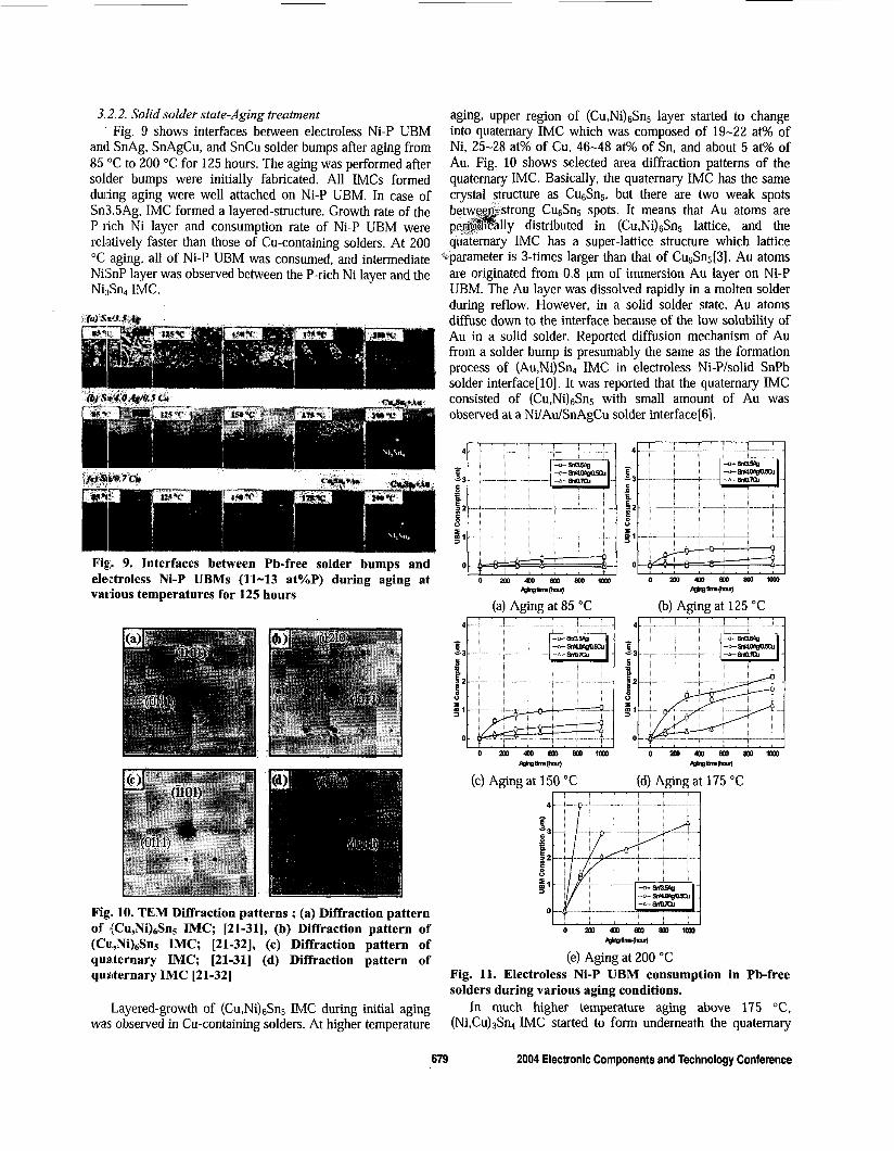
3.2.2, Solid solder state-Aging treatment Fig. 9 shows interfaces between electroless Ni-P UBM
and SnAg, SnAgCu, and SnCu solder bumps after aging from 85 "C to 200 "C for 125 hours. The aging was performed after solder bumps were initially fabricated. All IMCs formed during aging were well attached on Ni-P UBM. In case of Sn3.5Ag, IMC formed a layered-structure. Growth rate of the P-rich Ni layer and consumption rate of Ni-P UBM were relatively faster than those of Cu-containing solders. At 200 "C aging, all of Ni-P UBM was consumed, and intermediate NiSnP layer was observed between the P-rich Ni layer and the Ni:{Sn4 IMC.
Fig. 9. Interfaces between Pb-free solder bumps and electroless Ni-P UBMs (11-13 at%P) during aging at various temperatures for 125 hours
Fig. 10. TEM Diffraction patterns ; (a) Diffraction pattern of 1(Cu,Ni)&n5 IMC; [21-311, (b) Diffraction pattern of (Cui,Ni)&n5 IMC; [21-321, (c) Diffraction pattern of quadernary IMC; [21-311 (d) Diffraction pattern of quaternary IMC [21-321
Layered-growth of ( C ~ , N i ) ~ s n ~ IMC during initial aging was observed in Cu-containing solders. At higher temperature
aging, upper region of ( C u , N i ) & , layer started to change into quaternary IMC which was composed of 19-22 at% of Ni, 25-28 at% of Cu, 46-48 at% of Sn, and about 5 at% of Au. Fig. 10 shows selected area diffraction patterns of the quaternary IMC. Basically, the quaternary IMC has the same crystal structure as CuGSn5, but there are two weak spots
strong Cu6Sn5 spots. It means that Au atoms are lly distributed in (Cu,Ni)& lattice, and the
quaternary IMC has a super-lattice structure which lattice 'cparameter is 3-times larger than that of Cu6Sns[3]. Au atoms
are originated from 0.8 pm of immersion Au layer on Ni-P UBM. The Au layer was dissolved rapidly in a molten solder during reflow. However, in a solid solder state, Au atoms diffuse down to the interface because of the low solubility of Au in a solid solder. Reported diffusion mechanism of Au from a solder bump is presumably the same as the formation process of (Au,Ni)Sn4 IMC in electroless Ni-P/solid SnPb solder interface[lO]. It was reported that the quaternary IMC consisted of ( C ~ , N i ) ~ s n ~ with small amount of Au was observed at a Ni/Au/SnAgCu solder interfacet61.
WWhW aget4W-l
(a) Aging at 85 "C (b) Aging at 125 "C 4 -- - _ - - - - 4 - .__-__ - *
(c) Aging at 150 "C (d) Aging at 175 "C
o a m ~ ~ s o o l m mane0
(e) Aging at 200 "C Fig. 11. Electroless Ni-P UBM consumption in Pb-free solders during various aging conditions.
In much higher temperature aging above 175 "C, (Ni,Cu)& IMC started to form underneath the quaternary
679 2004 Electronic Components and Technology Conference

IMC. In solid solder state, ( N i , c ~ ) ~ S n ~ IMC grew as a layered-structure, and grain growth or spalling of (Cu,Ni) 6Sn5 IMC were not observed. Formation of (Ni,C~)~sn4 IMC was due to the reduced Cu diffusion from a bulk solder. In order to form ( N i , c ~ ) ~ S n ~ IMC at the interface between the P-rich PJi layer and the quaternary IMC, Sn atoms must diffuse through the quaternary IMC. Therefore, the growth rate of (Ni,Cu) 3Sn4 IMC will be determined by the Sn diffusion through the quaternary IMC.
Fig. 11 shows UBM consumption rates of Sn3.5Ag, Sn4.0Ag0.5Cu, and SnO.7Cu solder bumps during aging. Similar to a molten solder state, Sn3.5Ag showed much faster LJBM consumption rate than the other two Cu-containing solders. During ( c ~ , N i ) ~ S n ~ IMC formation at 85 and 125 "C, Sn4.0AgO.SCu and SnO.7Cu solders showed nearly the same ZJBM consumption rate. However, Sn0.7Cu showed slower IJBM consumption rate than Sn4.0Ag0.5Cu at high temperature such as 175 and 200 "C. Fig. 12 shows remaining LJBM thickness in Sn4.0Ag0.5Cu and Sn0.7Cu solder bumps after aging at 175 "C for 500 hrs and aging at 200 "C for 500 hrs. After aging at 175 "C for 500 hrs, layered-structure of two IMCs made of quaternary IMC and ( N i , c ~ ) ~ S n ~ IMC was observed in Sn4.0Ag0.5Cu solder bumps. However, in Sn0.7Cu solder bump, only ( C ~ , N i ) ~ s n ~ IMC was observed after the same heat treatment. After aging at 200 "C for 500 hrs, all UBM layer was consumed in Sn4.0Ag0.5Cu solder, but, nearly 3 pm of UBM layer still remained in Sn0.7Cu solder. It was observed that more (CU,N~)&~ IMC formed and less electroless Ni-P UBM consumed in higher Cu- containing solders during solid state reactions. After Cu depletion in solder bumps, ( N i , c ~ ) ~ S n ~ IMC started to form under (CU,Ni)& IMC because of continuous Sn diffusion through ( C U , N ~ ) ~ S ~ ~ IMC. At this stage, UBM consumption rate is determined by the diffusion rate of Sn through ( c ~ , N i ) ~ S n ~ layer.
175 .c Soohrs 200 *c JMhm 200 IC SOOh
Fig.12. Interface between electroless Ni UBM and (a) SnAgCu solder and (b) SnCu solder bumps
Based on these results, suitable Pb-free solder alloys for electroless Ni-P UBM can be suggested. Generally, Cu-added solder alloys such as Sn4.0AgO.SCu and Sn0.7Cu are better than Pb-free solder alloys without Cu in terms of lower UBM consumption rate. Especially, for high temperature applications, more Cu addition in solder alloy would be better for lowering consumption of electroless Ni-P UBMs.
3.3. Effects of solder alloy components on bump shearing behavior 3.3.1 Effect of Bi addition (5-6 at% P-containing Ni UBh')
Bump shear test was performed on SnAg and SnAgBi solder bumps after reflow at 260 C for lmin. Maximum shear strength of each solder was higher in case of SnAgBi than in case of SnAg (Fig. 13-(a), (d)). Shear force of SnAg was almost constant near the maximum force and decreased slowly. However, shear force of SnAgBi reached maximum force, and decreased rapidly. SnAg solder bumps 'were sheared inside solder bumps as shown in Fig. 13-(b), (c). However, SnAgBi solder bumps were sheared at the solder- IMC interface, as shown in Fig. 13- (e), (0.
Shear strength of SnAgBi solder bumps was higher than that of SnAg presumably due to a hardening effect of Bi precipitation.[4, 51 The fact implies that Bi improves :shear strength inside of solder bumps.
(4 (e) (10 Fig. 13. (a) Force vs. displacement curve, (b) shearing behavior, and (c) fractured site of Sn3.5Ag. (d) Force vs. displacement curve, (e) shearing behavior, and (f) fracture site of Sn3.5Ag4.8Bi.
3.3.2 Effect of Cu addition in solder alloy (11-13 ai% P- containing Ni UBM)
After reflow at various temperatures for 30 seconds, SnAg bumps showed the highest shear strength (-70 g.force), and SnCu bumps showed the lowest shear strength (-40 gforce). Bump shear strengths of SnAg, SnAgCu, and SnCu :;older bumps after aging were about 60, 60, and 40 g.force, respectively. Generally, bump shear strength of each solder bumps follow ultimate tensile strength of solder alloys[21].
Besides bump shear strength, bump shear force vs. displacement curves (Fig. 14) is also important. The area under the curve means bump toughness during a bump shear test. As the area under a curve becomes larger, deformation of solder bump becomes more plastic. In Fig. 14, SnAg .solder bump after reflowed at 260 "C for 30 seconds shows higher bump shear strength and shorter displacement, which represents a brittle fracture. The fractured surface of reflowed SnAg solder bumps occurred through the P-rich Ni la,yer as shown in Fig. 15. However, in case of other solders, sheared surfaces were inside solder bumps. Spailed Ni3Sn4 IRK of
680 2004 Electronic Components and Technology Conlerence
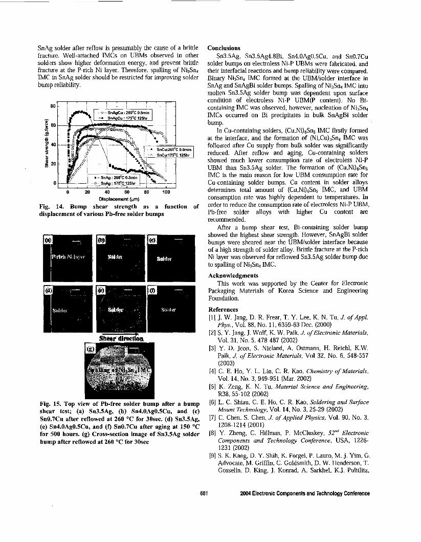
SnAg solder after reflow is presumably the cause of a brittle fracture. Well-attached IMCs on UBMs observed in other solders show higher deformation energy, and prevent brittle fracture at the P-rich Ni layer. Therefore, spalling of Ni3Sn4 IMC in SnAg solder should be restricted for improving solder bump reliability.
Conclusions Sn3.5Ag, Sn3.5Ag4.8Bi. Sn4.OAgO.EiCu, and SnO.7Cu
solder bumps on electroless Ni-P UBMs were fabricated, and their interfacial reactions and bump reliability were compared. Binary Ni3Sn4 IMC formed at the UBM/solder interface in SnAg and SnAgBi solder bumps. Spalling of Ni3Sn4 IMC into molten Sn3.5Ag solder bump was dependent upon surface condition of electroless Ni-P UBM(P content). No Bi-
0 20 40 60 80 100 Displacement (pm)
Fig. 14. Bump shear strength as a function of displacement of various Pb-free solder bumps
Fig. 15. Top view of Pb-free solder bump after a bump shear test; (a) Sn3.5Ag, (b) Snrl.OAgO.SCu, and (c) Sn0.7Cu after reflowed at 260 "C for 30sec. (d) Sn3.5Ag, (e) Sn4.OAg0.5Cu, and (f) Sn0.7Cu after aging at 150 "C for i500 hours. (g) Cross-section image of Sn3.5Ag solder bump after reflowed at 260 "C for 30sec
containing IMC was observed, however, nucleation of Ni3Sn4 IMCs occurred on Bi precipitates in bulk SnAgBi solder bump.
In Cu-containing solders, ( C ~ , N i ) ~ s n ~ IMC firstly formed at the interface, and the formation of ( N i , c ~ ) ~ S n ~ IMC was followed after Cu supply from bulk solder was significantly reduced. After reflow and aging, Cu-containing solders showed much lower consumption rate of electroless Ni-P UBM than Sn3.5Ag solder. The formation of (Cu,Ni)&n~ IMC is the main reason for low UBM consumption rate for Cu-containing solder bumps. Cu content in solder alloys determines total amount of (Cu,Ni)6SnS IMC, and UBM consumption rate was highly dependent to temperatures. In order to reduce the consumption rate of electroless Ni-P UBM, Pb-free solder alloys with higher Cu content are recommended.
After a bump shear test, Bi-containing solder bump showed the highest shear strength. However, SnAgBi solder bumps were sheared near the UBM/solder interface because of a high strength of solder alloy. Brittle fracture at the P-rich Ni layer was observed for reflowed Sn3.5Ag solder bump due to spalling of Ni3Sn4 IMC.
Acknowledgments This work was supported by the Center for Electronic
Packaging Materials of Korea Science and Engineering Foundation.
References [l] J. W. Jang, D. R. Frear, T. Y. Lee, K. N. Tu, J. ofAppl.
Phys., Vol. 88, No. 11, 6359-63 Dec. (2000) [2] S. Y. Jang, J. Wolf, K. W. Paik, J. ofElectronic Materials,
Vol. 31, No. 5, 478-487 (2002) [3] Y . D. Jeon, S. Nieland, A. Ostmann, H. Reichl, K.W.
Paik, J. of Electronic Materials, Vol 32, No. 6 , 548-557 (2003)
[4] C. E. Ho, Y. L. Lin, C. R. Kao, Chemistry of Materials, Vol. 14, No. 3,949-951 (Mar. 2002)
[5] K. Zeng, K. N. Tu, Material Science and Engineering,
[6] L. C. Shiau, C. E. Ho, C. R. Kao, Soldering and Surface
[7] C. Chen, S . Chen, J. ofApplied Physics, Vol. 90, No. 3,
[8] Y. Zheng, C. Hillman, P. McCluskey, 52"d Electronic Components and Technology Conference, USA, 1226- 1231 (2002)
[9] S. K. Kang, D. Y. Shih, K. Forgel, P. Lauro, M. J. Yim, G. Advocate, M. Griffin, C. Goldsmith, D. W. Henderson, T. Gosselin, D. King, J. Konrad, A. Sarkhel, K.J. Pulttlitz,
R38, 55-102 (2002)
Mount Technology, Vol. 14, No. 3, 25-29 (2002)
1208-1214 (2001)
681 2004 Electronic Components and Technology Conference

51" Electronic Components and Technology Conference, USA, 448-454 (2001)
[lo] K. Y . Lee, M. Li, D. R. Olsen, W. T. Chen, 51"' Electronic Components and Technology Conference, USA, 478-486 (2001)
[ l l ] K. Zeng, V. Vuorinen, J. K. Kivilahti, 5Z"' Electronic Components and Technology Conference, USA, 693-698
[12] Y . Chonan, T. Komiyama, Jin Onuki, R. Urao, Proc. of the 7'h Int. Symp., JWS, Kobe, 1311-1314 (2001)
[13] M. Nishiura, A. Nakayama, S . Sakatani, Y . Kohara, T. Saeki, K. Uenishi, K. F. Kobayashi, Proc. ofthe 7'h Int. Symp., JWS, Kobe, 1305-1310 (2001)
[14] D. R. Lide, CRC Handbook of Chemistry and Physics, CRC Press, Inc., 76* edition, 6-259 (1995)
[15] D. A. Porter, K. E. Easterling, Phase Transformations in Metals and Alloys, Chapman & Hall, UK, Znd edition, 60- 106 (1992)
I161 H. Wever, Defect and Diffusion Forum, Vol. 83, 55-72 (1992)
[ 171 Paul Shewmon, Diffusion in Solids, A Publication of the Minerals, Metals, & Materials Society, USA, 180-184 (1 989)
[18] B. F. Dyson, T. T. Anthony, D. Turnbull, J. Appl. Phys., 38,3408 (1967)
[19] M. Schaefer, R. A. Fournelle, J. Liang, J. of Electronic Materials, Vol. 27, No. 11, 1167-1176 (1998)
[20] P. L. Tu, Y . C. Chan, K. C. Hung, J. K. L. Lai, Scripta Mater., Vol. 44, 317-323 (2001)
[21] J. Madeni, S . Liu, and T. Siewei, "Casting of Lead-Free Solder Specimens with Various Solidification Rates", ASM- International Conference, Indianapolis (2001)
(2001)
aCOLOR 1
682
The CD-ROM version of this paper contains color, to assist you in interpretation.
2004 Electronic Components and Technology Conference


![1 Interfacial Rheology System. 2 Background of Interfacial Rheology Interfacial Shear Stress Interfacial Shear Viscosity = [ ]](https://static.fdocuments.net/doc/165x107/56649d1f5503460f949f3d29/1-interfacial-rheology-system-2-background-of-interfacial-rheology-interfacial.jpg)

