Interaction of metallic nanoparticles with dielectric substrates: effect of optical constants
9
Interaction of metallic nanoparticles with dielectric substrates: effect of optical constants This article has been downloaded from IOPscience. Please scroll down to see the full text article. 2013 Nanotechnology 24 035201 (http://iopscience.iop.org/0957-4484/24/3/035201) Download details: IP Address: 165.91.74.118 The article was downloaded on 20/03/2013 at 21:35 Please note that terms and conditions apply. View the table of contents for this issue, or go to the journal homepage for more Home Search Collections Journals About Contact us My IOPscience
Transcript of Interaction of metallic nanoparticles with dielectric substrates: effect of optical constants

Interaction of metallic nanoparticles with dielectric substrates: effect of optical constants
This article has been downloaded from IOPscience. Please scroll down to see the full text article.
2013 Nanotechnology 24 035201
(http://iopscience.iop.org/0957-4484/24/3/035201)
Download details:
IP Address: 165.91.74.118
The article was downloaded on 20/03/2013 at 21:35
Please note that terms and conditions apply.
View the table of contents for this issue, or go to the journal homepage for more
Home Search Collections Journals About Contact us My IOPscience
IOP PUBLISHING NANOTECHNOLOGY
Nanotechnology 24 (2013) 035201 (8pp) doi:10.1088/0957-4484/24/3/035201
Interaction of metallic nanoparticles withdielectric substrates: effect of opticalconstantsTanya Hutter1, Stephen R Elliott1 and Sumeet Mahajan2,3
1 Department of Chemistry, University of Cambridge, Cambridge CB2 1EW, UK2 Department of Physics, Cavendish Laboratory, University of Cambridge, CB3 0HE, UK
E-mail: [email protected]
Received 23 July 2012, in final form 14 November 2012Published 21 December 2012Online at stacks.iop.org/Nano/24/035201
AbstractIn this paper, we study the local-field enhancement in a system of a metallic nanoparticleplaced very near to a dielectric substrate. In such systems, intense electric fields are localizedin the gap between the particle and the substrate, creating a ‘hot-spot’ under appropriateexcitation conditions. We use finite-element numerical simulations in order to study the fieldenhancement in this dielectric–metal system. More specifically, we show how the opticalproperties of the dielectric substrate (n and k) affect the plasmonic field enhancement in thenano-gap. We also analyze the degree of field confinement in the gap and discuss it in thecontext of utilization for surface-enhanced Raman scattering. We finally show the fieldsgenerated by real substrates and compare them to metallic ones.
S Online supplementary data available from stacks.iop.org/Nano/24/035201/mmedia
(Some figures may appear in colour only in the online journal)
1. Introduction
Collective oscillations of electrons in metallic nanoparticlescoupled to incident light create highly localized fields,which have been widely studied in the field of plasmonics.These intense fields have found application in enhancingnear-field phenomena, including the highly popular techniqueof surface-enhanced Raman scattering (SERS) [1, 2]. A100-fold enhancement in the local field leads to a 100-milliontimes increase in the Raman signal in SERS owing to thequartic dependence on the electric field, E. Although themeasured enhancement factors in SERS are usually lowerthan those predicted, the remarkable sensitivity of SERS toE underlines the importance of understanding and designingappropriate plasmonic structures [3].
Single metallic nanoparticles (NPs) on a smooth metallicsurface can create high fields in the gap between the NPand the substrate [4]. The presence of the metallic substrate
3 Present Address: Institute of Life Sciences (IfLS), University ofSouthampton, SO17 1BJ, UK.
modifies the optical properties of the NP significantly. Theinteraction between the NP and the substrate results instrongly red-shifted plasmons as a result of hybridizationbetween the localized plasmon modes of the NP and thepropagating plasmon modes of the substrate [5, 6]. Thestrength of these modes is critically dependent on thegap distance and consequently affects the observed Ramanenhancement [7]. However, for a metallic NP near a dielectricsurface, there are no substrate surface-plasmon modes; onlythe localized surface-plasmon resonance (LSPR) mode of theindividual metallic nanoparticle interacts with the dielectricsubstrate. The interaction is akin to the well-established effectof a dielectric environment [8] although here it is asymmetric,being confined to one side of the NP. The charge oscillationsof the NP are screened by those induced in the substrate,resulting in localized hybridized NP plasmons [9, 10] confinedto the gap between them. The substrate has an influence on thenanoparticle spectrum due to the reduced symmetry inducedby the presence of the dielectric substrate. The effect is seenbetter on higher permittivity substrates compared to lowerpermittivity substrates such as silica glass [11]. Recently,
10957-4484/13/035201+08$33.00 c© 2013 IOP Publishing Ltd Printed in the UK & the USA

Nanotechnology 24 (2013) 035201 T Hutter et al
Spinelli et al published work on metal nanoparticles placedon top of a high-refractive-index substrate [12], where theystudied the effect of the real part of the refractive index of thesubstrate on the plasmonic resonances of silver nanoparticleswith different shapes. They showed that, for spherical NPs,both the dipolar and the quadrupolar resonances are almostunaffected by the presence of the substrate. However, this wasnot probed in depth; neither the near-field nor the effect of thecomplex refractive index of the substrate on enhancements inthe gap was studied.
This simulation-based study aims to understand theelectric field enhancement in a system consisting of aspherical metallic NP on a dielectric substrate, separated bya nano-sized gap. More specifically, the goal is to understandhow the real and imaginary parts of the refractive indexof a dielectric material affect the field enhancement in thenano-gaps. In our study, we find that the plasmon modes areaffected by the optical constants of the substrate as a resultof its interaction with the spherical nanoparticle. We alsoconsider the degree of field confinement in the gap, whichis important for localized SERS measurements. In addition,the effects of geometrical features, such as the size of theNP and the gap height, are investigated. In contrast to studiesthat focus on the extinction (the far-field), we focus on thenear-field and the enhancement in the gap, in the SERScontext. These aspects can be vital for utilization of near-fieldphenomena, including plasmon-enhanced photovoltaics andin situ spectroscopy on dielectric surfaces.
2. Numerical simulations
A two-dimensional model using COMSOL Multiphysicsv4.3, a commercial finite-element mode solver, was con-structed to enable parametric studies. The simulationswere performed in two steps. The first step computes theelectric field for the substrate only when illuminated witha p-polarized plane wave excitation at the upper boundary,E0,x = E0 · exp(i · k0 · y), where E0 = 1 V m−1, propagatingin the (−y) direction. The left and right side borders weredefined as perfect electric conductors (PECs) and the lowerborder satisfied the scattering boundary condition. This stepgives the electric field taking into account the presence ofthe substrate and is necessary to get the input field that theNP actually experiences. The second step was solved for thefield due to the presence of the NP on the substrate using theoutput from the first step. Perfectly matched layers (PMLs)were used to absorb the scattered radiation in all directions(in order to eliminate reflection back to the model); theirthickness was 100 nm. A schematic illustration of the twosteps of the model can be found in figure 1. The total widthand height of the model were 1200 nm, and the substratewas 300 nm thick. The model was solved for wavelengthsbetween 300 and 1000 nm, with a step size of 2 nm. Thedielectric substrate was modeled using frequency-independentrefractive-index values. The optical constants of the materialswere taken from [13]. A sufficiently small mesh (0.2 nm) wasused at the gap and at the surface of the particle comparedto the bulk of the model, where the maximum mesh size was
Figure 1. (a) The first computational step solved for the substrateonly with the excitation field at normal incidence propagating in the(−y) direction and polarization in the x direction. (b) The secondcomputational step computes the field due to the presence of theparticle above the substrate. The scattered field is then absorbed bythe surrounding PMLs to eliminate reflections.
set to 20 nm for the air domain and 12 nm for the substrate.The field was calculated as a ratio of its value with the NPat a given point to the incident field, |E|/|E0|. The results forthe near-field discussed in this work are spectral plots of themaximum values of |E|/|E0| found along a horizontal linein the middle of the gap. It is to be noted that the SERSenhancement factor is dependent on the fourth power of thefield.
3. Results and discussion
3.1. Effect of the gap distance between a silver NP and adielectric substrate
Local electric fields are of great importance to SERS andnear-field microscopy. In the gap between the NP and thesubstrate, a region of high electromagnetic field, the so-called‘hot-spot’, is generated. The gap can be created by a molecularspacer layer [7] or a transparent dielectric layer [14] andthus can be manipulated. Hence, we studied the effect ofthe gap distance on the near-field behavior in the gapbetween the nanoparticle and the dielectric surface. We useda non-dispersive and non-absorbing dielectric substrate (n =2, k = 0) and a silver nanoparticle (with radius R = 25 nm)under normal incidence with p-polarized light.
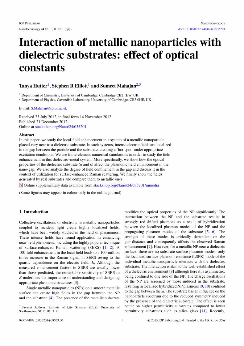
The presence of the substrate significantly affects thenear-field around the metallic particle and we compare asingle Ag NP in air with one that is placed 2 nm above adielectric substrate. In figures 2(a) and (b) the spatial electricfield distribution is shown for the two cases at a wavelength of354 nm. For the single NP in air, the dipole mode shows higherelectric fields at both sides of the NP due to charge separationinside the NP. However, when placed above a substrate, thesmaller the gap, the stronger the interaction between the NPand the substrate, and the charge distribution in the metallicNP shifts towards the bottom of the particle, resulting in asmaller dipolar charge separation in the NP. Thus the fielddistribution in the gap shows two lobes with high intensity anda dip in the middle under the NP. The electric field decreasesslightly when moving away from the NP’s surface towardsthe substrate. The position of maximum electric field is not
2
Nanotechnology 24 (2013) 035201 T Hutter et al
Figure 2. The electric field distribution of an Ag NP withR = 25 nm (a) in air and (b) 2 nm above a dielectric substrate(n = 2, k = 0) at 354 nm. (c) Plot of the maximum electric field|E|/|E0| spectra in the gap for different gap distances between theNP and the dielectric substrate. Inset: The maximum electric field isplotted as a function of the gap distance; the highest enhancementoccurs at a slightly different wavelength for each gap distance.Rectangles—electric field in the middle of the gap, circles—electricfield 0.3 nm below the NP.
constant in space and it will change with the strength of theinteraction between the NP and the dielectric surface. Hence,in this study we use the highest electric field along a horizontalline in the middle of the gap, as it will be a more appropriateindicator of the strength of the interaction between the NP andthe dielectric substrate, rather than using the field at a fixedpoint.
The gap distance between the nanoparticle and thesubstrate is crucial for determining the interaction betweenthem. We varied the gap from 0.6 to 20 nm to see itseffect on the near-field for the case of a silver NP ona smooth dielectric substrate. The maximum electric field|E|/|E0| along a horizontal line in the middle of the gap isplotted in figure 2(c). The inset shows the dependence ofthe highest electric field in the gap on the gap distance. Weplot the maximum electric field along a horizontal line in themiddle of the gap (rectangles) and, to account for the factthat the distance changes as the gap increases, we also plotthe maximum electric field along a horizontal line 0.3 nmbelow the NP (circles). The values 0.3 nm below the NPare slightly higher compared to the ones in the middle ofthe gap, as expected. This is because in the former case,the electric field is probed at a further distance from theNP as the gap increases. Nevertheless, in both cases, theelectric field increases as the gap decreases due to strongerinteraction of the NP with the substrate. We note that the|E|/|E0| values are obtained at a wavelength correspondingto the peak in the enhancement curve (figure 2(c)) and not ata fixed wavelength.
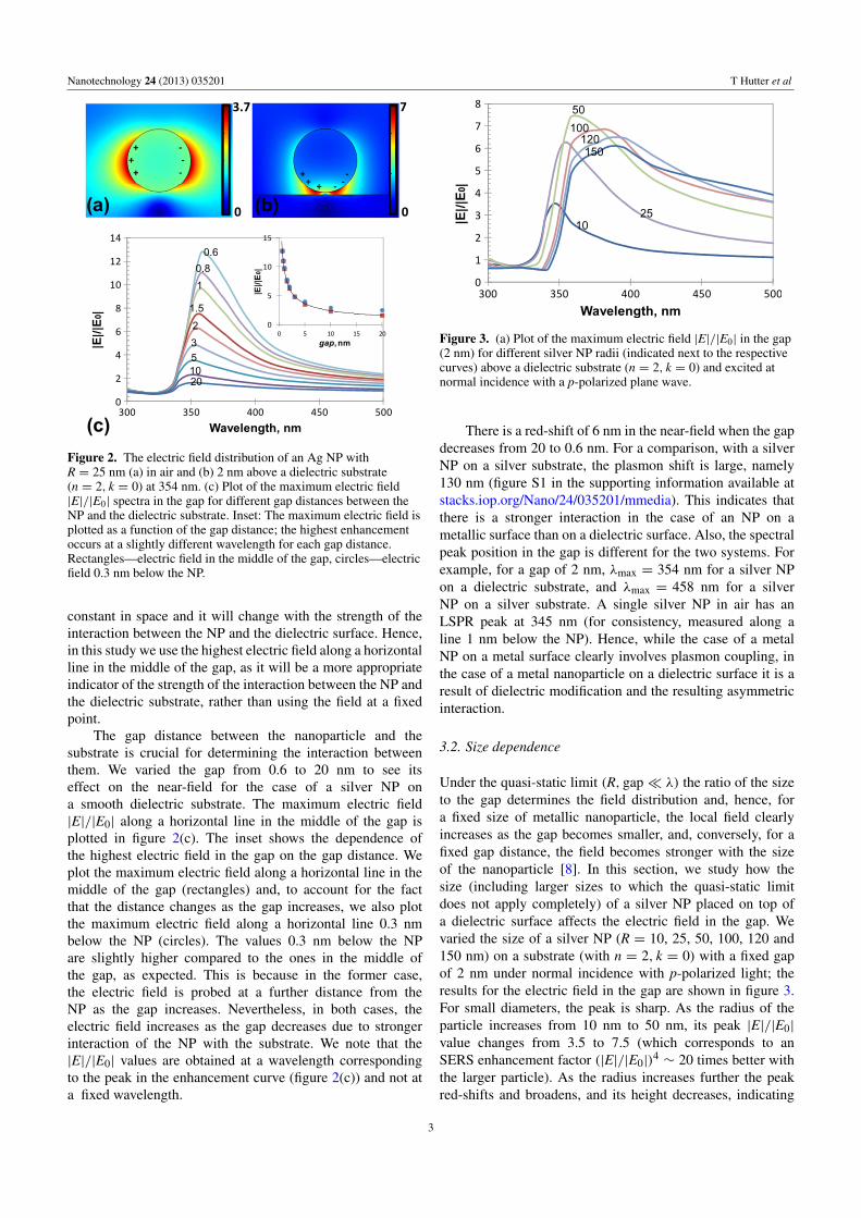
Figure 3. (a) Plot of the maximum electric field |E|/|E0| in the gap(2 nm) for different silver NP radii (indicated next to the respectivecurves) above a dielectric substrate (n = 2, k = 0) and excited atnormal incidence with a p-polarized plane wave.
There is a red-shift of 6 nm in the near-field when the gapdecreases from 20 to 0.6 nm. For a comparison, with a silverNP on a silver substrate, the plasmon shift is large, namely130 nm (figure S1 in the supporting information available atstacks.iop.org/Nano/24/035201/mmedia). This indicates thatthere is a stronger interaction in the case of an NP on ametallic surface than on a dielectric surface. Also, the spectralpeak position in the gap is different for the two systems. Forexample, for a gap of 2 nm, λmax = 354 nm for a silver NPon a dielectric substrate, and λmax = 458 nm for a silverNP on a silver substrate. A single silver NP in air has anLSPR peak at 345 nm (for consistency, measured along aline 1 nm below the NP). Hence, while the case of a metalNP on a metal surface clearly involves plasmon coupling, inthe case of a metal nanoparticle on a dielectric surface it is aresult of dielectric modification and the resulting asymmetricinteraction.
3.2. Size dependence
Under the quasi-static limit (R, gap� λ) the ratio of the sizeto the gap determines the field distribution and, hence, fora fixed size of metallic nanoparticle, the local field clearlyincreases as the gap becomes smaller, and, conversely, for afixed gap distance, the field becomes stronger with the sizeof the nanoparticle [8]. In this section, we study how thesize (including larger sizes to which the quasi-static limitdoes not apply completely) of a silver NP placed on top ofa dielectric surface affects the electric field in the gap. Wevaried the size of a silver NP (R = 10, 25, 50, 100, 120 and150 nm) on a substrate (with n = 2, k = 0) with a fixed gapof 2 nm under normal incidence with p-polarized light; theresults for the electric field in the gap are shown in figure 3.For small diameters, the peak is sharp. As the radius of theparticle increases from 10 nm to 50 nm, its peak |E|/|E0|
value changes from 3.5 to 7.5 (which corresponds to anSERS enhancement factor (|E|/|E0|)
4∼ 20 times better with
the larger particle). As the radius increases further the peakred-shifts and broadens, and its height decreases, indicating
3
Nanotechnology 24 (2013) 035201 T Hutter et al
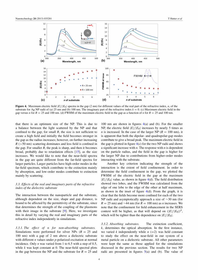
Figure 4. Maximum electric field |E|/|E0| spectra in the gap (2 nm) for different values of the real part of the refractive index, n, of thesubstrate for Ag NP radii of (a) 25 nm and (b) 100 nm. The imaginary part of the refractive index k = 0. (c) Maximum electric field in thegap versus n for R = 25 and 100 nm. (d) FWHM of the maximum electric field in the gap as a function of n for R = 25 and 100 nm.
that there is an optimum size of the NP. This is due toa balance between the light scattered by the NP and thatconfined to the gap; for small R, the size is not sufficient tocreate a high field and initially the field becomes stronger inthe gap as the radius increases; however, on further increasingR (>50 nm) scattering dominates and less field is confined inthe gap. For smaller R, the peak is sharp, and then it becomesbroad, probably due to retardation effects [15], as the sizeincreases. We would like to note that the near-field spectrain the gap are quite different from the far-field spectra forlarger particles. Larger particles have high-order modes in thefar-field spectrum, which contribute to the extinction mainlyby absorption, and low-order modes contribute to extinctionmainly by scattering.
3.3. Effects of the real and imaginary parts of the refractiveindex of the dielectric substrate
The interaction between the nanoparticle and the substrate,although dependent on the size, shape and gap distance, isbound to be affected by the permittivity of the substrate, sincethat determines the strength of the coupling of the plasmonswith their image in the substrate [9]. Here, we investigatethis in detail by varying the real and imaginary parts of therefractive index independently in simulations.
3.3.1. The effect of n for non-absorbing substrates.Simulations were performed for silver NPs (R = 25 and100 nm) with a gap of 2 nm above a dielectric substratewith different n values under p-polarized excitation at normalincidence. Only n was varied from 1 to 6.5 with a step of 0.5,while k was kept constant at 0. The near-field spectral plotsin the gap between the NP and the substrate for R = 25 and
100 nm are shown in figures 4(a) and (b). For the smallerNP, the electric field |E|/|E0| increases by nearly 5 times asn is increased. In the case of the larger NP (R = 100 nm), itis apparent that both the dipolar- and quadrupolar-gap modescontribute to give a broad peak. The maximum electric field inthe gap is plotted in figure 4(c) for the two NP radii and showsa significant increase with n. The response with n is dependenton the particle radius, and the field in the gap is higher forthe larger NP due to contributions from higher-order modesinteracting with the substrate.
Another key criterion indicating the strength of theinteraction is the extent of field confinement. In order todetermine the field confinement in the gap, we plotted theFWHM of the electric field in the gap at the maximum|E|/|E0| value, as shown in figure 4(d). The field distributionshowed two lobes, and the FWHM was calculated from theedge of one lobe to the edge of the other at half maximum,as shown in the inset of figure 4(d). From the graph, it isclear that the fields become more confined for each of the twoNP radii and asymptotically approach a size of ∼30 nm (forR = 25 nm) and∼44 nm (for R = 100 nm) as n increases. Wenote that the confinement for field enhancement in the SERScontext will be higher, as that will depend on (|E|/|E0|)
4,which will be tighter than the dependence on |E|/|E0|.
3.3.2. Absorbing substrates. The extinction coefficient,k, determines the optical absorption. In the first instance,we varied k independently while n (=2) was held constantto study the effect on the near-field in our system of ametal particle on a dielectric substrate. All other parameterswere kept the same as those applied for the simulationsdiscussed in the previous section. The results for two NPradii are presented in figures 5(a) and (b). The value of
4
Nanotechnology 24 (2013) 035201 T Hutter et al
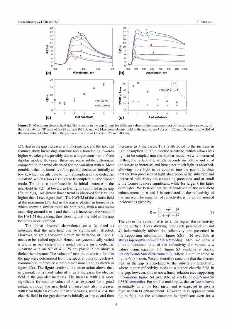
Figure 5. Maximum electric field |E|/|E0| spectra in the gap (2 nm) for different values of the imaginary part of the refractive index, k, ofthe substrate for NP radii of (a) 25 nm and (b) 100 nm. (c) Maximum electric field in the gap versus k for R = 25 and 100 nm. (d) FWHM ofthe maximum electric field in the gap as a function of k for R = 25 and 100 nm.
|E|/|E0| in the gap increases with increasing k and the spectralfeatures show increasing structure and a broadening towardshigher wavelengths, possibly due to a larger contribution fromdipolar modes. However, there are some subtle differencescompared to the trend observed for the variation with n. Mostnotable is that the intensity of the peak(s) decreases initially atlow k, which we attribute to light absorption in the dielectricsubstrate, which allows less light to be coupled into the dipolarmode. This is also manifested in the initial decrease in thenear-field |E|/|E0| at lower k as less light is confined in the gap(figure 5(c)). An almost linear trend is observed for k valueshigher than 1 (see figure 5(c)). The FWHM of the electric fieldat the maximum |E|/|E0| in the gap is plotted in figure 5(d),which shows a similar trend for both radii, with a maximumoccurring around k = 1 and then, as k increases, the value ofthe FWHM decreasing, thus showing that the field in the gapbecomes more confined.
The above observed dependence on k (at fixed n)indicates that the near-field can be significantly affected.However, to get a complete picture the variation of n and kneeds to be studied together. Hence, we systematically variedn and k in our system of a metal particle on a dielectricsubstrate with an NP of R = 25 nm placed 2 nm above adielectric substrate. The values of maximum electric field inthe gap were determined from the spectral plots for each n–kcombination to produce a three-dimensional plot, as shown infigure 6(a). The figure confirms the observation above that,in general, for a fixed value of n, as k increases the electricfield in the gap also increases. The increase with k is moresignificant for smaller values of n, as expected for a goodmetal, although the near-field enhancement also increaseswith k for higher n values. For fixed n values, when n < 4, theelectric field in the gap decreases initially at low k, and then
increases as k increases. This is attributed to the increase inlight absorption in the dielectric substrate, which allows lesslight to be coupled into the dipolar mode. As k is increasedfurther, the reflectivity, which depends on both n and k, ofthe substrate increases and hence not much light is absorbed,allowing more light to be coupled into the gap. It is clearthat the two processes of light absorption in the substrate andincreased reflectivity are competing processes, and at smallk the former is more significant, while for larger k the latterdominates. We believe that the dependence of the near-fieldenhancement on n and k is correlated to the reflectivity ofthe surface. The equation of reflectivity, R, in air for normalincidence is given by
R =(1− n)2 + k2
(1+ n)2 + k2 . (1)
The closer the value of R is to 1, the higher the reflectivityof the surface. Plots showing how each parameter (n andk) independently affects the reflectivity are presented inthe supporting information (figure S2(a), (b) available atstacks.iop.org/Nano/24/035201/mmedia). Also, we show athree-dimensional plot of the reflectivity for various n–kvalues using equation (1) (figure S3 available at stacks.iop.org/Nano/24/035201/mmedia), where a similar trend tofigure 6(a) is seen. We can therefore conclude that the electricfield in the gap is correlated to the substrate’s reflectivity,where higher reflectivity leads to a higher electric field inthe gap; however, this is not a linear relation (see supportinginformation figure S4 available at stacks.iop.org/Nano/24/035201/mmedia). For small n and large k, the surface behavesessentially as a low loss metal and is expected to give ahigh near-field enhancement. However, it is apparent fromfigure 6(a) that the enhancement is significant even for a
5
Nanotechnology 24 (2013) 035201 T Hutter et al
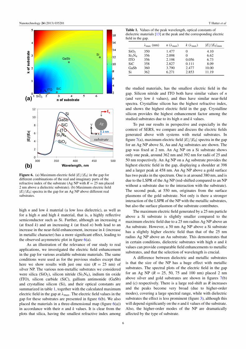
Figure 6. (a) Maximum electric field |E|/|E0| in the gap fordifferent combinations of the real and imaginary parts of therefractive index of the substrate (Ag NP with R = 25 nm placed2 nm above a dielectric substrate). (b) Maximum electric field|E|/|E0| spectra in the gap for an Ag NP above different realsubstrates.
high n and low k material (a low loss dielectric), as well asfor a high n and high k material, that is, a highly reflectivesemiconductor such as Si. Further, although an increasing n(at fixed k) and an increasing k (at fixed n) both lead to anincrease in the near-field enhancement, increase in k (increasein metallic character) has a more significant effect, leading tothe observed asymmetric plot in figure 6(a).
As an illustration of the relevance of our study to realapplications, we investigated the electric field enhancementin the gap for various available substrate materials. The sameconditions were used as for the previous studies except thathere we show results with just one size (R = 25 nm) ofsilver NP. The various non-metallic substrates we consideredwere silica (SiO2), silicon nitride (Si3N4), indium tin oxide(ITO), silicon carbide (SiC), gallium antimonide (GaSb)and crystalline silicon (Si), and their optical constants aresummarized in table 1, together with the calculated maximumelectric field in the gap at λmax. The electric field values in thegap for these substrates are presented in figure 6(b). We alsoplaced the materials in a three-dimensional map (figure 6(a))in accordance with their n and k values. It is clear from theplots that silica, having the smallest refractive index among
Table 1. Values of the peak wavelength, optical constants ofdielectric materials [13] at the peak and the corresponding electricfield in the gap.
λmax (nm) n (λmax) k (λmax) |E|/|E0|max
SiO2 350 1.477 0 4.10Si3N4 356 2.098 0 6.62ITO 356 2.198 0.056 6.73SiC 358 2.827 0.111 8.09GaSb 360 3.790 2.477 10.00Si 362 6.271 2.853 11.19
the studied materials, has the smallest electric field in thegap. Silicon nitride and ITO both have similar values of n(and very low k values), and thus have similar near-fieldspectra. Crystalline silicon has the highest refractive index,and shows the highest electric field in the gap. Crystallinesilicon provides the highest enhancement factor among thestudied substrates due to its high n and k values.
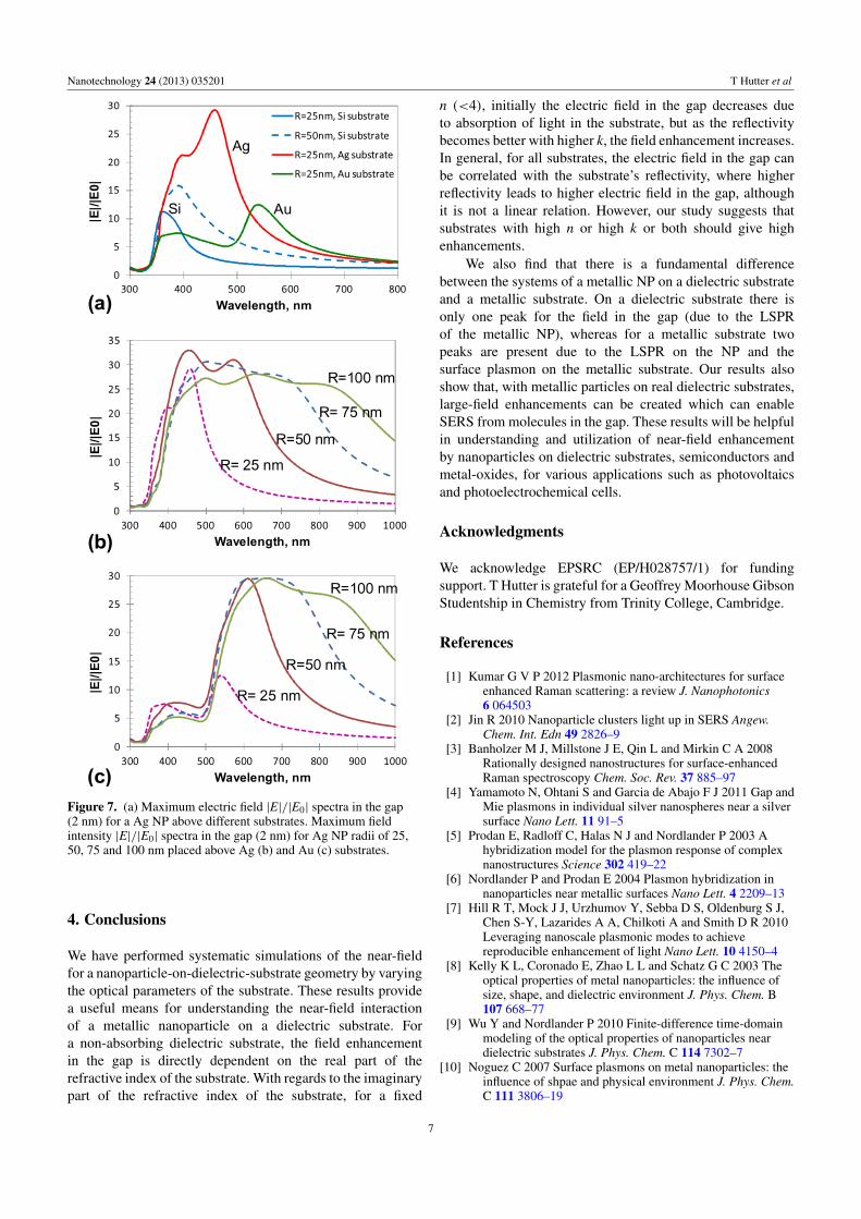
To put our results in perspective and especially in thecontext of SERS, we compare and discuss the electric fieldsgenerated above with systems with metal substrates. Infigure 7(a), maximum electric field |E|/|E0| spectra in the gapfor an Ag NP above Si, Au and Ag substrates are shown. Thegap was fixed at 2 nm. An Ag NP on a Si substrate showsonly one peak, around 362 nm and 392 nm for radii of 25 and50 nm respectively. An Ag NP on a Ag substrate provides thehighest electric field in the gap, displaying a shoulder at 398and a larger peak at 458 nm. An Ag NP above a gold surfacehas two peaks in the spectrum. One is at around 380 nm, and isdue to the LSPR of the Ag NP (red-shifted compared to an NPwithout a substrate due to the interaction with the substrate).The second peak, at 550 nm, originates from the surfaceplasmons of the gold substrate. Not only is there a strongerinteraction of the LSPR of the NP with the metallic substrates,but also the surface plasmon of the substrate contributes.
The maximum electric field generated by a 25 nm particleabove a Si substrate is slightly smaller compared to themaximum electric field due to a 25 nm radius Ag NP above anAu substrate. However, a 50 nm Ag NP above a Si substratehas a slightly higher electric field than that of the 25 nmradius Ag NP above an Au substrate. This demonstrates thatin certain conditions, dielectric substrates with high n and kvalues can provide comparable field enhancements to metallicsubstrates, and that the selection of wavelength is crucial.
A difference between dielectric and metallic substratesis that the size of the NP has a huge effect with metallicsubstrates. The spectral plots of the electric field in the gapfor an Ag NP (R = 25, 50, 75 and 100 nm) placed 2 nmabove silver and gold substrates are shown in figures 7(b)and (c) respectively. There is a large red-shift as R increasesand the peaks become very broad (due to higher-ordermodes), covering a large spectral range, while with dielectricsubstrates the effect is less prominent (figure 3), although thiswill depend significantly on the n and k values of the substrate.Also, the higher-order modes of the NP are dramaticallyaffected by the type of substrate.
6
Nanotechnology 24 (2013) 035201 T Hutter et al
Figure 7. (a) Maximum electric field |E|/|E0| spectra in the gap(2 nm) for a Ag NP above different substrates. Maximum fieldintensity |E|/|E0| spectra in the gap (2 nm) for Ag NP radii of 25,50, 75 and 100 nm placed above Ag (b) and Au (c) substrates.
4. Conclusions
We have performed systematic simulations of the near-fieldfor a nanoparticle-on-dielectric-substrate geometry by varyingthe optical parameters of the substrate. These results providea useful means for understanding the near-field interactionof a metallic nanoparticle on a dielectric substrate. Fora non-absorbing dielectric substrate, the field enhancementin the gap is directly dependent on the real part of therefractive index of the substrate. With regards to the imaginarypart of the refractive index of the substrate, for a fixed
n (<4), initially the electric field in the gap decreases dueto absorption of light in the substrate, but as the reflectivitybecomes better with higher k, the field enhancement increases.In general, for all substrates, the electric field in the gap canbe correlated with the substrate’s reflectivity, where higherreflectivity leads to higher electric field in the gap, althoughit is not a linear relation. However, our study suggests thatsubstrates with high n or high k or both should give highenhancements.
We also find that there is a fundamental differencebetween the systems of a metallic NP on a dielectric substrateand a metallic substrate. On a dielectric substrate there isonly one peak for the field in the gap (due to the LSPRof the metallic NP), whereas for a metallic substrate twopeaks are present due to the LSPR on the NP and thesurface plasmon on the metallic substrate. Our results alsoshow that, with metallic particles on real dielectric substrates,large-field enhancements can be created which can enableSERS from molecules in the gap. These results will be helpfulin understanding and utilization of near-field enhancementby nanoparticles on dielectric substrates, semiconductors andmetal-oxides, for various applications such as photovoltaicsand photoelectrochemical cells.
Acknowledgments
We acknowledge EPSRC (EP/H028757/1) for fundingsupport. T Hutter is grateful for a Geoffrey Moorhouse GibsonStudentship in Chemistry from Trinity College, Cambridge.
References
[1] Kumar G V P 2012 Plasmonic nano-architectures for surfaceenhanced Raman scattering: a review J. Nanophotonics6 064503
[2] Jin R 2010 Nanoparticle clusters light up in SERS Angew.Chem. Int. Edn 49 2826–9
[3] Banholzer M J, Millstone J E, Qin L and Mirkin C A 2008Rationally designed nanostructures for surface-enhancedRaman spectroscopy Chem. Soc. Rev. 37 885–97
[4] Yamamoto N, Ohtani S and Garcia de Abajo F J 2011 Gap andMie plasmons in individual silver nanospheres near a silversurface Nano Lett. 11 91–5
[5] Prodan E, Radloff C, Halas N J and Nordlander P 2003 Ahybridization model for the plasmon response of complexnanostructures Science 302 419–22
[6] Nordlander P and Prodan E 2004 Plasmon hybridization innanoparticles near metallic surfaces Nano Lett. 4 2209–13
[7] Hill R T, Mock J J, Urzhumov Y, Sebba D S, Oldenburg S J,Chen S-Y, Lazarides A A, Chilkoti A and Smith D R 2010Leveraging nanoscale plasmonic modes to achievereproducible enhancement of light Nano Lett. 10 4150–4
[8] Kelly K L, Coronado E, Zhao L L and Schatz G C 2003 Theoptical properties of metal nanoparticles: the influence ofsize, shape, and dielectric environment J. Phys. Chem. B107 668–77
[9] Wu Y and Nordlander P 2010 Finite-difference time-domainmodeling of the optical properties of nanoparticles neardielectric substrates J. Phys. Chem. C 114 7302–7
[10] Noguez C 2007 Surface plasmons on metal nanoparticles: theinfluence of shpae and physical environment J. Phys. Chem.C 111 3806–19
7
Nanotechnology 24 (2013) 035201 T Hutter et al
[11] Knight M W, Wu Y, Lassiter J B, Nordlander P andHalas N J 2009 Substrates matter: influence of an adjacentdielectric on an individual plasmonic nanoparticle NanoLett. 9 2188–92
[12] Spinelli P, van Lare C, Verhagen E and Polman A 2011Controlling Fano lineshapes in plasmon-mediated lightcoupling into a substrate Opt. Express 19 A303–11
[13] Ni X, Liu Z and Kildishev A V 2010 PhotonicsDB: opticalconstants http://nanohub.org/resources/PhotonicsDB
[14] Mubeen S, Zhang S, Kim N, Lee S, Kraemer S, Xu H andMoskovits M 2012 Plasmonic properties of goldnanoparticles separated from a gold mirror by an ultrathinoxide Nano Lett. 12 2088–94
[15] Myroshnychenko V, Rodriguez-Fernandez J,Pastoriza-Santos I, Funston A M, Novo C, Mulvaney P,Liz-Marzan L M and Garcia de Abajo F J 2008 Modellingthe optical response of gold nanoparticles Chem. Soc. Rev.37 1792–805
8