Intel Desktop Board BP810 - tcshavasu.com
92
Intel ® Desktop Board BP810 Technical Product Specification The Desktop Board BP810 may contain design defects or errors known as errata that may cause the product to deviate from published specifications. Current characterized errata are documented in the Desktop Board BP810 Specification Update. September 1999 Order Number 751306-001
Transcript of Intel Desktop Board BP810 - tcshavasu.com

Intel® Desktop Board BP810Technical Product Specification
The Desktop Board BP810 may contain design defects or errors known as errata that may cause the product to deviate from published specifications. Current characterized errataare documented in the Desktop Board BP810 Specification Update.
September 1999
Order Number 751306-001

Revision History
Revision Revision History Date
-001 First Release of the Intel® BP810 Desktop Board Technical ProductSpecification
October 1999
This product specification applies to only standard BP810 boards with BIOS identifierBP81010A.86A.
Changes to this specification will be published in the Desktop Board BP810 Specification Updatebefore being incorporated into a revision of this document.
Information in this document is provided in connection with Intel® products. No license, express or implied, by estoppel orotherwise, to any intellectual property rights is granted by this document. Except as provided in Intel’s Terms and Conditionsof Sale for such products, Intel assumes no liability whatsoever, and Intel disclaims any express or implied warranty, relatingto sale and/or use of Intel products including liability or warranties relating to fitness for a particular purpose, merchantability,or infringement of any patent, copyright or other intellectual property right. Intel products are not intended for use in medical,life saving, or life sustaining applications.
Intel may make changes to specifications and product descriptions at any time, without notice.
The BP810 desktop board may contain design defects or errors known as errata that may cause the product to deviate frompublished specifications. Current characterized errata are available on request.
Contact your local Intel sales office or your distributor to obtain the latest specifications before placing your product order.
Copies of documents which have an ordering number and are referenced in this document, or other Intel literature, may beobtained from:
Intel CorporationP.O. Box 5937Denver, CO 80217-9808
or call in North America 1-800-548-4725, Europe 44-0-1793-431-155, France 44-0-1793-421-777,Germany 44-0-1793-421-333, other Countries 708-296-9333.
† Third-party brands and names are the property of their respective owners.
Copyright 1999, Intel Corporation. All rights reserved.
iii
Preface
This Technical Product Specification (TPS) specifies the board layout, components, connectors,power and environmental requirements, and the BIOS for the BP810 board. It describes thestandard BP810 board product and available manufacturing options.
Intended AudienceThe TPS is intended to provide detailed, technical information about the board and its componentsto the vendors, system integrators, and other engineers and technicians who need this level ofinformation. It is specifically not intended for general audiences.
What This Document ContainsChapter Description
1 A description of the hardware used on this board
2 A map of the resources of the board
3 The features supported by the BIOS Setup program
4 The contents of the BIOS Setup program’s menus and submenus
5 A description of the BIOS error messages, beep codes, and POST codes
Typographical ConventionsThis section contains information about the conventions used in this specification. Not all of thesesymbols and abbreviations appear in all specifications of this type.
Notes, Cautions, and Warnings
NOTE
Notes call attention to important information.
CAUTIONCautions are included to help you avoid damaging hardware or losing data.
WARNINGWarnings indicate conditions which, if not observed, can cause personal injury.

Intel Desktop Board BP810 Technical Product Specification
iv
Other Common Notation# Used after a signal name to identify an active-low signal (such as USBP0#).
(NxnX) When used in the description of a component, N indicates component type, xn are the relativecoordinates of its location on the board, and X is the instance of the particular part at that generallocation. For example, J5J1 is a connector, located at 5J. It is the first connector in the 5J area.
KB Kilobyte (1024 bytes)
Kbit Kilobit (1024 bits)
MB Megabyte (1,048,576 bytes)
Mbit Megabit (1,048,576 bits)
GB Gigabyte (1,073,741,824 bytes)
xxh An address or data value ending with a lowercase h indicates a hexadecimal value.
x.x V Volts. Voltages are DC unless otherwise specified.† This symbol is used to indicate third-party brands and names that are the property of their
respective owners.

v
Contents
1 Board Description1.1 Overview ................................................................................................................... 12
1.1.1 Feature Summary........................................................................................ 121.1.2 Manufacturing Options ................................................................................ 131.1.3 Board Layout............................................................................................... 141.1.4 Block Diagram............................................................................................. 15
1.2 Online Support........................................................................................................... 161.3 Design Specifications ................................................................................................ 161.4 Processor .................................................................................................................. 181.5 System Memory......................................................................................................... 191.6 Intel® 810 Chipset...................................................................................................... 20
1.6.1 AGP ............................................................................................................ 211.6.2 USB............................................................................................................. 211.6.3 IDE Support................................................................................................. 221.6.4 Real-Time Clock, CMOS SRAM, and Battery .............................................. 22
1.7 I/O Controller ............................................................................................................. 231.8 Serial Port.................................................................................................................. 231.9 Graphics Subsystem.................................................................................................. 241.10 Audio Subsystem....................................................................................................... 25
1.10.1 AD1881 Analog Codec................................................................................ 251.10.2 Audio Connectors........................................................................................ 26
1.11 Hardware Management Features .............................................................................. 261.12 Networking Subsystem (Optional).............................................................................. 27
1.12.1 10BASE-T Ethernet Interface Features ....................................................... 271.12.2 HomePNA Interface Features...................................................................... 271.12.3 Power Management and Power Saving Features........................................ 27
1.13 Modem Subsystem.................................................................................................... 281.13.1 Software Modem ......................................................................................... 281.13.2 Modem Codec............................................................................................. 281.13.3 Modem AT Commands and S-Register Settings ......................................... 281.13.4 Modem Specifications ................................................................................. 29
1.14 Power Management Features.................................................................................... 301.14.1 ACPI............................................................................................................ 301.14.2 Hardware Support ....................................................................................... 32
2 Technical Reference2.1 Introduction................................................................................................................ 372.2 Memory Map.............................................................................................................. 372.3 I/O Map...................................................................................................................... 382.4 DMA Channels .......................................................................................................... 392.5 PCI Configuration Space Map ................................................................................... 402.6 Interrupts ................................................................................................................... 402.7 PCI Interrupt Routing Map ......................................................................................... 41

Intel Desktop Board BP810 Technical Product Specification
vi
2.8 Connectors ................................................................................................................ 422.8.1 Back Panel Connectors ............................................................................... 432.8.2 Midboard Connectors .................................................................................. 462.8.3 Front Panel Connector ................................................................................ 50
2.9 Jumper Block............................................................................................................. 532.10 Mechanical Considerations........................................................................................ 55
2.10.1 FlexATX Form Factor .................................................................................. 552.10.2 I/O Shield .................................................................................................... 56
2.11 Electrical Considerations ........................................................................................... 572.11.1 Power Consumption .................................................................................... 572.11.2 Power Supply Considerations...................................................................... 572.11.3 Standby Current Requirements ................................................................... 582.11.4 Fan Power Requirements............................................................................ 58
2.12 Thermal Considerations............................................................................................. 592.13 Reliability ................................................................................................................... 602.14 Environmental............................................................................................................ 612.15 Regulatory Compliance ............................................................................................. 61
2.15.1 Safety Regulations ...................................................................................... 612.15.2 EMC Regulations ........................................................................................ 622.15.3 Telecommunications Regulations................................................................ 622.15.4 Certification Markings.................................................................................. 63
3 Overview of BIOS Features3.1 Introduction................................................................................................................ 653.2 BIOS Flash Memory Organization ............................................................................. 663.3 Resource Configuration ............................................................................................. 67
3.3.1 PCI Autoconfiguration.................................................................................. 673.3.2 PCI IDE Support.......................................................................................... 67
3.4 System Management BIOS (SMBIOS) ...................................................................... 683.5 BIOS Upgrades ......................................................................................................... 69
3.5.1 Language Support....................................................................................... 693.5.2 Custom Splash Screen................................................................................ 69
3.6 Recovering BIOS Data .............................................................................................. 703.7 Boot Options.............................................................................................................. 71
3.7.1 Booting from CD-ROM ................................................................................ 713.7.2 Booting Without Attached Devices .............................................................. 71
3.8 USB Legacy Support ................................................................................................. 723.9 BIOS Security Features ............................................................................................. 73
4 BIOS Setup Program4.1 Introduction................................................................................................................ 754.2 Maintenance Menu .................................................................................................... 764.3 Main Menu................................................................................................................. 77

Contents
vii
4.4 Advanced Menu......................................................................................................... 774.4.1 Boot Configuration Submenu....................................................................... 784.4.2 Peripheral Configuration Submenu.............................................................. 784.4.3 IDE Configuration ........................................................................................ 794.4.4 IDE Configuration Submenus ...................................................................... 804.4.5 Diskette Configurations Submenu ............................................................... 814.4.6 Event Log Configuration .............................................................................. 81
4.5 Security Menu............................................................................................................ 824.6 Boot Menu ................................................................................................................. 834.7 Exit Menu .................................................................................................................. 84
5 Error Messages and Beep Codes5.1 BIOS Error Messages................................................................................................ 855.2 Bus Initialization Checkpoints .................................................................................... 875.3 Speaker ..................................................................................................................... 885.4 BIOS Beep Codes ..................................................................................................... 895.5 Enhanced Diagnostic LEDs (Optional)....................................................................... 90
Figures1. Board Components ........................................................................................................... 142. Block Diagram................................................................................................................... 153. Intel 810 Chipset Block Diagram ....................................................................................... 204. Block Diagram of Audio Subsystem with AD1881 Codec .................................................. 255. Location of Standby Power Indicator LED ......................................................................... 346. Connector Groups............................................................................................................. 427. Back Panel Connectors..................................................................................................... 438. Midboard Connectors........................................................................................................ 469. Front Panel Connector ...................................................................................................... 5010. Location of the Jumper Block ............................................................................................ 5311. Board Dimensions............................................................................................................. 5512. I/O Shield Dimensions (without LAN Connector) ............................................................... 5613. Thermally-sensitive Components ...................................................................................... 5914. Memory Map of the Flash Memory Device ........................................................................ 6615. Enhanced Diagnostics LEDs............................................................................................. 90

Intel Desktop Board BP810 Technical Product Specification
viii
Tables1. Feature Summary ............................................................................................................. 122. Manufacturing Options ...................................................................................................... 133. Specifications.................................................................................................................... 164. Processors Supported by the Board.................................................................................. 185. System Memory Configuration .......................................................................................... 196. Supported Graphics Refresh Rates................................................................................... 247. Modem Specifications ....................................................................................................... 298. Effects of Pressing the Power Switch ................................................................................ 309. Power States and Targeted System Power ....................................................................... 3110. Wake Up Devices and Events ........................................................................................... 3211. Fan Connector Descriptions.............................................................................................. 3312. System Memory Map ........................................................................................................ 3713. I/O Map ........................................................................................................................... 3814. DMA Channels .................................................................................................................. 3915. PCI Configuration Space Map........................................................................................... 4016. Interrupts .......................................................................................................................... 4017. PCI Interrupt Routing Map................................................................................................. 4118. USB Connectors ............................................................................................................... 4419. VGA Port Connector ......................................................................................................... 4420. LAN Connector (Optional) ................................................................................................. 4421. Audio Line Out Connector ................................................................................................. 4522. Mic In Connector ............................................................................................................... 4523. Telephone Jack................................................................................................................. 4524. Processor Fan Connector (J5J1)....................................................................................... 4725. Front Panel USB (J7G1) ................................................................................................... 4726. Power Connector (J7G3)................................................................................................... 4727. Diskette Drive Connector (J7D1)....................................................................................... 4828. Serial Port Connector (J7B2)............................................................................................. 4829. IDE Connector (J7B1) ....................................................................................................... 4930. Chassis Fan Connector (J3A2) ......................................................................................... 4931. Front Panel Connector (J7G2) .......................................................................................... 5132. States for a Single-colored Power LED ............................................................................. 5133. States for a Dual-colored Power LED................................................................................ 5134. BIOS Setup Configuration Jumper Settings (J5A1) ........................................................... 5435. Power Usage .................................................................................................................... 5736. Standby Current Usage..................................................................................................... 5837. Chassis Fan (J3A2) DC Power Requirements................................................................... 5838. Thermal Considerations for Components .......................................................................... 6039. Board Environmental Specifications .................................................................................. 6140. Safety Regulations ............................................................................................................ 6141. EMC Regulations .............................................................................................................. 6242. Telecommunications Regulations...................................................................................... 6243. Supervisor and User Password Functions......................................................................... 7344. BIOS Setup Program Menu Bar ........................................................................................ 7545. BIOS Setup Program Function Keys ................................................................................. 7646. Maintenance Menu............................................................................................................ 7647. Main Menu ....................................................................................................................... 7748. Advanced Menu ................................................................................................................ 77

Contents
ix
49. Boot Configuration Submenu ............................................................................................ 7850. Peripheral Configuration Submenu.................................................................................... 7851. IDE Device Configuration .................................................................................................. 7952. IDE Configuration Submenus............................................................................................ 8053. Diskette Configurations Submenu ..................................................................................... 8154. Event Log Configuration Submenu.................................................................................... 8155. Security Menu ................................................................................................................... 8256. Boot Menu ........................................................................................................................ 8357. Exit Menu ........................................................................................................................ 8458. BIOS Error Messages ....................................................................................................... 8559. Bus Initialization Checkpoints............................................................................................ 8760. Upper Nibble High Byte Functions .................................................................................... 8761. Lower Nibble High Byte Functions .................................................................................... 8862. Beep Codes ..................................................................................................................... 8963. Enhanced Diagnostics Codes ........................................................................................... 91

Intel Desktop Board BP810 Technical Product Specification
x

11
1 Board Description
What This Chapter Contains1.1 Overview ................................................................................................................... 121.2 Online Support........................................................................................................... 161.3 Design Specifications ................................................................................................ 161.4 Processor .................................................................................................................. 181.5 System Memory......................................................................................................... 191.6 Intel® 810 Chipset...................................................................................................... 201.7 I/O Controller ............................................................................................................. 231.8 Serial Port.................................................................................................................. 231.9 Graphics Subsystem.................................................................................................. 241.10 Audio Subsystem....................................................................................................... 251.11 Hardware Management Features .............................................................................. 261.12 Networking Subsystem (Optional).............................................................................. 271.13 Modem Subsystem.................................................................................................... 281.14 Power Management Features.................................................................................... 30

Intel Desktop Board BP810 Technical Product Specification
12
1.1 Overview
1.1.1 Feature SummaryTable 1 summarizes the BP810 board’s major features.
Table 1. Feature Summary
Form Factor FlexATX (9.0 inches by 7.2 inches)
Processor Support for an Intel® Celeron™ processor in a PPGA package
Memory • One 168-pin dual inline memory module (DIMM) socket
• Supports up to 256 MB of 100 MHz non-ECC synchronous DRAM (SDRAM)
• Support for serial presence detect (SPD) and non-SPD DIMMs
Chipset Intel® 810 Chipset, consisting of:
• Intel® 82810 Graphics/Memory Controller Hub (GMCH) (See Table 2, on page 13for information on manufacturing options)
• Intel® 82801 I/O Controller Hub (ICH) (See Table 2, on page 13 for information onmanufacturing options)
• Intel® 82802AB 4 Mbit Firmware Hub (FWH)
AcceleratedGraphics Port(AGP) Video
• Intel® 82810 GMCH graphics support (See Table 2, on page 13 for information onmanufacturing options)
Audio Audio Codec ’97 (AC’97) compatible audio subsystem, consisting of the following:
• Intel 82801AA ICH (AC link output)
• Analog Devices AD1881 analog codec
I/O Control IT8761E Low Pin Count (LPC) I/O controller
Onboard modem • Motorola SM56 AC-L (AC link) software modem
• Silicon Laboratories Si3038 family MC ’97 modem codec
PeripheralInterfaces
• Four universal serial bus (USB) ports
• One IDE interface with Ultra DMA support
• One diskette drive interface
• One 9-pin serial port connector
BIOS • Intel/AMI BIOS stored in an Intel 82802AB 4 Mbit firmware hub (FWH)
• Support for Advanced Configuration and Power Interface (ACPI), Plug and Play,and SMBIOS
NOTE
The BP810 board is designed to support only USB-aware operating systems.
For information about Refer to
The board’s compliance level with ACPI, Plug and Play, and SMBIOS Section 1.3, page 16

Board Description
13
1.1.2 Manufacturing OptionsTable 2 describes the BP810 board’s manufacturing options. Not every manufacturing option isavailable in all marketing channels. Please contact your Intel representative to determine whichmanufacturing options are available to you.
Table 2. Manufacturing Options
AGP Video One of the following two options:
• Intel 82810 GMCH DC-100 with 4 MB display cache
• Intel 8210 GMCH0 with no display cache
I/O Controller Hub(ICH)
One of the following two options:
• Intel 82801AA ICH1 with support for ATA-66 devices, Suspend-to-RAM, and Wakefrom USB
• Intel 82801AB ICH0 with support for ATA-33 devices
Networkingsubsystem
Intel® 21145 Phoneline/Ethernet LAN controller, providing:
• 10 Mb/s 10BASE-T networking
• 1 Mb/s HomePNA port
Hardware MonitorSubsystem
• Hardware monitor component
• Temperature sense
• Voltage sense to detect out of range values
Enhanceddiagnostics
• Four dual-color LEDs on back panel
Instantly availablePC
• Support for PCI Local Bus Specification, Revision 2.2
• Suspend-to-RAM support
• Wake from USB

Intel Desktop Board BP810 Technical Product Specification
14
1.1.3 Board Layout
Figure 1 shows the location of the major components on the board.
OM08677
A
O
L
J
M
K
N
P
C
B
ED
I GH F
A Back panel connectors I SpeakerB Intel 82810 GMCH J IDE connectorC Processor socket K Intel 82801I/O Controller Hub (ICH)D Battery L IT8761E I/O controllerE DIMM socket M Intel 82802AB Firmware Hub (FWH)F Front panel connector N Intel 21145 Integrated Phoneline/Ethernet Controller (optional)G Power connector O AD1881 analog codecH Diskette drive connector P 4 MB display cache (optional)
Figure 1. Board Components

Board Description
15
1.1.4 Block DiagramFigure 2 is a block diagram of the major functional areas of the board.
810 Chipset
ProcessorSocket
DIMMSocket
Primary IDE
LPC I/OController
USBBus
66 MHzHost Bus
AC LinkAnalogCodec
HardwareMonitor
(Optional)
82801 I/O Controller Hub(ICH)
82810Graphics Memory
Controller Hub(GMCH)
82802ABFirmware Hub
(FWH)
100 MHzSDRAM
Bus
AHABus
DisplayInterface
VGAPort
4 MB DisplayCache
(Optional)
OM08865
DiagnosticLEDs
(Optional)
Line Out
Mic In
Port 4
Port 3USBHub
Controller
LPCBus
DisketteDrive
Connector
Port 2
Port 1
IntegratedPhoneline/Ethernet
Controller(Optional)
ModemCodec
SMBus
SMI Bus
PCI BusRJ-11PhoneLine
Serial PortConnector
Low-PassFilter
RJ-45Connector 1 Mb/s
HomePNAPort
10 Mb/sEthernet
Figure 2. Block Diagram

Intel Desktop Board BP810 Technical Product Specification
16
1.2 Online SupportFind information about Intel desktop boards under “Product Info” or “Customer Support” at theseWorld Wide Web sites:
http://www.intel.com/design/motherbdhttp://support.intel.com/support/motherboards/desktop
1.3 Design SpecificationsTable 3 lists the specifications applicable to the BP810 board.
Table 3. Specifications
Specification Description Revision Level
AC ‘97 Audio Codec ‘97 Revision 2.1, May 1998, Intel Corporation. The specification isavailable at:
ftp://download.intel.com/pc-supp/platform/ac97
ACPI AdvancedConfiguration andPower Interfacespecification
Revision 1.0, July 1, 1998, Intel Corporation, MicrosoftCorporation, and Toshiba Corporation. The specification isavailable at:
http://www.teleport.com/~acpi/
AGP Accelerated GraphicsPort InterfaceSpecification(2X only)
Revision 2.0, May 4, 1998, Intel Corporation.The specification is available through theAccelerated Graphics Implementers Forum at:
http://www.agpforum.org/
AMI BIOS American Megatrends AMIBIOS 98, American Megatrends, Inc.The specification is available at:
http://www.amibios.com
ATA-3 Information Technology- AT Attachment-3Interface
X3T10/2008D Revision 6.The specification is available at:ATA Anonymous FTP Site: fission.dt.wdc.com
ATAPI ATA Packet Interfacefor CD-ROMs
SFF-8020i Revision 2.5.The specification is available at:(SFF) Fax Access: (408) 741-1600
ATX ATX Specification Revision 2.01, February 1997, Intel Corporation.The specification is available at:
http://developer.intel.com/design/motherbd.atx.htm
El Torito Bootable CD-ROMformat specification
Version 1.0, January 25, 1995, Phoenix Technologies Ltd. andIBM Corporation. The El Torito specification is available onthe Phoenix Web site at:
http://www.ptltd.com/techs/specs.html
FlexATX FlexATX addendum FlexATX Addendum Version 1.0 to the microATX Specification1.0, Intel Corporation. This specification is available at:
http://www.teleport.com/~ffsupprt/spec/FlexATXaddn1_01.pdf
continued

Board Description
17
Table 3. Specifications (continued)
Specification Description Revision Level
LPC Low Pin Count InterfaceSpecification
Revision 1.0, September 29, 1997, Intel Corporation.This specification is available at:
http://www.intel.com/design/chipsets/industry/lpc.htm
MicroATX microATX MotherboardInterface SpecificationSFX Power Supply DesignGuide
Version 1.0, December 1997, Intel Corporation.Version 1.0, December 1997, Intel Corporation.
PCI PCI Local Bus Specification Revision 2.2, December 18, 1998, PCI SpecialInterest Group. The specification is available at:
http://www.pcisig.com/
PCI PCI Bus Power ManagementInterface Specification
Revision 1.1, December 18, 1998, PCI SpecialInterest Group. The specification is available at:
http://www.pcisig.com/
Plug and Play Plug and Play BIOSspecification
Version 1.0a, May 5, 1994,Compaq Computer Corporation, PhoenixTechnologies Ltd., and Intel Corporation.
The specification is available at:
http://irving.co.intel.com/ntcdarchive/docs/wcd00006/wcd00615.htm
SDRAM DIMMs(64-and 72-bit)
PC SDRAM Unbuffered DIMMspecificationPC SDRAM DIMM SpecificationPC Serial Presence Detect(SPD) Specification
Revision 1.0, February 1998, Intel Corporation.Revision 1.5, November 1997, Intel Corporation.Revision 1.2A, December 1997, Intel Corporation.These specifications are available at:
http://www.intel.com/design/chipsets/memory/
SMBIOS System Management BIOS Version 2.3, 12 August 1998,Award Software International Inc., Dell ComputerCorporation, Hewlett-Packard Company,Intel Corporation, International Business MachinesCorporation, Phoenix Technologies Limited,American Megatrends Inc., and SystemSoftCorporation.
The specification is available at:
http://developer.intel.com/ial/wfm/design/smbios
UHCI Universal Host ControllerInterface
Design Guide Revision 1.1, March 1996,Intel Corporation. The design guide is available at:
http://www.usb.org/developers
USB Universal serial busspecification
Revision 1.1, September 23, 1998,Compaq Computer Corporation, Digital EquipmentCorporation, IBM PC Company, Intel Corporation,Microsoft Corporation, NEC, and Northern Telecom.
This specification is available at:
http://usb.org/developers
WfM Wired for Management Baseline Version 2.0, December 18, 1998, Intel Corporation.This specification is available at:
http://developer.intel.com/ial/WfM/wfmspecs.htm

Intel Desktop Board BP810 Technical Product Specification
18
1.4 Processor
CAUTIONThe BP810 board supports processors that draw a maximum of 15.2 A. Using a processor thatdraws more than 15.2 A can damage the processor, the board, and the power supply. See theprocessor’s data sheet for current usage requirements.
The board supports a single Celeron processor as shown in Table 4. The host bus speed isautomatically selected.
Table 4. Processors Supported by the Board
Processor Type Processor Speed Host Bus Frequency L2 Cache Size
Celeron processor 300A MHz333 MHz366 MHz400 MHz433 MHz466 MHz500 MHz
66 MHz66 MHz66 MHz66 MHz66 MHz66 MHz66 MHz
128 KB128 KB128 KB128 KB128 KB128 KB128 KB
All supported onboard memory can be cached, up to the cachability limit of the processor.
For information about Refer to
Processor support for the BP810 board http://support.intel.com/support/motherboards/desktop
Processor data sheets http://www.intel.com/design/litcentr

Board Description
19
1.5 System Memory
CAUTIONTo be fully compliant with all applicable Intel® SDRAM memory specifications, the board shouldbe populated with DIMMs that support the Serial Presence Detect (SPD) data structure. If yourmemory modules do not support SPD, you will see a notification to this effect on the screen atpower up. The BIOS will attempt to configure the memory controller for normal operation;however, DIMMs may not function at the determined frequency.
CAUTIONBecause the main system memory is also used as video memory, the BP810 requires 100 MHzSDRAM DIMMs even though the processor front side bus is 66 MHz. It is highly recommendedthat SPD DIMMs be used, since this allows the chipset to accurately configure memory settings foroptimum performance. If non-SPD memory is installed, the BIOS will attempt to correctlyconfigure the memory settings, but performance and reliability may be impacted
The board has one DIMM socket. The minimum memory size is 32 MB and the maximummemory size is 256 MB. The BIOS automatically detects memory type, size, and speed.
The board supports the following memory features:
• 3.3 V, 168-pin DIMMs with gold-plated contacts• 100 MHz SDRAM• Serial Presence Detect (SPD) or non-SPD memory• Non-ECC (64-bit) memory• Unbuffered single- or double-sided DIMMs
The board is designed to support DIMMs in the configurations listed in Table 5 below.
Table 5. System Memory Configuration
DIMM Size Non-ECC Configuration
32 MB 4 Mbit x 64
64 MB 8 Mbit x 64
128 MB 16 Mbit x 64
256 MB 32 Mbit x 64
For information about Refer to
The PC Serial Presence Detect Specification Table 3, page 16
Obtaining copies of PC SDRAM specifications http://www.intel.com/design/pcisets/memory

Intel Desktop Board BP810 Technical Product Specification
20
1.6 Intel® 810 ChipsetThe Intel 810 chipset consists of the following devices:
• Graphics Memory Controller Hub (GMCH) with accelerated hub architecture (AHA) bus. Theboard includes one of the following:
82810 GMCH DC-100 with 4 MB display cache
82810 GMCH0 with no display cache• I/O Controller Hub (ICH) with AHA bus. The board includes one of the following:
82801AA ICH1 with support for ATA-66 devices, Suspend-to-RAM, and Wake from USB
82801AB ICH0 with support for ATA-33 devices• 82802AB Firmware Hub (FWH)
The chipset provides the host, memory, AGP, and I/O interfaces shown in Figure 3.
810 Chipset
82801 I/O Controller Hub(ICH)
82810Graphics Memory
Controller Hub(GMCH)
82802ABFirmware Hub
(FWH)
100 MHzSDRAM
Bus
AHABus
IDE USBHost Bus
AC Link
PCI Bus
SMBus
LPC Bus
DisplayInterface
OM09031
Figure 3. Intel 810 Chipset Block Diagram
For information about Refer to
The Intel 810 chipset http://www.developer.intel.com
The resources used by the chipset Chapter 2
The chipset’s compliance with ACPI and AC ‘97 Table 3, page 16

Board Description
21
1.6.1 AGPThe integrated AGP is a high-performance bus for graphics-intensive applications, such as 3Dapplications. AGP, while based on the PCI Local Bus Specification, Rev. 2.1, is independent of thePCI bus and is intended for exclusive use with graphical display devices. AGP overcomes certainlimitations of the PCI bus related to handling large amount of graphics data with the followingfeatures:
• Pipelined memory read and write operations that hide memory access latency• Demultiplexing of address and data on the bus for nearly 100 percent bus efficiency
For information about Refer to
The location of the VGA port connector Figure 7, page 43
Obtaining the Accelerated Graphics Port Interface Specification Table 3, page 16
1.6.2 USBThe board has an onboard USB hub and four USB ports; one USB peripheral can be connected toeach port. For more than four USB devices, an external hub can be connected to any of the ports.Two of the USB ports are implemented with stacked back panel connectors. The other two arerouted to the front panel connector; accessing these ports requires a cable from the panel connectorto the front of the chassis. The board fully supports UHCI and uses UHCI-compatible softwaredrivers. USB features include:
• Self-identifying peripherals that can be plugged in while the computer is running• Automatic mapping of function to driver and configuration• Support for isochronous and asynchronous transfer types over the same set of wires• Support for up to 127 physical devices• Guaranteed bandwidth and low latencies appropriate for telephony, audio, and other
applications• Error-handling and fault-recovery mechanisms built into the protocol
NOTE
Computer systems that have an unshielded cable attached to a USB port may not meet FCCClass B requirements, even if no device or a low-speed USB device is attached to the cable. Useshielded cable that meets the requirements for full-speed devices.
For information about Refer to
The location of the USB connectors on the back panel Figure 7, page 43
The signal names of the USB connectors Table 18, page 44
The location of the front panel USB connector Figure 8, page 46
The signal names of the front panel USB connector Table 25, page 47
The USB and UHCI specifications Table 3, page 16

Intel Desktop Board BP810 Technical Product Specification
22
1.6.3 IDE SupportThe board has one bus-mastering IDE interface. This interface supports:
• ATAPI devices (such as CD-ROM drives)• ATA devices using the transfer modes listed in Table 52 on page 80
The BIOS supports logical block addressing (LBA) and extended cylinder head sector (ECHS)translation modes. The drive reports the transfer rate and translation mode to the BIOS.
The board supports laser servo (LS-120) diskette technology through its IDE interfaces. TheLS-120 drive can be configured as a boot device by setting the BIOS Setup program’s Boot menuto one of the following:
• ARMD-FDD (ATAPI removable media device – floppy disk drive)• ARMD-HDD (ATAPI removable media device – hard disk drive)
For information about Refer to
The location of the IDE connector Figure 8, page 46
The signal names of the IDE connector Table 29, page 49
BIOS Setup program’s Boot menu Table 56, page 83
1.6.4 Real-Time Clock, CMOS SRAM, and BatteryThe real-time clock is compatible with DS1287 and MC146818 components. The clock provides atime-of-day clock and a multicentury calendar with alarm features and century rollover. The real-time clock supports 256 bytes of battery-backed CMOS SRAM in two banks that are reserved forBIOS use.
A coin-cell battery powers the real-time clock and CMOS memory. When the computer is notplugged into a wall socket, the battery has an estimated life of three years. When the computer isplugged in, the 3.3 V standby current from the power supply extends the life of the battery. Theclock is accurate to ± 13 minutes/year at 25 ºC with 3.3 VSB applied.
The time, date, and CMOS values can be specified in the BIOS Setup program. The CMOS valuescan be returned to their defaults by using the BIOS Setup program.
NOTE
If the battery and AC power fail, standard defaults, not custom defaults, will be loaded into CMOSRAM at power on.

Board Description
23
NOTEThe recommended method of accessing the date in systems with Intel® desktop boards is indirectlyfrom the Real-Time Clock (RTC) via the BIOS. The BIOS on Intel desktop boards contains acentury checking and maintenance feature. This feature checks the two least significant digits ofthe year stored in the RTC during each BIOS request (INT 1Ah) to read the date and, if less than 80(i.e., 1980 is the first year supported by the PC), updates the century byte to 20. This featureenables operating systems and applications using the BIOS date/time services to reliablymanipulate the year as a four-digit value.
For information about Refer to
Proper date access in systems with Intel desktop boards http://support.intel.com/support/year2000/
1.7 I/O ControllerThe IT8761E I/O controller provides the following features:
• Low pin count (LPC) interface• One serial port• Plug and Play compatible register set• Support for SERIRQ protocol• Supports system management interrupt (SMI)• Interface for one 1.2 MB, 1.44 MB, or 2.88 MB diskette drive• Fan control and monitoring
The BIOS Setup program provides configuration options for the I/O controller.
For information about Refer to
The IT8761E I/O controller http://www.iteusa.com
1.8 Serial PortThe board has one 9-pin serial port connector. The serial port’s NS16C550-compatible UARTsupports data transfers at speeds up to 115.2 Kbits/sec with BIOS support. The serial port can beassigned as COM1 (3F8h), COM2 (2F8h), COM3 (3E8h), or COM4 (2E8h).
For information about Refer to
The location of the serial port connector Figure 8, page 46
The signal names of the serial port connector Table 28, page 48

Intel Desktop Board BP810 Technical Product Specification
24
1.9 Graphics SubsystemThe graphics subsystem provides the following features:
• Intel 82810 GMCH DC-100 graphics support, including:
Integrated 2D and 3D graphics engines
Integrated hardware motion compression engine
Integrated 230 MHz DAC• 4 MB of SDRAM display cache
A manufacturing option of this board replaces the GMCH component with the GMCH0 andremoves the 4 MB SDRAM display cache.
Table 6 lists the refresh rates supported by the graphics subsystem.
Table 6. Supported Graphics Refresh Rates
Resolution Available Refresh Rates (Hz)
640 x 200 x 16 colors 70
640 x 350 x 16 colors 70
640 x 400 x 256 colors 60, 70, 75, 85
640 x 400 x 64 K colors 60, 70, 75, 85
640 x 400 x 16 M colors 70
640 x 480 x 16 colors 60, 72, 75, 85
640 x 480 x 256 colors 60, 70, 72, 75, 85
640 x 480 x 32 K colors 60, 75, 85
640 x 480 x 64 K colors 60, 70, 72, 75, 85
640 x 480 x 16 M colors 60, 70, 72, 75, 85
800 x 600 x 256 colors 60, 75, 85
800 x 600 x 32 K colors 60, 70, 72, 75, 85
800 x 600 x 64 K colors 60, 70, 72, 75, 85
800 x 600 x 16 M colors 60, 70, 72, 75, 85
1024 x 768 x 256 colors 60, 70, 75, 85
1024 x 768 x 32 K colors 60, 75, 85
1024 x 768 x 64 K colors 60, 70, 72, 75, 85
1024 x 768 x 16 M colors 60, 70, 72, 75, 85
1056 x 800 x 16 colors 70
1280 x 1024 x 256 colors 60, 70, 72, 75, 85
1280 x 1024 x 32 K colors 60, 75, 85
1280 x 1024 x 64 K colors 60, 70, 72, 75
1280 x 1024 x 16 M colors 60, 70, 72, 75, 85
For information about Refer to
Obtaining graphics software and utilities http://support.intel.com/support/motherboards/desktop

Board Description
25
1.10 Audio SubsystemThe board includes an Audio Codec ’97 (AC ’97) compatible SoundMAX† audio subsystemconsisting of the these devices:
• Intel 82801 ICH (AC link output)• Analog Devices AD1881 analog codec
Figure 4 is a block diagram of the audio subsystem.
82801I/O Controller Hub (ICH)
AC LinkAD1881AnalogCodec Mic In
Line Out
OM09032
Figure 4. Block Diagram of Audio Subsystem with AD1881 Codec
Features of the audio subsystem include:
• Independent channels for PCM in, PCM out, and Mic in• 16-bit stereo I/O up to 48 kHz• Multiple sample rates
For information about Refer to
Obtaining audio software and utilities http://support.intel.com/support/motherboards/desktop
1.10.1 AD1881 Analog CodecThe AD1881 is a fully AC ’97 compliant codec. The codec's features include:
• 16-bit stereo full-duplex codec• CD-quality audio• Stereo line level output• Power management support• Full duplex variable sampling rate (7 kHz to 48 kHz) with 1 Hz resolution• Phat† Stereo 3D stereo enhancement
For information about Refer to
The audio subsystem’s compliance with AC ‘97 Table 3, page 16

Intel Desktop Board BP810 Technical Product Specification
26
1.10.2 Audio ConnectorsThe audio connectors, located on the back panel, include the following:
• Line out• Mic in
NOTE
CD-ROM digital audio signals are routed through the IDE interface.
For information about Refer to
The location of the back panel audio connectors Figure 7, page 43
The signal names of the back panel audio connectors Section 2.8.1, page 43
1.11 Hardware Management FeaturesThe hardware management features enable the board to be compatible with the Wired forManagement (WfM) specification. The board has several hardware management features,including the following:
• Hardware monitor component• Fan control and monitoring (implemented on the IT8761E I/O controller)
The optional hardware monitor component provides low-cost instrumentation capabilities. Thefeatures of the component include:
• Internal ambient temperature sensing• Remote thermal diode sensing for direct monitoring of processor temperature• Power supply monitoring (+12, +5, +3.3, +3.3 VSB, +2.5, VCCP) to detect levels above or
below acceptable values• SMBus interface
For information about Refer to
The WfM specification Table 3, page 16

Board Description
27
1.12 Networking Subsystem (Optional)The onboard networking subsystem consists of the following:
• Intel® 21145 Phoneline/Ethernet LAN controller• RJ-45 connector for 10 Mb/s 10BASE-T networking• RJ-11 connector for a 1 Mb/s HomePNA port
The Intel 21145 is an integrated Ethernet/HomePNA LAN controller for Ethernet networking thatintegrates a HomePNA physical layer interface for home networking on existing residential voice-grade telephone lines. The 10BASE-T port provides a direct 10 Mb/s Ethernet connection to atwisted pair interface. The HomePNA port provides a direct interface at a rate of 1 MB/s. TheHomePNA port shares the RJ-11 connector with the optional onboard modem. The Intel 21145supports autodetection between the 10BASE-T and HomePNA ports.
1.12.1 10BASE-T Ethernet Interface FeaturesThe 10BASE-T Ethernet Interface includes the following:
• Supports full-duplex operation• Provides internal and external loopback capability on all network ports• Supports IEEE 802.3 and ANSI 8802-3 Ethernet standards
1.12.2 HomePNA Interface FeaturesThe HomePNA Interface includes the following:
• Allows simultaneous phoneline networking and dial-up voice or internet access• Provides automatic support for dual HomePNA data transfer rates and dual transmission power
levels• Complies with the Home Phoneline Networking Alliance (HomePNA) Specification effort
1.12.3 Power Management and Power Saving Features• Fully compliant with the Network Device Class Power Management Specification,
Revision 1.0, and the Communication Device Class Power Management Specification, underthe OnNow Architecture for Microsoft’s PC 97 Design Guide, PC 98 Hardware Design Guide,and PC 99 Hardware Design Guide
• Supports all wake-up events defined in the Network Device Class Power ManagementSpecification, Revision 1.0 and the Communication Device Class Power ManagementSpecification.
• Fully compliant with the Advanced Configuration and Power Interface (ACPI) Specification,Revision 1.0
• Fully compliant with the PCI Bus Power Management Interface Specification, Revision 1.0.

Intel Desktop Board BP810 Technical Product Specification
28
1.13 Modem SubsystemThe modem subsystem consists of the following:
• Motorola SM56 AC-L (AC link) software modem• Silicon Laboratories Si3038 family MC ’97 modem codec• RJ-11 connector (shared with the HomePNA port)
1.13.1 Software ModemThe Motorola SM56 AC-L Software Modem is a Host Signal Processing (HSP) based modem withboth controller and datapump functions executed by the processor. The software driver works withthe Intel 82801 ICH’s integrated AC-Link and the companion Si3038 family MC ’97 modemcodec.
1.13.2 Modem CodecThe Silicon Laboratories Si3038 family consists of the following components:
• Si3014 Direct Access Arrangement (DAA) device (with a phone line interface)• Si3024 (AC ’97 interface)
Together, these devices provide a programmable line interface to meet international telephone linerequirements. The Si3038 family achieves compliance with international regulatory requirementsand complies with the AC’97/MC’97 Interface specification, Revision 2.1.
1.13.3 Modem AT Commands and S-Register SettingsInformation on AT commands and S-register settings can be found in the Online SM56 User’sGuide. The User’s Guide can be accessed by clicking on the Motorola SM56 Modem icon on thedesktop tray next to the time icon. Command information is available for the following:
• AT and AT& commands• AT commands - basics• AT#UD Unimodem diagnostic command• AT% and AT\ commands• AT* commands• AT+ commands• ATS (S-register) commands

Board Description
29
1.13.4 Modem SpecificationsTable 7 summarizes the modem’s features and capabilities.
Table 7. Modem Specifications
Data modem V.90 and K56flex (up to 56 Kbps receive)V.34 (33,600 bps - 2,400 bps)V.32bis (14,400 bps - 4,800 bps)V.32 (9,600 bps - 4,800 bps)V.22bis (2,400 bps - 1,200 bps)V.22 (1,200 bps)V.23 (75/1,200 - 600 bps)V.21 (300 bps)Bell 212A (1,200 bps)Bell 103 (300 bps)
Error Correction V.42, LAP-M and MNP 2-4
Data Compression V.42bis and MNP 5
Fax Modem Group III, Class 1Class 1 fax error correction modeV.17 (14,400/12,000 bps)V.29 (9,600/7,200 bps)V.27ter (4,800/2,400 bps)V.21 (300 bps)
Answering Machine 8 kHz PCM and IMA ADPCMConcurrent DTMF detectionVoice/silence detection
Video Phone Ready Modem V.80 sync access mode interfaceTransparent and framed sub-modesVoice call first supports Intel Video Phone with Intel ProShare®
technologyAdaptive Connection Support V.8 automode negotiation
V.8 PRIME and V.8bisAdaptive rate renegotiationAutomatically adjusts speeds up and down to accommodatechanging line conditions
Extensive Diagnostics Support AT&V, AT#UD- Call setup and phone line quality statisticsReal-time modem status with connect rate and retrainindicationLast disconnect reasonLocal Analog Loopback(LAL)-Hardware board check
Other Telephony Features Tone detections: Dial tone, second dial toneRing back, busyData/fax answering tonesDTMF
Enhanced Caller ID (U.S. and Canada) Supports name and number
Distinctive Ring Distinguish among data, fax, and voice
Windows† 98 SE Control Panel Applet Familiar Windows tabular interfaceEasy to use on-line user’s guideReal-time modem statusFlexible international country configurationEssential product support information

Intel Desktop Board BP810 Technical Product Specification
30
1.14 Power Management FeaturesPower management is implemented at several levels, including:
• Advanced Configuration and Power Interface (ACPI)• Hardware support:
Power connector
Fan connectors
Wake on LAN† technology
Instantly Available technology
Wake on Ring
Resume on Ring
Wake from USB
1.14.1 ACPIIf the board is used with an ACPI-aware operating system, the BIOS can provide ACPI support.ACPI gives the operating system direct control over the power management and Plug and Playfunctions of a computer. The use of ACPI with this board requires the support of an operatingsystem that provides full ACPI functionality. ACPI features include:
• Plug and Play (including bus and device enumeration) functionality normally contained inthe BIOS
• Power management control of individual devices, add-in boards (some add-in boards mayrequire an ACPI-aware driver), video displays, and hard disk drives
• Methods for achieving less than 30-watt system operation in the Power On Suspend sleepingstate, and less than 5-watt system operation in the Suspend to Disk sleeping state
• A Soft-off feature that enables the operating system to power off the computer• Support for multiple wake up events (see Table 10 on page 32)• Support for a front panel power and sleep mode switch. Table 8 lists the system states based on
how long the power switch is pressed, depending on how ACPI is configured with an ACPI-aware operating system.
Table 8. Effects of Pressing the Power Switch
If the system is in this state……and the power switch ispressed for …the system enters this state
Off (ACPI G2/S5 state) Less than four seconds Power on
On (ACPI G0 state) Less than four seconds Soft off/Suspend
On (ACPI G0 state) More than four seconds Fail safe power off
Sleep (ACPI G1 state) Less than four seconds Wake up
Sleep (ACPI G1 state) More than four seconds Power off
For information about Refer to
The board’s compliance level with ACPI Table 3, page 16

Board Description
31
1.14.1.1 System States and Power StatesUnder ACPI, the operating system directs all system and device power state transitions. Theoperating system puts devices in and out of low-power states based on user preferences andknowledge of how devices are being used by applications. Devices that are not being used can beturned off. The operating system uses information from applications and user settings to put thesystem as a whole into a low-power state.
Table 9 lists the power states supported by the board along with the associated system powertargets. See the ACPI specification for a complete description of the various system and powerstates.
Table 9. Power States and Targeted System Power
Global States Sleeping States CPU States Device States Targeted System Power*
G0 – workingstate.
S0 – working. C0 – working. D0 – workingstate.
Full power > 60 W
G1 – sleepingstate.
S1 – CPU stopped. C1 - stopgrant.
D1, D2, D3–devicespecificationspecific.
5 W < power < 30 W
G1 – sleepingstate.
S3 – Suspend-to-RAM. Contextsaved to RAM. **
No power. D3 – no powerexcept for wakeup logic.
Power < 5W ***
G2/S5 S5 – Soft off.Context not saved.Cold boot isrequired.
No power. D3 – no powerexcept for wakeup logic.
Power < 5 W ***
G3 –mechanical off.
AC power isdisconnectedfrom thecomputer.
No power to thesystem.
No power. D3 – no power forwake up logic,except whenprovided bybattery or externalsource.
No power to the system sothat service can beperformed.
* Total system power is dependent on the system configuration, including add-in boards and peripherals powered by thesystem chassis’ power supply.
** Optional; requires 82801AA ICH1 component.
*** Dependent on the standby power consumption of wake-up devices used in the system.
Intel Desktop Board BP810 Technical Product Specification
32
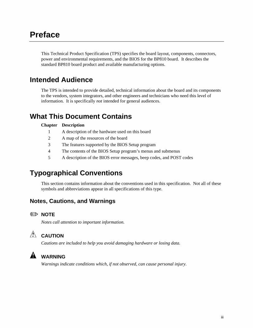
1.14.1.2 Wake Up Devices and EventsTable 10 lists the devices or specific events that can wake the computer from specific states.
Table 10. Wake Up Devices and Events
These devices/events can wake up the computer… …from this state
Power switch S3, S5
RTC alarm S3, S5
LAN S3, S5
Modem S1, S3
USB S1, S3
Note: S3 support requires the Intel 82801AA ICH1 component.
1.14.1.3 Plug and PlayIn addition to power management, ACPI provides controls and information so that the operatingsystem can facilitate Plug and Play device enumeration and configuration. ACPI is used only toenumerate and configure onboard devices that do not have other hardware standards forenumeration and configuration. PCI devices on the board, for example, are not enumeratedby ACPI.
1.14.2 Hardware Support
CAUTIONIf Wake on LAN and Instantly Available technology features are used, ensure that the power supplyprovides adequate +5 V standby current. Failure to do so can damage the power supply. The totalamount of standby current required depends on the wake devices supported and manufacturingoptions. Refer to Section 2.11.2 on page 57 for additional information.
The board provides several hardware features that support power management, including:
• Power connector• Fan connectors• Wake on LAN technology• Instantly Available technology• Wake on Ring• Resume on Ring• Wake from USB
Wake on LAN technology and Instantly Available technology require power from the +5 V standbyline. The sections discussing these features describe the incremental standby power requirementsfor each.
Wake on Ring and Resume on Ring enable telephony devices to access the computer when it is in apower-managed state. The method used depends on the type of telephony device (external orinternal) and the ACPI state being used.

Board Description
33
NOTEThe use of Wake on Ring, Resume on Ring, and Wake from USB technologies from an ACPI staterequire the support of an operating system and a peripheral device that provides full ACPIfunctionality.
1.14.2.1 Power ConnectorWhen used with an ATX-compliant power supply that supports remote power on/off, the board canturn off the system power through software control.
With soft-off enabled, if power to the computer is interrupted by a power outage or a disconnectedpower cord, when power resumes, the computer returns to the power state it was in before powerwas interrupted (on or off).
For information about Refer to
The location of the power connector Figure 8, page 46
The signal names of the power connector Table 26, page 47
The ATX specification Table 3, page 16
1.14.2.2 Fan ConnectorsThe board has two fan connectors, one of which is a manufacturing option. The functions of theseconnectors are described in Table 11.
Table 11. Fan Connector Descriptions
Connector Function
Processor fan Provides +12 V DC for a processor fan or active fan heatsink.
Chassis fan (optional) Provides +12 V DC for a system or chassis fan. The fan voltage can be switchedon or off, depending on the power management state of the computer.
For information about Refer to
The location of the fan connectors Figure 8, page 46
The signal names of the processor fan connector Table 24, page 47
The signal names of the chassis fan connector Table 30, page 49
1.14.2.3 Wake on LAN Technology
CAUTIONFor Wake on LAN technology, the 5-V standby line for the power supply must be capable ofdelivering adequate standby current. Failure to provide adequate standby current whenimplementing Wake on LAN technology can damage the power supply. Refer to Section 2.11.2 onpage 57 for additional information.
Wake on LAN technology enables remote wakeup of the computer through a network. The LANsubsystem, whether onboard or as a PCI bus network adapter, monitors network traffic at the MediaIndependent Interface. Upon detecting a Magic Packet† frame, the LAN subsystem asserts awakeup signal that powers up the computer. The board supports Wake on LAN technology throughthe PCI bus PME# signal.

Intel Desktop Board BP810 Technical Product Specification
34
1.14.2.4 Instantly Available Technology
CAUTIONFor Instantly Available technology, the 5-V standby line for the power supply must be capable ofdelivering adequate standby current. Failure to provide adequate standby current when using thisfeature can damage the power supply. Refer to Section 2.11.2 on page 57 for additionalinformation.
Instantly Available technology enables the board to enter the ACPI S3 (Suspend-to-RAM) sleep-state. While in the S3 sleep-state, the computer will appear to be off (the power supply is off, thefans are off, and the power LED is amber). When signaled by a wake-up device or event, thesystem quickly returns to its last known wake state. Table 10 on page 32 lists the devices andevents that can wake the computer from the S3 state. The use of Instantly Available technologyrequires:
• Operating system support• PCI 2.2 compliant add-in cards and drivers• The Intel 82801AA ICH1 component; boards with the 82801AB ICH0 component do not
support Instantly Available technology
The optional standby power indicator LED (located between the power connector and the DIMMsocket) provides an indication that power is still present to the DIMM, even when the computerappears to be off. Figure 5 shows the location of the standby power indicator LED.
OM08738
DS7F1
Figure 5. Location of Standby Power Indicator LED
Board Description
35
1.14.2.5 Wake on RingThe operation of Wake on Ring can be summarized as follows:
• Wakes the computer from an ACPI S3 state• Requires two calls to access the computer:
First call restores the computer
Second call enables access (when the appropriate software is loaded)• The onboard modem detects the incoming call through the AC ’97 Wake Up feature
1.14.2.6 Resume on RingThe operation of Resume on Ring can be summarized as follows:
• Resumes operation from the ACPI S1 state• Requires only one call to access the computer• The onboard modem detects the incoming call through the AC ’97 Wake Up feature
1.14.2.7 Wake from USBUSB bus activity wakes the computer from an ACPI S1 or S3 state.
NOTE
Wake from USB requires the use of a USB peripheral that supports the Wake from USB feature.

Intel Desktop Board BP810 Technical Product Specification
36

37
2 Technical Reference
What This Chapter Contains2.1 Introduction................................................................................................................ 372.2 Memory Map.............................................................................................................. 372.3 I/O Map...................................................................................................................... 382.4 DMA Channels .......................................................................................................... 392.5 PCI Configuration Space Map ................................................................................... 402.6 Interrupts ................................................................................................................... 402.7 PCI Interrupt Routing Map ......................................................................................... 41
2.1 IntroductionSections 2.2 – 2.6 contain several standalone tables. Table 12 describes the system memory map,Table 13 shows the I/O map, Table 14 lists the DMA channels, Table 15 defines the PCIconfiguration space map, and Table 16 describes the interrupts. The remaining sections in thischapter are introduced by text found with their respective section headings.
2.2 Memory Map
Table 12. System Memory Map
Address Range (decimal) Address Range (hex) Size Description
1024 K – 262144 K 100000 – FFFFFFF 255 MB Extended memory
960 K – 1024 K F0000 – FFFFF 64 KB Runtime BIOS
896 K – 960 K E0000 – EFFFF 64 KB Reserved
800 K – 896 K C8000 – DFFFF 96 KB Available high DOS memory (opento PCI bus)
640 K – 800 K A0000 – C7FFF 160 KB Video memory and BIOS
639 K – 640 K 9FC00 – 9FFFF 1 KB Extended BIOS data (movable bymemory manager software)
512 K – 639 K 80000 – 9FBFF 127 KB Extended conventional memory
0 K – 512 K 00000 – 7FFFF 512 K Conventional memory

Intel Desktop Board BP810 Technical Product Specification
38
2.3 I/O Map
Table 13. I/O Map
Address (hex) Size Description
0000 – 000F 16 bytes DMA Controller
0020 – 0021 2 bytes Programmable Interrupt Control (PIC)
0040 – 0043 4 bytes System Timer
0060 1 byte Keyboard controller byte – reset IRQ
0061 1 byte System Speaker
0064 1 byte Keyboard controller, CMD/STAT byte
0070 – 0071 2 bytes System CMOS / Real-Time Clock
0072 – 0073 2 bytes System CMOS
0080 – 008F 16 bytes DMA Controller
0092 1 byte Fast A20 and PIC
00A0 – 00A1 2 bytes PIC
00C0 – 00DF 32 bytes DMA
00F0 1 byte Numeric data processor
01F0 – 01F7 8 bytes Primary IDE channel
02E8 – 02EF1 8 bytes COM4/video (8514A)
02F8 – 02FF1 8 bytes COM2
03B0 – 03BB 12 bytes Intel 82810 – DC100 Graphics/Memory Controller Hub (GMCH)
03C0 – 03DF 32 byte Intel 82810 – Graphics/Memory Controller Hub (GMCH)
03E8 – 03EF 8 bytes COM3
03F0 – 03F5 6 bytes Diskette channel 1
03F6 1 byte Primary IDE channel command port
03F8 – 03FF 8 bytes COM1
04D0 – 04D1 2 bytes Edge/level triggered PIC
0CF8 – 0CFB2 4 bytes PCI configuration address register
0CF93 1 byte Turbo and reset control register
0CFC – 0CFF 4 bytes PCI configuration data register
FFA0 – FFA7 8 bytes Primary bus master IDE registers
96 contiguous bytes starting on a128-byte divisible boundary
ICH (ACPI + TCO)
64 contiguous bytes starting on a64-byte divisible boundary
Onboard resources
256 contiguous bytes starting ona 256-byte divisible boundary
ICH audio mixer
64 contiguous bytes starting on a64-byte divisible boundary
ICH audio bus master
256 contiguous bytes starting ona 256-byte divisible boundary
ICH modem mixer
continued

Technical Reference
39
Table 13. I/O Map (continued)
Address (hex) Size Description
16 contiguous bytes starting on a16-byte divisible boundary
ICH (SMBus)
32 contiguous bytes starting on a32-byte divisible boundary
ICH (USB)
4096 contiguous bytes starting ona 4096-byte divisible boundary
Intel 82810 PCI Bridge
128 contiguous bytes starting ona 128-byte divisible boundary
Intel 21145 Phoneline/Ethernet LAN controller
Notes:
1. Default, but can be changed to another address range
2. Dword access only
3. Byte access only
NOTESome additional I/O addresses are not available due to ICH addresses aliasing. For informationabout ICH addressing, refer to Intel web site at:
http://developer.intel.com/design/chipsets/datashts/
2.4 DMA Channels
Table 14. DMA Channels
DMA Channel Number Data Width System Resource
0 8- or 16-bits Open
1 8- or 16-bits Open
2 8- or 16-bits Diskette Drive
3 8- or 16-bits Open
4 Reserved - cascade channel
5 16-bits Open
6 16-bits Open
7 16-bits Open

Intel Desktop Board BP810 Technical Product Specification
40
2.5 PCI Configuration Space Map
Table 15. PCI Configuration Space Map
BusNumber (hex)
DeviceNumber (hex)
FunctionNumber (hex) Description
00 00 00 Memory controller of Intel 82810 component
00 01 00 Graphics controller of Intel 82810 component
00 1E 00 Link to PCI bridge
00 1F 00 PCI-to-LPC bridge
00 1F 01 IDE controller
00 1F 02 USB controller
00 1F 03 SMBus controller
00 1F 04 Reserved
00 1F 05 AC ’97 audio controller
00 1F 06 AC ’97 modem controller
01 01 00 Intel 21145 Phoneline/Ethernet LAN controller
2.6 Interrupts
Table 16. Interrupts
IRQ System Resource
NMI I/O channel check
0 Reserved, interval timer
1 Reserved, keyboard buffer full
2 Reserved, cascade interrupt from slave PIC
3 User available
4 COM1 (Note)
5 User available
6 Diskette drive
7 User available
8 Real-Time Clock
9 Reserved for ICH system management bus
10 Audio / Modem
11 Video
12 User available
13 Reserved, math coprocessor
14 Primary IDE (if present, else user available)
15 Network / User available
Note: Default, but can be changed to another IRQ

Technical Reference
41
2.7 PCI Interrupt Routing MapThis section describes interrupt sharing and how the interrupt signals are connected between thePCI bus connectors and onboard PCI devices. The PCI specification specifies how interrupts canbe shared between devices attached to the PCI bus. In most cases, the small amount of latencyadded by interrupt sharing does not affect the operation or throughput of the devices. In somespecial cases where maximum performance is needed from a device, a PCI device should not sharean interrupt with other PCI devices.
PCI devices are categorized as follows to specify their interrupt grouping:
• INTA: By default, all add-in devices that require only one interrupt are in this category. Foralmost all devices that require more than one interrupt, the first interrupt on the device is alsoclassified as INTA.
• INTB: Generally, the second interrupt on add-in devices that require two or more interrupts isclassified as INTB. (This is not an absolute requirement.)
• INTC and INTD: Generally, a third interrupt on add-in devices is classified as INTC and afourth interrupt is classified as INTD.
The ICH PCI-to-LPC bridge has four programmable interrupt request (PIRQ) input signals. AnyPCI interrupt source connects to one of these PIRQ signals. Because there are only four signals,some PCI interrupt sources are mechanically tied together on the board and therefore share thesame interrupt. Table 17 lists the PIRQ signals and shows how the signals are connected to theonboard PCI interrupt sources.
Table 17. PCI Interrupt Routing Map
ICH PIRQ Signal NamePCI Interrupt Source PIRQA PIRQB PIRQC PIRQD
AGP Controller INTA INTB
ICH Audio Controller INTB
ICH Modem Controller INTB
ICH USB Controller INTD
Intel 21145 INTA
NOTEThe ICH can connect each PIRQ line internally to one of the IRQ signals (3, 4, 5, 7, 9, 10, 11, 14,and 15). Typically, a device that does not share a PIRQ line will have a unique interrupt.However, in certain interrupt-constrained situations, it is possible for two or more of the PIRQlines to be connected to the same IRQ signal.

Intel Desktop Board BP810 Technical Product Specification
42
2.8 Connectors
CAUTIONOnly the back panel connectors of this board have overcurrent protection. The internal boardconnectors are not overcurrent protected, and should connect only to devices inside the computerchassis, such as fans and internal peripherals. Do not use these connectors for powering devicesexternal to the computer chassis. A fault in the load presented by the external devices could causedamage to the computer, the interconnecting cable, and the external devices themselves.
This section describes the board’s connectors. The connectors can be divided into three groups, asshown in Figure 6.
OM08739
B
A
C
A. Back panel connectors(see page 43)
B. Midboard connectors(see page 46)
C. Front panel connector(see page 50)
Figure 6. Connector Groups

Technical Reference
43
2.8.1 Back Panel ConnectorsFigure 7 shows the location of the back panel connectors.
OM08679C F
E
GDA B
Item Description For more information, see…A USB port 0 Table 18, page 44B USB port 1 Table 18, page 44C VGA port Table 19, page 44D LAN Table 20, page 44E Audio line out Table 21, page 45F Mic in Table 22, page 45G Telephone jack Table 23, page 45
Figure 7. Back Panel Connectors
NOTE
The back panel audio line out connector is designed to power headphones or amplified speakersonly. Poor audio quality may occur if passive (non-amplified) speakers are connected to thisoutput.

Intel Desktop Board BP810 Technical Product Specification
44
Table 18. USB Connectors
Pin Signal Name
1 +5 V (fused)
2 USBP0# / USBP1#
3 USBP0 / USBP1
4 Ground
Table 19. VGA Port Connector
Pin Signal Name
1 Red
2 Green
3 Blue
4 No connect
5 Ground
6 Ground
7 Ground
8 Ground
9 Fused VCC
10 Ground
11 No connect
12 MONID1
13 HSYNC
14 VSYNC
15 MONID2
Table 20. LAN Connector (Optional)
Pin Signal Name
1 TX+
2 TX-
3 RX+
4 Ground
5 Ground
6 RX-
7 Ground
8 Ground
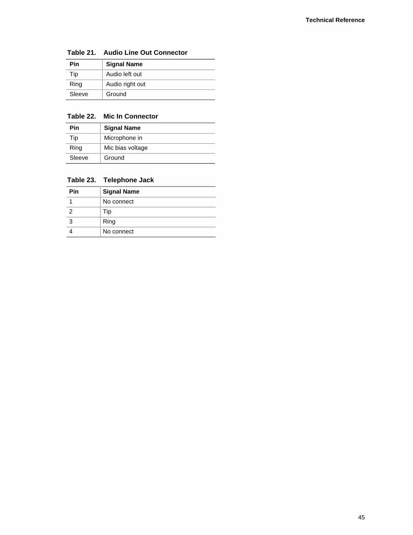
Technical Reference
45
Table 21. Audio Line Out Connector
Pin Signal Name
Tip Audio left out
Ring Audio right out
Sleeve Ground
Table 22. Mic In Connector
Pin Signal Name
Tip Microphone in
Ring Mic bias voltage
Sleeve Ground
Table 23. Telephone Jack
Pin Signal Name
1 No connect
2 Tip
3 Ring
4 No connect

Intel Desktop Board BP810 Technical Product Specification
46
2.8.2 Midboard ConnectorsFigure 8 shows the location of the midboard connectors.
OM08740
1
24039
1
A
1
23334
1
111
1020
CDE B
107
21
89
21
G
F
Item Description Reference Designator For more information, see…
A Processor fan J5J1 Table 24, page 47
B Front panel USB J7G1 Table 25, page 47
C Power J7G3 Table 26, page 47
D Diskette drive J7D1 Table 27, page 48
E Serial port J7B2 Table 28, page 48
F IDE J7B1 Table 29, page 49
G Chassis fan J3A2 Table 30, page 49
Figure 8. Midboard Connectors
For information about Refer to
The power connector Section 1.14.2.1, page 33
The functions of the fan connectors Section 1.14.2.2, page 33

Technical Reference
47
Table 24. Processor Fan Connector (J5J1)
Pin Signal Name
1 Ground
2 +12 V
3 Ground
Table 25. Front Panel USB (J7G1)
Pin Signal Name Pin Signal Name
1 VREG_USB2_PWR 2 VREG_USB2_PW
3 USB_DM3 4 USB_DM4
5 USB_DP3 6 USB_DP4
7 Ground 8 Ground
9 Key (no pin) 10 No connect
Table 26. Power Connector (J7G3)
Pin Signal Name Pin Signal Name
1 +3.3 V 11 +3.3 V
2 +3.3 V 12 -12 V
3 Ground 13 Ground
4 +5 V 14 PS-ON# (power supply remote on/off)
5 Ground 15 Ground
6 +5 V 16 Ground
7 Ground 17 Ground
8 PWRGD (Power Good) 18 -5 V
9 +5 VSB 19 +5 V
10 +12 V 20 +5 V

Intel Desktop Board BP810 Technical Product Specification
48
Table 27. Diskette Drive Connector (J7D1)
Pin Signal Pin Signal
1 Ground 2 DENSEL
3 Ground 4 No connect
5 Key 6 FDEDIN
7 Ground 8 FDINDX# (Index)
9 Ground 10 FDM00# (Motor Enable A)
11 Ground 12 No connect
13 Ground 14 FDDS0# (Drive Select A)
15 Ground 16 No connect
17 No connect 18 FDDIR# (Stepper Motor Direction)
19 Ground 20 FDSTEP# (Step Pulse)
21 Ground 22 FDWD# (Write Data)
23 Ground 24 FDWE# (Write Enable)
25 Ground 26 FDTRK0# (Track 0)
27 No connect 28 FDWPD# (Write Protect)
29 Ground 30 FDRDATA# (Read Data)
31 Ground 32 FDHEAD# (Side 1 Select)
33 Ground 34 DSKCHG# (Diskette Change)
Table 28. Serial Port Connector (J7B2)
Pin Signal Name Pin Signal Name
1 DCD (Data Carrier Detect) 2 DSR (Data Set Ready)
3 SIN # (Serial Data In) 4 RTS (Request to Send)
5 SOUT # (Serial Data Out) 6 CTS (Clear to Send)
7 DTR (Data Terminal Ready) 8 RI (Ring Indicator)
9 Ground 10 Key (no pin)

Technical Reference
49
Table 29. IDE Connector (J7B1)
Pin Signal Name Pin Signal Name
1 Reset IDE 2 Ground
3 Data 7 4 Data 8
5 Data 6 6 Data 9
7 Data 5 8 Data 10
9 Data 4 10 Data 11
11 Data 3 12 Data 12
13 Data 2 14 Data 13
15 Data 1 16 Data 14
17 Data 0 18 Data 15
19 Ground 20 Key
21 DDRQ0 22 Ground
23 I/O Write# 24 Ground
25 I/O Read# 26 Ground
27 IOCHRDY 28 Ground
29 DDACK0# 30 Ground
31 IRQ 14 32 Reserved
33 DAG1 (Address 1) 34 DMA66_DETECT
35 DAG0 (Address 0) 36 DAG2 (Address 2)
37 Chip Select 1P# 38 Chip Select 3P#
39 Activity# 40 Ground
Table 30. Chassis Fan Connector (J3A2)
Pin Signal Name
1 Ground
2 +12 V
3 FAN_TACH1

Intel Desktop Board BP810 Technical Product Specification
50
2.8.3 Front Panel ConnectorFigure 9 shows the location of the front panel connector. Table 31 lists the signal names of thefront panel connector.
OM08737
2 18
171 J7G2
21
1817
C D
A B
Item Pins Description
A 2 and 4 Power / Sleep / Message waiting LED
B 6 and 8 Power switch
C 1 and 3 Hard drive activity LED
D 5 and 7 Reset switch
Figure 9. Front Panel Connector

Technical Reference
51
Table 31. Front Panel Connector (J7G2)
Pin Signal In/Out Description Pin Signal In/Out Description
1 HD_PWR Out Hard disk LED pull-up (330 Ω) to +5 V
2 GREEN_BLINK
Out Front panel greenLED
3 HD_LED# Out Hard disk active LED 4 YELLOW_BLINK
Out Front panel yellowLED
5 GND Ground 6 SWITCH_ON#
In Power switch
7 FP_RST# In Reset switch 8 GND Ground
9 +5 V Power 10 No connect No connect
11 No connect No connect 12 GND Ground
13 GND Ground 14 (pin removed) Not connected
15 No connect No connect 16 +5 V Power
17 +5 V Power 18 No connect No connect
2.8.3.1 Power / Sleep / Message Waiting LED ConnectorPins 2 and 4 can be connected to a single- or dual-colored LED. Table 32 shows the possible statesfor a single-colored LED.
Table 33 shows the possible states for a dual-colored LED.
Table 32. States for a Single-colored Power LED
LED State Description
Off Power off
Steady Green Running
Blinking Green Running/message waiting
Table 33. States for a Dual-colored Power LED
LED State Description
Off Power off
Steady Green Running
Blinking Green Running/message waiting
Steady Yellow Sleeping
Blinking Yellow Sleeping/message waiting
NOTETo use the message waiting function, ACPI must be enabled in the operating system and a message-capturing application must be invoked.

Intel Desktop Board BP810 Technical Product Specification
52
2.8.3.2 Power Switch ConnectorPins 6 and 8 can be connected to a front panel power switch. The switch must pull the SW_ON#pin to ground for at least 50 ms to signal the power supply to switch on or off. (The timerequirement is due to internal debounce circuitry on the board.) At least two seconds must passbefore the power supply will recognize another on/off signal.
2.8.3.3 Hard Drive Activity LED ConnectorPins 1 and 3 can be connected to an LED to provide a visual indicator that data is being read fromor written to a hard drive. For the LED to function properly, an IDE drive must be connected to theonboard IDE interface.
2.8.3.4 Reset Switch ConnectorPins 5 and 7 can be connected to a momentary SPST type switch that is normally open. When theswitch is closed, the board resets and runs the POST.

Technical Reference
53
2.9 Jumper Block
CAUTIONDo not move any jumpers with the power on. Always turn off the power and unplug the power cordfrom the computer before changing a jumper setting. Otherwise, the board could be damaged.
Figure 10 shows the location of the BIOS Setup jumper block. This 3-pin jumper block determinesthe BIOS Setup program’s mode. Table 34 describes the jumper settings for the three modes:normal, configure, and recovery.
1
3J5A1
OM08736
Figure 10. Location of the Jumper Block

Intel Desktop Board BP810 Technical Product Specification
54
Table 34. BIOS Setup Configuration Jumper Settings (J5A1)
Function/Mode Jumper Setting Configuration
Normal1-2
1 3 The BIOS uses current configuration information andpasswords for booting.
Configure2-3
1 3 After the POST runs, Setup runs automatically. Themaintenance menu is displayed.
RecoveryNone
1 3 The BIOS attempts to recover the BIOS configuration. Arecovery diskette is required.
For information about Refer to
How to access the BIOS Setup program Section 4.1, page 75
The maintenance menu of the BIOS Setup program Section 4.2, page 76
BIOS recovery Section 3.6, page 70

Technical Reference
55
2.10 Mechanical Considerations
2.10.1 FlexATX Form FactorThe board is designed to fit into an ATX- or microATX-form-factor chassis. Figure 11 illustratesthe mechanical form factor for the board. Dimensions are given in inches. The outer dimensionsare 9.0 inches by 7.2 inches. Location of the I/O connectors and mounting holes are in compliancewith the FlexATX addendum of the microATX specification (see Section 1.3).
OM08735
6.10
6.80
0.75 8.25
0.90
0.40
1.80 8.00
0.00
0.00
Figure 11. Board Dimensions

Intel Desktop Board BP810 Technical Product Specification
56
2.10.2 I/O ShieldThe back panel I/O shield for the board must meet specific dimension and material requirements.Systems based on this board need the back panel I/O shield to pass certification testing. Figure 12shows the critical dimensions of the I/O shield for versions of the board without the RJ-45 LANconnector. Dimensions are given in inches. For dimensions given to two decimal places, (X.XX)the tolerance is ±0.02 inches. The figure indicate the position of each cutout. Additional designconsiderations for I/O shields relative to chassis requirements are described in the ATXspecification. See Section 1.3 for information about the ATX specification.
24.00
12.02717.366
22.45
0.00
0.00
53.8
9
74.3
09
133.
59
142.
774
OM08906
PictorialViews
24.0022.45
R .50Min Typ
2x Dia 8.50
1.55Ref
159.20
20.00 ± .26 Typ.
162.30 Ref
48.00Ref
11.697
3.289
17.764
15.00 ± .26Typ
44.90Right-end View
Figure 12. I/O Shield Dimensions (without LAN Connector)

Technical Reference
57
2.11 Electrical Considerations
2.11.1 Power ConsumptionTable 35 lists voltage and current specifications for a computer that contains the board and thefollowing:
• 500 MHz Intel Celeron processor with a 128 KB cache• 128 MB SDRAM• 3.5-inch diskette drive• 3.2 GB IDE hard disk drive• 40X IDE CD-ROM drive
This information is provided only as a guide for calculating approximate power usage withadditional resources added.
Values for the Windows 98 desktop mode are measured at 640 x 480 x 256 colors and 60 Hzrefresh rate. AC watts are measured with a typical 145 W power supply, nominal input voltage andfrequency, with true RMS wattmeter at the line input.
Table 35. Power Usage
DC Current at:
Mode AC Power +3.3 V +5 V +12 V -12 V +5 VSB
Windows 98 ACPI S0 27 W 1.24 A 0.612 A 0.143 A 0.057A 0.273 A
Windows 98 ACPI S1 22 W 1.14 A 0.554 A 0.143 A 0.005A 0.192 A
Windows 98 ACPI S3 2 W 0.001 A 0.001 A 0.001 A 0.001 A 0.188 A
2.11.2 Power Supply ConsiderationsSystem integrators should refer to the power usage values listed in Table 35 when selecting a powersupply for use with this board. The power supply must comply with the followingrecommendations found in the indicated sections of the ATX form factor specification(see Section 1.3).
• The potential relation between 3.3 VDC and +5 VDC power rails (Section 4.2)• The current capability of the +5 VSB line (Section 4.2.1.2)• All timing parameters (Section 4.2.1.3)• All voltage tolerances (Section 4.2.2)

Intel Desktop Board BP810 Technical Product Specification
58
2.11.3 Standby Current RequirementsTable 36 lists the +5 V standby current consumed by the board itself in two configurations.
Table 36. Standby Current Usage
Configuration +5 V Standby Current Required
Board without onboard networking 0.102 A
Board with onboard networking 0.185 A
NOTE
These standby current requirements are system configuration dependent.
2.11.4 Fan Power RequirementsTable 37 lists the maximum DC voltage and current requirements for the chassis fan when theboard is in normal operating mode, sleep mode, or Suspend-to-RAM state. Power consumption isindependent of the operating system used and other variables.
Table 37. Chassis Fan (J3A2) DC Power Requirements
Mode Voltage Maximum Current
Normal (S0) +12 VDC 0.174 A (current limited)
Sleep (S1) +12 VDC 0.174 A (current limited)
Suspend-to-RAM (S3) 0.0 VDC 0.0 A
For information about Refer to
The location of the chassis fan connector Figure 8, page 46
The signal names of the chassis fan connector Table 30, page 49

Technical Reference
59
2.12 Thermal Considerations
CAUTIONAn ambient temperature that exceeds the board’s maximum operating temperature by 5 oC to 10 oCcould cause components to exceed their maximum case temperature and malfunction. Forinformation about the maximum operating temperature, see the environmental specifications inSection 2.14.
Figure 13 shows the locations of the thermally-sensitive components.
OM08734
B
C
A
A Processor voltage regulator area
B Processor
C Intel 82810 GMCH
Figure 13. Thermally-sensitive Components

Intel Desktop Board BP810 Technical Product Specification
60
Table 38 provides maximum component case temperatures for board components that could besensitive to thermal changes. Case temperatures could be affected by the operating temperature,current load, or operating frequency. Maximum case temperatures are important when consideringproper airflow to cool the board.
Table 38. Thermal Considerations for Components
Component Maximum Case Temperature
Celeron Processor 300A MHz 85 °C
333 MHz 85 °C
366 MHz 85 °C
400 MHz 85 °C
433 MHz 85 °C
466 MHz 85 °C
500 MHz 85 °C
Intel 82810 GMCH 70 °C
CAUTIONThe voltage regulator area can reach a temperature of up to 85 oC in an open chassis. Ensure thatthere is proper airflow to this area of the board. Failure to do so may result in damage to thevoltage regulator circuit. System integrators should ensure that proper airflow is maintained in thevoltage regulator circuit (item C in Figure 13). Components in this area could be damaged withoutadequate airflow.
2.13 ReliabilityThe mean time between failures (MTBF) prediction is calculated using component andsubassembly random failure rates. The calculation is based on the Bellcore Reliability PredictionProcedure, TR-NWT-000332, Issue 4, September 1991. The MTBF prediction is used to estimaterepair rates and spare parts requirements. MTBF data is calculated from predicted data at 55 ºC.
Board MTBF:
• 201,905 hours (without onboard networking)• 177,507 hours (with onboard networking)

Technical Reference
61
2.14 EnvironmentalTable 39 lists the environmental specifications for the board.
Table 39. Board Environmental Specifications
Parameter Specification
Temperature
Non-Operating -40 °C to +70 °C
Operating 0 °C to +55 °C
Shock
Unpackaged 30 g trapezoidal waveform
Velocity change of 170 inches/second
Packaged Half sine 2 millisecond
Product Weight (pounds) Free Fall (inches) Velocity Change (inches/sec)
<20 36 167
21-40 30 152
41-80 24 136
81-100 18 118
Vibration
Unpackaged 5 Hz to 20 Hz : 0.01 g² Hz sloping up to 0.02 g² Hz
20 Hz to 500 Hz : 0.02 g² Hz (flat)
Packaged 10 Hz to 40 Hz : 0.015 g² Hz (flat)
40 Hz to 500 Hz : 0.015 g² Hz sloping down to 0.00015 g² Hz
2.15 Regulatory ComplianceThis section describes the board’s compliance with safety and EMC regulations.
2.15.1 Safety RegulationsTable 40 lists the safety regulations the board complies with when it is correctly installed in acompatible host system.
Table 40. Safety Regulations
Regulation Title
UL 1950/CSA950, 2nd edition,Dated 26 February 1993
Bi-National Standard for Safety of Information Technology Equipmentincluding Electrical Business Equipment. (USA and Canada)
EN 60950, 2nd Edition, 1992(with Amendments 1, 2, 3, and 4)
The Standard for Safety of Information Technology Equipment includingElectrical Business Equipment. (European Community)
IEC 950, 2nd edition, 1991 (withAmendments 1, 2, 3, and 4)
The Standard for Safety of Information Technology Equipment includingElectrical Business Equipment. (International)
EMKO-TSE (74-SEC) 207/94 Summary of Nordic deviations to EN 60950. (Norway, Sweden,Denmark, and Finland)

Intel Desktop Board BP810 Technical Product Specification
62
2.15.2 EMC RegulationsTable 41 lists the EMC regulations the board complies with when it is correctly installed in acompatible host system.
Table 41. EMC Regulations
Regulation Title
FCC Class B Title 47 of the Code of Federal Regulations, Parts 2 and 15, Subpart B,pertaining to unintentional radiators. (USA)
CISPR 22, 2nd Edition,1993 (Class B)
Limits and methods of measurement of Radio Interference Characteristics ofInformation Technology Equipment. (International)
VCCI Class B (ITE) Implementation Regulations for Voluntary Control of Radio Interference byData Processing Equipment and Electronic Office Machines. (Japan)
EN55022 (1994) (Class B) Limits and methods of measurement of Radio Interference Characteristics ofInformation Technology Equipment. (Europe)
EN50082-1 (1992) Generic Immunity Standard; Currently compliance is determined via testing toIEC 801-2, -3, and -4. (Europe)
ICES-003 (1997) Interference-Causing Equipment Standard, Digital Apparatus, Class B(Including CRC c.1374). (Canada)
AS/NZ 3548 Australian Communications Authority (ACA), Standard for ElectromagneticCompatibility.
2.15.3 Telecommunications RegulationsTable 42 lists the telecommunications regulations the board complies with when it is correctlyinstalled in a compatible host system.
Table 42. Telecommunications Regulations
Regulation Title
FCC Part 68 Title 47 of the Code of Federal Regulations, Part 68, Connection of TerminalEquipment to the Telephone Network
CS 03 Issue 8 (1996) Harmonized Requirements for Terminal Equipment, Terminal Systems, andCertified Protection Circuitry
CTR21 Council Decision 98/482/EC On a Common Technical Regulation for theAttachment Requirements for Connection to the Analogue Public SwitchedTelephone Networks (PSTNs) of Terminal Equipment (Excluding TerminalEquipment Supporting the Voice Telephony Justified Case Service) in WhichNetwork Addressing, if Provided, is by Means of Dual Tone Multi-Frequency(DTMF) Signalling
ETSI Guide 201 121 Advisory Notes for CTR21
TS001 Safety Requirements for Customer Equipment
TS002 Analogue Interworking and Non-Interference
PTC200 Requirements for Analogue Telecommunications Equipment
TS PSTN1 TAS Type Approval Specification for Connection of Terminal Equipment to PublicSwitched Telephone Network
PW-TFI SIRIM
JATE Blue Book For Analog Telephone Terminals

Technical Reference
63
2.15.4 Certification MarkingsThis printed circuit assembly has the following product certification markings:
• UL Joint Recognition Mark: Consists of small c followed by a stylized backward UR andfollowed by a small US (Component side)
• Manufacturer’s recognition mark: Consists of a unique UL recognized manufacturer’s logo,along with a flammability rating (94V-0) (Solder side)
• UL File Number for desktop boards: E139761 (Component side)• PB Part Number: Intel bare circuit board part number (Solder side) 741674-002• Battery “+ Side Up” marking: located on the component side of the board in close proximity to
the battery holder• FCC Part 15 Class B Logo/Declaration: (Solder side)• FCC Part 68 Declaration: Includes the part 68 certificate number of the format EJMxxx-
xxxxx-xx-x, followed by the REN number in the format x.xB. In addition for Canadiancompliance add the Canadian REN number in the format x.xA
• ACA (A-Tick) mark: Consists of a unique triangle, with a tick mark; followed by N-232.Located on the component side of the board and on the shipping container.
• CE Mark with CTR 21 additions: (Component side) This mark consists of the CE markfollowed by the number of the Notified Body that approved the product followed by the CTR21symbol of “crossed hockey sticks”. The CE mark should also be on the shipping container.The additions for CTR21 (Notified Body number and “crossed hockey sticks”) are not requiredon the shipping container.
There are requirements for some countries in addition to the silk-screened items above. Some ofthe these requirements are additional labels that cannot be silk-screened onto the board, includingthe following:
• The Canadian Telecommunication Label must be affixed to the board. These are purchasedseparately from Canada.
• The Telepermit label must be on the board. It can be incorporated into a label that containsother approval marks. It has color requirements. See Telepermit for size and colorrequirements. There is an approval number in the format PTCxxx/xx/xxx.
• The TAS label or mark must be on the board. It can be incorporated into a label that containsother approval marks. There is an approval number in the format xxxxx-xxxx-xx-xxxx-xx.
• The Japan Telecom label must be on the board. It can be incorporated into a label that containsother approval marks. There is an approval number in the format xxx-xxxx-x.

Intel Desktop Board BP810 Technical Product Specification
64

65
3 Overview of BIOS Features
What This Chapter Contains3.1 Introduction................................................................................................................ 653.2 BIOS Flash Memory Organization ............................................................................. 663.3 Resource Configuration ............................................................................................. 673.4 System Management BIOS (SMBIOS) ...................................................................... 683.5 BIOS Upgrades ......................................................................................................... 693.6 Recovering BIOS Data .............................................................................................. 703.7 Boot Options.............................................................................................................. 713.8 USB Legacy Support ................................................................................................. 723.9 BIOS Security Features ............................................................................................. 73
3.1 IntroductionThe board uses an Intel/AMI BIOS, which is stored in flash memory and can be upgraded using adisk-based program. In addition to the BIOS, the flash memory contains the BIOS Setup program,POST, the PCI auto-configuration utility, and Plug and Play support.
This board supports system BIOS shadowing, allowing the BIOS to execute from 64-bit onboardwrite-protected DRAM.
The BIOS displays a message during POST identifying the type of BIOS and a revision code. Theinitial production BIOS is identified as BP81010A.86A.
For information about Refer to
The board’s compliance level with Plug and Play Table 3, page 16

Intel Desktop Board BP810 Technical Product Specification
66
3.2 BIOS Flash Memory OrganizationThe Intel 82802AB Firmware Hub (FWH) includes a 4 Mbit (512 KB) symmetrical flash memorydevice. Internally, the device is grouped into eight 64-KB blocks that are individually erasable,lockable, and unlockable. Figure 14 shows the organization of the flash memory.
The last two 8 KB blocks of the fault tolerance area are the parameter blocks. These blocks containdata such as BIOS updates, vital product data (VPD), logo, System Management BIOS (SMBIOS)interface, and extended system configuration data (ESCD) information. The backup block containsa copy of the fault tolerance block.
64 KB Block 7
64 KB Block 6
64 KB Block 5
64 KB Block 4
64 KB Block 3
64 KB Block 2
64 KB Block 1
64 KB Block 0
Fault Tolerance
Main System BIOS
Backup
Boot Block
08000007FFFF07000006FFFF06000005FFFF05000004FFFF04000003FFFF03000002FFFF02000001FFFF01000000FFFF000000
OM08376
48 KB - Reserved
8 KB - Parameter Block 2
8 KB - Parameter Block 1
Figure 14. Memory Map of the Flash Memory Device

Overview of BIOS Features
67
3.3 Resource Configuration
3.3.1 PCI AutoconfigurationThe BIOS can automatically configure PCI devices. When a user turns on the system, the BIOSautomatically configures interrupts, the I/O space, and other system resources. Onboard PCIdevices can share an interrupt. Autoconfiguration information is stored in ESCD format.
For information about Refer to
The BIOS’s compliance level with Plug and Play Table 3, page 16
3.3.2 PCI IDE SupportIf you select Auto in the BIOS Setup program, the BIOS automatically sets up thePCI IDE connector with independent I/O channel support. The IDE interface supports hard drivesup to ATA/66 and recognizes any ATAPI devices, including CD-ROM drives, tape drives, andUltra DMA drives (see Section 1.3 for the supported version of ATAPI). The BIOS determines thecapabilities of each drive and configures them to optimize capacity and performance. To takeadvantage of the high capacities typically available today, hard drives are automatically configuredfor Logical Block Addressing (LBA) and to PIO Mode 3 or 4, depending on the capability of thedrive. You can override the auto-configuration options by specifying manual configuration in theBIOS Setup program.
To use ATA-66 features the following items are required:
• An ATA-66 peripheral device• An ATA-66 compatible cable• ATA-66 operating system device drivers• The 82801AA ICH1 component
NOTE
ATA-66 compatible cables are backward compatible with drivers using slower IDE transferprotocols. If an Ultra ATA/66 disk drive and a disk drive using any other IDE transfer protocol areattached to the same cable, the maximum transfer rate for either drive is 33 MB/sec.
NOTE
Do not connect an ATA device as a slave on the same IDE cable as an ATAPI master device. Forexample, do not connect an ATA hard drive as a slave to an ATAPI CD-ROM drive.

Intel Desktop Board BP810 Technical Product Specification
68
3.4 System Management BIOS (SMBIOS)SMBIOS is a Desktop Management Interface (DMI) compliant method for managing computers ina managed network.
The main component of SMBIOS is the management information format (MIF) database, whichcontains information about the computing system and its components. Using SMBIOS, a systemadministrator can obtain the system types, capabilities, operational status, and installation dates forsystem components. The MIF database defines the data and provides the method for accessing thisinformation. The BIOS enables applications such as Intel® LANDesk® Client Manager to useSMBIOS. The BIOS stores and reports the following SMBIOS information:
• BIOS data, such as the BIOS revision level• Fixed-system data, such as peripherals, serial numbers, and asset tags• Resource data, such as memory size, cache size, and processor speed• Dynamic data, such as event detection and error logging
Non-Plug and Play operating systems, such as Windows NT†, require an additional interface forobtaining the SMBIOS information. The BIOS supports an SMBIOS table interface for suchoperating systems. Using this support, an SMBIOS service-level application running on a non-Plug and Play operating system can obtain the SMBIOS information.
For information about Refer to
The board’s compliance level with SMBIOS Table 3, page 16

Overview of BIOS Features
69
3.5 BIOS UpgradesA new version of the BIOS can be upgraded from a diskette using the Intel® Flash Memory Updateutility that is available from Intel. This utility supports the following BIOS maintenance functions:
• Update the flash BIOS from a file on a diskette• Change the language section of the BIOS• Verify that the upgrade BIOS matches the target system to prevent accidentally installing an
incompatible BIOS• BIOS boot block update
BIOS upgrades and the Intel Flash Memory Update utility are available from Intel through the IntelWorld Wide Web site.
NOTE
Please review the instructions distributed with the upgrade utility before attempting a BIOSupgrade.
For information about Refer to
The Intel World Wide Web site Section 1.2, page 16
3.5.1 Language SupportThe BIOS Setup program and help messages can be supported in 32 languages. Five languages areavailable in the BIOS: US English, German, Italian, French, and Spanish. The default language isUS English, which is present unless another language is selected in the BIOS Setup program.
The BIOS includes extensions to support the Kanji character set and other non-ASCII charactersets. Translations of other languages may become available at a later date.
3.5.2 Custom Splash ScreenDuring POST, an Intel splash screen is displayed by default. This splash screen can be replacedwith a custom splash screen. A utility is available from Intel to assist with creating a custom splashscreen. The custom splash screen can be programmed into the flash memory using the BIOSupgrade utility. Information about this capability is available on the Intel Support World WideWeb site.
For information about Refer to
The Intel World Wide Web site Section 1.2, page 16

Intel Desktop Board BP810 Technical Product Specification
70
3.6 Recovering BIOS DataSome types of failure can destroy the BIOS. For example, the data can be lost if a power outageoccurs while the BIOS is being updated in flash memory. The BIOS can be recovered from adiskette using the BIOS recovery mode. When recovering the BIOS, be aware of the following:
• Because of the small amount of code available in the nonerasable boot block area, there is novideo support. You can only monitor this procedure by listening to the speaker or looking atthe diskette drive LED.
• The recovery process may take several minutes; larger BIOS flash memory devices requiremore time.
• A single beep indicates the beginning of the BIOS recovery process.• Two beeps and the end of activity in the diskette drive indicate successful BIOS recovery.• A series of continuous beeps indicates a failed BIOS recovery.
To create a BIOS recovery diskette, a bootable diskette must be created and the BIOS update filescopied to it. BIOS upgrades and the Intel Flash Memory Upgrade utility are available from IntelCustomer Support through the Intel World Wide Web site.
NOTEBIOS Recovery cannot be accomplished using non-SPD DIMMs. SPD data structure is requiredfor the recovery process.
NOTEIf the computer is configured to boot from an LS-120 diskette (in the Removable Devices submenu),the BIOS recovery diskette must be a standard 1.44 MB diskette not a 120 MB diskette.
For information about Refer to
The BIOS recovery mode Section 2.9, page 53
The Boot menu in the BIOS Setup program Section 4.6, page 83
Contacting Intel customer support Section 1.2, page 16
Overview of BIOS Features
71
3.7 Boot OptionsIn the BIOS Setup program, the user can choose to boot from a diskette drive, hard drives, or aCD-ROM drive. The default setting is for the diskette drive to be the primary boot device and thehard drive to be the secondary boot device. By default, the third and fourth devices are disabled.
3.7.1 Booting from CD-ROMBooting from CD-ROM is supported in compliance to the El Torito bootable CD-ROM formatspecification. Under the Boot menu in the BIOS Setup program, ATAPI CD-ROM is listed as aboot device. Boot devices are defined in priority order. If the CD-ROM is selected as the bootdevice, it must be the first device.
For information about Refer to
The El Torito specification Table 3, page 16
3.7.2 Booting Without Attached DevicesFor use in embedded applications, the BIOS has been designed so that after passing the POST, theoperating system loader is invoked even if the keyboard and mouse are not present.

Intel Desktop Board BP810 Technical Product Specification
72
3.8 USB Legacy SupportUSB legacy support enables USB keyboards, mice, and hubs to be used even when no operatingsystem USB drivers are in place. USB legacy support is used in accessing the BIOS Setup programand installing an operating system that supports USB. USB legacy support is automatically enabledwhenever a USB device is connected to a USB port. This sequence describes how USB legacysupport operates:
1. When you power up the computer, USB legacy support is enabled if a USB device is connectedto a USB port.
2. POST begins.3. USB legacy support is still enabled by the BIOS. This allows you to use a USB keyboard to
enter the BIOS Setup program or the maintenance mode.4. POST completes.5. The operating system loads. While the operating system is loading, USB keyboards and mice
are recognized. After the operating system loads the USB drivers, the USB devices arerecognized by the operating system.
To install an operating system that supports USB, follow the operating system’s installationinstructions. Once the operating system is installed and the USB drivers have been configured,USB legacy support is no longer used. USB Legacy support can be left enabled in the BIOS Setupprogram if needed.
Notes on using USB legacy support:
• Do not use USB devices with an operating system that does not support USB. USB legacy isnot intended to support the use of USB devices in a non-USB aware operating system.
• USB legacy support is for keyboards, mice, and hubs only. Other USB devices are notsupported.

Overview of BIOS Features
73
3.9 BIOS Security FeaturesThe BIOS includes security features that restrict access to the BIOS Setup program and who canboot the computer. A supervisor password and a user password can be set for the BIOS Setupprogram and for booting the computer, with the following restrictions:
• The supervisor password gives unrestricted access to view and change all the Setup options inthe BIOS Setup program. This is supervisor mode.
• The user password gives restricted access to view and change Setup options in the BIOS Setupprogram. This is user mode.
• If only the supervisor password is set, pressing the <Enter> key at the password prompt of theBIOS Setup program allows the user restricted access to Setup.
• If both the supervisor and user passwords are set, users can enter either the supervisor passwordor the user password to access Setup. Users have access to Setup respective to which passwordis entered.
• Setting the user password restricts who can boot the computer. The password prompt will bedisplayed before the computer is booted. If only the supervisor password is set, the computerboots without asking for a password. If both passwords are set, the user can enter eitherpassword to boot the computer.
Table 43 shows the effects of setting the supervisor password and user password. This table is forreference only and is not displayed on the screen.
Table 43. Supervisor and User Password Functions
Password SetSupervisorMode User Mode Setup Options
Password toEnter Setup
PasswordDuring Boot
Neither Can change alloptions (Note)
Can change alloptions (Note)
None None None
Supervisoronly
Can change alloptions
Can change alimited numberof options
Supervisor Password Supervisor None
User only N/A Can change alloptions
Enter PasswordClear User Password
User User
Supervisorand user set
Can change alloptions
Can change alimited numberof options
Supervisor PasswordEnter Password
Supervisor oruser
Supervisor oruser
Note: If no password is set, any user can change all Setup options.
For information about Refer to
Setting user and supervisor passwords Table 55, page 81

Intel Desktop Board BP810 Technical Product Specification
74

75
4 BIOS Setup Program
What This Chapter Contains4.1 Introduction................................................................................................................ 754.2 Maintenance Menu .................................................................................................... 764.3 Main Menu................................................................................................................. 774.4 Advanced Menu......................................................................................................... 774.5 Security Menu............................................................................................................ 824.6 Boot Menu ................................................................................................................. 834.7 Exit Menu .................................................................................................................. 84
4.1 IntroductionThe BIOS Setup program can be used to view and change the BIOS settings for the computer. TheBIOS Setup program is accessed by pressing the <F2> key after the Power-On Self-Test (POST)memory test begins and before the operating system boot begins.
Table 44 shows the menus available from the menu bar at the top of the BIOS Setup programscreen.
Table 44. BIOS Setup Program Menu Bar
BIOS Setup Program Menu Screen Description
Maintenance Used for clearing the BIOS Setup program passwords. This menu isonly available in configure mode. Refer to Section 2.9 on page 53 forinformation about configure mode.
Main Allocates resources for hardware components.
Advanced Specifies advanced features available through the chipset.
Security Specifies passwords and security features.
Boot Specifies boot options and power supply controls.
Exit Saves or discards changes to the BIOS Setup program options.

Intel Desktop Board BP810 Technical Product Specification
76
Table 45 lists the function keys available for menu screens.
Table 45. BIOS Setup Program Function Keys
BIOS Setup Program Function Key Description<←> or <→> Selects a different menu screen
<↑> or <↓> Selects an item
<Tab> Selects a field
<Enter> Executes command or selects a submenu
<F9> Load the default configuration values for the current menu
<F10> Save the current values and exits the BIOS Setup program
<Esc> Exits the menu
4.2 Maintenance MenuThe menu shown in Table 46 is for clearing Setup passwords. Setup only displays this menu inconfiguration mode. See Section 2.9 on page 53 for configuration mode setting information.
Table 46. Maintenance Menu
Feature Options Description
Clear All Passwords No options Clears the user and supervisor passwords

BIOS Setup Program
77
4.3 Main MenuTable 47 describes the Main Menu. This menu reports processor and memory information and isfor configuring the system date and system time.
Table 47. Main Menu
Feature Options Description
BIOS Version No options Displays the version of the BIOS.
Processor Type No options Displays processor type.
Processor Speed No options Displays processor speed.
Cache RAM No options Displays the size of second-level cache.
Total Memory No options Displays the total amount of RAM on the board.
Memory Bank 0 No options Displays type of DIMM installed in each memory bank.
System Time Hour, minute, andsecond
Specifies the current time.
System Date Month, day, and year Specifies the current date.
4.4 Advanced MenuTable 48 describes the Advanced Menu. This menu is used for setting advanced features that areavailable through the chipset.
Table 48. Advanced Menu
Feature Options Description
Boot Configuration No options Configures Plug and Play and the Numlock key, and resetsconfiguration data. When selected, displays the BootSettings Configuration submenu.
Peripheral Configuration No options Configures peripheral ports and devices. When selected,displays the Peripheral Configuration submenu.
IDE Configuration No options Specifies type of connected IDE device.
Diskette Configuration No options When selected, displays the Floppy Options submenu.
Event Log Configuration No options Configures Event Logging. When selected, displays theEvent Log Configuration submenu.
ACPI Suspend State • S1 State(default)
• S3 State
Specifies the ACPI suspend state.
Boards with the Intel 82801AB ICH0 component provide onlyS1 state support for this feature. Boards with the Intel82801AA ICH1 component provide both S1 and S3 statesupport.

Intel Desktop Board BP810 Technical Product Specification
78
4.4.1 Boot Configuration SubmenuThe submenu represented by Table 49 is for setting Plug and Play options, resetting configurationdata, and the power-on state of the Numlock key.
Table 49. Boot Configuration Submenu
Feature Options Description
Plug & Play O/S • No (default)
• Yes
Specifies if a Plug and Play operating system is being used.No lets the BIOS configure all devices.Yes lets the operating system configure Plug and Playdevices. Not required with a Plug and Play operatingsystem.
Reset Config Data • No (default)
• Yes
Clears the BIOS configuration data on the next boot.
Numlock • Off
• On (default)
Specifies the power on state of the Numlock feature on thenumeric keypad of the keyboard.
4.4.2 Peripheral Configuration SubmenuThe submenu represented in Table 50 is used for configuring computer peripherals.
Table 50. Peripheral Configuration Submenu
Feature Options Description
Serial port A • Auto (default)
• Disabled
• 3F8/COM1
• 2F8/COM2
• 3E8/COM3
• 2E8/COM4
Configures serial port A.
Auto assigns the first free COM port, normally COM1 at I/Oaddress 3F8h.
Audio Device • Disabled
• Enabled(default)
Enables or disables the onboard audio subsystem.
Modem Device • Disabled
• Enabled(default)
Enables or disables the onboard modem device.

BIOS Setup Program
79
4.4.3 IDE ConfigurationThe menu represented in Table 51 is used to configure IDE device options.
Table 51. IDE Device Configuration
Feature Options Description
IDE Controller • Disabled
• Enabled (default)
Enables/disables the integrated IDE controller.
Hard Disk Pre-Delay • Disabled (default)
• 3 Seconds
• 6 Seconds
• 9 Seconds
• 12 Seconds
• 15 Seconds
• 21 Seconds
• 30 Seconds
Specifies the hard disk drive pre-delay.
Primary IDE Master No options Reports type of connected IDE device. When selected,displays the Primary IDE Master submenu.
Primary IDE Slave No options Reports type of connected IDE device. When selected,displays the Primary IDE Slave submenu.
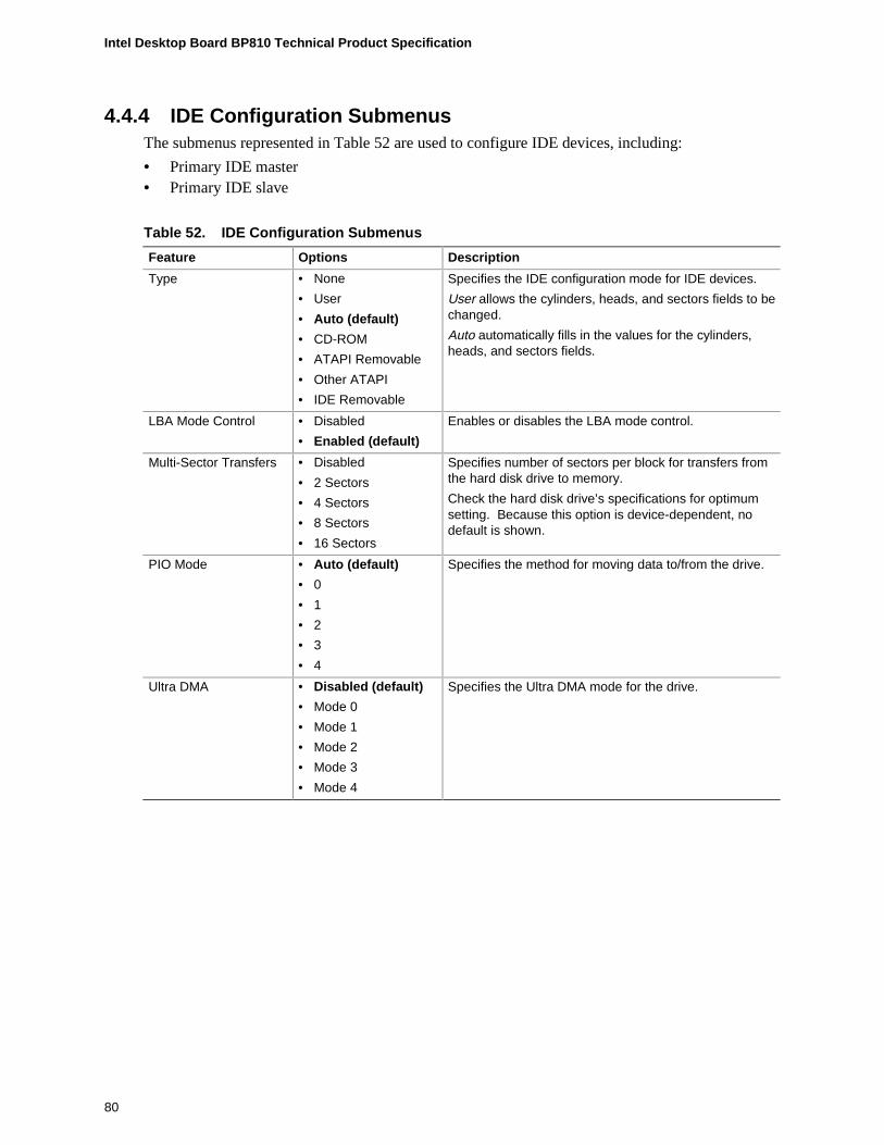
Intel Desktop Board BP810 Technical Product Specification
80
4.4.4 IDE Configuration SubmenusThe submenus represented in Table 52 are used to configure IDE devices, including:
• Primary IDE master• Primary IDE slave
Table 52. IDE Configuration Submenus
Feature Options Description
Type • None
• User
• Auto (default)
• CD-ROM
• ATAPI Removable
• Other ATAPI
• IDE Removable
Specifies the IDE configuration mode for IDE devices.
User allows the cylinders, heads, and sectors fields to bechanged.
Auto automatically fills in the values for the cylinders,heads, and sectors fields.
LBA Mode Control • Disabled
• Enabled (default)
Enables or disables the LBA mode control.
Multi-Sector Transfers • Disabled
• 2 Sectors
• 4 Sectors
• 8 Sectors
• 16 Sectors
Specifies number of sectors per block for transfers fromthe hard disk drive to memory.
Check the hard disk drive’s specifications for optimumsetting. Because this option is device-dependent, nodefault is shown.
PIO Mode • Auto (default)
• 0
• 1
• 2
• 3
• 4
Specifies the method for moving data to/from the drive.
Ultra DMA • Disabled (default)
• Mode 0
• Mode 1
• Mode 2
• Mode 3
• Mode 4
Specifies the Ultra DMA mode for the drive.

BIOS Setup Program
81
4.4.5 Diskette Configurations SubmenuThe submenu represented by Table 53 is used for configuring the diskette drive.
Table 53. Diskette Configurations Submenu
Feature Options Description
Diskette Controller • Disabled
• Enabled (default)
Disables or enables the integrated diskettecontroller.
Diskette A • Not Installed
• 360 KB 5¼ "
• 1.2 MB 5¼ "
• 720 KB 3½ "
• 1.44/1.25 MB 3½ " (default)
• 2.88 MB 3½ "
Specifies the capacity and physical size ofdiskette drive A.
Diskette Write Protect • Disabled (default)
• Enabled
Disables or enables write protect for thediskette drive.
4.4.6 Event Log ConfigurationThe submenu represented by Table 54 is used to configure the event logging features.
Table 54. Event Log Configuration Submenu
Feature Options Description
Event log No options Indicates if there is space available in the event log.
Event log validity No options Indicates if the contents of the event log are valid.
View event log [Enter] Displays the event log.
Clear all event logs • No (default)
• Yes
Clears the event log after rebooting.
Event Logging • Disabled
• Enabled (default)
Enables logging of events.
Mark events as read [Enter] Marks all events as read.
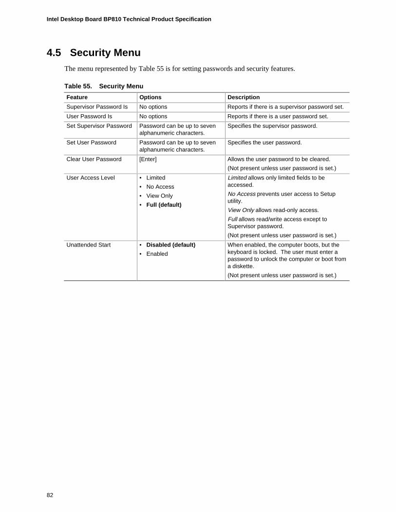
Intel Desktop Board BP810 Technical Product Specification
82
4.5 Security MenuThe menu represented by Table 55 is for setting passwords and security features.
Table 55. Security Menu
Feature Options Description
Supervisor Password Is No options Reports if there is a supervisor password set.
User Password Is No options Reports if there is a user password set.
Set Supervisor Password Password can be up to sevenalphanumeric characters.
Specifies the supervisor password.
Set User Password Password can be up to sevenalphanumeric characters.
Specifies the user password.
Clear User Password [Enter] Allows the user password to be cleared.
(Not present unless user password is set.)
User Access Level • Limited
• No Access
• View Only
• Full (default)
Limited allows only limited fields to beaccessed.
No Access prevents user access to Setuputility.
View Only allows read-only access.
Full allows read/write access except toSupervisor password.
(Not present unless user password is set.)
Unattended Start • Disabled (default)
• Enabled
When enabled, the computer boots, but thekeyboard is locked. The user must enter apassword to unlock the computer or boot froma diskette.
(Not present unless user password is set.)

BIOS Setup Program
83
4.6 Boot MenuThe menu represented in Table 56 is used to set the boot features and the boot sequence.
Table 56. Boot Menu
Feature Options Description
Quiet Boot • Disabled
• Enabled (default)
Disabled displays normal POST messages.
Enabled displays OEM logo instead of POSTmessages.
Quick Boot • Disabled
• Enabled (default)
Enables the computer to boot without running certainPOST tests.
Scan User FlashArea
• Disabled (default)
• Enabled
Enables the BIOS to scan the flash memory for userbinary files that are executed at boot time.
After Power Failure • Stays Off
• Last State (default)
• Power On
Specifies the mode of operation if an AC/Power lossoccurs.Power On restores power to the computer.
Stay Off keeps the power off until the power button ispressed.
Last State restores the previous power state beforepower loss occurred.
First Boot Device
Second Boot Device
Third Boot Device
Fourth Boot Device
• Floppy
• ARMD-FDD (Note 1)
• ARMD-HDD (Note 2)
• IDE-HDD (Note 3)
• ATAPI CDROM
• Disabled
Specifies the boot sequence from the available devices.To specify boot sequence:
1. Select the boot device with <↑> or <↓>.
2. Press <Enter> to set the selection as the intendedboot device.
The operating system assigns a drive letter to eachboot device in the order listed. Changing the order ofthe devices changes the drive lettering.
Not all of the devices in this list are available as second,third, and fourth boot devices. The default settings forthe first through fourth boot devices are, respectively:
• Floppy
• IDE-HDD
• ATAPI CDROM
• Disabled
IDE DriveConfiguration
• Primary Master IDE 1st IDE (default)
• Primary Slave IDE 2nd IDE
Selects the IDE boot device. If selected, allows theslave IDE device to be the boot device.
Notes:
1. ARMD-FDD = ATAPI removable device - floppy disk drive
2. ARMD-HDD = ATAPI removable device - hard disk drive
3. HDD = Hard Disk Drive

Intel Desktop Board BP810 Technical Product Specification
84
4.7 Exit MenuThe menu represented in Table 57 is for exiting the BIOS Setup program, saving changes, andloading and saving defaults.
Table 57. Exit Menu
Feature Description
Exit Saving Changes Exits and saves the changes in CMOS SRAM.
Exit Discarding Changes Exits without saving any changes made in the BIOS Setup program.
Load Setup Defaults Loads the factory default values for all the Setup options.
Load Custom Defaults Loads the custom defaults for Setup options.
Save Custom Defaults Saves the current values as custom defaults. Normally, the BIOS reads theSetup values from flash memory. If this memory is corrupted, the BIOS reads thecustom defaults. If no custom defaults are set, the BIOS reads the factorydefaults.
Discard Changes Discards changes without exiting Setup. The option values present when thecomputer was turned on are used.

85
5 Error Messages and Beep Codes
What This Chapter Contains5.1 BIOS Error Messages................................................................................................ 855.2 Bus Initialization Checkpoints .................................................................................... 875.3 Speaker ..................................................................................................................... 885.4 BIOS Beep Codes ..................................................................................................... 89
5.1 BIOS Error MessagesTable 58 lists the error messages and provides a brief description of each.
Table 58. BIOS Error Messages
Error Message Explanation
GA20 Error An error occurred with Gate-A20 when switching to protectedmode during the memory test.
Pri Master HDD ErrorPri Slave HDD Error
Could not read sector from corresponding drive.
Pri Master Drive - ATAPI IncompatiblePri Slave Drive - ATAPI Incompatible
Corresponding drive in not an ATAPI device. Run Setup to makesure device is selected correctly.
A: Drive Error No response from diskette drive.
Cache Memory Bad An error occurred when testing L2 cache. Cache memory may bebad.
CMOS Battery Low The battery may be losing power. Replace the battery soon.
CMOS Display Type Wrong The display type is different than what has been stored in CMOS.Check Setup to make sure type is correct.
CMOS Checksum Bad The CMOS checksum is incorrect. CMOS memory may havebeen corrupted. Run Setup to reset values.
CMOS Settings Wrong CMOS values are not the same as the last boot. These valueshave either been corrupted or the battery has failed.
CMOS Date/Time Not Set The time and/or date values stored in CMOS are invalid. RunSetup to set correct values.
DMA Error Error during read/write test of DMA controller.
FDC Failure Error occurred trying to access diskette drive controller.
HDC Failure Error occurred trying to access hard disk controller.
continued

Intel Desktop Board BP810 Technical Product Specification
86
Table 58. BIOS Error Messages (continued)
Error Message Explanation
Checking NVRAM..... NVRAM is being checked to see if it is valid.
Update OK! NVRAM was invalid and has been updated.
Updated Failed NVRAM was invalid but was unable to be updated.
Keyboard Is Locked The system keyboard lock is engaged. The system must beunlocked to continue to boot.
Keyboard Error Error in the keyboard connection. Make sure keyboard isconnected properly.
KB/Interface Error Keyboard interface test failed.
Memory Size Decreased Memory size has decreased since the last boot. If no memory wasremoved then memory may be bad.
Memory Size Increased Memory size has increased since the last boot. If no memory wasadded there may be a problem with the system.
Memory Size Changed Memory size has changed since the last boot. If no memory wasadded or removed then memory may be bad.
No Boot Device Available System did not find a device to boot.
Off Board Parity Error A parity error occurred on an offboard card. This error is followedby an address.
On Board Parity Error A parity error occurred in onboard memory. This error is followedby an address.
Parity Error A parity error occurred in onboard memory at an unknownaddress.
NVRAM / CMOS / PASSWORD clearedby Jumper
NVRAM, CMOS, and passwords have been cleared. The systemshould be powered down and the jumper removed.
<CTRL_N> Pressed CMOS is ignored and NVRAM is cleared. User must enter Setup.

Error Messages and Beep Codes
87
5.2 Bus Initialization CheckpointsThe system BIOS gives control to the different buses at several checkpoints to do various tasks.Table 59 describes the bus initialization checkpoints.
Table 59. Bus Initialization Checkpoints
Checkpoint Description
2A Different buses init (system, static, and output devices) to start if present.
38 Different buses init (input, IPL, and general devices) to start if present.
39 Display different buses initialization error messages.
95 Init of different buses optional ROMs from C800 to start.
While control is inside the different bus routines, additional checkpoints are output to port 80h asWORD to identify the routines under execution. In these WORD checkpoints, the low byte of thecheckpoint is the system BIOS checkpoint from which the control is passed to the different busroutines. The high byte of the checkpoint is the indication of which routine is being executed in thedifferent buses. Table 60 describes the upper nibble of the high byte and indicates the function thatis being executed.
Table 60. Upper Nibble High Byte Functions
Value Description
0 func#0, disable all devices on the bus concerned.
1 func#1, static devices init on the bus concerned.
2 func#2, output device init on the bus concerned.
3 func#3, input device init on the bus concerned.
4 func#4, IPL device init on the bus concerned.
5 func#5, general device init on the bus concerned.
6 func#6, error reporting for the bus concerned.
7 func#7, add-on ROM init for all buses.

Intel Desktop Board BP810 Technical Product Specification
88
Table 61 describes the lower nibble of the high byte and indicates the bus on which the routines arebeing executed.
Table 61. Lower Nibble High Byte Functions
Value Description
0 Generic DIM (Device Initialization Manager)
1 Onboard system devices
2 ISA devices
3 EISA devices
4 ISA PnP devices
5 PCI devices
5.3 SpeakerA 47 Ω inductive speaker is mounted on the board. The speaker provides audible error code (beepcode) information during the power-on self-test (POST).
For information about Refer to
The location of the onboard speaker Figure 1, page 14
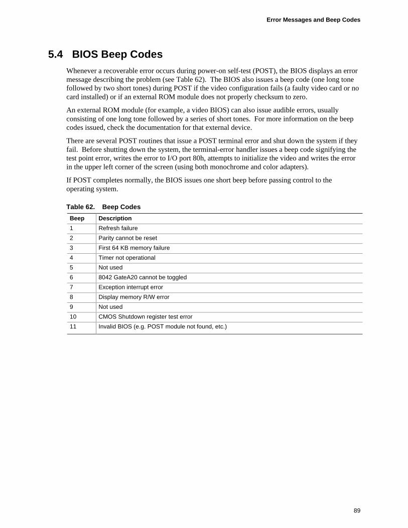
Error Messages and Beep Codes
89
5.4 BIOS Beep CodesWhenever a recoverable error occurs during power-on self-test (POST), the BIOS displays an errormessage describing the problem (see Table 62). The BIOS also issues a beep code (one long tonefollowed by two short tones) during POST if the video configuration fails (a faulty video card or nocard installed) or if an external ROM module does not properly checksum to zero.
An external ROM module (for example, a video BIOS) can also issue audible errors, usuallyconsisting of one long tone followed by a series of short tones. For more information on the beepcodes issued, check the documentation for that external device.
There are several POST routines that issue a POST terminal error and shut down the system if theyfail. Before shutting down the system, the terminal-error handler issues a beep code signifying thetest point error, writes the error to I/O port 80h, attempts to initialize the video and writes the errorin the upper left corner of the screen (using both monochrome and color adapters).
If POST completes normally, the BIOS issues one short beep before passing control to theoperating system.
Table 62. Beep Codes
Beep Description
1 Refresh failure
2 Parity cannot be reset
3 First 64 KB memory failure
4 Timer not operational
5 Not used
6 8042 GateA20 cannot be toggled
7 Exception interrupt error
8 Display memory R/W error
9 Not used
10 CMOS Shutdown register test error
11 Invalid BIOS (e.g. POST module not found, etc.)

Intel Desktop Board BP810 Technical Product Specification
90
5.5 Enhanced Diagnostic LEDs (Optional)The enhanced diagnostics feature consists of a hardware decoder and four LEDs located betweenthe RJ-45 LAN connector and the audio connectors on the back panel. This feature requires nomodifications to the chassis (other than I/O back panel shield) or cabling.
Figure 15 shows the location of the diagnostics LEDs. Table 63 lists the diagnostics codesdisplayed by the LEDs.
OM08678
1
4
Figure 15. Enhanced Diagnostics LEDs

Error Messages and Beep Codes
91
Table 63. Enhanced Diagnostics Codes
Display BIOS Operation Display BIOS OperationAmberAmberAmberAmber
Power on, starting BIOS GreenAmberAmberAmber
Undefined
AmberAmberAmberGreen
Recovery mode GreenAmberAmberGreen
Undefined
AmberAmberGreenAmber
Processor, cache, etc. GreenAmberGreenAmber
Undefined
AmberAmberGreenGreen
Memory, autosize, shadow, etc. GreenAmberGreenGreen
Undefined
AmberGreenAmberAmber
PCI bus initialization GreenGreenAmberAmber
Undefined
AmberGreenAmberGreen
Video GreenGreenAmberGreen
Undefined
AmberGreenGreenAmber
IDE bus initialization GreenGreenGreenAmber
Reserved
AmberGreenGreenGreen
USB initialization GreenGreenGreenGreen
Booting operating system

Intel Desktop Board BP810 Technical Product Specification
92