INTEGRATED CIRCUIT STANDARDIZATION WITHIN DEFENSE …
19
INTEGRATED CIRCUIT STANDARDIZATION WITHIN DEFENSE SYSTEMS DIVISION by R. J. Kerler St. Paul Transactions of the Fourth UNIVAC Engineering Symposium 1965
Transcript of INTEGRATED CIRCUIT STANDARDIZATION WITHIN DEFENSE …
INTEGRATED CIRCUIT STANDARDIZATION WITHIN DEFENSE SYSTEMS DIVISION
b y
R. J. Kerler
St. Paul
Transactions of the Fourth UNIVAC Engineering Symposium
1965

The potential improvements in size, power, performance, reliability, andcost available with semiconductor integrated circuits have received a great dealattention throughout the electronic industry. From the start, digital switch-ing applications have received the major benefit from this new technology,due to process requirements well within the state-of-the-art and also due tothe large number of repetitive functions inherent in most digital machines.Continuing its leadership in the application of new techniques, the UNIVACDefense Operations in St. Paul was one of the first systems manufacturers inthe United States to actively investigate and use integrated circuits. Thepurpose of this paper is to summarize the growth of this field within Defenseand to discuss in detail progress during the last 12 months toward a "Standard"integrated circuit family fulfilling the earlier mentioned promises.
The first significant step taken by Defense was a development contractwith Sperry Semiconductor as part of the ADD program. This effort during1960-61 proved to be premature but did form a basis for future planning andfunding. An engineering group was set up to centralize our activities during1962 but it was not until early 1963 that major emphasis was placed on theentire microelectronics field. At that time the decision was made to becomea major factor in the Aerospace business and an entire department was organizedto handle this work. The 1824 computer used on such programs as MMRBM, BGRV,MBRV, and SABRE required the design of the first integrated circuit familyused in UNIVAC. The circuits were packaged in a 10 pin -k x -t inch flat pakwhich was the industry standard at that time. An extensive vendor evaluationwas conducted before Westinghouse and Signetics were selected as the primarysources. Although active work on the circuits started during the Spring of1963, they are still in volume use today with only minor modifications. The16 circuits comprising the family consist of six logic, eight memory, andtwo I/0 circuits. The characteristics of the six logic circuits involved areshown in Figure 1. This family was designed with minimum part count, minimumpower, maximum noise margin, and maximum reliability as primary considerations.This resulted in a compromise on type count, speed, and cost although theearly date of this development must be remembered in comparison to recentperformance and process improvements.
Characteristic "1824n
1. Package 10 Lead Flat Pak2. Fanout 53. Collector Logic Capability No4. Operating Temperature 00 to +125°C5. Power Per Inverter (Avg.) 5 MW6. Noise Margin (Minimum) .5V7. Supply Voltages 4V8. Propagation Speed (Typ.) 50 NS
FIGURE 1
During late 1962 a contract was negotiated with the Department of Navy for thelarge scale high speed CP-667 system. Due to speed and availability considera-tions, the decision was made to develop a hybrid chip circuit rather than amonolithic fully integrated device. At that time, Motorola was the leadingproponent of hybrid devices and also the number one supplier of semiconductordevices to UNIVAC. A development program was started during the Winter of1962-63 requiring four logic diode types, one dual transistor gate, and threememory diode types. Each of the types was packaged in a low silhouette 10pin TO 5 package. Military certified devices were delivered during 1963and 1964 which satisfactorily met the electrical specifications but whichsubsequently developed a serious failure mode during the system qualificationtest. A photograph of the internal construction of a typical chip circuit is

FIGURE 2
-2-
shown in Figure 2. The thermo-compression bonding technique(stitch bonding) used to attachthe one mil aluminum internalwires to the active or resistivechips and to the bonding pads,was proved to be less reliablethan other bonding techniques andsubject to extreme process varia-tions. Although the percentageof devices which failed in thecomputer was quite low (0.1% orless) the complexity of themachine and its environmentalrequirements required a failurerate much closer to zero.
It was at this point thatthe reliability advantagesinherent in silicon monolithicintegrated circuits, and therapidly improving performanceavailable using this techniquebecame attractive. A study conductedby UNIVAC had concluded in Augustof 1964 that the performancerequired for the CP-667 systemwas attainable with fullyintegrated technology andthat the major failure modeof the chip circuits was signifi-cantly reduced with monolithics. Although a limited development program hadbeen started early in 1964 to obtain monolithic circuits for this application,the effort was expanded in November of 1964 through the cooperative effortsof Reliability, Design Engineering, and Purchasing personnel. This work waspartially sponsored by the Bureau of Ships with the ground rule that printedcircuit cards using monolithics perform the same functions and be inter-changeable with cards using hybrid circuits.
Originally it was felt that three variations of the basic circuit shouldbe developed: a dual four input gate, a triple gate having 2, 3, and 4 inputs,respectively, and a quad, two input gate. In addition, the possibility of
CIRCUIT COUNT FOR CP-667 CENTRAL PROCESSOR
3-3 and 2-4 4-4 4-3-2 4-4 and 2-2-2-2 4-4 and 4-3-2 and 2-2-2-210 Pin 14 Pin 14 Pin 14 Pin 14 Pin 12K 11K 9K 7K 6K
FIGURE 3
using the master slice approach was considered. This would have meant one setof masks for all three circuit types, except for the final metalization masks.Due to the potential volume predicted for 1966 and beyond, most of the vendorspreferred to optimize each set of masks and each chip size for the specific circuitinvolved. Figure 3 shows the approximate number of circuits required in a
-3-
667 central processor for various combinations of the circuits. Since keep-ing the number of circuit types to a minimum was considered an importantgoal, the dual and quad gates were selected for development. It was feltthat the triple gate could be obtained on a short turn around development atsome future date if a real need was shown.
Every semiconductor vendor known to have capability in the integratedcircuit field was given an opportunity to participate in the early phasesof the pre-contract negotiations. Purchase part drawings had been writtenearlier so there were no last minute changes in scope or direction. Sevenvendors indicated a desire to work with UNIVAC on the shared cost develop-ment program. The final selection of five vendors was based on past performance,long range projected pricing, vendor interest in participating, and our judg-ment on their capabilities. Purchase orders were placed with each of the fivevendors during the first week in December of 1964. The orders defined expecteddelivery-date, process monitoring requirements, the necessity for semimonthlystatus reports, milestone dates that the vendors progress would be chartedagainst, termination provisions, and UNIVAC's qualification criteria.
Although an equivalent circuit was shown on the purchase part drawingsfor guidance, the vendors were allowed to use any technique which would meetthe electrical requirements. The various configurations submitted by thethree vendors actually delivering parts are shown in Figure 4. The multipleemitter input transistor used by Signetics with the promise of higher speeds,unfortunately, had a reduced noise margin when compared to the normal inputdiodes used on the Westinghouse and Motorola chips. It subsequently becameobvious that the only way for Signetics to correct this problem would be tocompletely redesign their masks. The early problems which Motorola encounteredwere apparently due to their reluctance to use the buried layer techniquefor reducing collector resistance and capacitance. A brief summary of ourexperiences with each of the five vendors is shown in Figure 5. A review ofthis summary indicates that Westinghouse has performed quite well, Motorolajust recently demonstrated its capability to meet our requirements, Signeticsdelivered samples but could never meet all of the drawing requirements, andTI and Fairchild never produced electrically good units.
It is rather interesting to review photomicrographs of representativechips submitted by the two successful vendors. Figure 6 shows a Westinghousedual gate (7901000) using a 50 x 52 mil chip with aluminum metalization andone mil ball bonded gold wire. Although this chip is very well laid out,several disadvantages exist. Two extra wires and bonds are required to getfrom the ground pads on the chip to the single external ground lead. Thistechnique also has the undesirable feature of bonding to a surface which isbelow the top surface of the chip. Another questionable area involves thesupply voltage tunnel under the metalization between the two offset diodes andthe base of the output transistors, and under the ground metalization.Additional wires and bonds and resistive tunnels are generally avoided unlessabsolutely necessary. Another method of handling this circuit is shown inFigure 7. This Motorola dual gate uses a 49 x 49 mil chip with aluminummetalization and one mil stitch bonded aluminum wire. In this case Motorola'sceramic package does not allow bonding ground leads to the package so theyhave increased the amount of metalization required for the ground connectionand relied on a single wire to tie to the external ground lead. Note alsothe rather large area storage diode used as a speed-up capacitor across the
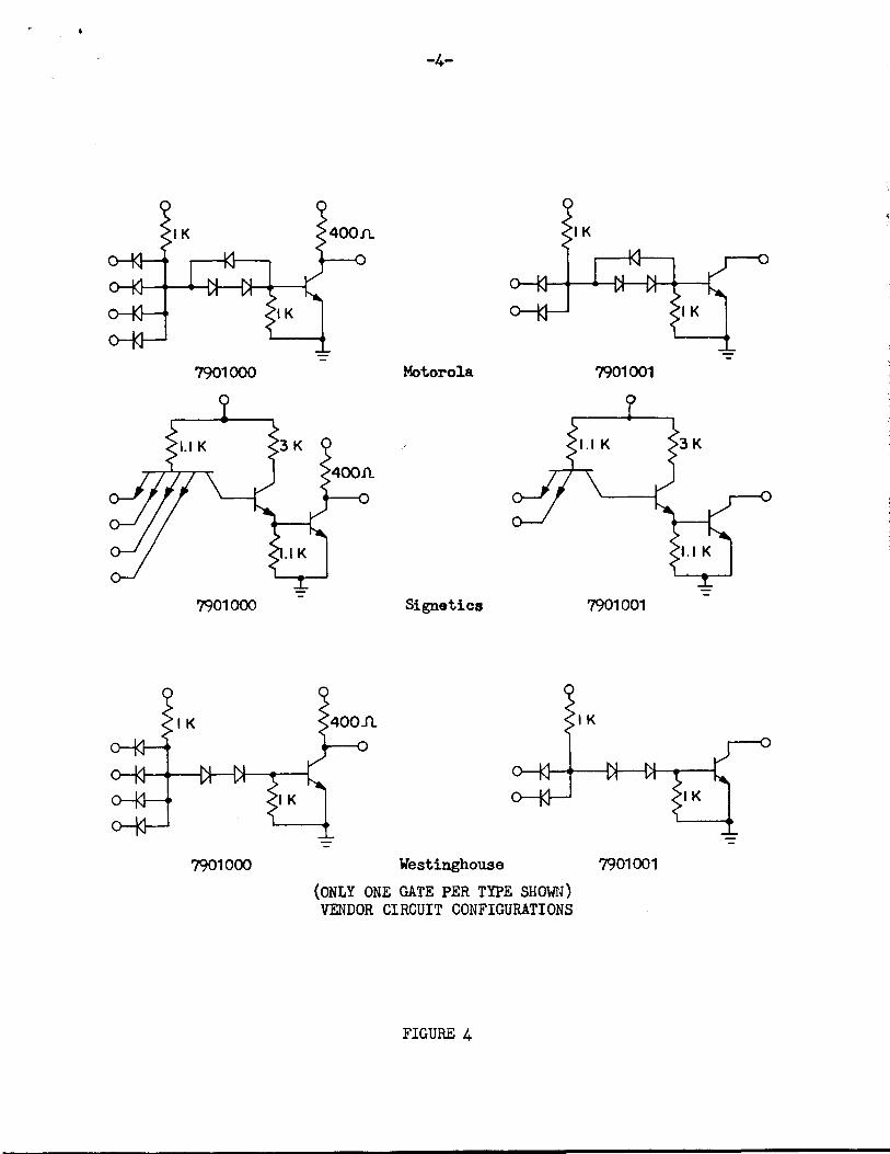
7901000 7901001Signetics
7901000 Motorola 7901001
7901000
Westinghouse 7901001
(ONLY ONE GATE PER TYPE SHOWN)VENDOR CIRCUIT CONFIGURATIONS
FIGURE 4

-5-
NOTE: All initial development orders placed during December 1965.
Vendor Status
1. Fairchild Cancelled 17 March 1965. Unacceptableelectrical design. Very large speed-upcapacitors.
2. Signetics Marginal prototypes delivered duringMarch 1965. Partial cancellation 26 May1965 due to inability to show futurecapability to meet specifications.
3. Texas Instruments Partial cancellation 12 April 1965.Inability to deliver electrically goodunits.
4. Motorola Marginal prototypes delivered from Marchthrough June 1965. Acceptable prototypesdelivered in September 1965.
5. Westinghouse Acceptable duals delivered during March1965. Acceptable quads delivered duringApril 1965. Majority of order deliveredduring May and June 1965.
FIGURE 5
offset diodes. The quad gate (7901001) which requires more individual componentsis a more striking example of the differences between the two manufacturers.Figure 8 shows a Westinghouse quad gate with two inputs per gate using a 51 x 60mil chip. This is a very clean chip considering its complexity but again multipleground leads (this time four from the chip to the case and one from the caseto the external lead wire) and two supply voltage tunnels are required. Comparethis to Figure 9 showing the Motorola quad gate on a 55 x 55 mil chip. Motorolais required to use a wide metalization path which surrounds 3/4 of the activearea. When the long path used for the supply voltage metalization is included,it means that 10 of the 14 lead wires cross over metalization at some othervoltage potential and that each is longer than normally required. Note againthe four large storage diodes along a line through the center of the chip.It should be quite obvious that the optimum layout of a complex high performancemonolithic chip involves trial and error, followed by compromise.
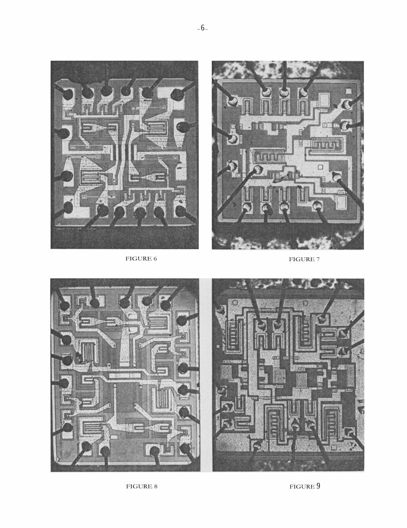
FIGURE 6 FIGURE 7
-6-
FIGURE 8 FIGURE 9

-7-
Since one of the major reasons for funding a custom design on this circuitfamily involved the need for a very fast logic circuit, it is important todiscuss the test data which has been accumulated. As mentioned earlier,experienced engineers from both the Reliability and Design Engineering groupsworked together on all phases of this development. The data taken was gatheredby both of these groups. Figure 10 lists the nominal operating conditions forthese two circuits. It is at this point that the major advantages and dis-advantages of this circuit family should be apparent. The major advantagesinvolve very high speed, high noise immunity over the entire MIL temperaturerange, the ability to perform collector logic (allowing two levels of logic to
Characteristic "7901000"
1. Package 14 Lead Flat Pack2. Fanout 63. Collector Logic Capability Yes4. Operating Temperature -55°C to +1250C5. Power Per Inverter (Avg.) 30 NW6. Noise Margin (Minimum) .35 V7. Supply Voltages 6 V and 3 V8. Propagation Speed (Typ.) 10 NS
FIGURE 10
be performed in one propagation time) and potential low cost due to the straightforward layout possible. The primary disadvantage of the family is centeredaround the relatively high power dissipated in each gate. While power dissipa-tion is critically important in most deep space and aerospace work, otherconsiderations are more important for avionics, ground, and commercial applica-tions. It is in these areas that this logic circuit is intended to excel.Because propagation times are normally given first consideration, Figure 11plots a typical circuit under minimum and maximum loading at various supplyvoltages, against ambient temperature. Although the propagation times are quitelow over most of the operating range, a storage phenomenon is evident at thehighest supply voltage and operating temperature. Although this combination ofconditions is not present in any of the systems now under consideration for thesecircuits, we are spending a great deal of time on this problem. It appearslikely after lengthy discussions with our suppliers that process control offersthe most promising solution. Process improvements that eliminate this storageeffect at the voltage and temperature extremes, will also offer better controland possible improvement at normal operating conditions. A comparison betweenthe propagation delay times under minimum and maximum loading for the basic logicgates used in our two preferred integrated circuit families (7901000 and 7900310)is shown in Figure 12. As explained earlier, the 7901000 originally developedfor 667 was designed for maximum speed with dissipation a secondary considera-tion. The 7900310, on the other hand, stresses low dissipation at moderatespeeds optimizing it for the 1824 aerospace computer.
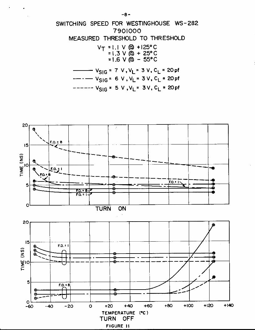
-8-SWITCHING SPEED FOR WESTINGHOUSE WS- 282
7901000MEASURED THRESHOLD TO THRESHOLD
VT =1.1 V ft +125°C=1.3V ft + 25° C=1.6 V ft - 55°C
VSIG 7 V ,VL = 3 V, C L = 20pf
VSIG 6 V Vl_' 3V , CL 20Pf
VSIG
.., F.O. 5 8-4
■ ....................- -..-...... ...... -...-- - ....._ _ _ -....,. .
\F..8
..‹..........
8
...
-- _______
..11■0. F.O.= I
=
--_-__„,
–0
49
1-4)'-4/0
0
F.O.= 8-Ar oF.O. = I o
TURN ON
o F.O.0
_= I
a .0„,„11
•
F.O. Z 8 .0,. ....,.- --
.."0
e---- -0
-60 -40 -20 0 +20 +40 +60
TEMPERATURE (•CTURN OFF
FIGURE II
20
15
U)zW 102I-
5
20
5 V ,VL = 3V, CL = 20pf
15
zWI0I-
5
0+100
+120
+140

-co2
217:
80
0
- 9 -
SWITCHING SPEED FOR WESTINGHOUSE7900310 AND 7901000
MEASURED THRESHOLD TO THRESHOLDNOMINAL OPERATING CHARACTERISTICS
7900310 7901000VS = 4V VS1G= 6 VCL = 50pf. VS = 3 V
CL = 20 pf.
THE 7900310 IS SPECIFIED TO OPERATE FROM 0°C TO +125°C,WHILE THE 7901000 IS SPECIFIED TO OPERATE OVER THEFULL TEMPERATURE RANGE OF -55°C TO +125° C .
790
f.0-'
F .O.z % ---- ' --- - -
-- ,_...
-
_ -
---.-- Fa ') 7901000 F.0.=8FA= 8
____,____ . -L.F.O. : 1TURN ON
60
cn
w 42F-
20
10
0
'..0
7900310
.... — -- --•- --
----4.—_---•- - - -
F.O.: 5F.O.: % -
_- - - -
- -- - - _-_ - .
- - - - - - - -
4.--._ _ FO z 1 7901000
, ---7
FO. : 8 __,_____n „____.
-60 -40 -20 0 +20 -1-40 +60
+80
4-100 4-120 +140
TEMPERATURE (°C)TURN OFFFIGURE 12

p
1WESTINGHOUSE MOTOROLA
1/4" X 1/4" 0.350" DIAFLAT PAK 10 LEAD•TO-5
KOVAR PACKAGE KOVAR CANCERAMIC HEADER
—10—
A major consideration involved in the application of integrated circuitsinvolves the selection of the package. In order to better understand the var-ious integrated, circuit packages which are being used at present, note therelative sizes shown in Figure 13. All four of the small flat packages (usingribbon leads on 50 mil centers) are being used interchangeably by St. PaulDefense while the larger package (with stiff leads on 100 mil centers) for plug-in applications is under development for Blue Bell commercial machines. Since
FAIRCHILDI /4 "X 3 /4 "
DUAL IN LINEPACKAGE
AU_ CERAMIC
MOTOROLAI/4" X 1/4"FLAT PAK
ALL CERAMIC
SIGNETICS1/4" X 3/8"FLAT PAKKOVAR LID
GLASS PACKAGE
T. I.
1/4"X I/8'sFLAT PAK
KOVAR PACKAGE
FIGURE 13
virtually any monalithic chip currently under consideration by any of the threeUNIVAC locations can fit into any of the 14 pin packages shown, standardizationbetween locations at the chip level is being considered. Compromises are againinvolved in the selection of a preferred package similar to those discussed onchip layout. Each of the packages has its advantages and disadvantages in thefollowing areas: cost, density, hermeticity, handling and availability. It isthe writer's opinion that both basic types of packages will become industrystandards (the smaller packages have already received JEDEC approval) for present14 Pin circuit complexity. Even larger packages covering increasingly complexfunctional blocks are already being proposed for future applications.
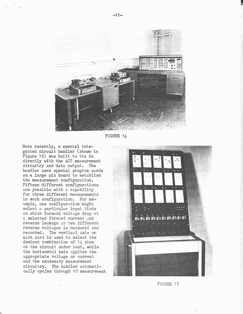
As the usage of integrated circuits increases within UNIVAC, the need foraccurate rapid measurement of each of the circuit parameters becomes increasinglyimportant. Six years ago the Test Laboratory in St. Paul designed and built alarge scale Automatic Component Tester (ACT) shown in Figure 14, for D.C. measure-ments on transistors and diodes. Because of the modular approach, extensivedata output, complete suppression of transients, and extreme accuracy availablewithin this machine, the ACT is presently being used virtually full time.
-11-
FIGURE 14
More recently, a special integrated circuit handler (shown inFigure 15) was built to tie indirectly with the ACT measurementcircuitry and data output. Thehandler uses special program cardson a large pin board to establishthe measurement configuration.Fifteen different configurationsare possible with ~ c~pability
for three different measurementsin each configuration. For example, one configuration mightselect a particular input diodeon which forward voltdge drop ata selected forward c~rent dndreverse leakage ~t two differentreverse voltages is ~easured andrecorded. The vertic~l axis one~ch card is used to select thedesired combination of 14 pinson the circuit under test, whilethe horizontal axis ~pplies theappropriate voltage or currentand the necessary ~easurement
circuitry. The handler automatically cycles through 10 measurement
FIGURE 15

-12-
sockets in sequence taking all of the programmed readings on one device and thenindexing to the next device. The handler, therefore, has a capability for a max-imum of 45 parameters on each of 10 circuits at one loading. Fourteen pin Barnessockets are used for flat paks while printed circuit connectors accept specialboards for other packages. Once the handler is started, circuits can be loadedwhile measurements continue since all pins are shorted except when a measurementis being taken. An improved handler is now under construction allowing fortwenty configurations or sixty measurements per device, and adding the desirablefeature of potential sensing using separate voltage and current probes. Whilethis arrangement is adequate for the present, significant improvements in A.C.measurement capability are needed immediately. A company funded design anddevelopment effort for such a tester is now underway. The program was startedin early 1964 but did not swing into high gear until funding became availableduring the current fiscal year.
The tester, dubbed ACMET (A.C. Microelectronic Element Tester), consists ofan automatic instrument package, a logic and input-output package, and a handler.The instrument package which is on order from Tektronix, consists of a program-mable type 567 sampling scope, a wired card programmer unit, and a programmablepulse generator. It will have the capability to take measurements between twopoints on the same wave form or from a selected point on the input wave form toa selected point on the output wave form. Each point can be established inde-pendently at a given percentage of the wave form amplitude or at a discreteinstantaneous voltage referred to ground or to a D.C. reference voltage. Thisallows it to be used to take virtually any switching or propagation time measure-ment. It also has the capability to measure D.C. voltages in much the samemanner used in taking amplitude measurements. A.C. and pulse current measurementscan be taken by installing current probes in the test circuit.
The logic control and input-output package which is being built by UNIVAC,will consist of the necessary registers and buffers and make use of standard NTDSprinted circuit cards wherever possible. Program input will be from a paper tapereader while the output will be printed on a Flexowriter. A very desirable goalbeing considered during the present hardware design stage, involves an onlineinterface with a 1218 computer. This would allow rapid calculation of distributioninformation, parameter shifts, and failure rate figures. Such a computer tie-upshould offer a significant improvement in our ability to handle large amounts ofdata without delay.
The third and most difficult portion of the tester, involves the circuithandler. This handler must provide all necessary connections between the deviceunder test and the measurement system. The handler must be capable of applyingand switching the various supply, input, and output signals with a minimum ofringing. Since many of these measurements must be made at temperature extremes,various types of pedestals, controlled gas flow, and chambers are under investi-gation. The necessity of rapid loading and unloading dictates that some type ofa carrier and feed mechanism be designed. Since the development work on thehandler is still in its early stages, the final form it will take is not known.
While the A.C. tester is receiving top priority, a new D.C. integrated cir-cuit tester having increased flexability, automatic handling, and temperatureextreme capability, is under consideration for future requirements. Although

-13—
most of the D.C. receiving-inspection testing is now done on the test lab ACT,it is anticipated that a new tester will be built or purchased for large volurreinspection purposes. The completion of the ACIET is presently planned for thesecond quarter of 1966 by which time development or delivery of the improvedD.C. inspection equipment should be in its advanced stages.
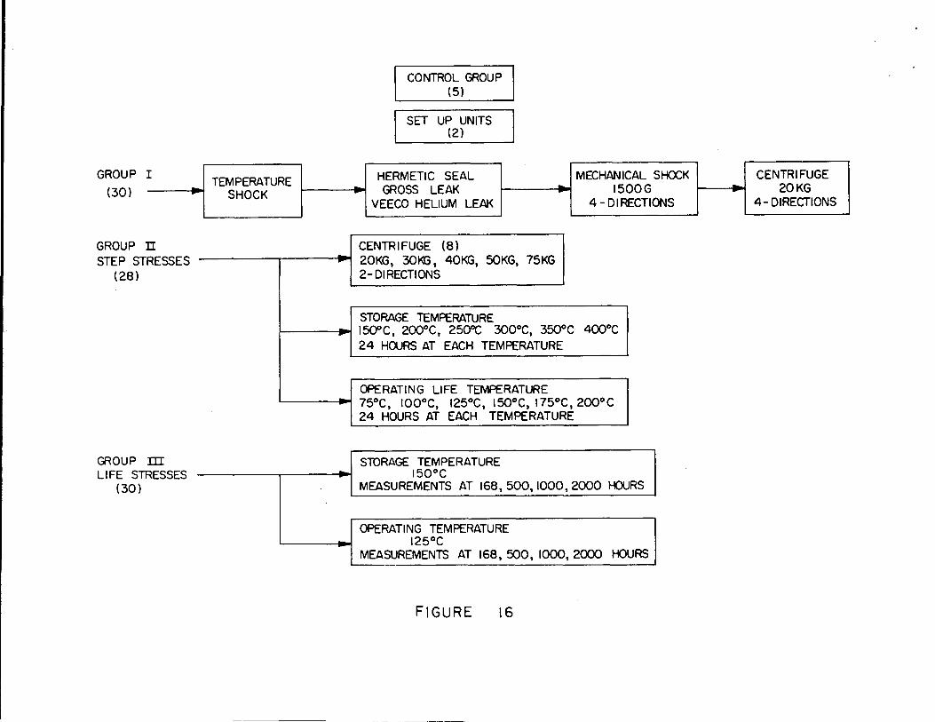
A major phase of the development program on the 7901000 circuit familyinvolves the qualification test being conducted by the Reliability Department.This test program is designed to assess the inherent reliability of these circuitsand to environmentally stress them at those mechanical and electrical stresslevels known to be indicative of adequate design margins, process controls, andworkmanship. Step stress testing is included to indicate overload capability.The test conditions and levels were selected to detect the possibility of failuremodes which have caused equipment problems with earlier discrete and partiallyintegrated semiconductors. The test program which is now in process is shown inFigure 16. A total of 100 devices of each type from each vendor are on test.The 60 units compromising Group 1 and Group III go through the normal UNIVACqualification tests used on all semiconductors except that several of the testsare run in parallel rather than sequentially. The 28 units in Group II arebeing tested to destruction on a high stress, short term step stress.
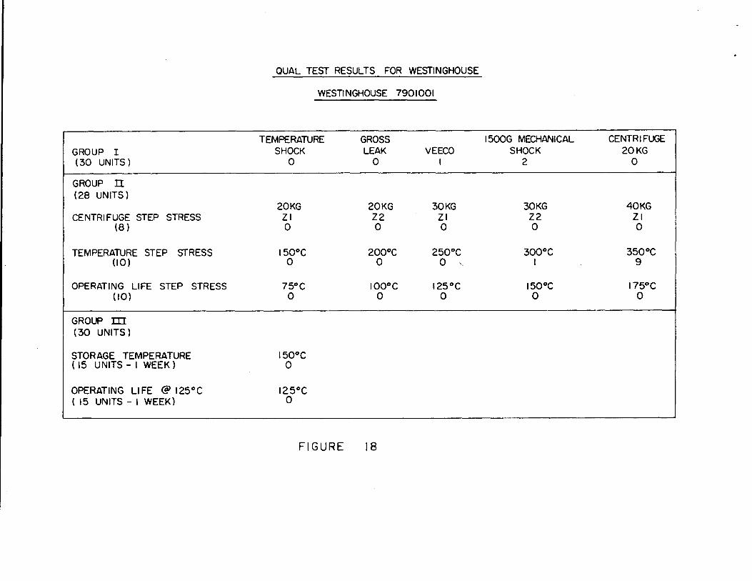
Although the qualification test is not complete, many of the tests on theWestinghouse circuits have been conducted. Figure 17 and 18 show the resultsobtained to date. Of primary concern during the early stages of the developmentprogram, was the ability of 7901001 to handle the dissipation of four gates at+125°C. The step stress results indicating no failures through +175°C ambientwhile dissipating full power, are quite encouraging. This test has been tempo-rarily interrupted while we look for a method of attaching each circuit in aring counter at ambient temperatures above 200 0C. The printed circuit boardsand soldered connections failed at 200°C although the circuits are still good.The temperature shock, hermetic seal, and mechanical tests conducted in Group Ihave looked good except for the two failure groups indicated. The single sealtest failure found during the VEECO helium leak test, is a carryover from earlierdays when package hermeticity was a serious problem. Since the measured leakrate on this unit was not excessive, the failure is not considered serious initself. The four devices failing during 1500G mechanical shock are another story.Although this test is designed to produce opens in mechanically weak units, eachof the units failed due to moderate values of leakage current which subsequentlycorrected itself several days later. These four units along with circuits fromanother test indicating a similar phenomenon, are presently included in a myster-ious failure category which is receiving a careful analysis. We are attemptingto determine whether these leakages are due to circuit weaknesses or to poor testtechniques. Since the failure corrects itself, analysis obviously is quitedifficult. The centrifuge step stress has progressed to 40,000 G without anyfailures. It is anticipated that we will go up to the maximum capability of thecentrifuge--75,000 G. The temperature step stress reached 250°C before resistanceand saturation voltage changes occurred and 300°C before catastrophic failuresoccurred. Surprisingly, two of the dual gates survived 400°C without catastrophicfailure, although the leakages and saturation voltages are much higher thanoriginally. The balance of the test sequence is now in process. Since onlylimited quantities of the Motorola circuits have been received, very little reli-ability testing has been conducted on them. It is anticipated that this testingwill start in approximately one month.
GROUP IISTEP STRESSES
(28)
CONTROL GROUP(5)
SET UP UNITS(2)
HERMETIC SEALGROSS LEAK
VEECO HELIUM LEAK
CENTRIFUGE (8)20KG, 30KG , 40KG, 50KG, 75KG2- DIRECTIONS
GROUP I
(30 )TEMPERATURE
SHOCK
MECHANICAL SHOCK
CENTRIFUGE1500 G
20 KG4 - DIRECTIONS
4- DIRECTIONS
H
STORAGE 'TEMPERATURE 150°C, 200°C, 250°C 300°C, 350°C 400°C
24 HOURS AT EACH TEMPERATURE
OPERATING LIFE TEMPERATURE 75°C, I 00°C, I25°C, I 50°C, I 75°C, 200°C
24 HOURS AT EACH TEMPERATURE
GROUP ICILIFE STRESSES
(30)
STORAGE TEMPERATUREI 50°C
MEASUREMENTS AT 168, 500,1000, 2000 HOURS
OPERATING TEMPERATUREI25°C
MEASUREMENTS AT 168, 500, 1000, 2000 HOURS
FIGURE 16
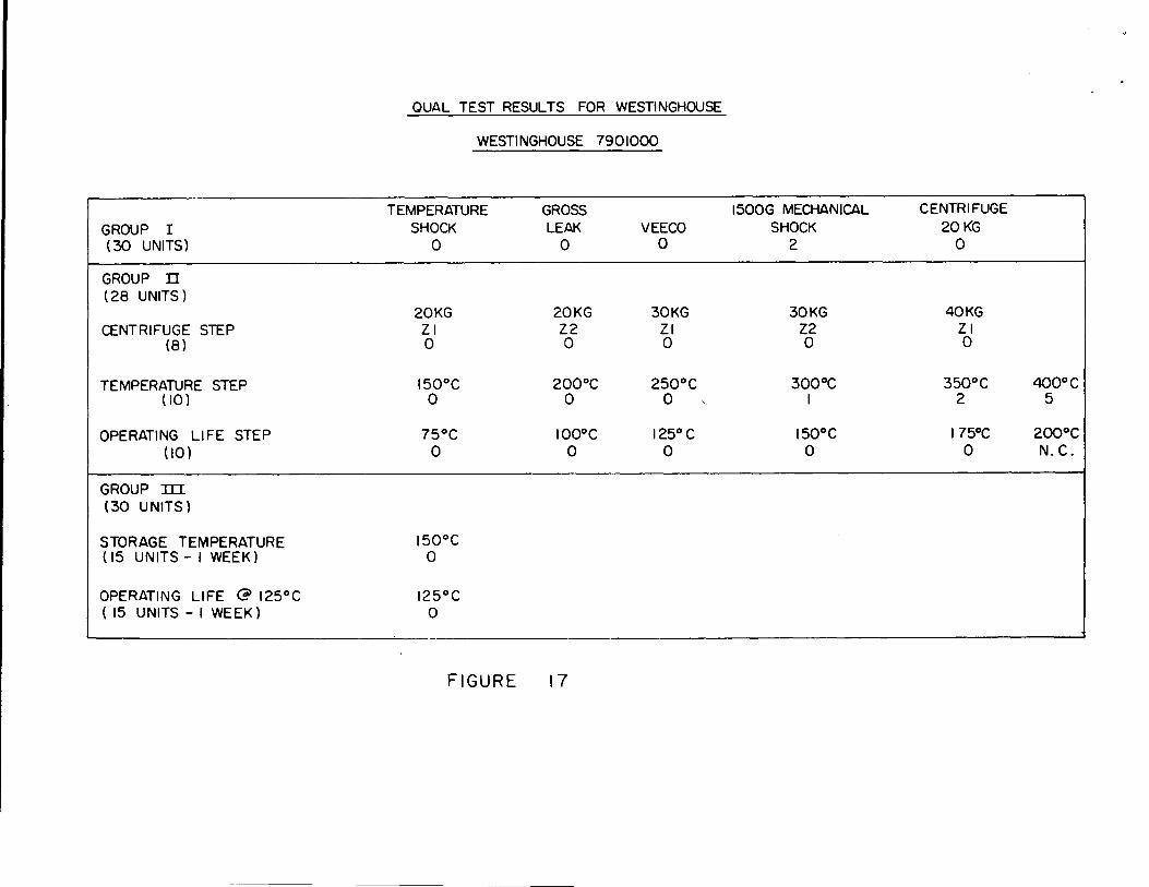
QUAL TEST RESULTS FOR WESTINGHOUSE
WESTINGHOUSE 7901000
TEMPERATURE GROSS 1500G MECHANICAL CENTRIFUGEGROUP I SHOCK LEAK V EECO SHOCK 20 KG( 30 UNITS) 0 0 0 2 0
GROUP LE(28 UNITS )
20KG 20KG 30 KG 30 KG 40 KGCENTRIFUGE STEP Z I Z2 ZI Z2 Z I
(8) 0 0 0 0 0
TEMPERATURE STEP 150°C 200°C 250°C 300°C 350°C 400°C(10) 0 0 0 2 5
OPERATING LIFE STEP 75°C 100°C 125° C 150°C 175°C 200°C(10) 0 0 0 0 0 N. C.
GROUP ICE(30 UNITS )
STORAGE TEMPERATURE(15 UNITS - 1 WEEK)
OPERATING LIFE e I25°C( 15 UNITS - I WEEK )
150°C0
125°C0
FIGURE 17
QUAL TEST RESULTS FOR WESTINGHOUSE
WESTINGHOUSE 7901001
TEMPERATURE GROSS 1500G MECHANICAL CENTRIFUGEGROUP I SHOCK LEAK V EECO SHOCK 20 KG(30 UNITS) 0 0 I 2 0
GROUP II(28 UNITS)
20KG 20KG 30 KG 30 KG 40 KGCENTRIFUGE STEP STRESS ZI Z2 ZI Z2 ZI
(8) 0 0 0 0 0
TEMPERATURE STEP STRESS I 50°C 200°C 250°C 300°C 350°C(10) 0 0 0 , I 9
OPERATING LIFE STEP STRESS 75°C I 00°C 125°C 150°C I 75°C(10) 0 0 0 0 0
GROUP m(30 UNITS )
STORAGE TEMPERATURE 150°C( 15 UNITS - 1 WEEK) 0
OPERATING LIFE @ 125°C 125°C( 15 UNITS - I WEEK) 0
FIGURE 18
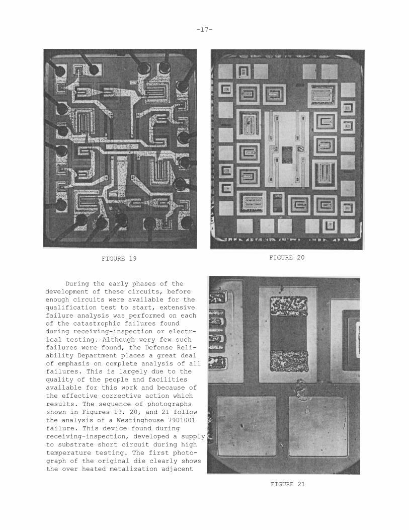
FIGURE 19 FIGURE 20
-17-
During the early phases of thedevelopment of these circuits, beforeenough circuits were available for thequalification test to start, extensivefailure analysis was performed on eachof the catastrophic failures foundduring receiving-inspection or electr-ical testing. Although very few suchfailures were found, the Defense Reli-ability Department places a great dealof emphasis on complete analysis of allfailures. This is largely due to thequality of the people and facilitiesavailable for this work and because ofthe effective corrective action whichresults. The sequence of photographsshown in Figures 19, 20, and 21 followthe analysis of a Westinghouse 7901001failure. This device found duringreceiving-inspection, developed a supplyto substrate short circuit during hightemperature testing. The first photo-graph of the original die clearly showsthe over heated metalization adjacent
FIGURE 21

-18-
to the supply voltage bond. Although the natural conclusion would be to assumethat failure was due to misuse (over voltage, wrong polarity, etc.) the secondphotograph with the bonds and aluminum metalization removed shows that the bondwas misplaced, such that it missed part of the protective bonding tub provided.The third photograph, which is a close-up of the area involved, shows that toomuch pressure apparently caused the bond to break through the protective oxidepassivating layer and short directly to the substrate. Localized heating result-ing from the point contact short, along with insufficient current limiting in thetest equipment, overheated the adjacent aluminum metalization. Althou gh thesequence of events is not absolutely established in this case, the potential forcorrective action available through complete failure analysis, should be apparent.A review of the test equipment limit circuitry was subsequently conducted atUNIVAC while the necessity of proper bond location and pressure was discussedwith the vendor.
This paper has now developed in detail, much of the planning and techniqueswhich go into the growth and final selection of a company standard integratedcircuit family. The educational period necessary to develop the necessary under-standing throughout the organization was mentioned. The engineering experimenta-tion and calculations required to justify the selection of a particular class ofcircuitry were discussed. The necessity for enthusiastic cooperation between thevarious functional groups was stressed. The close contact required between thesupplier and the user, necessary to obtain reliable high performance circuitswas pointed out. The one point which I have not previously discussed, and theone which the writer feels personally has been more important to the success ofthis program than any other, involves management understanding of the technologyinvolved and the complete support of management. While I agree with most of thepeople who are convinced of the fantastic promise of microelectronics, I amequally convinced that UNIVAC will be successful in this field only with widespread standardization actively promoted by management. Progress and profitscan be realized through well controlled, periodic updating of our circuits, butit has been well established that the cost of these circuits will be determinedprimarily by the volume per type which UNIVAC can commit at one time. Fortunatelyfor the Reliability function which I represent, low cost, high volume circuitsalso offer the potential for optimum reliability.