INTEGRATED CIRCUIT DEVICE MISMATCH MODELING … · INTEGRATED CIRCUIT DEVICE MISMATCH MODELING AND...
245
INTEGRATED CIRCUIT DEVICE MISMATCH MODELING AND CHARACTERIZATION FOR ANALOG CIRCUIT DESIGN by Patrick G. Drennan A Dissertation Presented in Partial Fulfillment of the Requirements for the Degree Doctor of Philosophy ARIZONA STATE UNIVERSITY May 1999
Transcript of INTEGRATED CIRCUIT DEVICE MISMATCH MODELING … · INTEGRATED CIRCUIT DEVICE MISMATCH MODELING AND...
INTEGRATED CIRCUIT DEVICE MISMATCH MODELING AND
CHARACTERIZATION FOR ANALOG CIRCUIT DESIGN
by
Patrick G. Drennan
A Dissertation Presented in Partial Fulfillmentof the Requirements for the Degree
Doctor of Philosophy
ARIZONA STATE UNIVERSITY
May 1999

____
____
____
____
__
__
INTEGRATED CIRCUIT DEVICE MISMATCH MODELING AND
CHARACTERIZATION FOR ANALOG CIRCUIT DESIGN
by
Patrick G. Drennan
has been approved
April 1999
APPROVED:
__________________________________________________________________, Chair
___________________________________________________________________
___________________________________________________________________
___________________________________________________________________
___________________________________________________________________
Supervisory Committee
ACCEPTED:
__________________________________
Department Chair
__________________________________
Dean, Graduate College

n of
or
d to
d
llec-
d.
oss
tched
ne
tance
the
s-
atch
t
ABSTRACT
This work presents a new method for the modeling and characterizatio
resistor, MOSFET and bipolar transistor mismatch for analog circuit design. F
transistors, sensitivities numerically calculated from SPICE models were use
infer mismatch variances in process parameters, such as sheet resistance an
geometry variation, from electrical parameter mismatch variances, such as co
tor current and drain current. For resistors, an analytical model was develope
The new models showed a significant improvement over existing models, acr
all geometries, bias conditions, temperatures and separation distances for ma
pairs.
For MOSFETs, the new model successfully fit two anomalous effects, o
caused by short channel effects and the other caused by parasitic series resis
mismatch. For bipolar transistors, a new technique for the rapid evaluation of
physical cause of BJT mismatch was developed and it was found that BJT mi
match is insensitive to temperature and collector bias. For resistors, the mism
variability depends on junction depth, ion implant dose concentration, contac
resistance, and width mismatch effects.
iii

r,
DEDICATION
This work is dedicated to my wife, Carolyn, my daughter, Amy, my mothe
Mildred, and father, Langdon.
iv

u-
lin
ul
rd
ACKNOWLEDGMENTS
I’d like to thank my dissertation committee, Dr. Dieter Schroder, Dr. Do
glas Montgomery, Dr. David Allee, Dr. Edwin Greeneich and especially Dr. Co
McAndrew for their support, consultation and advice.
I’d like to thank the many coworkers at Motorola who have helped me
through this challenging project. Specifically, I’d like to acknowledge the usef
discussions and assistance from Dr. Anoosh Abdy, Mr. John Bates, Mr. Richa
Catero, Mr. Bill Davis, Mr. Corey Gehman, Mr. Patrick Holly, Mr. Richard Ida,
Mr. Leo Kasel, Mr. Adam Kittirath, Mr. Ray Sulier, and Dr. James Victory.
v

ix
xii
1
1
1
5
8
8
1
6
19
23
31
31
42
47
50
52
54
63
TABLE OF CONTENTS
Page
LIST OF TABLES . . . . . . . . . . . . . . . . . . . . . . . . . . . . . . . . . . . . . . . . . .
LIST OF FIGURES . . . . . . . . . . . . . . . . . . . . . . . . . . . . . . . . . . . . . . . . .
CHAPTER
1 Introduction . . . . . . . . . . . . . . . . . . . . . . . . . . . . . . . . . . . . .
What is matching? . . . . . . . . . . . . . . . . . . . . . . . . . . . . . .
How is mismatch measured? . . . . . . . . . . . . . . . . . . . . . .
Outline for this thesis . . . . . . . . . . . . . . . . . . . . . . . . . . .
2 The Significance of Matching - Examples . . . . . . . . . . . . . . .
Example 1 - A BJT current mirror . . . . . . . . . . . . . . . . . .
Example 2 - A MOSFET current mirror . . . . . . . . . . . . . . 1
Example 3 - A BJT differential amplifier . . . . . . . . . . . . . 1
Example 4 - A voltage scaling DAC . . . . . . . . . . . . . . . . .
Example 5 - A band gap voltage reference. . . . . . . . . . . .
3 General Mismatch Principles . . . . . . . . . . . . . . . . . . . . . . . .
Sources of mismatch . . . . . . . . . . . . . . . . . . . . . . . . . . . .
Mismatch measures . . . . . . . . . . . . . . . . . . . . . . . . . . . . .
Propagation of Deviation and Propagation of Variance . . .
Empirical statistical modeling . . . . . . . . . . . . . . . . . . . . .
Physically based modeling . . . . . . . . . . . . . . . . . . . . . . . .
Mismatch models . . . . . . . . . . . . . . . . . . . . . . . . . . . . . . .
Mismatch experimental design. . . . . . . . . . . . . . . . . . . . .
vi

74
74
74
77
82
96
01
01
07
14
37
82
192
92
96
8
1
16
220
222
4 Resistor Mismatch . . . . . . . . . . . . . . . . . . . . . . . . . . . . . . . .
Prior work . . . . . . . . . . . . . . . . . . . . . . . . . . . . . . . . . . . .
Method . . . . . . . . . . . . . . . . . . . . . . . . . . . . . . . . . . . . . .
Test structures . . . . . . . . . . . . . . . . . . . . . . . . . . . . . . . . .
Measurements . . . . . . . . . . . . . . . . . . . . . . . . . . . . . . . . .
Mismatch of dissimilar geometries . . . . . . . . . . . . . . . . . .
5 MOSFET Mismatch . . . . . . . . . . . . . . . . . . . . . . . . . . . . . . . 1
Prior work . . . . . . . . . . . . . . . . . . . . . . . . . . . . . . . . . . . . 1
Method . . . . . . . . . . . . . . . . . . . . . . . . . . . . . . . . . . . . . . 1
A 0.8 mm Power BiCMOS Technology . . . . . . . . . . . . . . 1
A 0.28mm CMOS technology . . . . . . . . . . . . . . . . . . . . . 1
Experimental design for mismatch pairs . . . . . . . . . . . . . . 1
6 BJT Mismatch . . . . . . . . . . . . . . . . . . . . . . . . . . . . . . . . . . .
Prior work . . . . . . . . . . . . . . . . . . . . . . . . . . . . . . . . . . . . 1
Method . . . . . . . . . . . . . . . . . . . . . . . . . . . . . . . . . . . . . . 1
A vertical NPN from a 0.8mm BiCMOS technology. . . . . 19
A vertical NPN from a 1.8mm BiCMOS technology. . . . . 21
Rapid evaluation of BJT mismatch . . . . . . . . . . . . . . . . . . 2
7 Conclusions . . . . . . . . . . . . . . . . . . . . . . . . . . . . . . . . . . . . .
8 References . . . . . . . . . . . . . . . . . . . . . . . . . . . . . . . . . . . . . .
vii

16
23
28
30
82
85
92
93
99
100
115
116
LIST OF TABLES
Table Page
2.1 MOS Id mismatch for the current mirror in Figure 2.2 as afunction of current factor ratios. Note that the matching isoptimum for an area ratio of 1.0 . . . . . . . . . . . . . . . . . . . . . .
2.2 Table of variabilities due to resistor matching in the DAC ofFigure 2.4. A resistor mismatch of 1.0% was assumed forthis example . . . . . . . . . . . . . . . . . . . . . . . . . . . . . . . . . . . . .
2.3 Offset values in the reference voltage sensitivity to temperaturein the bandgap circuit in Figure 2.5. A typical 1-sigma RMMof 1.0% in R2 and R3 and 1-sigma ICMM of 0.1% in Q1 and Q2was assumed. . . . . . . . . . . . . . . . . . . . . . . . . . . . . . . . . . . . .
2.4 Optimum ratios for A1 and A2 for the Widlar bandgap voltagereference in Figure 2.5 for three different correlationcoefficients. . . . . . . . . . . . . . . . . . . . . . . . . . . . . . . . . . . . . .
4.1 Five types of resistors (A, B, C, D, and E) from a 0.8µm powerBiCMOS technology. . . . . . . . . . . . . . . . . . . . . . . . . . . . . . .
4.2 Measured versus predicted values for resistor B. . . . . . . . . . . . .
4.3 A comparison of extracted resistor mismatch parameters forthe five resistors. . . . . . . . . . . . . . . . . . . . . . . . . . . . . . . . . .
4.4 A closer evaluation of the sheet resistance mismatchcontributions for resistors A, B, and C. Note that resistors Aand B are n-type while C, D, and E are p-type. . . . . . . . . . . .
4.5 ANOVA for the dissimilar geometry analysis based on resistor A.
4.6 Extracted coefficients based on the dissimilar geometry analysis.
5.1 Geometry combinations for the 1.6µm technology nMOS andpMOS devices. . . . . . . . . . . . . . . . . . . . . . . . . . . . . . . . . . . .
5.2 Bias combinations applied to the 1.6µm nMOS device. Allpossible combinations of the listed biases were applied. . . . .
viii

117
21
122
34
134
36
136
137
138
40
41
141
42
42
158
90
190
5.3 Bias combinations applied to the 1.6µm nMOS device. Allpossible combinations of the listed biases were applied. . . . .
5.4 0.16µm technology nMOS ANOVA. . . . . . . . . . . . . . . . . . . . . . 1
5.5 Extracted nMOS mismatch model coefficients. . . . . . . . . . . . . . .
5.6 pMOS ANOVA . . . . . . . . . . . . . . . . . . . . . . . . . . . . . . . . . . . . . 1
5.7 pMOS Extracted coefficients. . . . . . . . . . . . . . . . . . . . . . . . . . . .
5.8 Combined nMOS and pMOS extraction ANOVA. . . . . . . . . . . . . 1
5.9 Comparison of nMOS and pMOS parameters. . . . . . . . . . . . . . . .
5.10 Geometry combinations for the 0.28µm technology nMOS andpMOS devices. . . . . . . . . . . . . . . . . . . . . . . . . . . . . . . . . . . .
5.11 Bias combinations applied to the 0.28µm nMOS device. Allpossible combinations of the listed biases were applied. Asimilar set of biases were applied to the pMOS but with thesigns reversed. . . . . . . . . . . . . . . . . . . . . . . . . . . . . . . . . . . .
5.12 0.28µm technology nMOS ANOVA. . . . . . . . . . . . . . . . . . . . . . 1
5.13 0.28µm technology pMOS ANOVA. . . . . . . . . . . . . . . . . . . . . . 1
5.14 nMOS and pMOS parameters before combining the fits. . . . . . . .
5.15 ANOVA for the combined nMOS and pMOS fit. . . . . . . . . . . . . 1
5.16 Comparison of nMOS and pMOS parameters with a combinednMOS and pMOS fit. . . . . . . . . . . . . . . . . . . . . . . . . . . . . . . 1
5.17 Extracted mismatch model parameters per the Pelgrom modelfor the nMOS and pMOS devices. . . . . . . . . . . . . . . . . . . . . .
5.18 A minimum list of device geometry treatment combinations (tc’s)for the MOSFET experimental design. . . . . . . . . . . . . . . . . . 1
5.19 A minimum list of measurement condition treatmentcombinations to be applied to each of the MOSFETs listedin Table 5.18. MOSFET mismatch pair is placed in a commonsource configuration. . . . . . . . . . . . . . . . . . . . . . . . . . . . . . .
ix

199
ents.
200
6.1 Geometry treatment combinations(tc) for the bipolar transistormismatch test structures. . . . . . . . . . . . . . . . . . . . . . . . . . . . .
6.2 Biasandtemperaturetreatmentcombinationsforthemismatchmeasurem199
6.3 Mismatch parameters for device A. . . . . . . . . . . . . . . . . . . . . . .
x

3
4
9
11
17
20
25
31
33
34
36
37
40
41
50
53
LIST OF FIGURES
Figure Page
1.1 A typical example of device mismatch dependence on geometry. .
1.2 A bar chart showing the number of publications on integratedcircuit device mismatch over time. . . . . . . . . . . . . . . . . . . . .
2.1 A BJT current mirror with base error in (a) and negligible baseerror in (b). . . . . . . . . . . . . . . . . . . . . . . . . . . . . . . . . . . . . . .
2.2 A MOSFET current mirror. . . . . . . . . . . . . . . . . . . . . . . . . . . . .
2.3 Two implementations of a BJT differential amplifier. . . . . . . . . .
2.4 A 3 bit voltage scaling digital to analog converter (DAC) . . . . . .
2.5 A Widlar band-gap voltage reference circuit. . . . . . . . . . . . . . . .
3.1 The components of mismatch error, from Shyu [6, 7]. . . . . . . . .
3.2 Graphical depiction of random and systematic variations. . . . . . .
3.3 A comparison of local and global mismatch errors . . . . . . . . . . .
3.4 Three depictions of radially based wafer gradients. . . . . . . . . . . .
3.5 An example of how a matched pair can be effected by athermal gradient. . . . . . . . . . . . . . . . . . . . . . . . . . . . . . . . . .
3.6 A comparison of gradients and the impact on the mismatchmean and standard deviation. . . . . . . . . . . . . . . . . . . . . . . . . .
3.7 An example of how a matched pair of resistors in (a) can becross-coupled in (b), to minimize the susceptibility togradients. . . . . . . . . . . . . . . . . . . . . . . . . . . . . . . . . . . . . . . .
3.8 A graphical depiction of Eq. (3.21) for two different functions. . .
3.9 A qualitative graph depicting the apparent lack of correlationbetween a given process parameter and an electricalparameter. . . . . . . . . . . . . . . . . . . . . . . . . . . . . . . . . . . . . . . .
xi

62
62
63
64
66
66
69
72
73
73
77
79
85
86
3.10 A plot of the experimental design (a) and predictionvariance (b) from Shyu [7]. . . . . . . . . . . . . . . . . . . . . . . . . . .
3.11 A plot of the experimental design (a) and predictionvariance (b) from Lakshmikumar [8]. . . . . . . . . . . . . . . . . . .
3.12 A plot of the experimental design (a) and predictionvariance (b) from Pelgrom [2]. . . . . . . . . . . . . . . . . . . . . . . .
3.13 Variations on matching orientation. The arrows represent the“line of matching”. . . . . . . . . . . . . . . . . . . . . . . . . . . . . . . . .
3.14 The effect of ion implantation shadowing in (b) versus a 0o
implant in (a). . . . . . . . . . . . . . . . . . . . . . . . . . . . . . . . . . . . .
3.15 Variations on device orientation. All three combinations have the same matching orientation. . . . . . . . . . . . . . . . . . . . . . . .
3.16 Plot depicts the trend of MM with device width if all devicesare placed at minimum separation distance. . . . . . . . . . . . . . .
3.17 An incomplete 32 factorial design in the inverse geometryspace. . . . . . . . . . . . . . . . . . . . . . . . . . . . . . . . . . . . . . . . . . .
3.18 A complete 32 factorial design in inverse geometry space asviewed from the non-inverted geometry space (a). Thepredicted variance versus inverse geometry (b). . . . . . . . . . .
3.19 An example experimental design for device geometries. . . . . . . .
4.1 Example cross section diagram of a diffused resistor. . . . . . . . . .
4.2 (a)Resistor matching array with full Kelvin contacts, (b) withhalf Kelvin contacts, (c) with the common Kelvin runningthrough the resistors, and (d) with a shared Kelvin contacton both side of the resistor. . . . . . . . . . . . . . . . . . . . . . . . . . .
4.3 Scatter plot of the standard deviation in the percent differenceof mismatch for a n-type diffused resistor (B) versusresistor length and width. . . . . . . . . . . . . . . . . . . . . . . . . . . .
4.4 Three dimensional plot of predicted mismatch versus resistorlength and width for resistor A. . . . . . . . . . . . . . . . . . . . . . . .
xii

86
87
87
88
8
9
9
90
90
95
19
20
4.5 Three dimensional plot of predicted mismatch versus resistorlength and width for resistor B. . . . . . . . . . . . . . . . . . . . . . . .
4.6 Three dimensional plot of predicted mismatch versus resistorlength and width for resistor C. . . . . . . . . . . . . . . . . . . . . . . .
4.7 Three dimensional plot of predicted mismatch versus resistorlength and width for resistor D. . . . . . . . . . . . . . . . . . . . . . . .
4.8 Three dimensional plot of predicted mismatch versus resistorlength and width for resistor E. . . . . . . . . . . . . . . . . . . . . . . .
4.9 A family of mismatch curves for resistor B. Circles and solid lineare measured and predicted mismatch values for W=0.8µm,squares and “close dots” for W=1.6µm, diamonds and“spaced dots” for W=10µm. . . . . . . . . . . . . . . . . . . . . . . . . . 8
4.10 A family of mismatch curves resistor C. Circles and solid line aremeasured and predicted mismatch values for W=0.8µm,squares and “close dots” for W=1.6µm, diamonds and“spaced dots” for W=8µm. . . . . . . . . . . . . . . . . . . . . . . . . . . 8
4.11 A family of mismatch curves resistor C. Circles and solid line aremeasured and predicted mismatch values for L=1.6µm,squares and “close dots” for L=3.2µm, diamonds and“spaced dots” for L=40µm . . . . . . . . . . . . . . . . . . . . . . . . . . 8
4.12 A plot of the standard deviation of the mismatch versus theinverse square root of the resistor area for resistor B. . . . . . . .
4.13 A plot of the standard deviation of the mismatch versus theinverse square root of the resistor area for resistor D. . . . . . . .
4.14 Plot of measured versus predicted after taking into accountthe variations in implant dose and junction depth. . . . . . . . . .
5.1 An array of correlation plots of the POV sensitivities for each ofthe eight process parameters for the nMOS using the biascondition listed in Table 5.2. . . . . . . . . . . . . . . . . . . . . . . . . . 1
5.2 An array of correlation plots of the POV sensitivities for each ofthe eight process parameters for the nMOS using the biasconditions listed in Table 5.3. . . . . . . . . . . . . . . . . . . . . . . . . 1
sLW2
xiii
28
29
30
31
132
135
39
48
49
0
5.3 An array of plots of the 1.6µm technology nMOS Id mismatchversus Vd multiple values of Vg. . . . . . . . . . . . . . . . . . . . . . . 126
5.4 An array of plots of the 1.6µm technology nMOS Id mismatchversus Vg. Each row of plots for Lg=1.6, 3.2 and 50µm. . . . . . 127
5.5 The components of the nMOS mismatch versus drain bias forVg=1.2V (upper left), 3.6V (upper right), and 6.0V(lower left). . . . . . . . . . . . . . . . . . . . . . . . . . . . . . . . . . . . . . . 1
5.6 The components of the nMOS mismatch versus drain bias forVb=0V (upper left), Vb=-2.5V (upper right), and Vb=-4.0V(lower left). . . . . . . . . . . . . . . . . . . . . . . . . . . . . . . . . . . . . . . 1
5.7 The components of the nMOS mismatch versus drain bias forthe nMOS for Vb=-4V (upper left), Vb=-2.5V (upper right),and Vb=0.0V (lower left) in the saturation region(Vd=6.0V). . . . . . . . . . . . . . . . . . . . . . . . . . . . . . . . . . . . . . . 1
5.8 The components of the nMOS mismatch versus drain bias forthe nMOS device for Lg=1.6, 3.2 and 50µm and minimumwidth. . . . . . . . . . . . . . . . . . . . . . . . . . . . . . . . . . . . . . . . . . . 1
5.9 The components of the nMOS mismatch versus drain bias fornMOS . . . . . . . . . . . . . . . . . . . . . . . . . . . . . . . . . . . . . . . . . .
5.10 nMOS sensitivity correlation plots after combining the pMOSand nMOS data. . . . . . . . . . . . . . . . . . . . . . . . . . . . . . . . . . .
5.11 Correlation scatter plots for the nMOS devices from a 0.28µmCMOS technology. . . . . . . . . . . . . . . . . . . . . . . . . . . . . . . . . 1
5.12 nMOS Id mismatch versus drain bias low and high gate voltage for the 0.28µm technology. . . . . . . . . . . . . . . . . . . . . . . . . . 1
5.13 An array of plots of Id mismatch versus Vd for the nMOS devicewith Wg=7µm. . . . . . . . . . . . . . . . . . . . . . . . . . . . . . . . . . . . . 1
5.14 An array of plots of Id mismatch versus gate length for thenMOS device with Wg=7µm. . . . . . . . . . . . . . . . . . . . . . . . . . 15
xiv
151
52
54
155
56
65
65
166
67
8
169
5.15 Component plots of the 0.28µm nMOS transistor mismatchfor Vd=1.8V, Vb=-2.5, -1.25 and 0V (left, center, rightrespectively) and Vg=1.25 and 2.5V (top, bottomrespectively). . . . . . . . . . . . . . . . . . . . . . . . . . . . . . . . . . . . . .
5.16 An array of plots of Id mismatch versus Vd for the nMOS devicewith Wg=70µm. . . . . . . . . . . . . . . . . . . . . . . . . . . . . . . . . . . . 1
5.17 An array of plots of Id mismatch versus Wg for Lg=0.28µm. . . . . 153
5.18 Component plots of the 0.28µm nMOS transistor mismatch forVg=1.25 and 2.5V (left, right respectively) and Vd=0.1 and2.5V (top, bottom respectively). . . . . . . . . . . . . . . . . . . . . . . 1
5.19 An array of plots of Id mismatch versus Vd for the largestgeometry device (Wg=70µm, Lg=7µm) for the nMOSdevice.. . . . . . . . . . . . . . . . . . . . . . . . . . . . . . . . . . . . . . . . . .
5.20 An array of plots of Id mismatch versus Vd for Vb=0 andminimum separation distance for the pMOS device. . . . . . . . 1
5.21 An array of plots of Id mismatch versus Vg for the pMOS device. 157
5.22 Plots of Vt and mismatch for measured and predicted datafor the Pelgrom model on the nMOS device. . . . . . . . . . . . . . 1
5.23 Plots of Vt and mismatch for measured and predicted datafor the Pelgrom model on the pMOS device. . . . . . . . . . . . . . 1
5.24 An array of plots of nMOS Id mismatch versus drain bias forlow and high gate voltage. . . . . . . . . . . . . . . . . . . . . . . . . . .
5.25 An array of plots of Id mismatch versus Vd for the nMOSdevice with Wg=7µm for measured data (squares anddiamonds) and the model (lines) for the model in Eq. (5.14). . 1
5.26 An array of plots of Id mismatch versus Vd for the nMOSdevice with Wg=70µm. . . . . . . . . . . . . . . . . . . . . . . . . . . . . . 16
5.27 An array of plots of Id mismatch versus Vd for the largestgeometry device (Wg=70µm, Lg=7µm) for the nMOSdevice.. . . . . . . . . . . . . . . . . . . . . . . . . . . . . . . . . . . . . . . . . .
β
β
xv
170
171
2
173
174
75
6
177
178
79
0
181
5.28 An array of plots of nMOS Id mismatch versus drain bias forlow and high gate voltage. . . . . . . . . . . . . . . . . . . . . . . . . . . .
5.29 An array of plots of Id mismatch versus Vd for the nMOSdevice with Wg=7µm for measured data (squares anddiamonds) and the model (lines) for the model inEq. (5.15). . . . . . . . . . . . . . . . . . . . . . . . . . . . . . . . . . . . . . . .
5.30 An array of plots of Id mismatch versus Vd for the nMOSdevice with Wg=70µm. . . . . . . . . . . . . . . . . . . . . . . . . . . . . . 17
5.31 An array of plots of Id mismatch versus Vd for the largestgeometry device (Wg=70µm, Lg=7µm) for the nMOSdevice. . . . . . . . . . . . . . . . . . . . . . . . . . . . . . . . . . . . . . . . . .
5.32 An array of plots of nMOS Id mismatch versus drain bias for lowand high gate voltage. . . . . . . . . . . . . . . . . . . . . . . . . . . . . . .
5.33 An array of plots of Id mismatch versus Vd for the nMOS devicewith Wg=7µm for measured data (squares and diamonds)and the model (lines) for the model in Eq. (5.16).. . . . . . . . . . 1
5.34 An array of plots of Id mismatch versus Vd for the nMOSdevice with Wg=70µm. . . . . . . . . . . . . . . . . . . . . . . . . . . . . . 17
5.35 An array of plots of Id mismatch versus Vd for the largestgeometry device (Wg=70µm, Lg=7µm) for the nMOSdevice.. . . . . . . . . . . . . . . . . . . . . . . . . . . . . . . . . . . . . . . . . .
5.36 An array of plots of pMOS Id mismatch versus drain bias forlow and high gate voltage. . . . . . . . . . . . . . . . . . . . . . . . . . .
5.37 An array of plots of Id mismatch versus Vd for the pMOS devicewith Wg=7µm for measured data (squares and diamonds)and the model (lines) for the model in Eq. (5.16). . . . . . . . . . 1
5.38 An array of plots of Id mismatch versus Vd for the pMOSdevice with Wg=70µm. . . . . . . . . . . . . . . . . . . . . . . . . . . . . . 18
5.39 An array of plots of Id mismatch versus Vd for the largestgeometry device (Wg=70µm, Lg=7µm) for the pMOSdevice. . . . . . . . . . . . . . . . . . . . . . . . . . . . . . . . . . . . . . . . . .
xvi
82
195
195
196
01
202
202
3
05
206
07
8
5.40 Two plots Individual Vt mismatch measurements versusmismatch measurements for the nMOS device (a) and thepMOS device (b). . . . . . . . . . . . . . . . . . . . . . . . . . . . . . . . . . 1
6.1 A common emitter, common collector BJT mismatch teststructure as proposed by Tuinhout and Peters [59]. . . . . . . . .
6.2 A comparison plot of measured and predicted mismatchversus . Model is the SGP mismatch implementation usingthe and parameters per Eq. (6.2). . . . . . . . . . . . . . . . .
6.3 A comparison plot of measured and predicted mismatchversus . Model is the SGP mismatch implementationusing the and parameters per Eq. (6.2). . . . . . . . . . . . .
6.4 A comparison plot of measured and predicted mismatchversus . Model is implemented as Eq. (6.3). . . . . . . . . . . . . 2
6.5 A comparison plot of measured and predicted mismatchversus . Model and data legend as in Figure 6.4 . . . . . . . . .
6.6 A comparison plot of measured and predicted mismatchversus . Model and data legend as in Figure 6.4 . . . . . . . . .
6.7 Components plot of mismatch versus . Symbol 1= ,2= , 3= , 4= , 5= , and X=total (rms) mismatch. 20
6.8 An array of plots of , , and mismatch (separated bycolumn) versus for three different emitter lengths(separated by row). The mismatch plots are labeled with “PARAM=bt” in the heading. . . . . . . . . . . . . . . . . . . . . . . . . 2
6.9 An array of plots of , , and mismatch (separated bycolumn) versus for three different emitter widths(separated by row). . . . . . . . . . . . . . . . . . . . . . . . . . . . . . . . .
6.10 An array of plots of , , and mismatch (separated bycolumn) versus for three different emitter areas(separated by row) for . . . . . . . . . . . . . . . . . . . . . . 2
6.11 An example plot of mismatch versus . Measured datais given by X’s; the solid line: ; the dashed line:minimum ; and the dotted line: minimum . . . . . . . . . . . 20
β
I cI c
I S BF
βI c
I S BF
I cI c
I bI c
βI c
β I c ∆ρsbe ρsb Jbei Jben
β I b I cI c
β
β I b I cI c
β I b I cI c
Le We=
β 1 LeWe⁄Le We=
Le We
xvii

09
10
213
214
14
16
218
19
6.12 An array of plots of , , and mismatch (separated bycolumn) versus for three different emitter areas(separated by row) for . . . . . . . . . . . . . . . . . . . . . . 2
6.13 An array of plots of , , and mismatch (separated bycolumn) versus for three different emitter areas(separated by row) for . . . . . . . . . . . . . . . . . . . . . . . 2
6.14 mismatch, process/geometry model, device B. Model: solid,dashed, dotted line; Data: X, O, Order:
µm . . . . . . . . . . . . . . . . . 213
6.15 mismatch, process/geometry model, device B. Model anddata legend as in Figure 6.14 . . . . . . . . . . . . . . . . . . . . . . . . .
6.16 mismatch, process/geometry model, device B. Model anddata legend as in Figure 6.14 . . . . . . . . . . . . . . . . . . . . . . . . .
6.17 Components of mismatch, device B. 1= 2= 3=4= 5= X=total . . . . . . . . . . . . . . . . . . . . . . . . . . . . . 2
6.18 A depiction of the Gummel curves for two matched BJTs that aredominated by mismatch. . . . . . . . . . . . . . . . . . . . . . . . . 2
6.19 Graphical depiction of the influence of the various processparameters to the Gummel curves. . . . . . . . . . . . . . . . . . . . . .
6.20 Process parameter mappings to the electrical parameter spacefor a vertical BJT for three different parameters in the idealregion (a,b,c) and for low level injection and high currentconditions in (d). . . . . . . . . . . . . . . . . . . . . . . . . . . . . . . . . . 2
β I b I cI c
Le We=
β I b I cI c
Le We=
I c
We Le× 10 10× 10 30× 10 50×, ,=
I b
β
I b ∆ ρsbe ρsbJbei Jben
ρsbe
xviii

of
uits
oduc-
cir-
o
as
reci-
n the
is-
1].
an-
te
sis-
. A
.”
s.
rtic-
oth
Chapter 1 Introduction
1.1 What is matching?
Most analog and some digital circuit applications require a high degree
precision. Due to variations between lots, wafers, and die, high precision circ
cannot be designed based on absolute component values. However, the repr
ibility of transistor, capacitor and resistor performance on a single integrated
cuit die is high, which means that differential circuit techniques can be used t
obtain high precision. Essentially, one device in a “matched” pair or group acts
a reference to account for the variation over lots, wafers, and dice. Thus the p
sion depends on the degree of matching, or differential performance, betwee
devices.
Tuinhout has defined matching as the “Determination of the statistical d
tribution of electrical differences between identically designed components.” [
Pelgrom’s definition is, “... time-independent random variations in physical qu
tities of identically designed devices.” [2] Both of these definitions are inaccura
in that often matched devices are not identically designed. For example, tran
tors in a mirror may be ratioed in geometry in order to obtain ratioed currents
simpler, more accurate, definition of mismatch is “intradie parameter variation
This definition encompasses all of the phenomena explored later in this thesi
1.2 How is mismatch measured?
Mismatch data are commonly measured by placing two devices of a pa
ular geometry and/or layout configuration next to each other on a test chip. B

er-
er-
and
tion
an is
rs
. Dis-
ata
ra-
t
s is
ce
isper-
ice
devices are electrically probed and the mismatch is given as the differential p
formance measured either in absolute (i.e. the difference) or in relative (i.e. p
cent difference) terms. This procedure is repeated for many dice across lots
wafers. Expectation and dispersion estimates are calculated from the distribu
of the measurements across lots, wafers and die. For this research, the medi
used as the estimate of the expectation value since it is more robust to outlie
compared to the mean. The dispersion is estimated by the standard deviation
tributions are iteratively recalculated to eliminate outliers. On each iteration, d
points beyond the +/-3σ limits are removed and the distribution is recalculated.
Bastos[3] empirically determined that this technique is comparable to non-pa
metric dispersion calculations such as the Median of Absolute Deviations.
These calculations are repeated for each matching geometry and layou
configuration on the test chip. If the standard deviation of the mismatch value
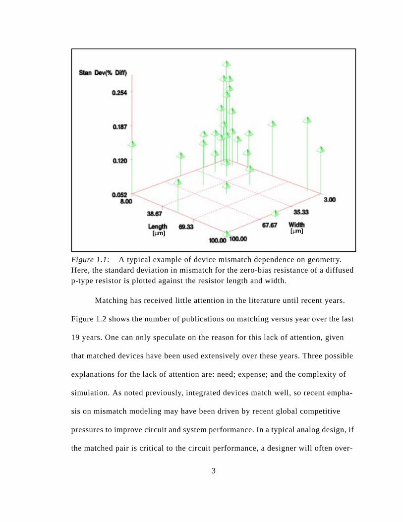
plotted against the device geometry as in Figure 1.1, the dependence of devi
mismatch on geometry is apparent. Here, it can be seen that the mismatch d
sion improves somewhat asymptotically as the length and/or width of the dev
increases. This is one component of mismatch modeling.
2
sed
.
last
n
ssible
of
ha-
n, if
er-
Figure 1.1: A typical example of device mismatch dependence on geometry.Here, the standard deviation in mismatch for the zero-bias resistance of a diffup-type resistor is plotted against the resistor length and width.
Matching has received little attention in the literature until recent years
Figure 1.2 shows the number of publications on matching versus year over the
19 years. One can only speculate on the reason for this lack of attention, give
that matched devices have been used extensively over these years. Three po
explanations for the lack of attention are: need; expense; and the complexity
simulation. As noted previously, integrated devices match well, so recent emp
sis on mismatch modeling may have been driven by recent global competitive
pressures to improve circuit and system performance. In a typical analog desig
the matched pair is critical to the circuit performance, a designer will often ov
[µm][µm]
3

to
since
ame-
onfi-
s,
it
size the matched devices and use layout techniques such as cross-coupling
obtain the best matching possible. However, these techniques are expensive
they consume a lot of space on the layout.
Second, mismatch is a statistical measure, and unlike other device par
ters, many dice must be measured in order to obtain a value with reasonable c
dence. Mismatch measurements also require high resolution from the
measurement equipment. This implies more complex measurement algorithm
and many more samples across lots, wafers, and dice.
Figure 1.2: A bar chart showing the number of publications on integrated circudevice mismatch over time.
** 1999 is an incomplete year
4

li-
ula-
if
cir-
e-
s
as
ica-
itic
s.
r,
s of
gap
act
The third speculation refers to statistical modeling. Although many pub
cations have given extensive coverage to this topic, modern-day statistical sim
tion tools are either too time consuming, too inaccurate, or both. Thus, even
accurate mismatch models were developed, their use would be limited to hand
cuit calculations.
Most of the literature on matching has been dedicated to MOSFETs, pr
sumably due to the proliferation of CMOS processes in the industry. There ha
been little published on bipolar transistor matching. Although CMOS analog h
some advantages, there is still a need for bipolar analog for such circuit appl
tions as band-gap voltage references. Additionally, there is at least one paras
bipolar in any non-SOI CMOS process. Generally speaking, BJTs have better
matching performance than MOSFETs.
Like the bipolars, little has been published on resistor matching.
1.3 Outline for this thesis
The scope of this paper is limited to homojunction silicon devices,
although the concepts are directly transferable to other materials. This paper
begins by exploring the impact of mismatched devices on typical circuit block
At least one example is given for each of a bipolar transistor, a MOS transisto
and a resistor. Two new mismatch circuit analyses are given. The contribution
bipolar transistor mismatch and resistor mismatch to the variability of a band
voltage reference are determined and the optimum ratio for minimizing the imp
5

e
og
ral
ta-
pri-
om
of
reti-
en-
sis-
fac-
ting
n for
r
atch
S
of mismatch on the voltage reference variability is demonstrated. Likewise, th
contributions for several matched resistors in a voltage scaling digital to anal
converter is derived.
Much of matching theory is common to transistors and resistors. A gene
discussion on matching theory is provided first, followed by a small review of s
tistical modeling and the role of mismatch in statistical modeling. Some of the
mary early papers are reviewed with an analysis of the geometric sampling fr
these papers. An improved experimental design is given for characterization
mismatch over the geometry space.
Topics specific to resistor mismatch are discussed in Chapter 4. A theo
cally based model is derived which conforms to the previously derived experim
tal design. This model was applied to five diffused resistors from a 0.8µm power
BiCMOS technology. It is demonstrated heuristically that both the diffused re
tor junction depth and the ion implantation dose concentration are significant
tors in determining the sheet resistance mismatch variability. Several new plot
schemes for depicting mismatch over geometry space are presented. A solutio
the lowest mismatch for a fixed resistor area is derived which can be useful fo
plotting.
Topics specific to MOSFETs are discussed in Chapter 5. Previous mis-
match modeling approaches are reviewed. A new model and method for mism
characterization are presented. The nMOS and pMOS devices from a BiCMO
6

alysis
f the
is
he
min-
5,
ns
atch
mis-
on-
process and a deep submicron CMOS process are presented. A combined an
of the nMOS and pMOS devices was used to extract a more robust estimator o
gate oxide thickness mismatch variability. A comparison against prior models
given to demonstrate the features of the new model. Finally, a discussion of t
mismatch model parameter sensitivities leads to a experimental design with a
imum number of treatment combinations.
Topics specific to BJTs are discussed in Chapter 6. Similar to Chapter
prior work in modeling the BJT mismatch is reviewed and the new model and
characterization approach are given. Plots across geometry and bias conditio
demonstrate the accuracy of the model. An additional experiment shows mism
data for multiple collector biases and temperatures in comparison to the new
match model. A new method for rapid evaluation of the physical cause of BJT
mismatch is presented.
Finally, the main features and discoveries of this work are given in the c
clusion.
7

al
mple
wn
BJT,
Chapter 2 The Significance of Matching - Examples
In order to demonstrate the importance of matching in analog and digit
design, several real world examples are given. Throughout these examples, a
use is made of the propagation of variance (POV) equation,
(2.1)
in which the variance of an independent parameter, is related to the variance of
the dependent parameter via a local linearization of the dependency.
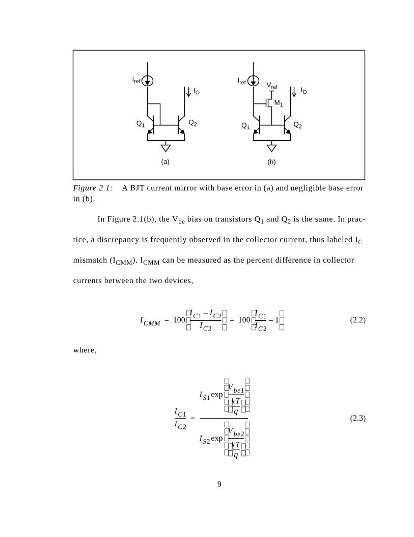
2.1 Example 1 - A BJT current mirror
Perhaps the simplest example of matching is the current mirror. As sho
in Figure 2.1 (a), a reference current is passed through the diode connected
Q1. The Vbe bias on Q1 is duplicated on the base/emitter of Q2, thereby generating
a “mirror” current of IO which is nearly equal to Iref. The current IO is not an exact
mirror of Iref due to the base current supply coming from Iref. The mirror current,
IO is in fact a mirror of the quantity, (Iref - Ib1 - Ib2). Techniques such as the one
shown in Figure 2.1 (b) can be used to minimize the impact of this error.
σy2
x∂∂y
2
σx2
=
σx2
σy2
8
or
d I
r
Figure 2.1: A BJT current mirror with base error in (a) and negligible base errin (b).
In Figure 2.1(b), the Vbe bias on transistors Q1 and Q2 is the same. In prac-
tice, a discrepancy is frequently observed in the collector current, thus labeleC
mismatch (ICMM). ICMM can be measured as the percent difference in collecto
currents between the two devices,
(2.2)
where,
(2.3)
Vref
Q1 Q2 Q1 Q2
M1
IrefIref
(a) (b)
IO IO
I CMM 100I C1 I C2–
I C2-----------------------
100I C1
I C2-------- 1–
= =
I C1
I C2--------
I S1
Vbe1
kTq
------ ------------
exp
I S2
Vbe2
kTq
------ ------------
exp
------------------------------------=
9

tion
e
by
des
ld
not
e
where Vbe is the base / emitter voltage and Is is the saturation current. Vbe1= Vbe2
so, assuming only diffusion current, neglecting the BJT emitter-base backinjec
current, and recombination currents,
(2.4)
where A1 and A2 are the emitter areas, De1 and De2 are the electron diffusion
constants in the base, NA1(x) and NA2(x) are the base dopant concentration
profiles, and WB1 and WB2 are the base widths for Q1 and Q2 respectively. From
Eq. (2.4) it is evident that ICMM results from mismatches in the emitter area, th
base dopant concentration/profile, and/or the base width.
It should be noted that the collector currents in Eq. (2.4) can be ratioed
selecting the appropriate ratio in emitter areas.1 Thus, the concept of device
matching is not limited to identically drawn devices. The base and emitter no
of Q1 in Figure 2.1(a) can also be used to bias multiple BJTs which in turn wou
provide multiple current sources from a single reference. So, matching is also
limited to just two devices.
1. Aside from the noted base current offset, the ratio of emitter areas is not exactly preserved in thcollector current ratios. This results from the perimeter and corner components of the emit-ter/base junction injection current which do not scale with the emitter area.
I C1
I C2--------
I S1
I S2-------
A1 De1 x( )NA2
x( ) xδWB2
∫
A2 De2 x( )NA1
x( ) xδWB1
∫------------------------------------------------------------= =
10
ro-
ub-
as
ua-
ligi-
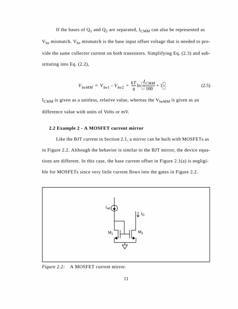
If the bases of Q1 and Q2 are separated, ICMM can also be represented as
Vbe mismatch. Vbe mismatch is the base input offset voltage that is needed to p
vide the same collector current on both transistors. Simplifying Eq. (2.3) and s
stituting into Eq. (2.2),
(2.5)
ICMM is given as a unitless, relative value, whereas the VbeMM is given as an
difference value with units of Volts or mV.
2.2 Example 2 - A MOSFET current mirror
Like the BJT current in Section 2.1, a mirror can be built with MOSFETs
in Figure 2.2. Although the behavior is similar to the BJT mirror, the device eq
tions are different. In this case, the base current offset in Figure 2.1(a) is neg
ble for MOSFETs since very little current flows into the gates in Figure 2.2.
Figure 2.2: A MOSFET current mirror.
VbeMM Vbe1 Vbe2–kTq
------I CMM
100--------------- 1+
ln= =
M1 M2
Iref
IO
11
rent
nd
xide
ant
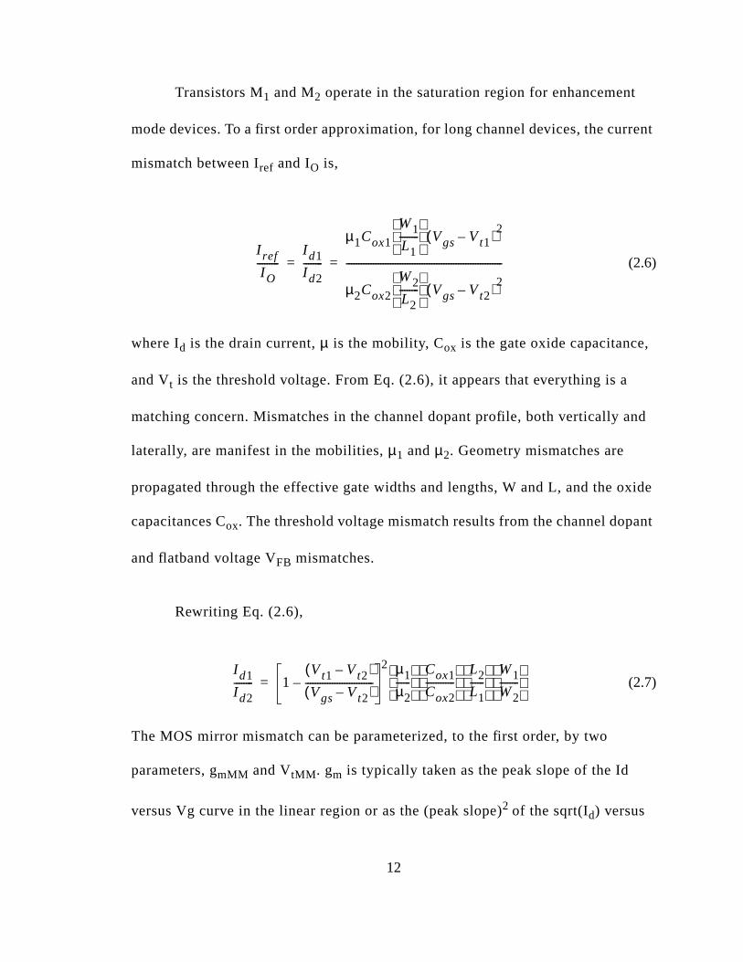
Transistors M1 and M2 operate in the saturation region for enhancement
mode devices. To a first order approximation, for long channel devices, the cur
mismatch between Iref and IO is,
(2.6)
where Id is the drain current,µ is the mobility, Cox is the gate oxide capacitance,
and Vt is the threshold voltage. From Eq. (2.6), it appears that everything is a
matching concern. Mismatches in the channel dopant profile, both vertically a
laterally, are manifest in the mobilities,µ1 andµ2. Geometry mismatches are
propagated through the effective gate widths and lengths, W and L, and the o
capacitances Cox. The threshold voltage mismatch results from the channel dop
and flatband voltage VFB mismatches.
Rewriting Eq. (2.6),
(2.7)
The MOS mirror mismatch can be parameterized, to the first order, by two
parameters, gmMM and VtMM. gm is typically taken as the peak slope of the Id
versus Vg curve in the linear region or as the (peak slope)2 of the sqrt(Id) versus
I ref
I O---------
I d1
I d2--------
µ1Cox1
W1
L1--------
Vgs Vt1–( )2
µ2Cox2
W2
L2--------
Vgs Vt2–( )2
----------------------------------------------------------------= =
I d1
I d2-------- 1
Vt1 Vt2–( )Vgs Vt2–( )
----------------------------–2 µ1
µ2------
Cox1
Cox2------------
L2
L1------
W1
W2--------
=
12

of
s,
Vg curve in the saturation region. It encompasses the mobility, Cox, and geometry
parameters from the Id relationship in Eq. (2.6). VtMM is the difference in
threshold voltage between the two devices. Eq. (2.7) can be rewritten,
(2.8)
Note that the “2” subscript has been removed from Vt in the denominator of
Eq. (2.8), since the mismatch in Vt is negligible in comparison to the gate over-
drive, (Vgs-Vt).
An interesting result from Eq. (2.7) and Eq. (2.8) is the bias dependence
IdMM on the gate voltage.1 VtMM only plays an important roll in the IdMM when
the quantity (Vgs-Vt) is small. Otherwise, the IdMM is dominated by the gmMM.
It is worthwhile to examine Eq. (2.7) in further detail. Since only the ratio
and not the absolute values, of Id1, Id2, µ1, µ2, Cox1, Cox2, L1, L2, W1, and W2 are
relevant, Eq. (2.7) is rewritten to,
(2.9)
1. It would appear from Section 2.1 and 2.2 that the MOS Id mismatch is bias dependent and theBJT Ic mismatch is bias independent. Although the first order analysis of BJT Ic mismatch didnot show the bias dependence, a more detailed analysis in Chapter 6 will show this.
I d1
I d2-------- 1
VtMM
Vgs Vt–( )-------------------------–
2 gm1
gm2---------
=
r Id 1VtMM
Vgs Vt–( )-------------------------–
2
rµ( ) rC( ) 1r L-----
rW( )=
13
d as a
he
e
spite
l
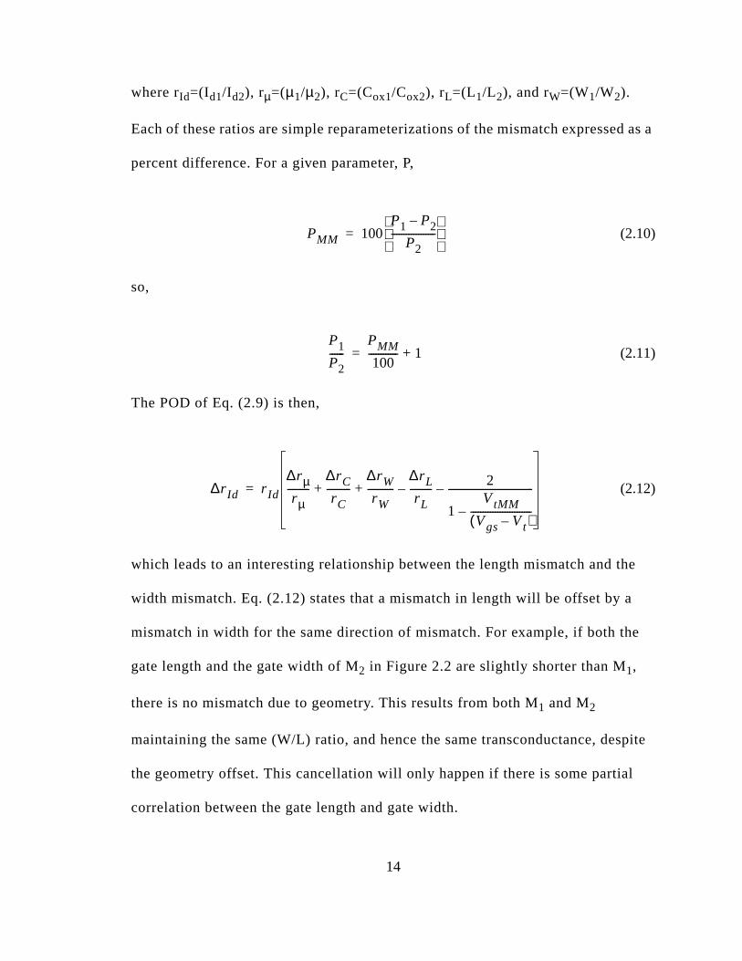
where rId=(Id1/Id2), rµ=(µ1/µ2), rC=(Cox1/Cox2), rL=(L1/L2), and rW=(W1/W2).
Each of these ratios are simple reparameterizations of the mismatch expresse
percent difference. For a given parameter, P,
(2.10)
so,
(2.11)
The POD of Eq. (2.9) is then,
(2.12)
which leads to an interesting relationship between the length mismatch and t
width mismatch. Eq. (2.12) states that a mismatch in length will be offset by a
mismatch in width for the same direction of mismatch. For example, if both th
gate length and the gate width of M2 in Figure 2.2 are slightly shorter than M1,
there is no mismatch due to geometry. This results from both M1 and M2
maintaining the same (W/L) ratio, and hence the same transconductance, de
the geometry offset. This cancellation will only happen if there is some partia
correlation between the gate length and gate width.
PMM 100P1 P2–
P2------------------
=
P1
P2------
PMM
100------------ 1+=
∆r Id r Id
∆rµrµ
---------∆rC
rC----------
∆rW
rW-----------
∆r L
rL---------– 2
1VtMM
Vgs Vt–( )-------------------------–
-----------------------------------–+ +=
14
ess
ese
nse-
n
s
a
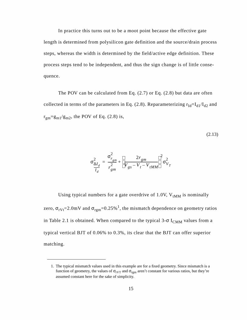
In practice this turns out to be a moot point because the effective gate
length is determined from polysilicon gate definition and the source/drain proc
steps, whereas the width is determined by the field/active edge definition. Th
process steps tend to be independent, and thus the sign change is of little co
quence.
The POV can be calculated from Eq. (2.7) or Eq. (2.8) but data are ofte
collected in terms of the parameters in Eq. (2.8). Reparameterizing rId=Id1/Id2 and
rgm=gm1/gm2, the POV of Eq. (2.8) is,
(2.13)
Using typical numbers for a gate overdrive of 1.0V, VtMM is nominally
zero,σrVt=2.0mV andσrgm=0.25%1, the mismatch dependence on geometry ratio
in Table 2.1 is obtained. When compared to the typical 3-σ ICMM values from a
typical vertical BJT of 0.06% to 0.3%, its clear that the BJT can offer superior
matching.
1. The typical mismatch values used in this example are for a fixed geometry. Since mismatch isfunction of geometry, the values ofσrVT andσrgm aren’t constant for various ratios, but they’reassumed constant here for the sake of simplicity.
σ∆I d
I d---------
2σr gm
2
rgm2
-----------2rgm
Vgs Vt– VtMM–-----------------------------------------
2
σVT
2+=
15
f.0
c-
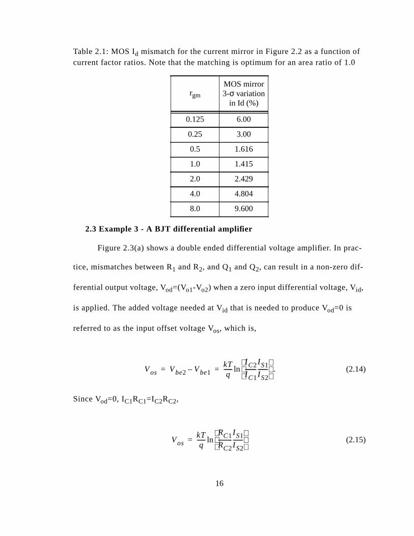
Table 2.1: MOS Id mismatch for the current mirror in Figure 2.2 as a function ocurrent factor ratios. Note that the matching is optimum for an area ratio of 1
2.3 Example 3 - A BJT differential amplifier
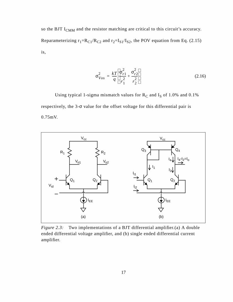
Figure 2.3(a) shows a double ended differential voltage amplifier. In pra
tice, mismatches between R1 and R2, and Q1 and Q2, can result in a non-zero dif-
ferential output voltage, Vod=(Vo1-Vo2) when a zero input differential voltage, Vid,
is applied. The added voltage needed at Vid that is needed to produce Vod=0 is
referred to as the input offset voltage Vos, which is,
. (2.14)
Since Vod=0, IC1RC1=IC2RC2,
(2.15)
rgm
MOS mirror3-σ variation
in Id (%)
0.125 6.00
0.25 3.00
0.5 1.616
1.0 1.415
2.0 2.429
4.0 4.804
8.0 9.600
Vos Vbe2 Vbe1–kTq
------I C2
I C1--------
I S1
I S2-------
ln= =
VoskTq
------RC1
RC2----------
I S1
I S2-------
ln=
16
.
so the BJT ICMM and the resistor matching are critical to this circuit’s accuracyReparameterizing r1=RC1/RC2 and r2=IS1/IS2, the POV equation from Eq. (2.15)
is,
(2.16)
Using typical 1-sigma mismatch values for RC and IS of 1.0% and 0.1%
respectively, the 3-σ value for the offset voltage for this differential pair is
0.75mV.
Figure 2.3: Two implementations of a BJT differential amplifier.(a) A doubleended differential voltage amplifier, and (b) single ended differential currentamplifier.
σVos2 kT
q------
σr12
r12
--------σr2
2
r22
--------+
=
Q2
I1
Q1
Q3 Q4
I4
I2
I4-I2=Io
IEE
Q2Q1
IEE
R1 R2
Vo1 Vo2
Vcc
Vid
Vcc
(a) (b)
Ii1
Ii2
17

n
ut
In Figure 2.3(b) a single ended differential current amplifier is given,
where the output current, IO is based upon the differential current input betwee
I i1 and Ii2. Ignoring the base current offset in the PNP current mirror, the outp
current is,
(2.17)
where through are the collector currents for Q1 through Q4, and is
the mismatch in Q3 and Q4. To produce a zero output current,
(2.18)
The offset current, IOS, that is needed at the differential input is
(2.19)
This introduces a new matching parameter,βMM, which is the mismatch in the
BJT gain,β. Setting rIb=Ib1/Ib2, rβ=β1/β2, and rIc=IC3/IC4, the POV of Eq. (2.19)
is,
(2.20)
I O I 4 I 2– I C4 I C2–I C4
I C3--------
I C1 I C2–= = =
I C1 I C4
I C4
I C3--------
I C2
I C1--------
I C4
I C3--------
=
I b1
I b2-------
β2
β1------
I C3
I C4--------
=
σr Ib
2
r Ib2
---------σrβ
2
rβ2
--------σr Ic
2
r Ic2
---------+=
18

-
h
sis-
t-
S
-
that
ave
have
ing
d in
Using a typical Beta mismatch of 0.25% and ICMM of 0.1%, a 3-sigma variation in
the offset current is 0.27%.
2.4 Example 4 - A voltage scaling DAC
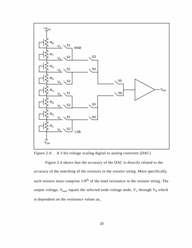
Figure 2.4 shows a simple 3 bit digital to analog converter (DAC) imple
mented with matched resistors from [4]. A constant current flows from the hig
rail to the low rail, providing a constant I-R voltage drop across each of the re
tors. Switches S1 and S2 are controlled by the first digital input bit, S3 and S4 are
controlled by the second bit, and S5 and S6 are controlled by the third bit. In
implementation, S1 through S6 are substituted with MOS pass transistors. The ou
put, Vout is buffered to prevent any appreciable current flow through switches 1-
S6 which would divert current flow from the resistor string and thereby compro
mise the DAC accuracy.
The resistors in Figure 2.4 are given different subscripts to emphasize
these resistors have different values of resistance despite the fact that they h
been designed/laid-out to have the same resistances. These diffused resistors
a well bias dependence which is shown by the third terminal. To prevent a skew
of the resistances due the backgate voltage coefficient, each resistor is place
its own tub with a local connection to the tub.
19
lly,
e
Figure 2.4: A 3 bit voltage scaling digital to analog converter (DAC)
Figure 2.4 shows that the accuracy of the DAC is directly related to the
accuracy of the matching of the resistors in the resistor string. More specifica
each resistor must comprise 1/8th of the total resistance in the resistor string. Th
output voltage, Vout, equals the selected node voltage node, V1 through V8 which
is dependent on the resistance values as,
S1
S2
S1
S2
S1
S2
S1
S2
S5
S6
S3
S4
S3
S4
R8
+Vref
-Vref
R7
R6
R5
R3
R2
R1
R4 Vout
V7
V6
V5
V4
V2
V1
V0
V3
MSB
LSB
20

(2.21)
Assuming that the eight resistors are iid(0,σR2)1 and there is no variability
in the voltage supply rails,
. (2.22)
The nodal voltage sensitivity is,
(2.23)
Substitution of Eq. (2.23) into Eq. (2.22) yields the approximation,
(2.24)
or,
(2.25)
1. iid(0,σR2) means independently and identically distributed with mean=0 and variance=σR
2.
Vout Vn
Rii 1=
n
∑
Rii 1=
8
∑---------------- Vref Vref–( )–( ) Vref–= =
σVn2
Ri∂∂Vn
2
i 1=
n
∑ σR2
=
Ri∂∂Vn 1
Rjj 1=
8
∑----------------- 1
Rjj 1=
n
∑
Rjj 1=
8
∑-----------------– 2Vref( )=
σVn2
4Vref2
n1
RT2
-------
1 n8---–
2σR
2≈
σVn 2Vrefn
8------- 1 n
8---–
σR=
21

re
o
r
olt-
stor
um-
n-
where the tilde (~) above theσ denotes that this is a relative, unitless value and RT
is the total resistance in the resistor string. In the general case where there a
T=2m resistors from a m-bit DAC,
(2.26)
Eq. (2.25) and Eq. (2.26) imply that the variability of the output voltage due t
resistor matching is dependent on the bit selection.
A typical diffused resistor has a mismatch of about 1.0 percent1. The corre-
sponding variability in the output voltage due to resistor mismatch is given in
Table 2.2.
It is interesting to note that the Vout variability, due to matching, peaks nea
the middle nodes. The variability in Vout=V0 is zero because this node is hard-
wired to the negative rail, hence the resistor variability does not affect output v
age in this case. At the other end of the resistor string (near the MSB), the resi
variability is included in both the numerator summation and the denominator s
mation of Eq. (2.21), producing a cancelling effect.
1. Resistor mismatch values range from 0.05% to 5.0% depending on the size, spacing, and orietation of the resistors. It should be noted in this example that the goal is to simultaneously matcheight resistors. It is impossible to place each of the eight resistors at minimum separation dis-tance from the other seven resistors that it is respectively matching. Thus process gradientsbecome a concern and the matching could be further degraded.
σVn 2Vrefn
T------- 1 n
T---–
σR=
22

.4.
e
r the
ques-
e
nch
ith
a
ch-
Table 2.2: Table of variabilities due to resistor matching in the DAC of Figure 2A resistor mismatch of 1.0% was assumed for this example
2.5 Example 5 - A band gap voltage reference.
Although the significance of BJT matching has been demonstrated in th
previous examples, in all of these examples, MOSFETs can be substituted fo
BJTs. Hence a designer who designs in a CMOS only process might ask the
tion, “Why should I care about bipolar transistor matching?” The answer is th
band gap voltage reference.
Every CMOS process that does not contain an SOI substrate and a tre
isolation, is guaranteed to contain a parasitic BJT. Even if the process is SOI w
a trench isolation, the MOSFETs can be implemented as lateral BJTs through
change in bias. Although this often leads to aggravating problems such as lat
Bit Vout = σVn/Vref (%)σVn (mV)assumingVref=5v
LSB V0 0.0 0.0
V1 0.219 10.95
V2 0.266 13.3
V3 0.270 13.5
V4 0.250 12.5
V5 0.210 10.5
V6 0.154 7.7
MSB V7 0.0826 4.13
23

ltage
era-
a
ch a
up, the parasitic BJT can be used to the designer’s advantage as a band gap vo
reference.
The band gap voltage reference takes advantage of the opposing temp
ture coefficients of a BJT base/emitter bias and a diffused resistor to produce
voltage reference that is, to the first order, independent of temperature [5]. Su
circuit is given in Figure 2.5.
The supply voltage, VO, in Figure 2.5 is,
(2.27)
where,
(2.28)
and the ratio of currents I1/I2 is,
(2.29)
The current, I2, is nearly the same through resistors R2 and R3 since the
subtraction of the base current for Q3 is roughly replaced by the Q2 base current.
VO Vbe3 I 2R2+=
R3I 2kTq
------I 1
I 2-----
I S2
I S1-------
ln=
I 1
I 2-----
VO Vbe1–
R1--------------------------
VO Vbe3–
R2--------------------------
-------------------------------
R2
R1------≅=
24
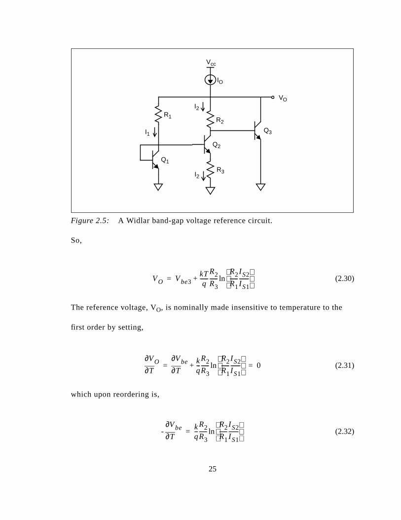
Figure 2.5: A Widlar band-gap voltage reference circuit.
So,
(2.30)
The reference voltage, VO, is nominally made insensitive to temperature to the
first order by setting,
(2.31)
which upon reordering is,
- (2.32)
IO
R1
VO
Vcc
R2
R3
Q1
Q2
Q3I1
I2
I2
VO Vbe3kTq
------R2
R3------
R2
R1------
I S2
I S1-------
ln+=
T∂∂VO
T∂∂Vbe k
q---
R2
R3------
R2
R1------
I S2
I S1-------
ln+ 0= =
T∂∂Vbe k
q---
R2
R3------
R2
R1------
I S2
I S1-------
ln=
25

he
are
it
is-
32)
This
ini-
ch
tor
df.
where is a constant, and R2, R3, R1, Q1 and Q2 are used to tune the opposing
temperature coefficients so that Eq. (2.32) is satisfied. It is evident from Eq.
(2.32), that the matching of R2 to R3, R1 to R2, and Q1 to Q2 are critical to
delivering a precision voltage reference. The absolute behavior of R1, R2, R3, Q1,
and Q2 are irrelevant in this analysis. The traditional solution for the values of t
resistors and transistors in Eq. (2.32) is an underdetermined problem. There
three degrees of freedom (df) for the solution but there is only one objective
criteria.
In a real world implementation of this circuit or any other bandgap circu
in silicon, there is always variability in the matching of the resistors and trans
tors. This implies that with some parts, the left- and right-hand sides of Eq. (2.
will not always be equal. However, the variance of the right-hand side of Eq.
(2.32) that is due to mismatch variations is also dependent on the three ratios.
provides an opportunity to choose the three ratios that satisfy Eq. (2.32) and m
mize the variance of Eq. (2.32).
If the mismatch variability is assumed to be constant over all values of ea
ratio, the three mismatch ratios in Eq. (2.32) fold down into two df’s. The resis
ratio and the BJT current mismatch inside of the natural log comprise the same
T∂∂Vbe
26

int.
In addition, only the ratios and not the absolute values are of interest at this poThus is combined into a single value A2. A1 is the ratio, .
dVbe/dT is assumed constant over process variations which means,
(2.33)
where is the offset in slope of VO with respect to temperature and S is the
nominal slope.
The propagation of a deviation (POD) from the device mismatches to
is,
(2.34)
where∆ is change due to variations in mismatch of process and geometry
parameters. The propagation of variance (POV) from the variance of the ratio
mismatches to the variance of the temperature sensitivity is,
(2.35)
R2
R1------
I S2
I S1-------
R2
R3------
∆T∂
∂VO
A1 A2mismatch,
∆T∂
∂Vbe
A1 A2mismatch,
∆ ∆S= =
∆S
∆S
∆SA1∂
∂S ∆A1 A2∂∂S ∆A2+
kq--- A2( )∆A1ln
kq---
A1
A2------∆A2+= =
σS2 k
q--- A2( )ln
2σA1
2 kq---
A1
A2------
2
σA2
2 k2
q2
-----A1 A2( )ln
A2------------------------σA1
σA2r12+ +=
27

e
1%
the
whereσ is the mismatch variance for ratios A1 and A2 and r12 is the correlation
coefficient between A1 and A2. Eq. (2.35) is the second condition that should b
optimized in conjunction with the solution of Eq. (2.32). The first term in Eq.
(2.35) is the POV from the R2 -R3 resistor mismatch, and the second term is the
POV from the R1 - R2 mismatch and the Q1 - Q2 Ic mismatch. The third term is the
combined sensitivity due to all three mismatch contributors. The third term is
required because of the potential partial correlation between the A1 and A2 ratios
since R2 appears in both ratios.
A typical value of dVbe/dT at room temperature is -2.0 mV/C. In order to
satisfy Eq. (2.31), R2/R3*ln(I 1/I2)=23.1. If typical 1-sigma values for the zero-
bias resistance mismatch and BJT collector current mismatch of 1.0% and 0.
are assumed, the reference voltage mismatches in Table 2.3 are obtained.
Table 2.3: Offset values in the reference voltage sensitivity to temperature in bandgap circuit in Figure 2.5. A typical 1-sigma RMM of 1.0% in R2 and R3 and 1-sigma ICMM of 0.1% in Q1 and Q2 was assumed.
A1 A2dVO/dT (µV/C)(3-sigma value)
33.33 2.0 43.2
14.353 5.0 8.52
10.03 10.0 6.50
7.711 20.0 7.82
5.905 50.0 10.14
5.016 100 11.9
28

e
r
.
From Table 2.3, it is apparent that there is a trade-off in the between th
two ratios. There is an optimum selection of ratios somewhere around 10.0 fo
both A1 and A2 in which the susceptibility to mismatch variations is minimized
Eq. (2.32) and Eq. (2.35) can be combined by rewriting Eq. (2.32) as,
(2.36)
where the constant, k1, is,
(2.37)
Substitution of Eq. (2.36) into Eq. (2.35) yields,
(2.38)
Eq. (2.38) can be minimized by setting,
(2.39)
A2
k1
A1------
exp=
k1 T∂∂Vbe q
k---
–=
σS2 k
q---
k1
A1------
2
σA1
2 kq---A1
k1
A1------–
exp 2
σA2
2 k2
q2
-----k1
k1
A1------–
exp σA1σA2
r12+ +=
A1∂∂ σS
2( ) 2A1k
2
q2
----- 1K1
A1-------+
2k1
A1--------–
σA2
2exp 2
k2
q2
-----k1
2
A13
------σA1
2–
k2
q2
-----k1
2
A12
------k1
A1------–
exp σA1σA2
r12+ 0
=
=
29

.3.
which can be iteratively solved for A1 since it is transcendental. If we use the
values from the previous example, we find that the optimum value for A1 and A2
are as listed in Table 2.4 which coincides with the apparent optimum in Table 2
Table 2.4: Optimum ratios for A1 and A2 for the Widlar bandgap voltage referencein Figure 2.5 for three different correlation coefficients.
r12 A1 A2dVO/dT (µV/C)(3-sigma value)
0 10.675 8.76 6.45
0.5 10.25 9.575 7.07
1.0 9.85 10.51 7.60
30
et
in
atic
ts.
and
com-
m
nd
Chapter 3 General Mismatch Principles
3.1 Sources of mismatch
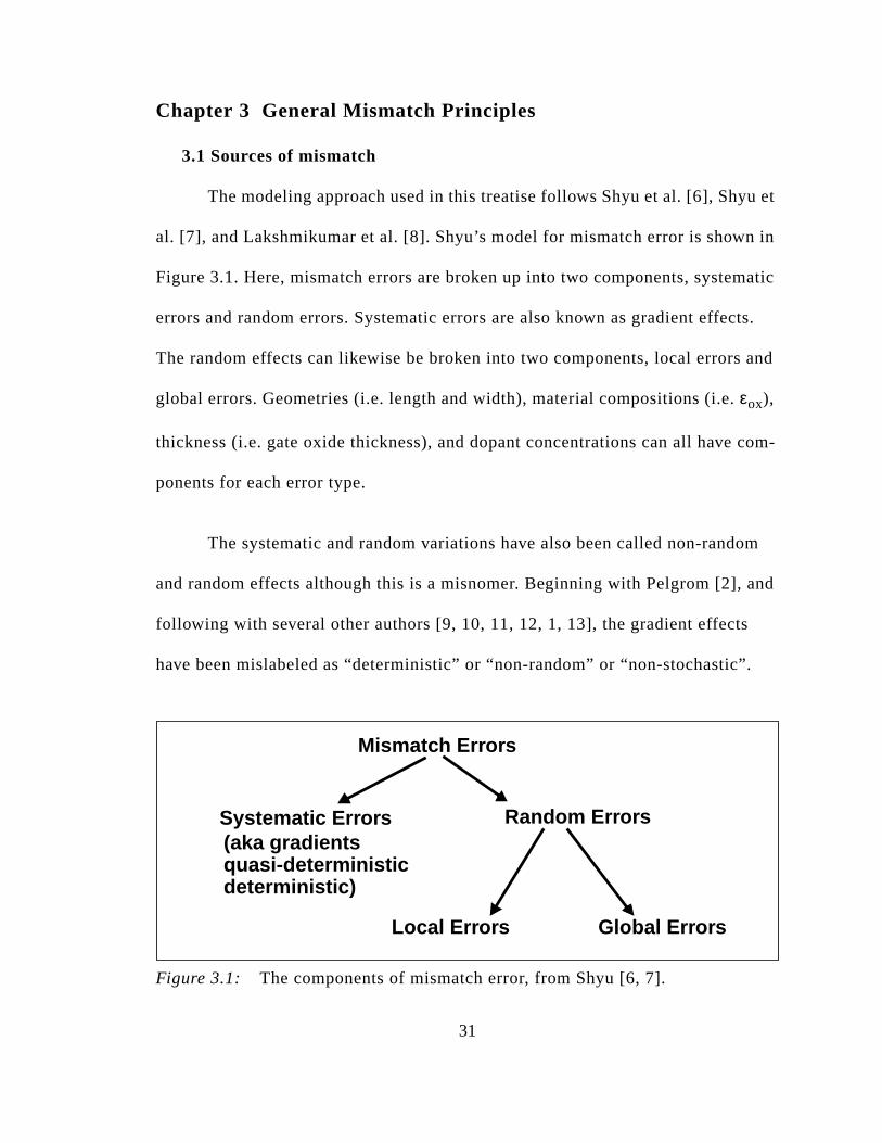
The modeling approach used in this treatise follows Shyu et al. [6], Shyu
al. [7], and Lakshmikumar et al. [8]. Shyu’s model for mismatch error is shown
Figure 3.1. Here, mismatch errors are broken up into two components, system
errors and random errors. Systematic errors are also known as gradient effec
The random effects can likewise be broken into two components, local errors
global errors. Geometries (i.e. length and width), material compositions (i.e.εox),
thickness (i.e. gate oxide thickness), and dopant concentrations can all have
ponents for each error type.
The systematic and random variations have also been called non-rando
and random effects although this is a misnomer. Beginning with Pelgrom [2], a
following with several other authors [9, 10, 11, 12, 1, 13], the gradient effects
have been mislabeled as “deterministic” or “non-random” or “non-stochastic”.
Figure 3.1: The components of mismatch error, from Shyu [6, 7].
Mismatch Errors
Systematic Errors Random Errors
Local Errors Global Errors
(aka gradientsquasi-deterministicdeterministic)
31
s-
:
of
od-
t.
a-
led
rge
and
,
to
ching
atch
by
-
ched
e lay-
Webster’s Ninth New Collegiate Dictionary gives the definition of stocha
tic as “Random: involving a random variable” or “involving chance or probability
probabilistic.” Likewise this same dictionary defines determinacy as “the state
being definitely and unequivocally characterized”. Since all gradients are a pr
uct of processing conditions, they will always contain a stochastic componen
The slope or offset will be a little bit different for each wafer and lot. A given gr
dient can be, at best, only partially determined or “quasi-deterministic” as labe
by Pavasovic [14].
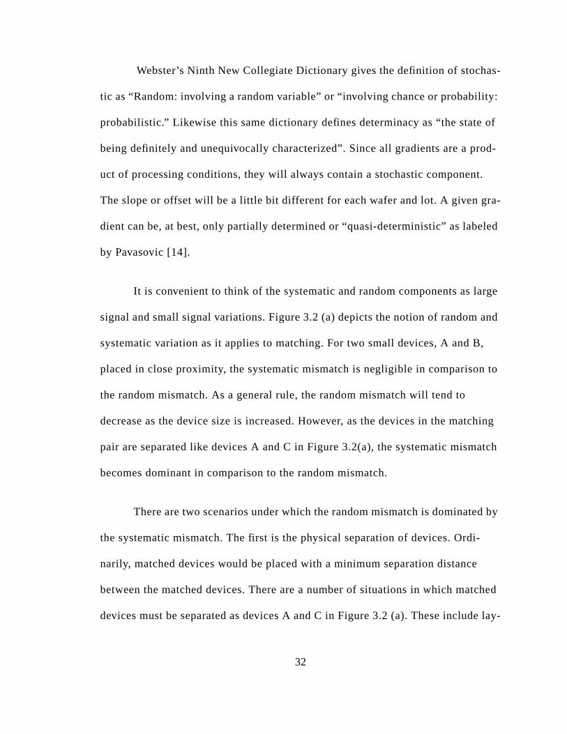
It is convenient to think of the systematic and random components as la
signal and small signal variations. Figure 3.2 (a) depicts the notion of random
systematic variation as it applies to matching. For two small devices, A and B
placed in close proximity, the systematic mismatch is negligible in comparison
the random mismatch. As a general rule, the random mismatch will tend to
decrease as the device size is increased. However, as the devices in the mat
pair are separated like devices A and C in Figure 3.2(a), the systematic mism
becomes dominant in comparison to the random mismatch.
There are two scenarios under which the random mismatch is dominated
the systematic mismatch. The first is the physical separation of devices. Ordi
narily, matched devices would be placed with a minimum separation distance
between the matched devices. There are a number of situations in which mat
devices must be separated as devices A and C in Figure 3.2 (a). These includ
32
n a
ay
(a),
the
s
ion
out constraints in which a non-critical pair may be separated in order to obtai
more compact layout. A second scenario is multiple matched devices which m
be encountered with current sources or with the resistors as in Section 2.4.
The second scenario has to do with the device geometry. In Figure 3.2
two small devices, A and B, are placed at a minimum separation distance. As
device width is increased as in Figure 3.2 (b), the center-to-center spacing ha
increased. Thus, despite that the devices are still placed at minimum separat
distance, this matching pair is dominated by systematic errors.
Figure 3.2: Graphical depiction of random and systematic variations.
Dev
ice
A
Dev
ice
BD
evic
e C
Dev
ice
A
Dev
ice
B local MM variation
global MM variation
(a)
(b)Lateral position on the wafer
Loca
l dev
ice
perfo
rman
ceLo
cal d
evic
epe
rform
ance
Lateral position on the wafer
33

In
gh
ccur
aria-
n,
mity
3.1.1 Random errors
The distinction between local and global errors is shown in Figure 3.3.
(a), possible sources for local mismatch are polysilicon or metal grain edge
boundaries, local etch variation, or local implant or diffusion variations. Althou
only the edge variations are shown in Figure 3.3, local mismatches can also o
through-out the area of the device. Such sources for local mismatch include v
tions in gate oxide thickness or permittivity and dopant variations.
Potential sources for global mismatch variation include line edge variatio
dopant variations, stepper lens aberrations, loading effects, and optical proxi
shifts.
Figure 3.3: A comparison of local and global mismatch errors
(a) Local Mismatch (b) Global Mismatch
∆L
l(x)
xyL
L
W
34

tem-
vice
hoto-
. It is
cen-
re
an
adial,
a
s-
3.1.2 Systematic errors
Large signal variation results from gradients in processing, stress, and
perature. Thus, the process, design, and package must be considered for de
matching.
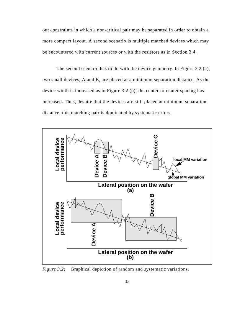
Wafer processing gradients can be placed into two categories, radially
based gradients and monotonic gradients. Examples of radial gradients are p
resist coat, development, hot-plate bakes, plasma etch, and some depositions
important to note that any of the “spin-coat” processes will have a near-exact
ter with concentric circles of contour as shown in Figure 3.4(a). Other single
wafer processing steps can produce a radially based gradient such as in Figu
3.4(b) or (c), where the center of the radial pattern is substantially different th
the wafer center and the contours are less regular. Process gradients may be r
linear or otherwise spatially dependent, but given the proximity of devices in
matching pair, it is reasonable to consider all gradients to be linear1.
1. The linearity assumption is sufficient for matched devices in analog design. This assumption inot appropriate for devices with large separations such as clock skew matching in digital applications.
35
rrypro-
are
ed
se a
per-
cts
par-
ice
nts
yond
Figure 3.4: Three depictions of radially based wafer gradients. In (a), a wafefrom a “spin-coat” process will have a near-exact center on the wafer with veregular concentric circles of contour. Other single wafer processing steps canduce a radially based gradient such as in (b) or in (c), where the center of theradial pattern is substantially different than the wafer center and the contour less regular.
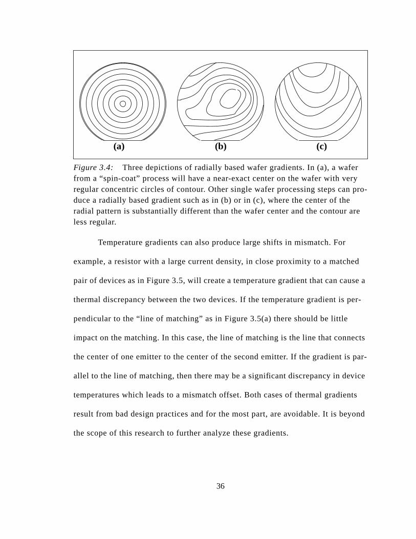
Temperature gradients can also produce large shifts in mismatch. For
example, a resistor with a large current density, in close proximity to a match
pair of devices as in Figure 3.5, will create a temperature gradient that can cau
thermal discrepancy between the two devices. If the temperature gradient is
pendicular to the “line of matching” as in Figure 3.5(a) there should be little
impact on the matching. In this case, the line of matching is the line that conne
the center of one emitter to the center of the second emitter. If the gradient is
allel to the line of matching, then there may be a significant discrepancy in dev
temperatures which leads to a mismatch offset. Both cases of thermal gradie
result from bad design practices and for the most part, are avoidable. It is be
the scope of this research to further analyze these gradients.
(a) (b) (c)
36
ra-
ress
hed
Pa
ra-
5
e,
fer
r
ped
Figure 3.5: An example of how a matched pair can be effected by a thermal gdient.
Stress gradients most notably result from packaging, but they can also
result from metal layers. Jaeger et al.[15] examined the effects of package st
on MOSFETs. A piezo-resistive stress sensor was fabricated along with matc
nMOS and pMOS device test structures. Package stresses can exceed 100 M
which can cause 5-10% shifts in device performance. In order to minimize pa
metric shift, Jaeger states, p-type resistors should be used, but placed at a 4
degree angle from the wafer flat (i.e. <100> direction) for 100 wafers. Likewis
n-type resistors should be placed either parallel to or perpendicular to the wa
flat to minimize the parametric shift. Jaeger found that the same holds true fo
nMOS and pMOS devices since MOSFET channels can be viewed as lightly do
resistors.
(b)
(a)
Matched BJTs
“Line of Matching”
37

die
ele-
he
te are
screp-
Virtu-
nd,
the
The
die
by
)
ider-
rst
only
tion
the-
Bastos et al. [16, 17] examined package stress induced by two different
bonding methods. The polyimide die bond requires a much lower temperature
vation than the eutectic die bonding technique in addition to being less rigid. T
die is bonded at an elevated temperature where both the die and the substra
at a zero stress or low stress state. As the substrate and die are cooled, the di
ancy in thermal expansion coefficients creates a stressed state along the die.
ally no change was observed for the polyimide bonded die. For the eutectic bo
a large shift was observed for gm mismatch but not for Vt mismatch. This is
expected since stress changes the effective mass, and hence the mobility of
carriers. Bastos found that the stress is parabolically shaped across the die.
optimum location for the placement of matching pairs is near the center of the
since the stress gradient is zero.
Tuinhout et al. [12] observed local stress effects on MOSFETs induced
metal coverage. Originally looking for plasma process induced damage (PPID
effects on matched MOSFETs, he found that the mismatch mean shifted cons
ably when the matching test array is rotated by 45 degrees. In addition, the fi
layer metal had a larger impact than the second layer metal. His results could
be explained by stress.
Clearly stress has a tremendous impact on matching, but the considera
of the effect of stress gradients on matched pairs is beyond the scope of this
sis.
38

can
ally
ra-
. If
an
This
adi-
for
but
g
For
g
ight
ide
r in
stri-
es are
ce
The impact of gradient or systematic effects on the mismatch statistics
be confounded. If the mismatch expectation value (mean or median) is statistic
different from zero, then there is a significant gradient. However, a significant g
dient is not guaranteed to produce a statistically significant expectation value
there is a statistically significant gradient across a matching pair, that offset c
show up in the standard deviation, depending on the measurement procedure.
is in contradiction to the statement by Elzinga[13], “... a constant parameter gr
ent does not affect the shape of the mismatch distribution (= standard deviation
a normal distribution), which is only related to the stochastic mismatch cause,
results in a non-zero mean of the mismatch distribution.” Both the die samplin
approach and the device measurement sequence can produce such a result.
instance, for the gradient conditions shown in Figure 3.4(a), if the die samplin
scheme is symmetric about the center of the wafer, a positive gradient on the r
hand side of the wafer would be offset by a negative gradient on the left hand s
of the wafer as shown in Figure 3.6(a). The two values would cancel each othe
terms of producing a significant expectation value in the mismatch, yet the di
bution dispersion would look abnormally large. This cancelling effect is predi-
cated on a consistent pair measurement sequence. The first and second devic
always measured in a particular sequence, (i.e. left device first and right devi
second). The only effective way to isolate and identify a gradient is to include
cross-coupled (a.k.a. common centroid) pairs and compare the matching of a
cross-coupled pair to a non-cross-coupled pair.
39

(i.e.edre-air.
dis-nis-
air
tch
fec-
Fig-
Figure 3.6: A comparison of gradients and the impact on the mismatch meanand standard deviation. If the devices are consistently measured in sequencethe left device is always measured first and the right device is always measursecond), then the radial gradient effect in (a) will produce a mismatch measument of the left pair that is offset by the mismatch measurement of the right pThe net result is a distribution that is still centered about zero but has a widepersion. However, it the gradient is linear across the wafer then the distributiowill have an offset from zero but the dispersion will be determined from the mmatch random effects. Any combination of the two gradients could occur.
Cross-coupling matched device means that both device in a matched p
are split up into smaller units and placed such that the effective line of misma
has a zero length. The effective line of mismatch is the line connecting the ef
tive centers of the two devices in the matched pair. This concept is shown in
12
21
1 2
1 2
Position along the wafer diameterPosition along the wafer diameter
Par
amet
er v
alue
Par
amet
er v
alue
Freq
MM (%diff)
Freq
MM (%diff)00
(a) Radially based gradient (b) linearly based gradient
40
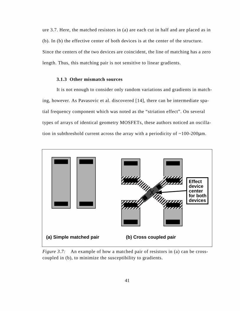
as in
.
zero
tch-
spa-
l
cilla-
s-
ure 3.7. Here, the matched resistors in (a) are each cut in half and are placed
(b). In (b) the effective center of both devices is at the center of the structure
Since the centers of the two devices are coincident, the line of matching has a
length. Thus, this matching pair is not sensitive to linear gradients.
3.1.3 Other mismatch sources
It is not enough to consider only random variations and gradients in ma
ing, however. As Pavasovic et al. discovered [14], there can be intermediate
tial frequency component which was noted as the “striation effect”. On severa
types of arrays of identical geometry MOSFETs, these authors noticed an os
tion in subthreshold current across the array with a periodicity of ~100-200µm.
Figure 3.7: An example of how a matched pair of resistors in (a) can be croscoupled in (b), to minimize the susceptibility to gradients.
X
Effectdevicecenterfor bothdevices
(a) Simple matched pair (b) Cross coupled pair
41

for
this
n
be
ber
sig-
a
rved
n
this
For
lec-
lso
re
ox-
The striation effect was as high as a 30% increase in the normalized current
pMOS devices and 7% for nMOS devices. It was proposed by Pavasovic that
may have resulted from the threshold adjust ion implantation. That is, if the io
implant current was too high, only a few or maybe one rasterscan pass would
needed to achieve the relatively low implant dose.
Dynamic mismatches are also possible. Tewksbury [18] outlined a num
of potential sources for dynamic parameter fluctuations in MOSFETs. A large
nal input that is typical for analog applications, across the gate and source of
MOSFET, can produce threshold voltage shifts. For instance, Tewksbury obse
a Vt shift of 500µV on an nMOS transistor after applying a 2V, 10msec pulse o
the gate. For a 5V pulse, the Vt shift was about 900µV. The Vt shift required about
200msec to disappear asymptotically. It was proposed that the mechanism for
shift was oxide trap charge exchanges in the gate oxide via direct tunneling.
large pulse times and/or voltages, mobile ion movement in the gate oxide, mo
ular dipole polarization, interface state charge trapping and self heating can a
cause parametric shifts and mismatches. These dynamic mismatch sources a
beyond the scope of this research.
3.2 Mismatch measures
3.2.1 Two device mismatch
Matching is the electrical comparison of two similar devices in close pr
imity. There are three statistics used to describe the mismatch between two
42
as
as
ica-
lat-
iven
,
devices: the difference, the percent difference, and the relative difference.
Throughout the rest of this paper the difference for a parameter, P, will be given
an operator, , the percent difference as , and the relative difference
. The parentheses are generally applied in instances of ambiguity. Appl
tion of the three statistics varies according to need, but generally voltage and
eral geometry mismatch is given as and the remaining parameters are g
as , or . For the sake of clarity, the three statistics are defined as
, (3.1)
, (3.2)
, (3.3)
Some useful mappings between the four statistics are,
(3.4)
(3.5)
(3.6)
and for the variances in the four statistics,
∆a P( ) ∆% P( )
∆r P( )
∆a P( )
∆% P( ) ∆r P( )
∆a P( ) P1 P2–=
∆% P( ) 100P1 P2–( )
P2-----------------------=
∆r P( )P1
P2------=
∆r P( )∆% P( )
100---------------- 1+=
∆r P( )∆a P( )
P--------------- 1+=
∆% P( ) 100∆a P( )
P---------------
=
43

n of
ion
ean.
fol-
alue
me
10)
(3.7)
(3.8)
(3.9)
It should be noted that the absolute difference is not used since the preservatio
the sign is important for observing gradient effects.
Several authors [9, 10, 11] have chosen to use a slightly different variat
on the percent difference statistic, which is the percent difference about the m
The percent difference about the mean is differentiated from Eq. (3.2) by the
lowing definition,
(3.10)
These two statistics are numerically equivalent estimates since the mismatch v
is much less than the nominal value of the parameter and they contain the sa
number of degrees of freedom. One degree of freedom is consumed by the
estimation of the expectation value in the denominator of Eq. (3.2) and Eq. (3.
and the other is included in the estimation of the deviation in the numerator.
σ∆rP2
σ∆%P2
10000---------------=
σ∆rP2
σ∆aP2
P2
------------=
σ∆%P2
10000σ∆aP
2
P2
------------=
MM 200P1 P2–( )P1 P2+( )
------------------------=
44

2.5,
ices
n,
ntly.
n
P
ject
t
for
3.2.2 Single device mismatch
As pointed out in the examples of Section 2.1, Section 2.4, and Section
matched devices can often include more than a simple pair. In Section 2.1, dev
in matched pairs may have dissimilar drawn geometries. For SPICE simulatio
the matching of each device in the matching pair(s) must be varied independe
This necessitates a different matching measure than the ones listed in Sectio
3.2.1.
Here, the notion of an expectation value for a given matched parameter,1,
is introduced. The mismatch between a device and its expectation value is,
(3.11)
where E(P) is the expectation of P. For a pair of devices,
(3.12)
where PMM here denotes that this is the mismatch for a pair of devices. The
mismatch definition about its expectation value as defined in Eq. (3.11) is sub
to the condition that E(P1) = E(P2) for identically drawn devices. This means tha
gradient effects must be accommodated aside from this definition of mismatch
a single device.
For identically drawn devices, E(P1) = E(P2) = E(P) so,
MMP E P( )–
E P( )----------------------=
PMM
P1 E P1( )–
E P1( )---------------------------
P2 E P2( )–
E P2( )---------------------------–=
45
e
ce
of
ny
e
me-
volt-
(3.13)
where E(P) can be estimated by P1, P2 or the mean of P1 and P2.
For dissimilar devices,
(3.14)
wheref is the matching model, given in relative units, G represents geometry
parameters, P is the proximity, OM is the matching orientation, OD is the device
orientation, and D is the extent of dummy devices. Rearranging Eq. (3.14),
(3.15)
Thus, P2 is normalized to P1 by the ratio of the expectation values. The differenc
between the normalized P2 and P1 can be used to fit the matching model.
It is apparent from Eq. (3.15) that mismatch is not limited to the differen
in performance for identically drawn devices. Mismatch is in fact a realization
intra-die variations. Not unlike the inter-die variations that are included in ma
statistically derived analysis such as [19], the intradie variations use the sam
POV and POD equations but with typically smaller distributions.
Caution should be exercised when combining devices of dissimilar geo
tries because the devices may be operating in different regions for the same
PMM
P1 P2–
E P( )------------------=
PMM
P1 E P1( )–
E P1( )---------------------------
P2 E P2( )–
E P2( )---------------------------–
P1
E P1( )---------------
P2
E P2( )---------------– f G P OM OD D, , , ,( )= = =
P1 P2
E P1( )E P2( )--------------- E P1( ) f G P OM OD D, , , ,( )+=
46

r a
gh
d the
sider-
hing
n of
en-
l-
age bias. For instance, a BJT will enter the high level injection region sooner fo
small emitter compared to a large emitter for the same voltage bias. In the hi
current regions, the mismatch in the external resistance become significant an
overall BJT mismatch appears to degrade. This point is addressed when con
ing the proposed regression approach in Section 3.5.
3.3 Propagation of Deviation and Propagation of Variance
There are two fundamental equations that are used throughout the matc
discussion. These are the Propagation of Deviation (POD) and the Propagatio
Variance (POV). The POD equation, also known as the sensitivity equation,
relates the deviations in the independent variables to the deviation in the dep
dent variables for a given point. For instance, y=g(x1,x2) is assumed. Then fo
lowing the proof from Paupolis [20],
(3.16)
where∆ is the offset from the mean in the ith point for the independent variables
x1 and x2 and the dependent variable y. Eq. (3.16) may be re-written as,
(3.17)
whereµ1 andµ2 are the mean values of x1 and x2. The expected value of g(x1,x2)
is,
∆yi ∆x1i x1∂∂y ∆x2i x2∂
∂y+=
g x1 x2,( ) g µ1 µ2,( ) x1 µ1–( )x1∂∂
g x1 x2,( ) x2 µ2–( )x2∂∂
g x1 x2,( )+ +=
47

s,
.
jus-
of
(3.18)
where f(x,y) is the multivariate normal probability density function (pdf) given a
(3.19)
The first moment,µ, of Eq. (3.18) can be calculated as
(3.20)
which is then used to find the second moment of Eq. (3.18),
(3.21)
where r is the correlation coefficient between x1 and x2.
Eq. (3.21) is also known as the propagation of variance (POV) equation
This entire derivation assumes linearity in the independent variables which is
tified due to the small variations in the process parameters and the proximity
E g x1 x2,( )[ ] g x1 x2,( ) f x1 x2,( ) x1d x2d∞–
∞∫∞–
∞∫=
f x x,( ) 1
2πσ1σ2 1 r2
–--------------------------------------
x1 µ1–( )2
σ12
-------------------------2r x1 µ1–( ) x2 µ2–( )
σ1σ2---------------------------------------------------–
x2 µ2–( )2
σ22
-------------------------+
2 1 r2
–( )-------------------------------------------------------------------------------------------------------------------------–
exp=
µg g µ2 µ2,( )
σ12
x12
2
∂
∂g x1 x2,( ) 2r σ1σ2 x1 x2∂
2
∂∂
g x1 x2,( ) σ12
x12
2
∂
∂g x1 x2,( )+ +
2------------------------------------------------------------------------------------------------------------------------------------------------------------+=
σy2
x1∂∂y
2
σx1
2
x2∂∂y
2
σx2
22rσx1
σx2 x1∂∂y
x2∂∂y
+ +=
48

since
etry
bles
.
by
t-
the
devices. Zero correlations amongst the independent parameters was assumed
the mismatch is modeled in terms of fundamental physical process and geom
parameters.
Although this derivation included only two independent variables, x1 and
x2, Eq. (3.20) and Eq. (3.21) can be generalized to include m dependent varia
and n independent variables using matrices,
(3.22)
where is a vector of variances for the m dependent variables,Σ is an (mxn)
matrix of the squared partial derivatives, and is a n element vector of the
independent parameter variances.
Figure 3.8 shows the concept of POV qualitatively. As described by Eq
(3.16) and Eq. (3.21), a deviation in the independent variable, x, is multiplied
the gradient, g1 or g2, to give the deviation in the dependent variable, y. Integra
ing over many deviations, as described by the dispersion in the pdf of x, gives
pdf in g1(x) or g2(x) as determined by the respective gradient, g1 or g2.
Y ΣX=
Y
X
49
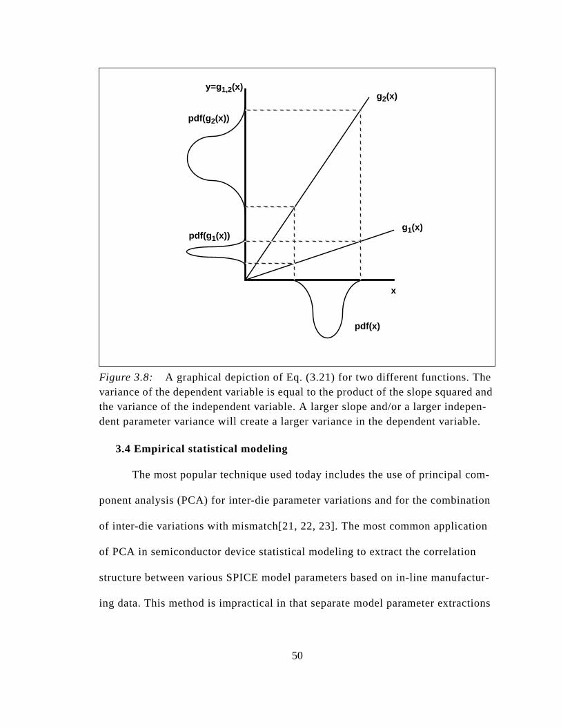
eand
en-le.
m-
tion
n
ctur-
ions
Figure 3.8: A graphical depiction of Eq. (3.21) for two different functions. Thvariance of the dependent variable is equal to the product of the slope squaredthe variance of the independent variable. A larger slope and/or a larger indepdent parameter variance will create a larger variance in the dependent variab
3.4 Empirical statistical modeling
The most popular technique used today includes the use of principal co
ponent analysis (PCA) for inter-die parameter variations and for the combina
of inter-die variations with mismatch[21, 22, 23]. The most common applicatio
of PCA in semiconductor device statistical modeling to extract the correlation
structure between various SPICE model parameters based on in-line manufa
ing data. This method is impractical in that separate model parameter extract
g1(x)
g2(x)
pdf(x)
pdf(g 2(x))
pdf(g 1(x))
x
y=g1,2(x)
50

ysis
l of
ap-
hap-
he
y
, or a
ram-
ter
he
an-
tical
uld
on-
need to be performed on each die that is sampled. Principal component anal
techniques are empirical and are reliant upon “happenstance” data.
Happenstance data are devoid of forced treatment combinations, typica
manufacturing data. At best, associative relationships may be gleaned from h
penstance data. Box, Hunter, Hunter [24] provide an excellent discussion on
penstance data which is applied to semiconductor statistical analysis here.
3.4.1 Inconsistent data
Inconsistent data refers to data that may have seen one-time shifts in t
process conditions over the lifetime of the sample. For example, a change ma
have occurred in the development time, the stepper focus /exposure settings
diffusion time/temperature. This offset is not representative of the process pa
eter variations.
3.4.2 Range of variables limited by control
A well known relationship could exist between a given process parame
and an important electrical parameter as depicted in Figure 3.9. However, if t
electrical parameter is important, process parameter will be well controlled in
manufacturing as denoted by the vertical bars in Figure 3.9. If data from the m
ufacturing line were examined, it would show the shaded data between the ver
bars. Looking at this data alone, no relationship would be evident and PCA wo
assign a very small, if any, component in this direction, leading to absent or n
51
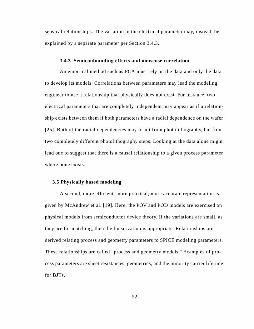
be
ata
ng
o
tion-
wafer
om
ght
meter
is
on
l, as
ters.
pro-
etime
sensical relationships. The variation in the electrical parameter may, instead,
explained by a separate parameter per Section 3.4.3.
3.4.3 Semiconfounding effects and nonsense correlation
An empirical method such as PCA must rely on the data and only the d
to develop its models. Correlations between parameters may lead the modeli
engineer to use a relationship that physically does not exist. For instance, tw
electrical parameters that are completely independent may appear as if a rela
ship exists between them if both parameters have a radial dependence on the
[25]. Both of the radial dependencies may result from photolithography, but fr
two completely different photolithography steps. Looking at the data alone mi
lead one to suggest that there is a causal relationship to a given process para
where none exists.
3.5 Physically based modeling
A second, more efficient, more practical, more accurate representation
given by McAndrew et al. [19]. Here, the POV and POD models are exercised
physical models from semiconductor device theory. If the variations are smal
they are for matching, then the linearization is appropriate. Relationships are
derived relating process and geometry parameters to SPICE modeling parame
These relationships are called “process and geometry models.” Examples of
cess parameters are sheet resistances, geometries, and the minority carrier lif
for BJTs.
52
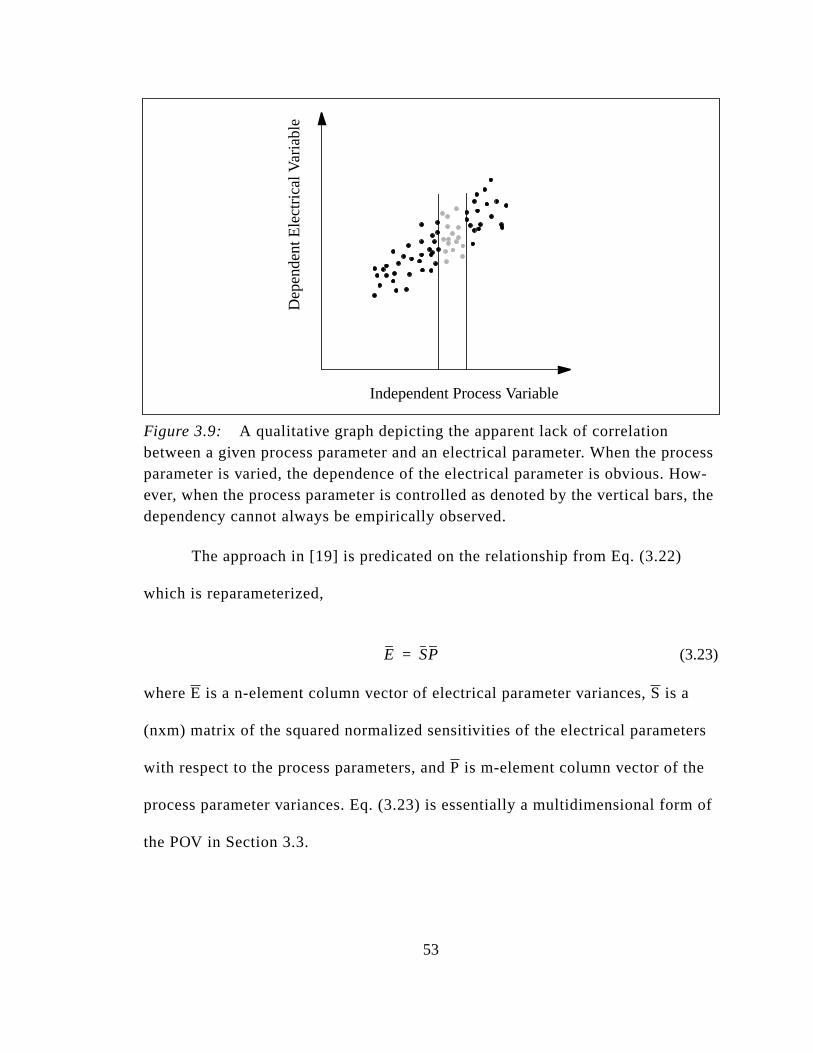
ocessow-, the
ers
m of
.
Figure 3.9: A qualitative graph depicting the apparent lack of correlationbetween a given process parameter and an electrical parameter. When the prparameter is varied, the dependence of the electrical parameter is obvious. Hever, when the process parameter is controlled as denoted by the vertical barsdependency cannot always be empirically observed.
The approach in [19] is predicated on the relationship from Eq. (3.22)
which is reparameterized,
(3.23)
whereE is a n-element column vector of electrical parameter variances,S is a
(nxm) matrix of the squared normalized sensitivities of the electrical paramet
with respect to the process parameters, andP is m-element column vector of the
process parameter variances. Eq. (3.23) is essentially a multidimensional for
the POV in Section 3.3.
Independent Process Variable
Dep
ende
nt E
lect
rical
Var
iabl
e
E SP=
53

is-
to
ed.
d a
re
lso
-
re
A MOSFET is used to demonstrate the application of this technique to m
match. In this case theE vector will contain values of Id mismatch over geometry
and bias combinations. TheP vector contains process parameter for which the
variances are unknown. This vector contains values such asσ∆L2, σ∆W
2, σtox2, and
channel dopant mismatch variance. The sensitivity matrix,S, contains the squared
sensitivities betweenP andE. These value can be determined numerically via
SPICE simulations about the nominal SPICE MOS model.E andS are known and
P needs to be solved which is linear regression solution.
3.6 Mismatch models
Three approaches have been used throughout the mismatch literature
derive matching models. Two of the techniques from Shyu are physically bas
These model the local and global random mismatch errors. Pelgrom performe
spatial frequency analysis. Although this technique is empirical, the results a
interesting in that they’re similar to the Shyu derivation. Pelgrom’s analysis a
provides a model for the systematic effects.
3.6.1 Mismatch model derivation from semiconductor device physics.
Two modeling approaches were developed by Shyu in the early publica
tions on mismatch. From [6, 7], referring to the local mismatch diagram in Figu
3.3 (a), the effective change in length is,
54
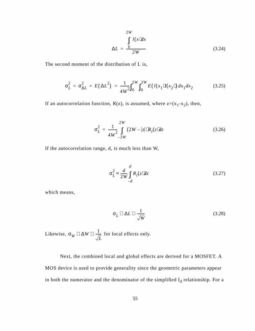
A
pear
(3.24)
The second moment of the distribution of L is,
(3.25)
If an autocorrelation function, R(z), is assumed, where z=(x1-x2), then,
(3.26)
If the autocorrelation range, d, is much less than W,
(3.27)
which means,
(3.28)
Likewise, for local effects only.
Next, the combined local and global effects are derived for a MOSFET.
MOS device is used to provide generality since the geometric parameters ap
in both the numerator and the denominator of the simplified Id relationship. For a
∆L
l x( ) xd
0
2W
∫2W
-----------------------=
σL2 σ∆L
2E ∆L
2 1
4W2
----------- E l x1( )l x2( ) x1 x2dd0
2W
∫0
2W
∫= = =
σL2 1
4W2
----------- 2W z–( )Rl z( ) zd
2W–
2W
∫=
σL2 d
2W-------- Rl z( ) zd
d–
d
∫≈
σL ∆L1
W---------∝ ∝
σW ∆W1
L-------∝ ∝
55

h,
all
MOSFET, , so, which implies, and for a
deviation in length produced by local effects,
(3.29)
Likewise, , so for a deviation in width produced by local effects,
(3.30)
Thus, the affect of local edge effects for a given parameter, P, is
(3.31)
where K is a constant coefficient for the local effects, , of length, L, and widt
W. Local area effects for P,
(3.32)
Referring to Figure 3.3(a), the global mismatch is a complete shift in the over
length by . For global edge effects, and ,
which is simply the POV.
I dWL-----∝
L∂∂I d W
L2
------∝ ∆I dW
L2
------∆L ∝ W
L2
---------=
∆I d
I d--------- 1
W L-------------∝
W∂∂I d 1
L---∝
∆I d
I d--------- 1
LW-------------∝
∆PP
-------KlL
L2W
-----------KlW
W2L
-----------+=
l
∆PP
-------KlLW
L2W
2--------------=
∆L σL ∆L KgL∝ ∝ σW ∆W KgW∝ ∝
56

In Shyu’s example [7], in saturation,
(3.33)
For a deviation in the gate length,
(3.34)
where is the model coefficient for the global effect, and for a deviation in
width,
. (3.35)
For a deviation in the gate charge, Q,
. (3.36)
For a deviation in the gate oxide, ,
. (3.37)
For a deviation in mobility,
. (3.38)
I d µCoxW2L------ Vgs Vt–( )2
=
∆I d
I d---------
KgL
L2
----------KlL
L2W
-----------+=
KgL
∆I d
I d---------
KgW
W2
-----------KlW
W2L
-----------+=
∆I d
I d---------
1Cox Vgs Vt–( )----------------------------------- KgQ
KlQ
WL---------+=
tox
∆I d
I d---------
1tox------- 1 2Q
Cox Vgs Vt–( )-----------------------------------+
Kgt
Klt
WL--------+=
∆I d
I d---------
1µ--- Kgµ
KlµWL---------+=
57

d
ble
nly
c-
ned
led
ja-
If we assume a Poisson distribution, , , , an
in general,
(3.39)
Local and global effects are parametrically similar. They are only distinguisha
for very small geometries (i.e. geometry ~ autocorrelation distance). Hence, o
global random effects are considered.
Lakshmikumar limited the analysis to the global effects. A point of distin
tion should be noted in the Lakshmikumar paper. Here global variation is defi
as, “variation [...] across a wafer or batch,” whereas local variation (also labe
as “mismatch”) is, “the variation in a component value with reference to an ad
cent component on the same chip.”
Again in saturation, the POV of the simple MOSFET Id relationship is,
(3.40)
where,
(3.41)
Using POV,
σµ2 1
LW---------∝ σtox
2 1LW---------∝ σQ
2 1LW---------∝
∆PP
-------KlL
L2W
-----------KlW
W2L
-----------KlLW
L2W
2--------------
KgL
L2
----------KgW
W2
-----------KgLW
LW--------------+ + + + +=
σI d
2
I d2
--------σβ
2
β2------ 4
σVT
2
Vgs Vt–( )2----------------------------
4r σVtσβ
β Vgs Vt–( )-----------------------------–+=
VT φMS 2φB
QB
C-------
Qf
C-------–
qDI
C---------+ + +=
58
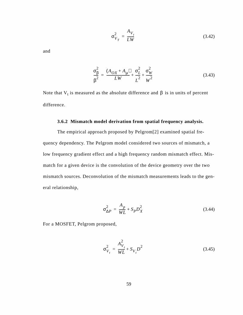
t
h, a
Mis-
o
gen-
(3.42)
and
(3.43)
Note that Vt is measured as the absolute difference and is in units of percen
difference.
3.6.2 Mismatch model derivation from spatial frequency analysis.
The empirical approach proposed by Pelgrom[2] examined spatial fre-
quency dependency. The Pelgrom model considered two sources of mismatc
low frequency gradient effect and a high frequency random mismatch effect.
match for a given device is the convolution of the device geometry over the tw
mismatch sources. Deconvolution of the mismatch measurements leads to the
eral relationship,
(3.44)
For a MOSFET, Pelgrom proposed,
(3.45)
σVT
2AVt
LW---------=
σβ2
β2------
AOX Aµ+( )LW
-----------------------------σL
2
L2
------σW
2
W2
--------+ +=
β
σ∆P2 Ap
WL-------- SPDX
2+=
σVt
2AVt
2
WL--------- SVt
D2
+=
59
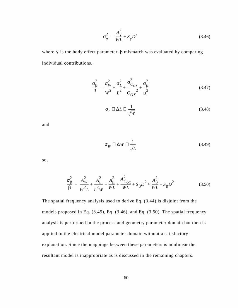
ncy
n is
(3.46)
where is the body effect parameter.β mismatch was evaluated by comparing
individual contributions,
(3.47)
(3.48)
and
(3.49)
so,
(3.50)
The spatial frequency analysis used to derive Eq. (3.44) is disjoint from the
models proposed in Eq. (3.45), Eq. (3.46), and Eq. (3.50). The spatial freque
analysis is performed in the process and geometry parameter domain but the
applied to the electrical model parameter domain without a satisfactory
explanation. Since the mappings between these parameters is nonlinear the
resultant model is inappropriate as is discussed in the remaining chapters.
σγ2 Aγ
2
WL-------- Sγ D
2+=
γ
σβ2
β------
σW2
W2
--------σL
2
L2
------σCOX
2
COX2
--------------σµ
2
µ2------+ + +=
σL ∆L1
W---------∝ ∝
σW ∆W1
L-------∝ ∝
σβ2
β------
AW2
W2L
-----------AL
2
L2W
-----------Aµ
2
WL--------
ACOX
2
WL------------- SβD
2+ + + +
Aβ2
WL-------- SβD
2+≈=
60

ally
t geo-
rn
ure
el-
etry
nif-
cu-
ide
log
ng,
e
in
3.6.3 Statistical analysis of the three modeling approaches
Each of the three modeling techniques yield models that are parametric
similar. They are only different for small lengths and/or small widths. In the
papers that present each of the three techniques, none of them had sufficien
metric sampling, particularly for small lengths and widths, to adequately disce
the perimeter mismatch contributions. Figure 3.10 (a), Figure 3.11 (a), and Fig
3.12 (a) show the geometric samplings from Shyu [7], Lakshmikumar [8], and P
grom [2] respectively. Plots of the prediction variance versus the inverse geom
space is shown in Figure 3.10 (b), Figure 3.11 (b), and Figure 3.12 (b). The sig
icance of poor geometric sampling is evident in these plots. A high prediction
variance implies low confidence in the predicted value from the model. In parti
lar, the poorest coverage is in the areas of long, narrow devices, and short, w
devices. These two regions are critical for two reasons. First, in MOSFET ana
design, short, wide devices are desirable for their high transconductance. Lo
narrow MOS devices are likewise needed for their high output resistances. Th
second reason why these regions are important is that these are the regions
which the global and local effect are most distinguishable.
61

Figure 3.10: A plot of the experimental design (a) and prediction variance (b)from Shyu [7].
Figure 3.11: A plot of the experimental design (a) and prediction variance (b)from Lakshmikumar [8].
0.04
0.03
0.02
0.01
1/Length (1/u)
0.040.03
0.020.01
1/Width (1/u)
Predicted Var.
0.26
4.51
8.76
13.01
Wi
dt
h(
u)
0
10
20
30
40
50
60
70
80
90
100
Length (u)0 10 20 30 40 50 60 70 80 90 100
(a) Geometric sampling (b) Prediction variance
PredictionVariance
Wid
th [µ
m]
Length [µm]
(a) Geometric sampling (b) Prediction variance
Wi
dt
h(
u)
0
10
20
30
40
50
Length (u)0 10 20 30 40 50
0.333
0.250
0.167
0.083
1/Length (1/u)
0.1670.118
0.0690.021
1/Width (1/u)
Predicted Var.
0.11
2.78
5.46
8.13
PredictionVariance
Wid
th [µ
m]
Length [µm]
62

b)
e fac-
tch
Figure 3.12: A plot of the experimental design (a) and prediction variance (b)from Pelgrom [2]. One point (W=700, L=10) from Pelgrom’s paper is excludedfrom this plot since it will little consequence on this prediction variance plot in (and because it will distort these plot significantly.
3.7 Mismatch experimental design.
The first step to defining a matching experimental design is to identify
those factors that affect matching and the appropriate response variables. Th
tors are common between the four types of devices that are discussed. The
response variables are handled separately for each device.
3.7.1 Mismatch factors
Layout considerations that affect matching are:
• Geometry - As noted in Section 3.6, the random component of misma
improves with increasing geometry.
(a) Geometric sampling (b) Prediction variance
Wi
dt
h(
u)
0
10
20
30
Length (u)0 10 20 30 0.625
0.433
0.242
0.050
1/Length (1/u)
0.4170.292
0.1670.042
1/Width (1/u)
Predicted Var.
0.04
3.07
6.11
9.15
PredictionVariance
Length [µm]
Wid
th [µ
m]
63

g of
the
S-
of
on-
led
e
e
• Proximity - Proximity is the physical separation distance between
matched devices. Proximity is measured as the center-to-center spacin
the devices. For a resistor, the proximity is measured from the center of
resistor body, for a capacitor, from the center of the capacitor, for a MO
FET, from the center of the gate and for a vertical BJT, from the center
the emitter.
• Matching orientation - This represents the orientation of the line that c
nects the center of the device in a matched pair(s). This line is thus labe
as the “line of matching”. Various lines of matching are shown in Figure
3.13 for a matched BJT pair. Matching orientation can be measured in
degrees with reference to the wafer flat or notch.The combination of th
proximity and matching orientation factors are used to detect gradient
effects.
Figure 3.13: Variations on matching orientation. The arrows represent the “linof matching”.
(a) (b) (c)
64
en-
of
n
nder
f the
gy,
r-
et-
th
-
ric
• Device orientation - This orientation refers to the orientation of each
device in a matching pair with respect to the wafer flat or notch. Figure
3.13 shows several examples of varying device orientations. Device ori
tation can be important for mismatch for two reasons. The effective mass
free carriers (and hence mobility) is a weak function of orientation whe
the matched structure is in a low stress state. When a device is placed u
stress, the stresses on the crystal lattice changes the effective mass o
carriers through the relationship,
(3.51)
where is the carrier effective mass, h is Planck’s constant, E is ener
and k is the momentum vector.
A second implication of device orientation results from a non-no
mal ion implantation (I/I) angle to the wafer surface. In order to obtain b
ter control of the I/I implantation depth and straggle (spread in the dep
direction), wafers are implanted with a 7o tilt on the wafer, which mini-
mizes the channelling effect [26]. For certain devices, such as the MOS
FET, the angled implant will create a shadowing effect as depicted in
Figure 3.14. In Figure 3.14(a), the source/drain regions will be symmet
if the implant angle is 0o or if the 7o implant angle is given with respect to
m∗ h2
4π2
k2
2
d
d E
------------------------=
m∗
65

ill
me
the page surface. But in Figure 3.14(b), there will be a asymmetric
encroachment of either the source or the drain under the gate, which w
cause a shadow of the implant by the polysilicon gate. The result of the
shadowing is a mismatch offset for the layout schemes shown in Figure
3.15(a) and Figure 3.15(b) despite the fact that both layout have the sa
line of matching.
Figure 3.14: The effect of ion implantation shadowing in (b) versus a 0o implantin (a).
Figure 3.15: Variations on device orientation. All three combinations have thesame matching orientation.
(a) (b)
0o Implant 7 o Implant
(a) (b)
GateSource
Line ofmatching
Drain Drain Line ofmatching
Gate
GateDrain
Dra
in
Source
Sou
rce
66

ari-
/W
rs
is
the
e
oise
by
ce
sing
3.7.2 Mismatch DOE.
If it is assumed for a moment that all matching parameters (response v
ables) can be modeled with the generic mismatch model,
, (3.52)
a modified 32 factorial experimental design can be used with factors 1/L and 1
and include the interaction term, . Three levels are chosen for both facto
since it is necessary to detect deviations from 1/geometry trend. This is
particularly true for those terms that contain the device width since mismatch
not guaranteed to monotonically decrease with increasing width. This is
applicable in the case where the matched pair is laid out such that increasing
device width would increase the center-to-center spacing of the devices, as
pointed out in Section 3.1. This confounded effect is also possible between th
spacing and the length if the device orientation is rotated by 90o, but the
orientation of the line of matching remains the same. A deviation from the
1/geometry trend can also be an indicator of hitting the measurement system n
floor.
The four geometric corners of the experimental design are established
the minimum length and width and some “large” length and “large” width. Sin
the small signal component of mismatch asymptotically decreases with increa
PMM1
L2
------ 1
W2
-------- 1LW---------+ +=
1
LW-------------
67

t
ter
sid-
s-
cts.
ter-
ce
to
ence
o
ari-
ition
r-
geometry, the exact value of “large” geometries is not important provided tha
either the asymptotic trend is sufficiently sampled or the range of anticipated
geometries is sufficiently covered. For a 3 level experimental design, the cen
point should be placed half way between the two extremes. This means that
(3.53)
but can be reduced,
if (3.54)
where G is the given geometry parameter (either length or width).
A final requirement for the geometric sampling for mismatch is the con
eration of gradient effects. If all devices are placed at minimum separation di
tance, the width dependence will be highly confounded with the gradient effe
This effect is shown in Figure 3.16. Figure 3.16(a) and (b) depict how the cen
to-center spacing (a.k.a. proximity) of the two devices increase with width. Sin
it was established in Section 3.1.2 that the susceptibility of the matching pair
gradients is dependent on the center-to-center spacing this implies a depend
on the device width as shown in Figure 3.16 (c). This means that there are tw
geometric regimes for matching; one region is dominated by the small signal v
ations and the other by gradient effects. Figure 3.16 (d) shows how the trans
from the former regime to the latter can negatively impact the matching perfo
Gcenter 2Gl earg Gmin
Gl earg Gmin+----------------------------------=
Gcenter 2Gmin≈ Gl earg Gmin»
68
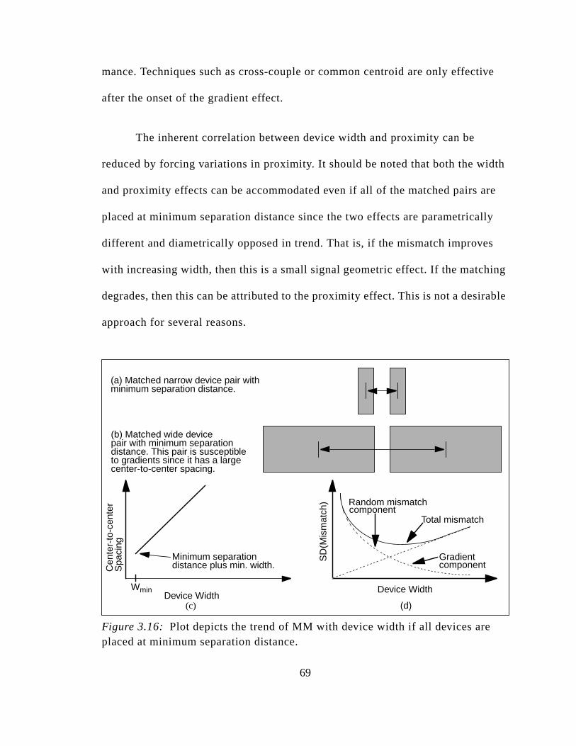
ive
dth
re
lly
s
ng
ble
mance. Techniques such as cross-couple or common centroid are only effect
after the onset of the gradient effect.
The inherent correlation between device width and proximity can be
reduced by forcing variations in proximity. It should be noted that both the wi
and proximity effects can be accommodated even if all of the matched pairs a
placed at minimum separation distance since the two effects are parametrica
different and diametrically opposed in trend. That is, if the mismatch improve
with increasing width, then this is a small signal geometric effect. If the matchi
degrades, then this can be attributed to the proximity effect. This is not a desira
approach for several reasons.
Figure 3.16: Plot depicts the trend of MM with device width if all devices areplaced at minimum separation distance.
(a) Matched narrow device pair withminimum separation distance.
(b) Matched wide devicepair with minimum separationdistance. This pair is susceptibleto gradients since it has a largecenter-to-center spacing.
Cen
ter-
to-c
ente
rS
paci
ng
Minimum separationdistance plus min. width.
Device WidthDevice Width
(c) (d)
Wmin
SD
(Mis
mat
ch) Random mismatch
component
Gradientcomponent
Total mismatch
69

pred-
reat-
in
ween
evi-
the
t
pa-
e
ed
ch-
as
g,
nd
hip,
First, the sampling is parametrically different. It was established earlier
that the anticipated sampling for the small signal geometric dependence was
icated on an asymptotic monotonic decrease in matching with geometry. The t
ment combinations of the experimental design were placed at equal intervals
the inverse geometry space which means that there is a large separation bet
the center geometry and the large geometry. If the proximity effect becomes
dent within this region, the estimation of the gradient will be based solely on
large geometry since there is a mandatory zero intercept term for any gradien
effect. Alternatively, the gradient effect may not be evident except for large se
ration distances that far exceed the region of practical geometries.
Second, fitting the models for proximity and width is akin to fitting a plan
about the line in Figure 3.16(c). Proximity and geometry samples can be plac
only above this line. Given a choice of the infinite number of points above this
line, the proximity and geometry combination with the most leverage is a mat
ing pair with minimum width and large proximity. Since the objective of this
device is to measure the gradient effect, the small signal mismatch should be
small as possible. This means that a long device should be chosen due to its
inverse length and inverse area dependencies. Along those same lines, a lon
wide matching pair will further reduce the small signal matching component a
may provide better insight into the proximity effect. Those factors limiting the
extent of proximity values are interconnect parasitics, layout area on the test c
and exceeding the linear region of the gradient effect.
70

f
n be
en-
or the
oxim-
he
vice
ed to
. It
a-
is-
ced
.
ions,
is
on-
Third, proper modeling of the gradient effect requires an examination o
both the mean and the standard deviation of the mismatch. Since a gradient ca
observed in either the mean or the standard deviation, the mean should be
included in the analysis.
Fourth, there are several types of partially determined functional depend
cies to be considered. These effects are labeled as gradients here because f
purposes of analog design, matched devices are placed in relatively close pr
ity. As such, regardless of the functionality of the partially determined trend, t
trend can reasonably be assumed to be linear within the realm of practical de
separations in analog design. However, special device placings may be need
accommodate oscillatory effects of various periodicity and/or nonlinear trends
is anticipated that the mismatch of largely separated devices will become of
increased interested, particularly as the concept of mismatch (or intradie vari
tion) modeling becomes of greater interest to digital circuits. The impact of m
match on clock skew for instance, will mean that matched devices could be pla
on opposite sides of a die that contains millions of transistors.
Fifth, gradients can and will have components in both lateral directions
This means that separated devices need to be placed in two orthogonal direct
not just in the direction of the width.
The modified 32 factorial experimental design in inverse geometry space
given in Figure 3.17(a). The plot of the prediction error in Figure 3.17(b) dem
71
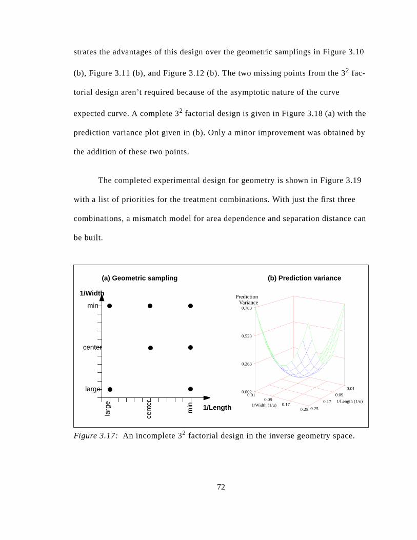
3.10
by
19
e can
strates the advantages of this design over the geometric samplings in Figure
(b), Figure 3.11 (b), and Figure 3.12 (b). The two missing points from the 32 fac-
torial design aren’t required because of the asymptotic nature of the curve
expected curve. A complete 32 factorial design is given in Figure 3.18 (a) with the
prediction variance plot given in (b). Only a minor improvement was obtained
the addition of these two points.
The completed experimental design for geometry is shown in Figure 3.
with a list of priorities for the treatment combinations. With just the first three
combinations, a mismatch model for area dependence and separation distanc
be built.
Figure 3.17: An incomplete 32 factorial design in the inverse geometry space.
1/Width
1/Length
min
min
large
larg
e
cent
er
center
0.25
0.17
0.09
0.01
1/Length (1/u)
0.250.17
0.090.01
1/Width (1/u)
Predicted Var.
0.002
0.263
0.523
0.783
(a) Geometric sampling (b) Prediction variance
PredictionVariance
72

ederse
re-’s”tions
Figure 3.18: A complete 32 factorial design in inverse geometry space as viewfrom the non-inverted geometry space (a). The predicted variance versus invgeometry (b).
.
Figure 3.19: An example experimental design for device geometries. Dots repsent the minimum spaced pairs at various geometry configurations and the “Xrepresent spaced pairs. Spaced pairs should be spaced in two orthogonal direcon the wafer to observe gradients in all directions.
(a) Geometric sampling (b) Prediction variance
Wi
dt
h(
u)
0
10
20
30
40
50
60
70
80
90
100
Length (u)0 10 20 30 40 50 60 70 80 90 100
0.25
0.17
0.09
0.01
1/Length (1/u)
0.250.17
0.090.01
1/Width (1/u)
Predicted Var.
0.002
0.240
0.477
0.715
PredictionVariance
Width
Length
min2*min
min
2*m
in
large
larg
e
Priority Length Width Spacing
1 min min min2 large large min3 large large large4 2*min 2*min min5 2*min min min6 min 2*min min7 large min min8 min large min9 large min large
73

the
ting
re
led
gth
tor
Chapter 4 Resistor Mismatch
4.1 Prior work
Not much is published for the mismatch of resistors, presumably due to
relative simplicity of the devices. However, resistors serve as an excellent star
point for mismatch analysis since both the geometric and bias relationships a
simple.
4.2 Method
Both diffused and polysilicon resistors are covered in this chapter.
4.2.1 Dielectrically isolated resistor
Dielectrically isolated resistors, such as polysilicon and metal, are mode
by the relationship,
(4.1)
where and are the drawn length and width. and account for the
difference between the drawn length and width and the effective electrical len
and width. ρs is the sheet resistance, Rcon is the contact resistance component
(units of ohms/µm) and Rend is the end resistance component, including the
spreading resistance. As a matter of practice, ~ . Rcon and Rend are
parametrically similar to which means that Rcon and Rend can be modeled
through , the end resistances can be modeled as an additions to the resis
RL' ∆L+( )
W' ∆W+( )---------------------------ρs
2Rcon
W---------------
2Rend
W---------------+ +=
L' W' ∆L ∆W
W' ∆W+( ) W
∆L
∆L
74

be
ry
s a
the
the
ance
into
length. Combining these resistances removes some of the physical meaning
behind , but this model suffices for predicting the resistance. Eq. (4.1) can
reparameterized to,
(4.2)
since the variation of the effective length and width, L and W, is the same as
and respectively.
The mismatch of R in Eq. (4.2) is caused by mismatches in the geomet
and sheet resistance which leads to the POV relationship,
(4.3)
whereσ2L is the variance of L,σ2
W is variance of W,σ2ρs is the variance ofρs
and r is the correlation coefficient between L and W. The sheet resistance ha
Poisson distribution. The probability that an individual dopant atom resides in
resistor body is small but the number of dopant atoms is large. A Poisson
distribution has a variance that is inversely proportional to the mean value. As
area of the resistor increases, the variability of the resistor due to sheet resist
decreases which allows the third and fourth terms in Eq. (4.3) to be combined
a single 1/(LW) term yielding,
∆L
RL' ∆L+( )
W' ∆W+( )---------------------------ρs
LW-----ρs= =
L' ∆L+( ) W' ∆W+( )
σ∆%R2 σR
2
R2
------σL
2
L2
------σW
2
W2
--------2σLσWrLW
LW-----------------------------
σρs2
ρs2
--------+ + += =
75

he
rms
.1.
ce
the
ial
se,
(4.4)
where is the estimated variance of the resistance mismatch. Note that t
model parameters, , and have been re-named from the variance te
in Eq. (4.3) since these parameters are estimated composite parameters.
Additional terms, and can be added to the resistor mismatch model to
account for gradient effects, which can contribute to the mismatch,
. (4.5)
Coefficients and are estimated based on resistor pairs spaced with
orthogonal proximities, and .
4.2.2 Monosilicon (diffused) resistor
Monosilicon resistors are more complicated to model than dielectrically
isolated resistors because of the well bias dependence, as shown in Figure 4
Here, an increase in the reverse bias junction potential increases the resistan
because of the encroachment of the junction depletion region into the body of
resistor. As soon as a bias is placed from source to drain, the junction potent
varies across the length of the resistor and the resistor is “pinched”. In this ca
the resistor mismatch is calculated from the “zero bias” resistance.
s∆%R2 sL
2
L2
------sW2
W2
--------sLW2
LW----------+ +=
s∆%R2
sL2
sW2
sLW2
dX dY
s∆%R2 sL
2
L2
------sW2
W2
--------sLW2
LW---------- dX
2SX
2dY
2SY
2+ + + +=
dX dY
SX SY
76

the
ses.
to
a-
f a
etal
so
nce
pro-
e
Figure 4.1: Example cross section diagram of a diffused resistor.
The zero bias resistance is the extrapolated resistance for zero volts across
resistor terminals and the well, as measured from several applied non-zero bia
For typical diffused resistors, the well induced pinch-off voltage is around -100
-1000V which makes the resistor mismatch dependence on the backgate bias
negligible.
4.3 Test structures
To obtain the required accuracy and precision for resistor matching me
surements, the resistors need to have Kelvin metal contacts. The accuracy o
non-Kelvin resistance measurement is compromised because of the added m
resistance in the interconnect. Even if the interconnects are carefully laid out
that both resistors contain symmetric interconnects, the precision of the resista
measurements and hence the accuracy of the mismatch measurement is com
mised because the metal interconnects are also resistors and will also involv
Field
Drain
Depletion RegionEncroachment
DiffusedResistor
PinchedResistance
Source
ILD0
Metal
Oxide
Metal
Well Contact Metal
77

ded
ay.
own
volt-
essen-
tal
tal
s the
om
con-
inherent mismatches. Although the metal resistance is much lower than the
intended resistor, the metal resistance mismatch can be larger than the inten
resistor test structure due to the granularity of metal thin films.
There are several ways to layout Kelvin matching resistors in a pad arr
The first, a “full Kelvin” is shown in Figure 4.2(a). Here a “common Kelvin” is
run through each of the devices from pads 9 to 16. The three resistor pairs sh
would contain various length and width combinations as determined from an
experimental design. The force potential can be applied to either pad and the
age just above the resistor contact is sensed by the other pad. The sense pad
tially uses a high resistance voltmeter to prevent current flow through the me
interconnect. Without current flow, there is no I-R voltage drop across the me
interconnect.
For example, in order to measure the left-most R1 resistor in Figure 4.2(a),
a force voltage, or current, is applied to pads 1 and 16. The voltage drop acros
resistor can be measured from pads 2 and 9. Since there is no current flow fr
pads 2 to 9, the only voltage drop that is measured is from the resistor and its
tacts.
78
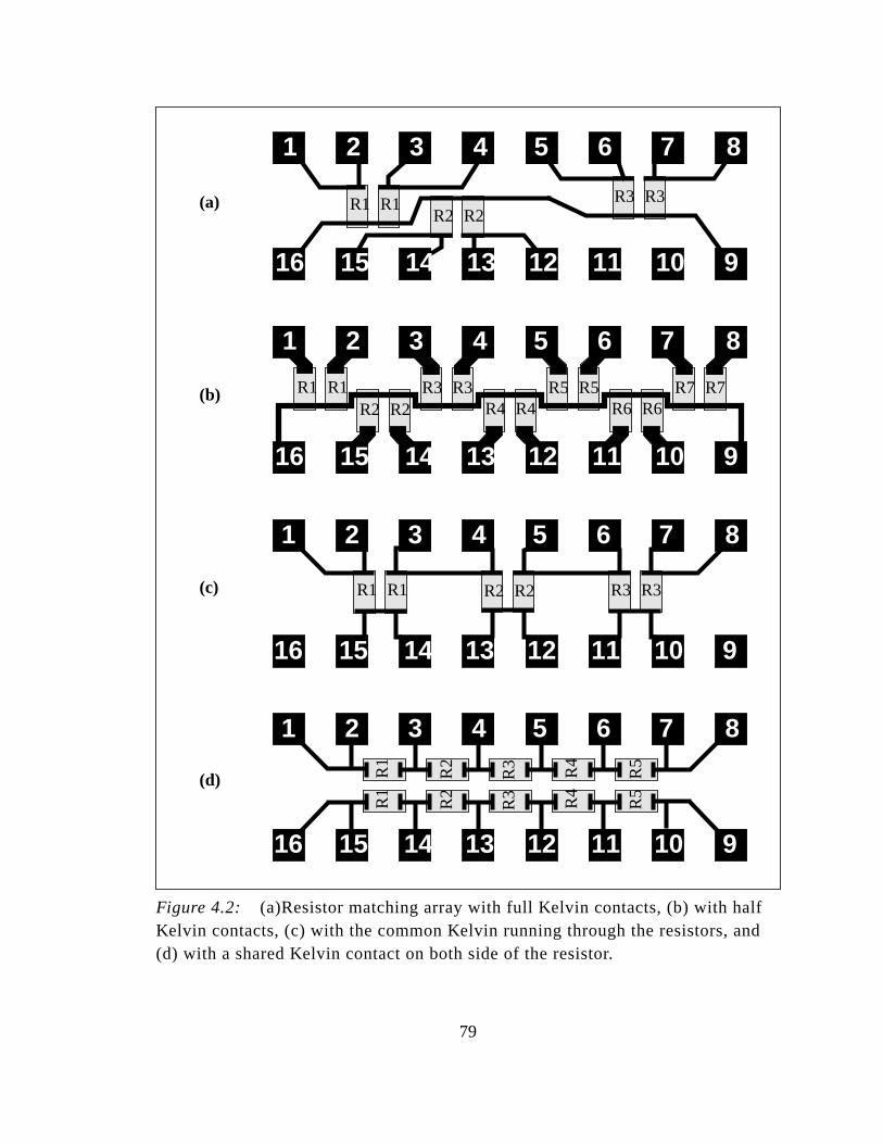
d
Figure 4.2: (a)Resistor matching array with full Kelvin contacts, (b) with halfKelvin contacts, (c) with the common Kelvin running through the resistors, an(d) with a shared Kelvin contact on both side of the resistor.R1 R1R2 R2
R3 R3
1 2 3 4 5 6 7
10111213141516
8
9
R1 R1R2 R2
R3 R3R4 R4
R5 R5R6 R6
R7 R7
1 2 3 4 5 6 7
10111213141516
8
9
R1 R1 R2 R2 R3 R3
1 2 3 4 5 6 7
10111213141516
8
9
R1
R1
R2
R2
R3
R3
1 2 3 4 5 6 7
10111213141516
8
9
R4
R4
R5
R5
(a)
(b)
(c)
(d)
79

sis-
-
in
s
to
and
or
is
l
re is
of
use
since
If the metal resistance on the short, non-common, Kelvin side of the re
tor is small compared to the resistor, the “short Kelvin” can be removed to pro
duce a more compact test structure as shown in Figure 4.2(b). The resistors
Figure 4.2(b) have about 3 squares of metal at an assumed typical value of
30mΩ/square. A prober contact resistance is typically about 0.5Ω. This means that
the parasitic resistance of the measurement is about 0.6Ω. To maintain a minimum
parasitic offset of 0.1%, the half Kelvin array should only be used for resistor
greater than 600Ω.
Caution should be exercised when using the array in Figure 4.2(b) due
the mismatch error incurred from the metal resistance, the prober resistance,
the switching matrix if an auto-prober is used. The same SMU (Source/Monit
Unit) can be used for both devices in the matching pair.
The third implementation in Figure 4.2(c), is similar to the first resistor
matching array. The common Kelvin is routed through the resistor bodies. Th
configuration still requires two pads for the common Kelvin and two additiona
pads per resistor. This approach has been used by Larsen et al. in [31], but the
no apparent advantage to this structure over the one in Figure 4.2(a) in terms
the pad consumption. The added resistance in the common Kelvin line could ca
heating problems if used for the force pads and could cause larger debiases
since the common Kelvin resistor chain has a larger resistance.
80

e
tic
,
ent.
one
om-
ric
er to
ctors
e.
ge
nter-
ross
two
e is
rce
A fourth approach is given in Figure 4.2(d). This layout is efficient in th
pad utilization and the resistors are near Kelvin. Only a small piece of parasi
metal that is not Kelvin produces an offset in mismatch. The probe resistance
contact resistance, and the switch matrix can be removed from the measurem
For diffused resistors, one pad is needed for a well contact. Since only
resistor is biased at a time while the other resistors are left floating, all of the
resistors in a given array and for a given type (n-type vs. p-type) can share a c
mon tub/back-gate.
Dielectrically isolated resistors are also thermally isolated. Most dielect
resistors usually have a low sheet resistance and require large currents in ord
generate a sufficient voltage drop across the resistor to measure. These two fa
often lead to self heating in the resistor and thermal changes in the resistanc
Therefore bias levels should be limited by power dissipation constraints.
Low value resistors can also lead to biasing problems. If the force volta
is large enough to supply large currents through the metal interconnects, the i
connects can heat and shift the resistor values. Also, the I-R voltage drop ac
the interconnect can create a significant offset in the sense voltage across the
resistors in a pair. This is especially true for spaced resistor pairs in which ther
significant metal interconnect offset between the two devices. In this case, a fo
current should be used in order to produce the desired target sense voltage.
81

rs
dy.
y.
om
was
As a matter of practice, with multi-layer metal processes, metal resisto
should contain interconnects using a different metal layer than the resistor bo
In this way, the via resistance and mismatch is included with the resistor bod
4.4 Measurements
Mismatch data was collected on five different types of diffused resistors
from a 0.8µm power BiCMOS technology. Details of these three resistors are
given in Table 4.1.
Table 4.1: Five types of resistors (A, B, C, D, and E) from a 0.8µm powerBiCMOS technology.
Mismatch data was collected on 17 die sites of a single wafer. Results fr
a previous study on a similar technology had shown that a one wafer sample
Parameter Resistor A Resistor B Resistor C Resistor D Resistor E
Dopant type n n p p p
Sheet resistance(ohms/sq)
51.3 732.6 89.6 876.14 4627.8
Junction Depth(µm)
0.325 0.6 0.425 0.85 2.5
Target surfacedopant conc.
(cm-3)
5.0e19 3.3e17 3.0e19 8.0e17 3.0e16
Target peakdopant conc.
(cm-3)
1.3e20 5.0e17 6.0e19 1.0e18 5.0e16
Min length(µm)
1.6 2.0 1.6 2.0 2.8
Min width (µm) 0.8 0.8 0.8 0.8 5.6
82

stan-
hed
ily
y in
n
a
for
ppli-
try.
tch
tch
e
tar-
the
an adequate for predicting the mismatch across multiple wafers and lots. The
dard deviation of the percent difference between the two devices of each matc
pair versus the resistor geometry for resistor B is give in Figure 4.3. It is read
apparent that the mismatch improves asymptotically with increasing geometr
this figure as anticipated from Eq. (4.5). The fitted model for resistor B is give
by,
(4.6)
A comparison of this fit is given in Table 4.2. The other four resistors maintain
similar quality in the fit. A 3-dimensional plot of the model is shown in Figure
4.5. 3-dimensional plots for the devices B, C, D and E are given in Figure 4.4
through Figure 4.8.
The three-dimensional plots in Figure 4.4 through Figure 4.8 are useful
conceptualizing the mismatch surface, but they are less practical for design a
cations where one may need to extract the mismatch value for a given geome
Thus, three additional mismatch plots are proposed for presenting the misma
model. The first of these is shown in Figure 4.9 for resistor B where the misma
versus length is plotted for various widths. This plot is particularly useful sinc
designers often choose the width first, and then determine the length to fit the
get resistance. The plot of mismatch versus length for families of width can
become crowded for resistors in which there is much more contribution from
s∆%R2 0.1523
LW( )---------------- 0.01703
L2( )
------------------- 0.0003878
W2( )
------------------------- 2.488x10⁸–SX
28.204x10
8–SY
2+ + + +=
83

D in
re
s-
ca-
t of
it
ard
Not
4.4
for
t in
-
sep-
length dependence than from the width dependence such as resistors C and
Figure 4.6 and Figure 4.7. The family of curves for resistor C is shown in Figu
4.10. For this reason, a complimentary plot can be generated in which the mi
match is plotted against the resistor width for a family of resistor lengths as in
Figure 4.11.
The third plot is an adaptation of a popular plot in many mismatch publi
tions of the standard deviation of the mismatch versus the inverse square roo
the device area. This plot is based on the work from Pelgrom et al. [2] where
was proposed that the standard deviation of all electrical parameters scale
inversely with the square root of the area. In this situation, a plot of the stand
deviation of the mismatch versus 1/sqrt(area) should produce a straight line.
all resistor areas are equivalent in terms of the mismatch as shown in Figure
through Figure 4.8. The plot in Figure 4.12 demonstrates this.
Figure 4.12 shows the plot of mismatch versus inverse square root area
three different cuts in the three dimensional plot in Figure 4.5, L=W, L=Lmin, and
W=Wmin. In this plot, the three cuts are relatively closely spaced since the plo
Figure 4.5 is fairly symmetric and > in Table 4.3. For a highly non-sym
metric case, such as Figure 4.7 where > the three curves have a larger
aration as in Figure 4.13.
sLW2
sL2
sL2
sLW2
84
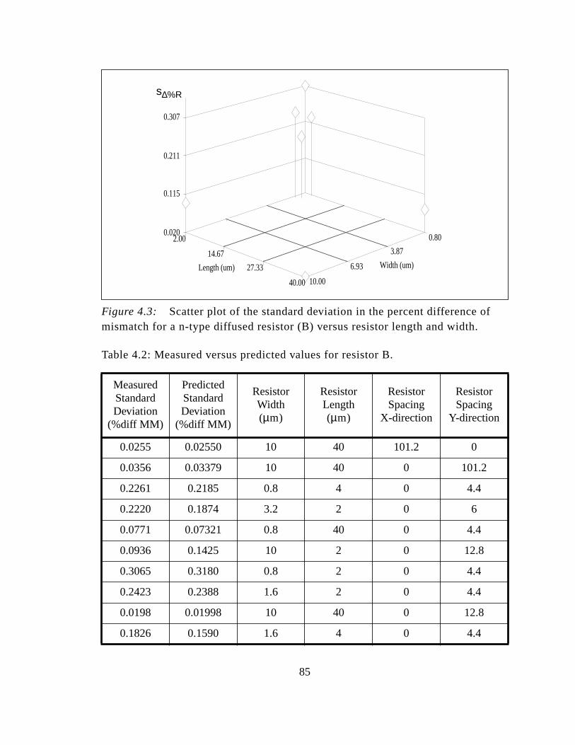
Figure 4.3: Scatter plot of the standard deviation in the percent difference ofmismatch for a n-type diffused resistor (B) versus resistor length and width.
Table 4.2: Measured versus predicted values for resistor B.
MeasuredStandardDeviation
(%diff MM)
PredictedStandardDeviation
(%diff MM)
ResistorWidth(µm)
ResistorLength(µm)
ResistorSpacing
X-direction
ResistorSpacing
Y-direction
0.0255 0.02550 10 40 101.2 0
0.0356 0.03379 10 40 0 101.2
0.2261 0.2185 0.8 4 0 4.4
0.2220 0.1874 3.2 2 0 6
0.0771 0.07321 0.8 40 0 4.4
0.0936 0.1425 10 2 0 12.8
0.3065 0.3180 0.8 2 0 4.4
0.2423 0.2388 1.6 2 0 4.4
0.0198 0.01998 10 40 0 12.8
0.1826 0.1590 1.6 4 0 4.4
40.00
27.33
14.67
2.00
Length (um)
10.00
6.93
3.87
0.80
Width (um)
0.020
0.115
0.211
0.307
Stan Dev (MM)s∆%R
85
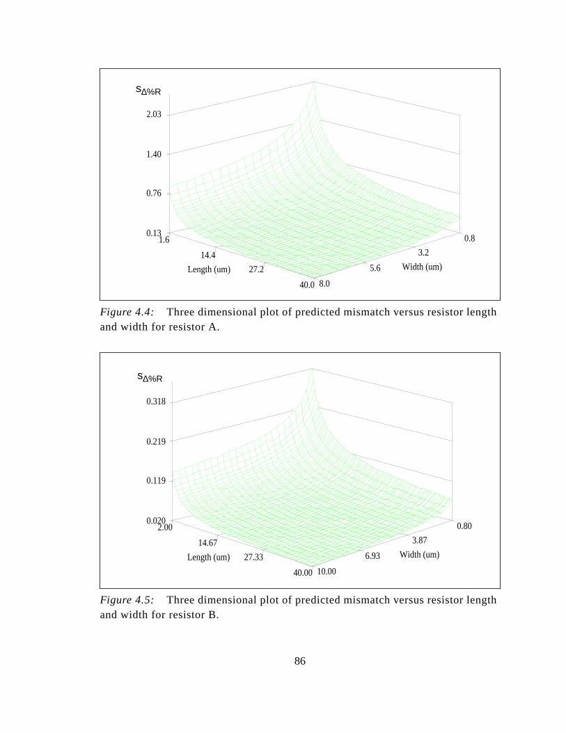
th
th
Figure 4.4: Three dimensional plot of predicted mismatch versus resistor lengand width for resistor A.
Figure 4.5: Three dimensional plot of predicted mismatch versus resistor lengand width for resistor B.
8.0
5.6
3.2
0.8
Width (um)
40.0
27.2
14.4
1.6
Length (um)
Stan Dev (MM)
0.13
0.76
1.40
2.03
s∆%R
10.00
6.93
3.87
0.80
Width (um)
40.00
27.33
14.67
2.00
Length (um)
Stan Dev (MM)
0.020
0.119
0.219
0.318
s∆%R
86

th
th
Figure 4.6: Three dimensional plot of predicted mismatch versus resistor lengand width for resistor C.
Figure 4.7: Three dimensional plot of predicted mismatch versus resistor lengand width for resistor D.
8.0
5.6
3.2
0.8
Width (um)
40.0
27.2
14.4
1.6
Length (um)
Stan Dev (MM)
0.14
1.06
1.99
2.92
s∆%R
10.00
6.93
3.87
0.80
Width (um)
40.00
27.33
14.67
2.00
Length (um)
Stan Dev (MM)
0.031
0.216
0.401
0.586
s∆%R
87
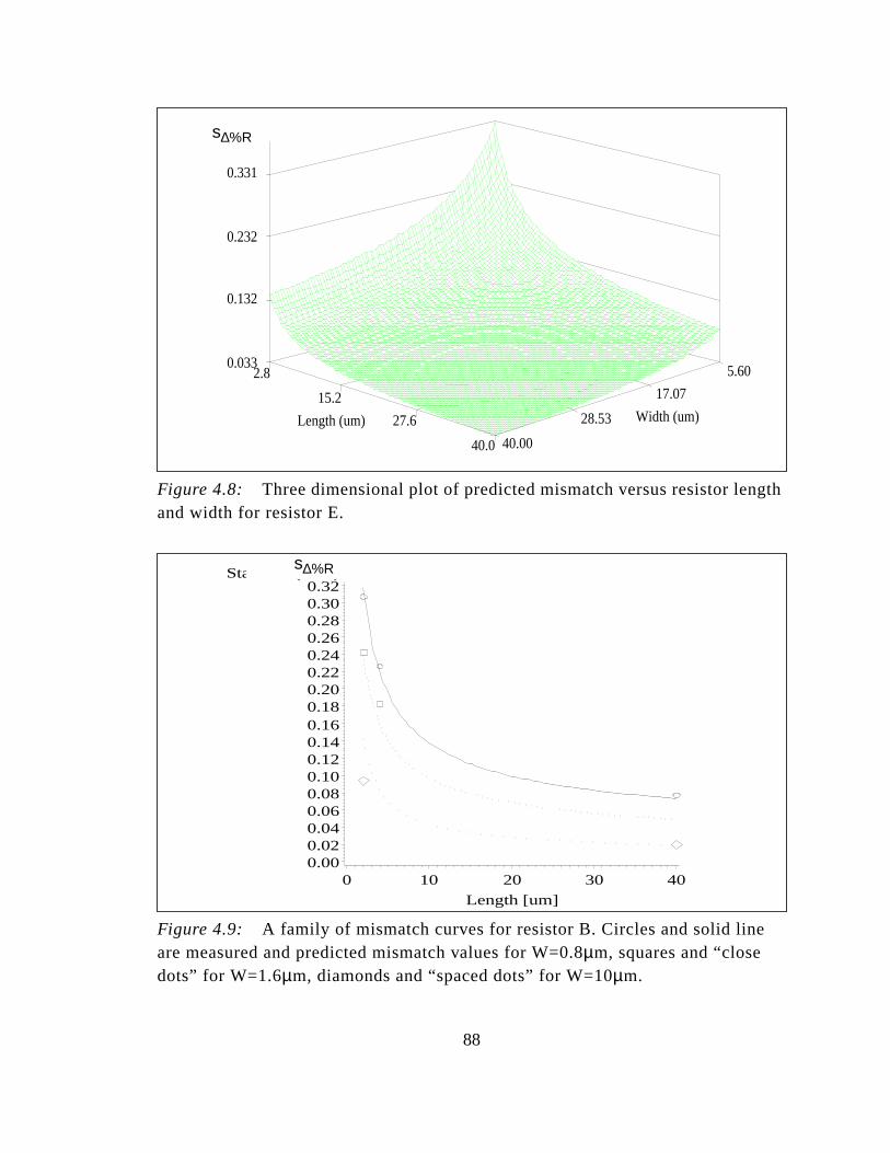
th
Figure 4.8: Three dimensional plot of predicted mismatch versus resistor lengand width for resistor E.Figure 4.9: A family of mismatch curves for resistor B. Circles and solid lineare measured and predicted mismatch values for W=0.8µm, squares and “closedots” for W=1.6µm, diamonds and “spaced dots” for W=10µm.
40.00
28.53
17.07
5.60
Width (um)
40.0
27.6
15.2
2.8
Length (um)
Stan Dev (MM)
0.033
0.132
0.232
0.331
s∆%R
Stan Dev(MM)
0.000.020.040.060.080.100.120.140.160.180.200.220.240.260.280.300.32
Length [um]
0 10 20 30 40
s∆%R
88
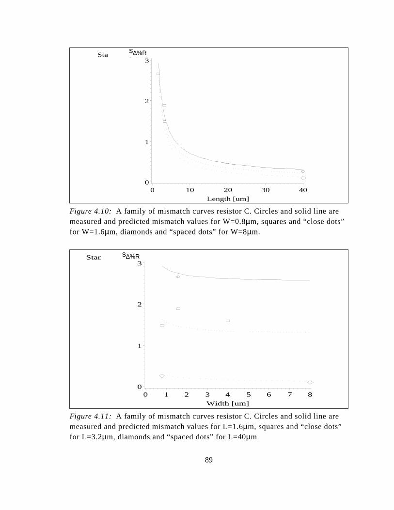
Figure 4.10: A family of mismatch curves resistor C. Circles and solid line aremeasured and predicted mismatch values for W=0.8µm, squares and “close dots”for W=1.6µm, diamonds and “spaced dots” for W=8µm.
Figure 4.11: A family of mismatch curves resistor C. Circles and solid line aremeasured and predicted mismatch values for L=1.6µm, squares and “close dots”for L=3.2µm, diamonds and “spaced dots” for L=40µm
Stan Dev(MM)
0
1
2
3
Length [um]
0 10 20 30 40
s∆%R
Stan Dev(MM)
0
1
2
3
Width [um]
0 1 2 3 4 5 6 7 8
s∆%R
89

seoint
seoint
Figure 4.12: A plot of the standard deviation of the mismatch versus the inversquare root of the resistor area for resistor B. The geometries for each data pare labeled as L[µm]/W[µm]. All devices have a minimum separation distance.
Figure 4.13: A plot of the standard deviation of the mismatch versus the inversquare root of the resistor area for resistor D. The geometries for each data pare labeled as L[µm]/W[µm]. All devices have a minimum separation distance.
Stan
Dev(MM)
0.000.020.040.060.080.100.120.140.160.180.200.220.240.260.280.300.32
1/sqrt(L*W) [um^-2]
0.0 0.1 0.2 0.3 0.4 0.5 0.6 0.7 0.8
W=min
L=min
L=W
s∆%R
2/0.8
4/0.8
2/1.6
4/1.6
2/1010/0.8
40/10
Stan
Dev(
MM)
0.0
0.1
0.2
0.3
0.4
0.5
0.6
0.7
0.8
1/sqrt(L*W) [um^-2]
0.0 0.1 0.2 0.3 0.4 0.5 0.6 0.7 0.8
L=W
L=min
W=min
s∆%R
2/0.8
4/0.8
2/1.6
4/1.6
2/10
10/0.840/10
90

the
tch
tch
er,
et
nt in
his
the
It is worth noting that the cut of L=W is not necessarily the minimum
attainable mismatch for a given area. That is, there may be a curve lower than
bottom curve in Figure 4.12 and Figure 4.13. Eq. (4.4) can be rewritten,
(4.7)
where A is the resistor area. For a constant area,
(4.8)
Setting Eq. (4.8) equal to zero and reducing, the condition for minimum misma
is
(4.9)
A comparison of the extracted mismatch model coefficients for all three
resistor is given in Table 4.3. In all three cases, the contributions to the misma
from the width variations is zero or near-zero. The length contribution, howev
increased dramatically for both the p-type and the n-type resistors as the she
resistance decreases. The substantially larger length variation is also appare
the asymmetric shape of the 3-dimensional plot in Figure 4.6 and Figure 4.7. T
increase is caused by a larger contribution from the contact resistance since
contact resistance is embedded in the parameter. As the sheet resistance
σR2
R2
------W
2σL2
A2
---------------σW
2
W2
--------σ2
LW
A--------------+ +=
W∂∂ σR
2
R2
------
A
2WσL2
A2
--------------- 2σW
2
W3
--------–=
LσL
σW--------W=
∆L
91

sis-
ve
rest-
E to
the
ease
r ana-
E
decreases, the contact resistance constitutes a larger portion of the overall re
tance for similar geometry resistors.
Table 4.3: A comparison of extracted resistor mismatch parameters for the firesistors.
The extracted area dependent terms, , in Table 4.3, yielded an inte
ing result. For the p-type resistors (C, D, and E), decreases from resistor
D but then increases D to C. Likewise, the increases from resistor B to A
which at first glance appears to counter the proposed Poisson distribution for
sheet resistance variation. That is, the sheet resistance variation should decr
as the number of implanted dopant atoms increases. This trend can be bette
lyzed by combining data from Table 4.1 and Table 4.3 into Table 4.4.
Parameter Resistor A Resistor B Resistor C Resistor D Resistor
(µm2)0.9735 0.05338 16.509 1.1507 0.03798
(µm2)0.0 6.298e-4 0.0 0.0 0.0
(µm2)4.8105 0.1389 2.665 0.0899 1.6389
(µm2)0.0 2.57e-8 0.0 2.144e-8 4.877e-8
(µm2)0.0 7.37e-8 1.567e-8 0.0 9.397e-7
Sheetresistance(ohms/sq)
51.3 732.6 89.6 876.14 4627.8
sL2
sW2
sLW2
dX2
dY2
sLW2
sLW2
sLW2
92

e
uni-
on-
forare
Table 4.4 contains the original parameters, the junction depths, th
peak dopant concentrations and the surface dopant concentrations. Since the
dopant profiles are unknown, the ion implant dose was estimated assuming a
form dopant profile with a dopant concentration equal to the surface dopant c
centration.
Table 4.4: A closer evaluation of the sheet resistance mismatch contributionsresistors A, B, and C. Note that resistors A and B are n-type while C, D, and Ep-type.
The sheet resistance for an n-type resistor is given by,
(4.10)
Parameter Resistor A Resistor B Resistor C Resistor D Resistor E
Junction Depth(µm)
0.325 0.6 0.425 0.85 2.2
Target surfacedopant conc.
(cm-3)
5.0e19 3.3e17 3.0e19 8.0e17 1.5e16
Target peakdopant conc.
(cm-3)
1.3e20 5.0e17 6.0e19 1.0e18 2.3e16
Estimated ionimplant dose
(cm-2)
1.625e15 1.98e13 1.275e15 6.8e13 3.3e12
4.8105 0.1389 2.665 0.0899 1.6389
sLW2
sLW2
ρs1
q n x( )µ x( ) xdsurface
X j
∫---------------------------------------------------- 1
q Nd x( )µ x( ) xdsurface
X j
∫--------------------------------------------------------≅ ≅
93

ty
n
ive
=
where is the electron carrier concentration at a depth, , is electron
mobility, is the junction depth, is the magnitude of the charge on an
electron, and is the n-type dopant concentration. Neglecting the mobili
dependence on the dopant concentration, if the dopant profile is uniform,
(4.11)
and the POV of Eq. (4.11) is,
. (4.12)
= , where is the ion implant dose, so,
(4.13)
Note that the square on and are missing since both variables were
assumed to be proportional to their variances through the Poisson distributio
assumption.
Using the estimates for , the junction depth, and the dose, from all f
resistor types in Table 4.4, estimates for and , = 4.25e12 and
n x( ) x µ x( )
X j q
Nd x( )
ρs1
qµNdX j---------------------≅
σρs
2
ρs2
--------σNd
2
Nd---------
σXj
2
X j2
---------+=
σNd
2
Nd---------
σDII
2
DII---------- DII
σρs
2
ρs2
--------σLW
2
LW-----------
σDII
2
DII----------
σXj
2
X j2
---------+= =
Nd DII
sLW2
σDII
2 σXj
2sDII
2sX j
2
94
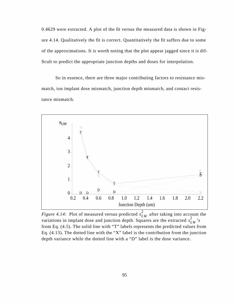
Fig-
me
dif-
mis-
is-
he’smn
0.4629 were extracted. A plot of the fit versus the measured data is shown in
ure 4.14. Qualitatively the fit is correct. Quantitatively the fit suffers due to so
of the approximations. It is worth noting that the plot appear jagged since it is
ficult to predict the appropriate junction depths and doses for interpolation.
So in essence, there are three major contributing factors to resistance
match, ion implant dose mismatch, junction depth mismatch, and contact res
tance mismatch.
Figure 4.14: Plot of measured versus predicted after taking into account tvariations in implant dose and junction depth. Squares are the extractedfrom Eq. (4.5). The solid line with “T” labels represents the predicted values froEq. (4.13). The dotted line with the “X” label is the contribution from the junctiodepth variance while the dotted line with a “D” label is the dose variance.
Variance(sL^2)
0
1
2
3
4
5
Junction Depth (um)0.2 0.4 0.6 0.8 1.0 1.2 1.4 1.6 1.8 2.0 2.2
T
T
T
T
T
D
DDDD
sLW
sLW2
sLW2
95

lly
ffer-
he
st
e. In
4.5 Mismatch of dissimilar geometries
The classical mismatch test structure consists of a simple pair of identica
drawn devices. The mismatch statistic is either the percent difference or the di
ence between the two devices in the pair, depending on the application. For t
moment, only the percent difference will be discussed.
The percent difference is calculated in either one of two ways. In the fir
case,
(4.14)
where, is the resistor mismatch statistic and R1 and R2 are the two
resistances. In the second case,
. (4.15)
Both cases can be summarized as
(4.16)
where is the expected value of the resistance and R is the measured valu
Eq. (4.14), it is assumed that R2 is the “true” value of the resistance and the
mismatch is gathered by accounting for the extent in which R1 deviates from the
“true” value. Similarly, Eq. (4.15) considers the mismatch to be the deviation
∆%R 100R1 R2–( )
R2-----------------------=
∆%R
∆%R 200R1 R2–( )R1 R+
2
-----------------------=
∆%R 100R E R( )–( )
E R( )---------------------------=
E R( )
96

atch
as an
f the
?
such
of
about a resistance that is half-way between R1 and R2. As a matter of practice, Eq.
(4.14) and Eq. (4.15) are numerically equivalent since the extent of the mism
is much smaller than the expected value. One degree of freedom is consumed
estimate of the expectation value and the second is used for the calculation o
deviation about the expected value.
Although Eq. (4.14) assumes R2 to be the “true” value of the resistor, in
reality both R1 and R2 deviate from the expected value. If R1 and R2 are identi-
cally drawn,
. (4.17)
But what happens to Eq. (4.17) when R1 and R2 are not identically drawn (i.e. R2
is twice as long as R1)? How is the total variance split between the two devices
Conceptually one should be able to establish a situation in which R1 is compared
to many other resistors, and those resistors in turn, compared to each other,
that the fractional separation of the variances in each possible pairwise
combination can be simultaneously solved.
The mismatch of dissimilar devices is based upon taking the simple ratio
the two resistances, namely
(4.18)
σR1
2 σR2
2σ∆%R
2
2-------------= =
∆%R 100R1 R2–( )
R2----------------------- 100
R1
R2------ 1–
= =
97
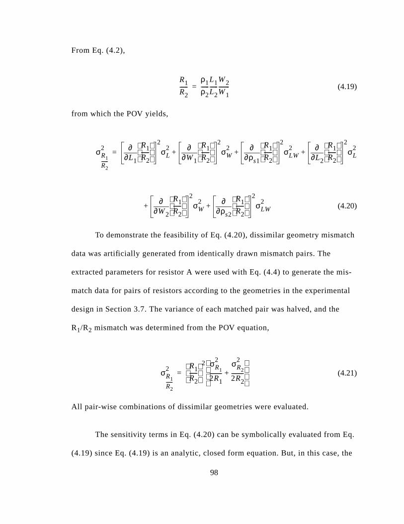
ch
mis-
ntal
e
q.
the
From Eq. (4.2),
(4.19)
from which the POV yields,
(4.20)
To demonstrate the feasibility of Eq. (4.20), dissimilar geometry mismat
data was artificially generated from identically drawn mismatch pairs. The
extracted parameters for resistor A were used with Eq. (4.4) to generate the
match data for pairs of resistors according to the geometries in the experime
design in Section 3.7. The variance of each matched pair was halved, and th
R1/R2 mismatch was determined from the POV equation,
(4.21)
All pair-wise combinations of dissimilar geometries were evaluated.
The sensitivity terms in Eq. (4.20) can be symbolically evaluated from E
(4.19) since Eq. (4.19) is an analytic, closed form equation. But, in this case,
R1
R2------
ρ1
ρ2------
L1
L2------
W2
W1--------=
σR1
R2------
2
L1∂∂ R1
R2------
2
σL2
W1∂∂ R1
R2------
2
σW2
ρs1∂∂ R1
R2------
2
σLW2
L2∂∂ R1
R2------
2
σL2
+ + +=
W2∂∂ R1
R2------
2
σW2
ρs2∂∂ R1
R2------
2
σLW2
+ +
σR1
R2------
2 R1
R2------
2 σR1
2
2R1---------
σR2
2
2R2---------+
=
98

om-
error,
ti-
half
e-
sensitivities were evaluated numerically to broaden the generality of this
approach.
From the analysis of variance for the fit of the dissimilar geometries in
Table 4.5, it is apparent that the regression for dissimilar geometries works. C
paring the relative values of the mean square regression and the mean square
the mean square error can be attributed to round-off error. The parameter es
mates are given in Table 4.6. The estimates for and are approximately
of the estimates for resistor A in Table 4.3. The slight offset in all three param
ters can be attributed to the round-off error.
Table 4.5: ANOVA for the dissimilar geometry analysis based on resistor A.
Source DFSum ofSquares
MeanSquare
Regression 3 3.8680e13 1.2893e13
Residual 39 8964.57 229.8607
Uncorrected Total 42 3.8680e13
(Corrected Total) 41 3.7712e13
sLW2
sL2
99
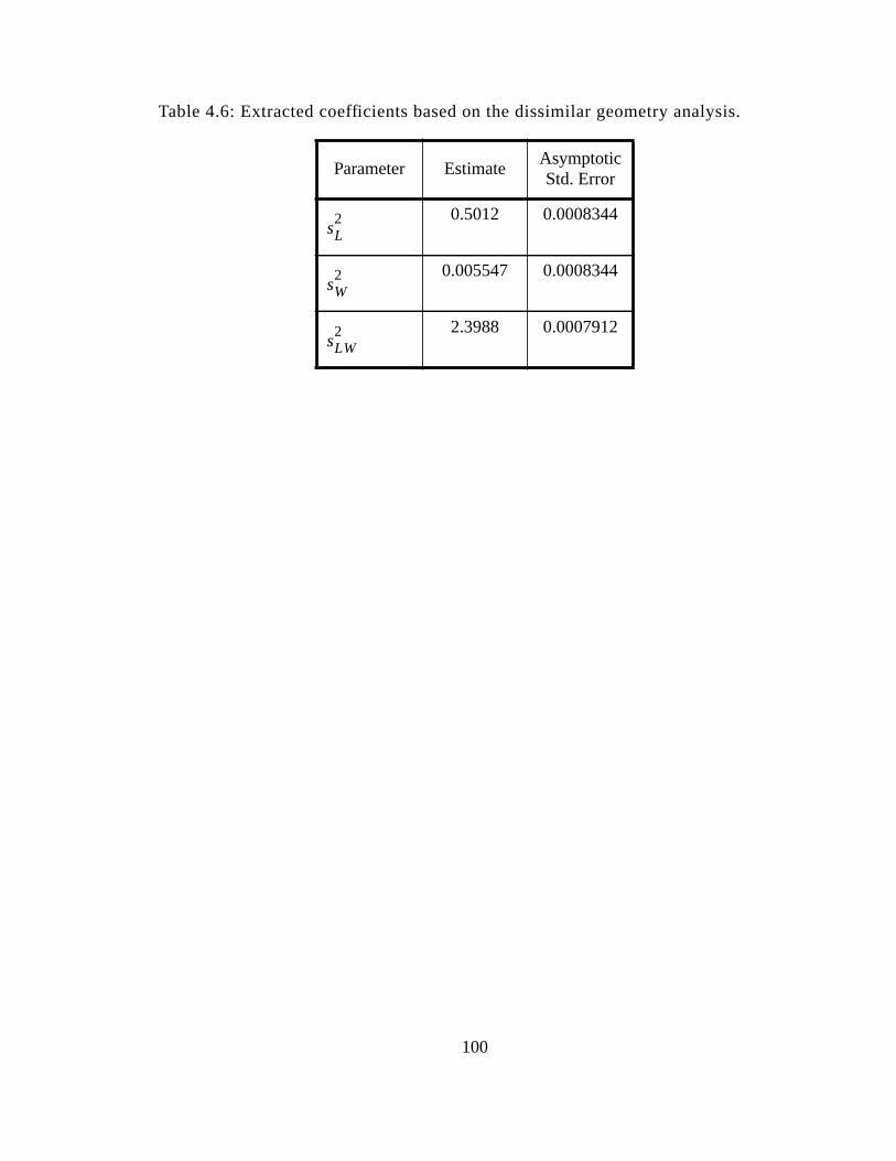
Table 4.6: Extracted coefficients based on the dissimilar geometry analysis.
Parameter EstimateAsymptoticStd. Error
0.5012 0.0008344
0.005547 0.0008344
2.3988 0.0007912
sL2
sW2
sLW2
100

ent
from
dis-
ges
a
in-
e
ort
e in
ence
o-
Chapter 5 MOSFET Mismatch
5.1 Prior work
Much of the existing mismatch theory has been derived from MOSFET
matching as discussed in Section 3.6. Additional, empirical, principal compon
approaches were developed by Inohira et al. [28] and in a number of papers
Ohio State University [29, 30, 27, 31, 32, 33, 34, 23, 21, 21]. This approach is
cussed at greater length in Section 3.4.
Gregor [35] demonstrated the impact of neighboring topographical chan
on the Id mismatch of a MOSFET pair. A vertical step in topography that is in
close proximity to one of the two devices in a MOS matched pair can produce
slightly thinner photoresist layer for the polysilicon gate patterning step. The th
ner resist will produce a slightly wider polysilicon gate which in turn will produc
a mismatch offset.
Steyaert et al. [36] made modifications to the Pelgrom model [2] by
attempting to account for the MOSFET effective length and width, and the sh
channel and narrow channel effects (see [37]). Instead of modeling the varianc
the Vt mismatch as a 1/(drawn area) dependence, a 1/(effective area) depend
was used. The short channel effect and the narrow width effect were accomm
dated by using the model,
101
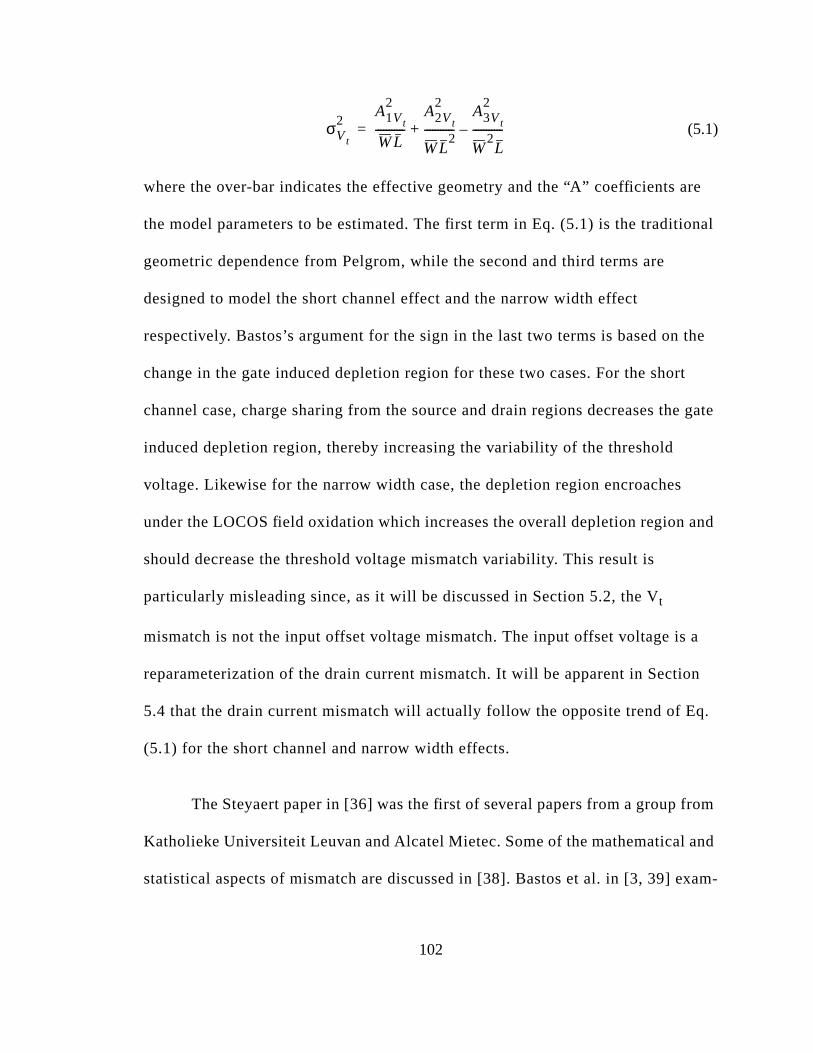
re
nal
the
rt
e gate
nd
a
n
q.
om
nd
am-
(5.1)
where the over-bar indicates the effective geometry and the “A” coefficients a
the model parameters to be estimated. The first term in Eq. (5.1) is the traditio
geometric dependence from Pelgrom, while the second and third terms are
designed to model the short channel effect and the narrow width effect
respectively. Bastos’s argument for the sign in the last two terms is based on
change in the gate induced depletion region for these two cases. For the sho
channel case, charge sharing from the source and drain regions decreases th
induced depletion region, thereby increasing the variability of the threshold
voltage. Likewise for the narrow width case, the depletion region encroaches
under the LOCOS field oxidation which increases the overall depletion region a
should decrease the threshold voltage mismatch variability. This result is
particularly misleading since, as it will be discussed in Section 5.2, the Vt
mismatch is not the input offset voltage mismatch. The input offset voltage is
reparameterization of the drain current mismatch. It will be apparent in Sectio
5.4 that the drain current mismatch will actually follow the opposite trend of E
(5.1) for the short channel and narrow width effects.
The Steyaert paper in [36] was the first of several papers from a group fr
Katholieke Universiteit Leuvan and Alcatel Mietec. Some of the mathematical a
statistical aspects of mismatch are discussed in [38]. Bastos et al. in [3, 39] ex
σVt
2A1Vt
2
W L-----------
A2Vt
2
W L2
-----------A3Vt
2
W2L
-----------–+=
102

old
d
e
to
ea-
[40]
OS-
troi-
l. in
fer-
ctic
pro-
ver
t
r-
e
e
ined four different extraction approaches for extracting the mismatch in thresh
voltage, the gain factor, , and the body effect, . It was determine
that the body effect did not contributed to the drain current mismatch for thes
measurements. Also, it was found that the preferred method for extraction is
measure the drain current mismatch and extract the Vt and mismatch through a
simple POV equation. This result is consistent with the observations in this tr
tise, but this work presents a more comprehensive approach. Bastos et al., in
performed some experiments on different layout styles. In general, fingered M
FETs led to the poorest mismatch, but inter-digitated fingers and common cen
ded cross coupled scheme showed excellent results as expected. Bastos et a
[16, 17] placed an array of MOSFET test structures into package using two dif
ent bonding schemes, eutectic solder and polyimide. It was found that the eute
bond led to larger stress gradients which can be up to 10 times greater than
cess gradients.
A qualitative but comprehensive discussion of the mismatch behavior o
the geometry and bias space is given by Forti and Wright [41] for four differen
processes. Measuring Id mismatch for MOSFETs in the weak and moderate inve
sion region (overdrive < 1.5V), trends over geometry were inconsistent with th
work in [2, 6, 7, 8] were observed. In addition, it was found that increasing th
bulk bias tended to increase the Id mismatch.
β µCoxWL-----= γ
β
103

the
in
ng
ent
is-
and
e
m
ales
the
volt-
tain
the
wise
In addition to ion implant striations discussed inSection 3.1.3, Pavasovic et
al. [14] presented mismatch data for the subthreshold region. It was found that
perimeter devices of a 32x32 array of MOSFETs tended to experience a shift
the drain current which gives further evidence of the possible benefits of addi
dummy devices to a matched pair.
Serrano-Gotarredona and Linares-Barranco [42, 43]built an addressible array
of MOSFETs to gather mismatch data on many structures without the requirem
of stepping across multiple pad arrays and the availability of switch matrix. M
match data was gathered for the threshold voltage, gain factor, and body effect
was fitted with the Pelgrom model. Data in this report clearly show some of th
shortcomings of the Pelgrom model.
Wong et al. [44, 45] attempted to explain the deviations from the Pelgro
model by adjusting the power, stating that the mismatch standard deviation sc
with 1/(gate area)0.75.
Like the approaches by Bastos [3, 16, 17, 40, 39], Lovett [46, 47] used
effective geometries, rather than the drawn geometries to scale the threshold
age and the gain factor mismatch. With this consideration, not all devices main
an equivalent mismatch for the same gate area. Lovett derived a solution for
optimum length, and width for mismatch given an area constraint. This result
seems academic at best, since the width/length ratio is often determined other
(e.g. to set the transconductance).
104

to
n a
is-
on
etry
Phil-
pled
uce
the
Karhunen et al. [48] presented an analysis of the sensitivity of mismatch
various common centroided schemes.
Portmann et al. [49] presented another addressible array of MOSFETs o
SOI CMOS process. Mismatch data collected for threshold and gain factor m
match was not particularly noteworthy.
Ohzone et al. [50, 51] explored the effect of source/drain ion implantati
angle on mismatch and ring oscillator performance. As expected, the asymm
in the source and drain implant caused by shadowing from the MOSFET gate
induced asymmetries in the mismatch.
By far, the Pelgrom model [2] (with a later review in [52]), developed at
Philips, is the primary reference point for most of the subsequent mismatch
research despite it having the weakest physical basis. The publications from
ips continued with work from Tuinhout and Elzinga. Elzinga [13] described in
greater detail the impact of the gradient effects and the benefits of cross-cou
layouts. Tuinhout et al. [10] examined the effects of metal overlay over a MOS
matched pair. It was found that placing metal layers over MOSFETs can prod
parametric shifts which are catastrophic to MOS matched pairs, particularly if
metal overlay is asymmetric. Placing metal interconnects over MOSFETs is a
fairly common design practice. In [10], the parametric shifts were attributed to
dangling bonds in the Si / SiO2 interface under the gate, which could be signifi-
cantly improved with an added forming gas (N2/H2) anneal. It was subsequently
105
f the
on
on
n
te
n
e an
ed
ffer-
e is
rt
s
es
determined in [12] from test structures placed at a 45 degree angle that part o
parametric shift was induced by localized stress from the metal layers. As
expected, metal 1 created larger shifts than subsequent metal layers.
Tuinhout et al. [53] also evaluated the effects of polysilicon gate doping
MOSFET mismatch. The polysilicon dopant rapid thermal anneal (RTA) cycle
played a major contributing factor to threshold voltage mismatch through the
trade-off of two competing mechanisms. For an inadequate polysilicon dopant
anneal, the polysilicon dopant doesn’t completely diffuse through the polysilic
gate, leading to polysilicon depletion effects. For excessive polysilicon diffusio
times, the boron in the polysilicon gate is liable to diffuse right through the ga
oxide, causing localized shift in the threshold voltage.
Elzinga [54] demonstrated the importance the silicon surface preparatio
before salicidation of the polysilicon gate and source drain regions which can b
added source of mismatch variation through the partial anneal of the dangling
bonds under the gate.
Bolt et al. [55], also from Philips, performed an experiment on self-align
gates compared to a non-self-aligned gate and found there to be virtually no di
ence in the results. Upon closer examination of their data, it appears that ther
no increase in the drain current mismatch for large gate biases on a wide sho
device. As will be discussed in Section 5.4, this geometry and bias condition i
most sensitive to series resistances. It would appear that neither of their devic
106

eir
ar to
es.
for
tch.
om
ass
eak-
the
in
in
, 53,
t in
en-
were susceptible to source/drain resistance mismatch which would explain th
observation. In addition, these authors provide plots of nMOS and pMOS Vt and
gain factor mismatch versus 1/(gate area). The threshold voltage curves appe
be well behaved with a significant deviation from the model for large area devic
The gain factor mismatch shows significant scatter about the 1/(gate area) line
the various gate areas, which indicates a perimeter contribution to the misma
Jaeger et al. [15] discussed the shifts in MOSFET mismatch produced fr
packaging stresses which are caused by piezo-resistive shifts in the effective m
of the carriers. Parametric shifts of up to 5-10% can be observed. Generally sp
ing, on a [100] wafer, a pMOS device placed in the <100> direction (+/- 45
degrees rotation) will experience a minimum parametric shift, followed by a
nMOS device in the <110> direction (0 or 90 degrees rotation and a pMOS in
<110> direction. The worst piezo resistive effect is observed for a nMOS device
the <100> direction.
5.2 Method
The primary underlying assumption for the MOSFET mismatch models
[1, 4, 56, 2, 3, 9, 13, 16, 17, 40, 39, 11, 12, 10, 36, 38, 57, 58, 44, 46, 45, 59
60, 61, 54, 47, 62, 52] is that the input offset voltage for a MOS pair is the Vt mis-
match for MOSFETs with separated gates. The input offset voltage is the offse
gate voltage to create identical drain currents in two matched MOSFETs. Ess
tially, the input offset voltage mismatch is same as the Id mismatch. It is important
107

lt-
n
,
l.
ess,
he
,
.
ve
.
to recall that Vt is just one of several possible contributors to the input offset vo
age. The Vt is a conceptual artifact, and is not a physical process parameter. I
fact, Vt is an electrical parameter. The mismatch in Vt is based on several process
parameters as pointed out in [6, 7, 8]. Using the simple Ids relationship in the lin-
ear region, the input offset voltage, , is,
. (5.2)
The first quantity in paranthesis in Eq. (5.2) is the threshold voltage mismatch
which is clearly not the only contributer to the mismatch.
Like the resistor, BPV was used to derive the MOSFET mismatch mode
Eight process parameters were considered. They were, the gate oxide thickn
, the field oxide encroachment / width bias, , the flat band voltage, , t
substrate dopant concentration, , the mobility, , polysilicon gate length
, short channel change in threshold, and the series sheet resistance,
The tilde (~) above the variable is equivalent to notation but is used to sa
space..
The statistical model is based upon Motorola’s proprietary SSIM model
Other MOSFET models such as BSIM3v3 [63] are also well suited for this
Vios
Vios Vgs1 Vgs2–
Vt1 Vt2–( )Vds1 Vds2–( )
2---------------------------------- I d
L1
Vds1µ1Cox1W1---------------------------------------
L2
Vds2µ2Cox2W2---------------------------------------–
+ +
=
=
Vios
tox ∆W V fb
Nsub µo
∆L Vtl ρsh
∆%
108

a
xide
b-
ge.
e gate
te
nce
aproach. The SSIM model, like most other SPICE MOSFET models, contains
redundant parameterization of the substrate dopant concentration and gate o
thickness through the threshold voltage. Separate parameters exist for the su
strate dopant concentration, the gate oxide thickness, and the threshold volta
The threshold voltage depends on the substrate dopant concentration and th
oxide thickness,
(5.3)
where is the flat band voltage, is Boltzmann’s constant, is the
temperature, is magnitude of the charge on an electron, is the substra
dopant concentration, and is the intrinsic carrier concentration. The differe
in threshold voltage produced from an offset in the process parameters, ,
, and from Eq. (5.3) is,
Vt V fb 2kTq
------Nsub
ni------------
ln
2tox NsubεSiεOkTNsub
ni------------
ln
εoxεO------------------------------------------------------------------------+ +=
V fb k T
q Nsub
ni
V fb
Nsub tox
109
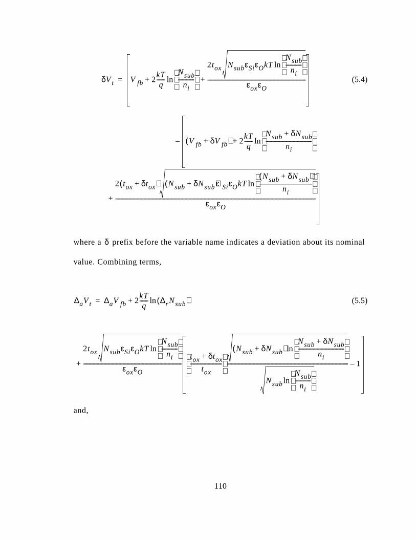
inal
(5.4)
where a prefix before the variable name indicates a deviation about its nom
value. Combining terms,
(5.5)
and,
δVt V fb 2kTq
------Nsub
ni------------
ln
2tox NsubεSiεOkTNsub
ni------------
ln
εoxεO------------------------------------------------------------------------+ +
V fb δV fb+( ) 2kTq
------Nsub δNsub+
ni----------------------------------
ln
2 tox δtox+( ) Nsub δNsub+( )εSiεOkTNsub δNsub+( )
ni---------------------------------------
ln
εoxεO---------------------------------------------------------------------------------------------------------------------------------------------------
+
+
–
=
δ
∆aVt ∆aV fb 2kTq
------ ∆r Nsub( )ln
2tox NsubεSiεOkTNsub
ni------------
ln
εoxεO------------------------------------------------------------------------
tox δtox+
tox-----------------------
Nsub δNsub+( )Nsub δNsub+
ni----------------------------------
ln
Nsub
Nsub
ni------------
ln
----------------------------------------------------------------------------------------- 1–
+
+
=
110
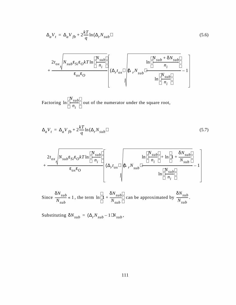
(5.6)
Factoring out of the numerator under the square root,
(5.7)
Since , the term can be approximated by .
Substituting ,
∆aVt ∆aV fb 2kTq
------ ∆r Nsub( )ln
2tox NsubεSiεOkTNsub
ni------------
ln
εoxεO------------------------------------------------------------------------ ∆r tox( ) ∆r N
sub( )
Nsub δNsub+
ni----------------------------------
ln
Nsub
ni------------
ln
--------------------------------------------- 1–
+
+
=
Nsub
ni------------
ln
∆aVt ∆aV fb 2kTq
------ ∆r Nsub( )ln
2tox NsubεSiεOkTNsub
ni------------
ln
εoxεO------------------------------------------------------------------------ ∆r tox( ) ∆r N
sub( )
Nsub
ni------------
ln 1δNsub
Nsub---------------+
ln+
Nsub
ni------------
ln
------------------------------------------------------------------ 1–
+
+
=
δNsub
Nsub--------------- 1« 1
δNsub
Nsub---------------+
lnδNsub
Nsub---------------
δNsub ∆r Nsub 1–( )Nsub=
111
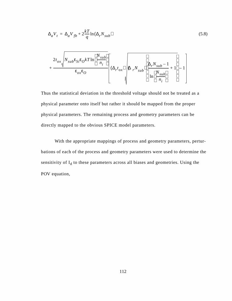
a
rtur-
e the
e
(5.8)
Thus the statistical deviation in the threshold voltage should not be treated as
physical parameter onto itself but rather it should be mapped from the proper
physical parameters. The remaining process and geometry parameters can be
directly mapped to the obvious SPICE model parameters.
With the appropriate mappings of process and geometry parameters, pe
bations of each of the process and geometry parameters were used to determin
sensitivity of Id to these parameters across all biases and geometries. Using th
POV equation,
∆aVt ∆aV fb 2kTq
------ ∆r Nsub( )ln
2tox NsubεSiεOkTNsub
ni------------
ln
εoxεO------------------------------------------------------------------------ ∆r tox( ) ∆r N
sub( )
∆r Nsub 1–
Nsub
ni------------
ln
--------------------------- 1+
1–
+
+
=
112

the
ast
ce
the
W
x
fb
o
L
tl
h
ub
(5.9)
Given a vector of Id mismatch values, over many biases and geometries, the
mismatch variances in the fundamental process and geometry parameters on
right side of Eq. (5.9) can be extracted by way of linear regression or other le
squares solvers. This method is refered to as the Back Propagation of Varian
(BPV) per [19].
The proposed model has the following advantages:
• It gives estimates for the variations of the physical parameters causing
mismatch.
• It automatically accounts for the effective length and width.
σI d12
σI d22
σI d32
…
σI dn2
∆Wd
dId1
2
toxd
dId1
2
V fbd
dId1
2
µod
dId1
2
∆Ld
dId1
2
Vtld
dId1
2
ρshd
dId1
2
Nsubd
dId1
2
∆Wd
dId2
2
toxd
dId2
2
V fbd
dId2
2
µod
dId2
2
∆Ld
dId2
2
Vtld
dId2
2
ρshd
dId1
2
Nsubd
dId1
2
∆Wd
dId3
2
toxd
dId3
2
V fbd
dId3
2
µod
dId3
2
∆Ld
dId3
2
Vtld
dId3
2
ρshd
dId1
2
Nsubd
dId1
2
… … … … … … … …
∆Wd
dIdn
2
toxd
dIdn
2
V fbd
dIdn
2
µod
dIdn
2
∆Ld
dIdn
2
Vtld
dIdn
2
ρshd
dIdn
2
Nsubd
dIdn
2
σ∆2
σ to
2
σV2
σµ2
σ∆2
σV2
σρs
2
σNs
2
=
113

rt
s.
lin-
con-
DD
ble
er
e
• It automatically accounts for the short channel effect, the reverse sho
channel effect, the narrow width effect, and the inverse narrow width
effect.
• It automatically accommodates the source and drain series resistance
• It is continuous over bias region. There is not a separate model for the
ear and saturation regions.
• It is easy to implement.
5.3 A 0.8µm Power BiCMOS Technology
5.3.1 Process conditions and measurements
Mismatch in low voltage nMOS and pMOS devices from a 0.8µm power
BiCMOS technology were characterized using Eq. (5.9). These devices each
tain a self aligned polysilicon gate with a 20nm gate oxide, but do not have a L
layer or a punchthrough implant. The minimum polysilicon gate length to 1.6µm
which is twice the minimum geometry.
Geometries were placed on a characterization test mask as listed in Ta
5.1. The “X direction” in Table 5.1 is the direction parallel to the side of the waf
with the notch. The “Y direction” is orthogonal to the X. All mismatch pairs wer
laid out in a common source configuration and the gate pads were combined.
114
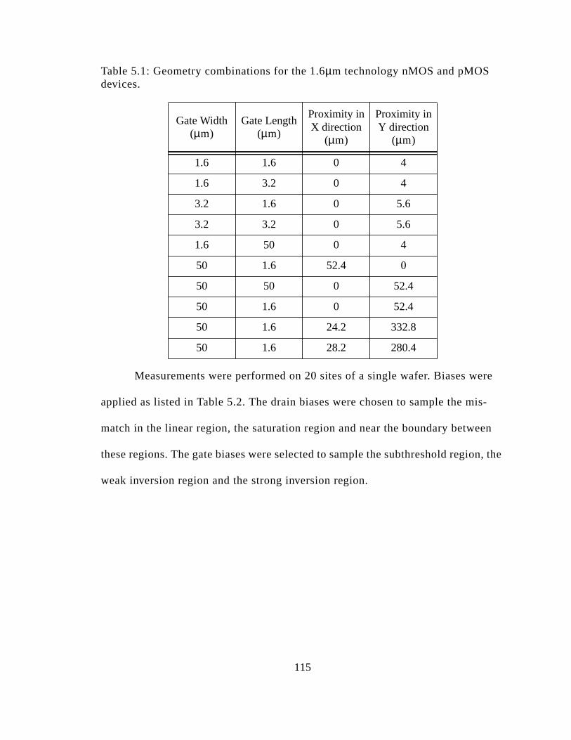
re
is-
en
n, the
Table 5.1: Geometry combinations for the 1.6µm technology nMOS and pMOSdevices.
Measurements were performed on 20 sites of a single wafer. Biases we
applied as listed in Table 5.2. The drain biases were chosen to sample the m
match in the linear region, the saturation region and near the boundary betwe
these regions. The gate biases were selected to sample the subthreshold regio
weak inversion region and the strong inversion region.
Gate Width(µm)
Gate Length(µm)
Proximity inX direction
(µm)
Proximity inY direction
(µm)
1.6 1.6 0 4
1.6 3.2 0 4
3.2 1.6 0 5.6
3.2 3.2 0 5.6
1.6 50 0 4
50 1.6 52.4 0
50 50 0 52.4
50 1.6 0 52.4
50 1.6 24.2 332.8
50 1.6 28.2 280.4
115
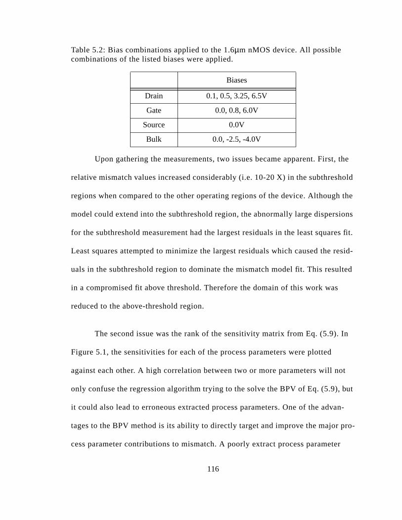
, the
hold
the
ions
es fit.
resid-
lted
In
ot
but
an-
ro-
r
Table 5.2: Bias combinations applied to the 1.6µm nMOS device. All possiblecombinations of the listed biases were applied.
Upon gathering the measurements, two issues became apparent. First
relative mismatch values increased considerably (i.e. 10-20 X) in the subthres
regions when compared to the other operating regions of the device. Although
model could extend into the subthreshold region, the abnormally large dispers
for the subthreshold measurement had the largest residuals in the least squar
Least squares attempted to minimize the largest residuals which caused the
uals in the subthreshold region to dominate the mismatch model fit. This resu
in a compromised fit above threshold. Therefore the domain of this work was
reduced to the above-threshold region.
The second issue was the rank of the sensitivity matrix from Eq. (5.9).
Figure 5.1, the sensitivities for each of the process parameters were plotted
against each other. A high correlation between two or more parameters will n
only confuse the regression algorithm trying to the solve the BPV of Eq. (5.9),
it could also lead to erroneous extracted process parameters. One of the adv
tages to the BPV method is its ability to directly target and improve the major p
cess parameter contributions to mismatch. A poorly extract process paramete
Biases
Drain 0.1, 0.5, 3.25, 6.5V
Gate 0.0, 0.8, 6.0V
Source 0.0V
Bulk 0.0, -2.5, -4.0V
116

here
lation
bove
ame
age
ved.
could cause the device engineers to work on the wrong part of the process. T
appears to be a reasonable separation of the parameters except for the corre
between and in Figure 5.1.
The bias conditions on the gate were changed to guarantee operation a
the threshold. Part of the difficulty in defining the bias conditions for the gate
voltage is that the threshold voltage changes over the bulk bias range. At the s
time, it is desirable to gain mismatch data in the moderate inversion region.
The measurement algorithm was rewritten to dynamically set the gate
biases at specified levels in Table 5.3. The algorithm first sweeps the gate volt
and calculates the gate voltage at which the peak transconductance is obser
The gate voltages are then set to (Vg at peak gm), the max Vg, and half-way
between those two values.
Table 5.3: Bias combinations applied to the 1.6µm nMOS device. All possiblecombinations of the listed biases were applied.
Biases
Drain 0.1, 0.5, 3.25, 6.5V
Gate (Vg @ peak gm),[(V g @ peak gm) + max(Vg)]/2,
max(Vg)
Source 0.0V
Bulk 0.0, -2.5, -4.0V
tox Nsub
117

lcu-
atter
cat-
Upon application of these biases the sensitivities in Figure 5.2 were ca
lated. There is a significant improvement in the scatter of these plots. The sc
in versus improved only marginally but there appears to be enough s
ter to avoid singularity in the sensitivity matrix.
tox Nsub
118
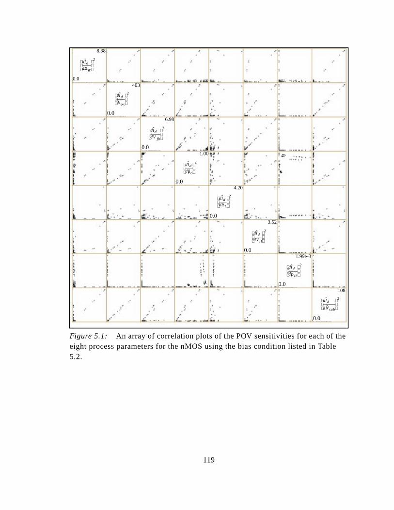
ele
.
Figure 5.1: An array of correlation plots of the POV sensitivities for each of theight process parameters for the nMOS using the bias condition listed in Tab5.2.
∆Wd
dId
2
toxd
dId
2
V fbd
dId
2
µod
dId
2
∆Ld
dId
2
Vtld
dId
2
ρshd
dId
2
Nsubd
dId
2
8.38
0.0
0.0
0.0
0.0
0.0
0.0
0.0
0.0
403
6.98
1.00
4.20
3.52
1.99e-3
108
119
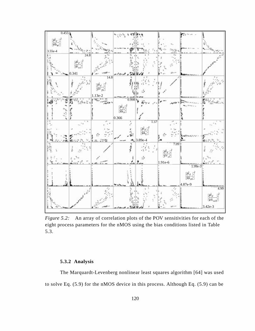
eble
sed
be
.
Figure 5.2: An array of correlation plots of the POV sensitivities for each of theight process parameters for the nMOS using the bias conditions listed in Ta5.3.
5.3.2 Analysis
The Marquardt-Levenberg nonlinear least squares algorithm [64] was u
to solve Eq. (5.9) for the nMOS device in this process. Although Eq. (5.9) can
∆Wd
dId
2
toxd
dId
2
V fbd
dId
2
µod
dId
2
∆Ld
dId
2
Vtld
dId
2
ρshd
dId
2
Nsubd
dId
2
0.455
3.55e-4
0.341
1.13e-2
0.366
3.89e-4
1.91e-6
4.87e-9
3.42e-3
24.8
14.8
0.998
1.57
7.09
1.99e-3
4.99
120

n to
ative
a
ence
-
r
e of
ic in
rrors
terest.
solved analytically through linear regression, non-linear regression was chose
allow boundary conditions on the process parameters variances to avoid neg
values. Negative values result from situations in which the “true” variance for
given process parameter is zero or near zero. In this case, the estimated confid
interval can contain negative values, which is an artifact of the statistical sam
pling. An alternative approach to placing boundary conditions on the nonlinea
solution, is to use linear regression and re-assign the negative values to a valu
zero.
Table 5.4 shows the resultant analysis of variance(ANOVA) for the fit.
Table 5.5 shows the extracted parameters. The standard errors are asymptot
Table 5.5 since nonlinear regression was used. The relatively large standard e
are not a concern since the process parameter estimates were the primary in
Table 5.4: 0.16µm technology nMOS ANOVA.
Source DFSum ofSquares
MeanSquare
Regression 8 9316.7070 1164.5884
Residual 319 504.3887 1.5812
Uncorrected Total 327 9821.09579
(Corrected Total) 326 8512.2509
121
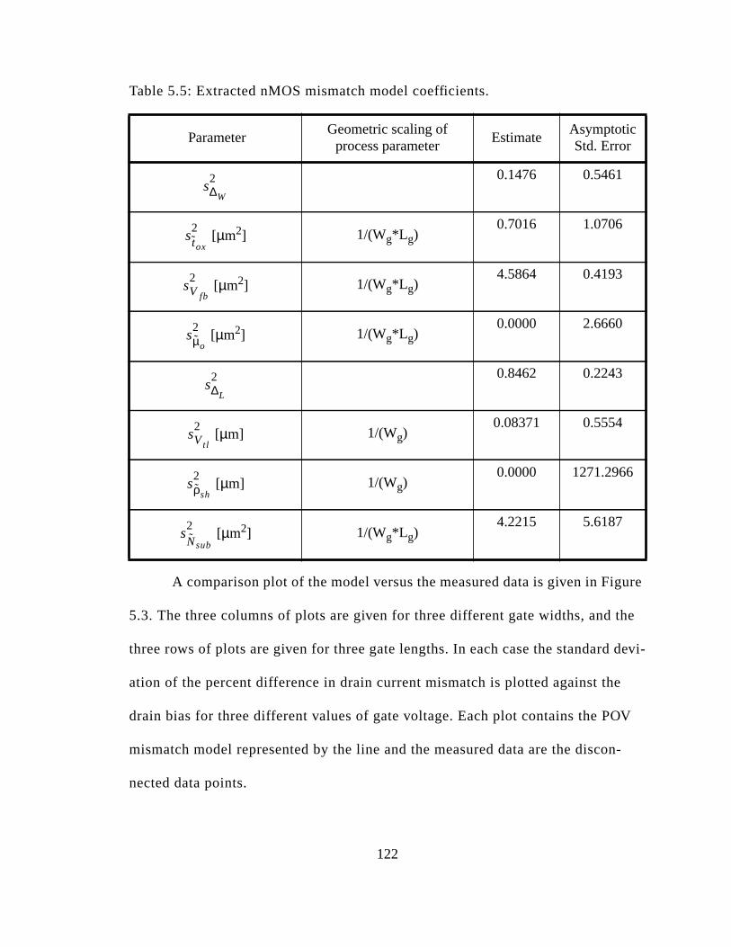
ure
the
devi-
e
V
n-
Table 5.5: Extracted nMOS mismatch model coefficients.
A comparison plot of the model versus the measured data is given in Fig
5.3. The three columns of plots are given for three different gate widths, and
three rows of plots are given for three gate lengths. In each case the standard
ation of the percent difference in drain current mismatch is plotted against th
drain bias for three different values of gate voltage. Each plot contains the PO
mismatch model represented by the line and the measured data are the disco
nected data points.
ParameterGeometric scaling of
process parameterEstimate
AsymptoticStd. Error
0.1476 0.5461
[µm2] 1/(Wg*L g)0.7016 1.0706
[µm2] 1/(Wg*L g)4.5864 0.4193
[µm2] 1/(Wg*L g)0.0000 2.6660
0.8462 0.2243
[µm] 1/(Wg)0.08371 0.5554
[µm] 1/(Wg)0.0000 1271.2966
[µm2] 1/(Wg*L g)4.2215 5.6187
s∆W
2
stox
2
sV fb
2
sµo
2
s∆L
2
sVtl
2
sρsh
2
sNsub
2
122

mp-
et-
lt-
nd
nom-
ear
in
nt
tent
by
hed
In the plots of Figure 5.3, it is apparent that the mismatch improves asy
totically with geometry as observed in prior work and as modeled by the geom
ric scaling multipliers listed in Table 5.5. The top curve in each plot is for the
lowest gate voltage condition. As Vg increases, the dependence on threshold vo
age mismatch, and the parameters implied therein per Eq. (5.8), decreases a
thus the drain current mismatch improves. A simple hand analysis of the phe
ena was given for the MOS current mirror in Eq. (2.13) of section 2.2 .
The Id mismatch also degrades as the drain bias transitions from the lin
region to the saturation region in Figure 5.3. This array of plots is rearranged
Figure 5.4, where the Id mismatch is plotted against the gate bias for two differe
drain biases, one in the linear region and one in the saturation region. The ex
of this degradation lessens as the gate bias increases. This can be explained
performing a similar hand analysis in section 2.2 in the linear region and then
comparing the result to Eq. (2.13) for the saturation region.
In the linear region the current ratio between the two devices of a matc
pair is,
. (5.10)
Rewriting,
I d1
I d2--------
µ1Cox1
W1
L1--------
Vgs Vt1–( )Vds1
Vds12
2-----------–
µ2Cox2
W2
L2--------
Vgs Vt1–( )Vds2
Vds22
2-----------–
-------------------------------------------------------------------------------------------------=
123

as
q.
nts
. In
f
g
. (5.11)
where the “1” subscript in and of the denominator of the second term w
removed since it is of little practical consequence. Comparing Eq. (5.11) to E
(2.7), the are two differences. First, the quantity in the brackets of Eq. (2.7) is
squared, making it more sensitive to the Vt mismatch. This would explain why the
transition from linear to saturation is more profound for low Vgs biases. This is
supported by the mismatch component plot in Figure 5.5, where the compone
are given for three different Vg biases on the 3.2/3.2µm (W/L) device. As the
device transitions from the saturation region to the linear region, the primary
cause for the drain current mismatch is the mismatch in the flat-band voltage
the saturation region the mismatch appears to be caused by a combination o
remaining factors. This would appear to be the practical lower limit for improvin
this device since targeting and improving the mismatch in any one process
parameter would result in very little improvement.
The second key difference in Eq. (5.11) is the dependence on the Vd ratio
which is not apparent in the saturation case since there was no Vd dependence in
the simplified model in Eq. (2.6).
I d2
I d1-------- 1
Vt2 Vt1–( )Vds1
2----------- 1
Vds2
Vds1-----------–
–
Vgs Vt–Vds
2---------–
-------------------------------------------------------------------------–
µ1
µ2------
Cox1
Cox2------------
L2
L1------
W1
W2--------
Vds1
Vds2-----------
=
Vt Vds
124
ss
ow
he
. For
s
ely
te
ate
ntal
on
e
.
oss
nd
The trend in Id mismatch across the drain and gate voltage is similar acro
the geometries.
Figure 5.6 is an exploration of the mismatch model over bulk biases for l
values of Vg. Note that in these plots the gate voltage is not constant across t
three plots since the threshold voltage increases for increases in the bulk bias
Vb=0, the primary contributor to the mismatch comes from flatband voltage. A
the bulk bias increases, the contribution from the flatband voltage stays relativ
constant, but the contributions from the gate oxide thickness and the substra
dopant concentration increase thereby degrading the overall mismatch. The g
oxide thickness and the substrate dopant concentration are the two fundame
physical parameters that control the body effect.
Figure 5.7 shows the trend in Id mismatch over bulk biases for large gate
bias. Here, the Id mismatch is determined by a number of factors. In the saturati
region, the dominant process parameter controlling mismatch is the gate oxid
thickness through the threshold voltage. In the linear region, the mismatch is
determined by the gate length variation through the Vds dependence in Eq. (5.11)
Figure 5.8 and Figure 5.9 show the scaling of this mismatch model acr
multiple gate lengths for minimum gate width, plotted against the drain bias a
gate bias respectively.
125
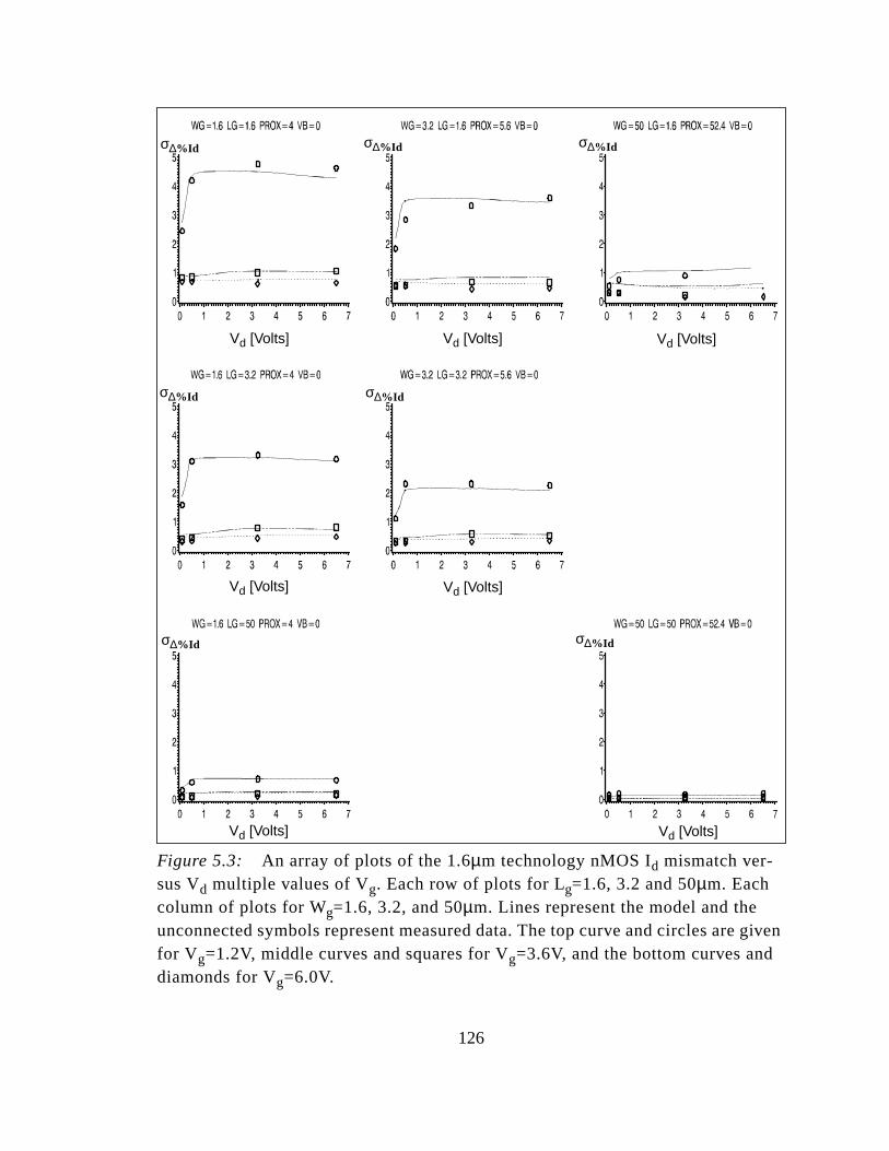
given
.
Figure 5.3: An array of plots of the 1.6µm technology nMOS Id mismatch ver-sus Vd multiple values of Vg. Each row of plots for Lg=1.6, 3.2 and 50µm. Eachcolumn of plots for Wg=1.6, 3.2, and 50µm. Lines represent the model and theunconnected symbols represent measured data. The top curve and circles arefor Vg=1.2V, middle curves and squares for Vg=3.6V, and the bottom curves anddiamonds for Vg=6.0V.
σ∆%Idσ∆%Idσ∆%Id
σ∆%Id σ∆%Id
σ∆%Idσ∆%Id
Vd [Volts] Vd [Volts]Vd [Volts]
Vd [Volts] Vd [Volts]
Vd [Volts]Vd [Volts]
126
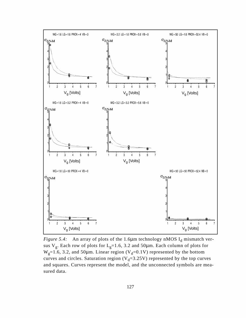
mea-
Figure 5.4: An array of plots of the 1.6µm technology nMOS Id mismatch ver-sus Vg. Each row of plots for Lg=1.6, 3.2 and 50µm. Each column of plots forWg=1.6, 3.2, and 50µm. Linear region (Vd=0.1V) represented by the bottomcurves and circles. Saturation region (Vd=3.25V) represented by the top curvesand squares. Curves represent the model, and the unconnected symbols aresured data.
σ∆%Id σ∆%Id σ∆%Id
σ∆%Idσ∆%Id
σ∆%Id σ∆%Id
Vg [Volts] Vg [Volts] Vg [Volts]
Vg [Volts]Vg [Volts]
Vg [Volts]Vg [Volts]
127
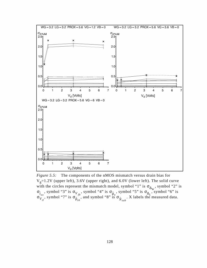
is
Figure 5.5: The components of the nMOS mismatch versus drain bias forVg=1.2V (upper left), 3.6V (upper right), and 6.0V (lower left). The solid curvewith the circles represent the mismatch model, symbol “1” is , symbol “2”
, symbol “3” is , symbol “4” is , symbol “5” is , symbol “6” is, symbol “7” is , and symbol “8” is . X labels the measured data.
O
O O O
1 1 1 1
22 2 2
3
3 33
4 4 4 4
5 5 5 5
6 6 6 67 7 7 7
88 8 8 O O
O O
1 1 1 12 2 2 23 3
3 3
4 4 4 4
5 5 5 5
6 6 6 67 7 7 78 8 8 8
O O O O
1 1 1 12 2 2 23 3 3 34 4 4 4
5 5 5 5
6 6 6 67 7 7 78 8 8 8
σ∆%Id σ∆%Id
σ∆%Id
Vd [Volts] Vd [Volts]
Vd [Volts]
σ∆Wσ tox
σV fbσµo
σ∆LσVtl
σρshσ
Nsub
128
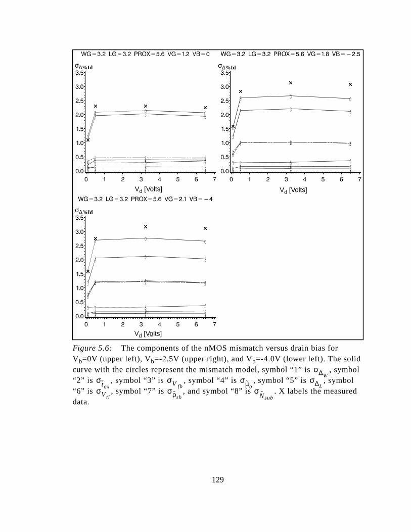
bol
Figure 5.6: The components of the nMOS mismatch versus drain bias forVb=0V (upper left), Vb=-2.5V (upper right), and Vb=-4.0V (lower left). The solidcurve with the circles represent the mismatch model, symbol “1” is , sym“2” is , symbol “3” is , symbol “4” is , symbol “5” is , symbol“6” is , symbol “7” is , and symbol “8” is . X labels the measureddata.
O
O O O
1 1 1 12 2 2 2
3
3 3 3
4 4 4 4
5 5 5 56 6 6 67 7 7 78
8 8 8
O
O O O
1 1 1 1
2
2 2 23
3 3 3
4 4 4 4
5 5 5 56 6 6 67 7 7 7
8
8 8 8
O
O O O
1 1 1 1
2
2 2 23
3 3 3
4 4 4 4
5 5 5 56 6 6 67 7 7 7
8
8 8 8
σ∆%Id σ∆%Id
σ∆%Id
Vd [Volts] Vd [Volts]
Vd [Volts]
σ∆Wσ tox
σV fbσµo
σ∆LσVtl
σρshσ
Nsub
129
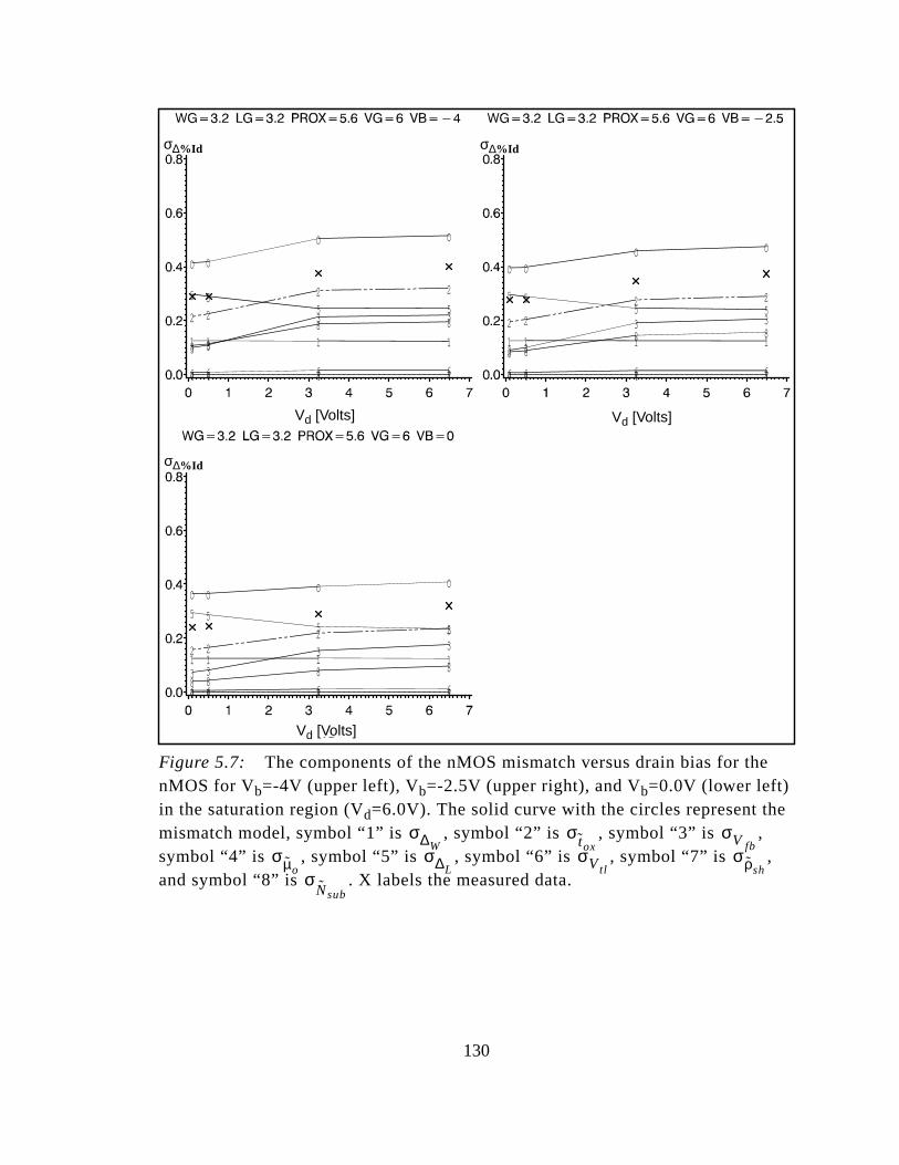
e
Figure 5.7: The components of the nMOS mismatch versus drain bias for thenMOS for Vb=-4V (upper left), Vb=-2.5V (upper right), and Vb=0.0V (lower left)in the saturation region (Vd=6.0V). The solid curve with the circles represent thmismatch model, symbol “1” is , symbol “2” is , symbol “3” is ,symbol “4” is , symbol “5” is , symbol “6” is , symbol “7” is ,and symbol “8” is . X labels the measured data.
O O
O O
1 1 1 1
2 2
2 2
3 3
3 3
4 4 4 4
5 55 5
6 6 6 67 7 7 7
8 8
8 8
O OO O
1 1 1 1
2 2
2 2
3 3
3 3
4 4 4 4
5 55 5
6 6 6 67 7 7 7
8 88 8
O O O O
1 1 1 12 2
2 2
3 3
3 3
4 4 4 4
5 55 5
6 6 6 67 7 7 78 8
8 8
σ∆%Id σ∆%Id
σ∆%Id
Vd [Volts] Vd [Volts]
Vd [Volts]
σ∆Wσ tox
σV fbσµo
σ∆LσVtl
σρshσ
Nsub
130
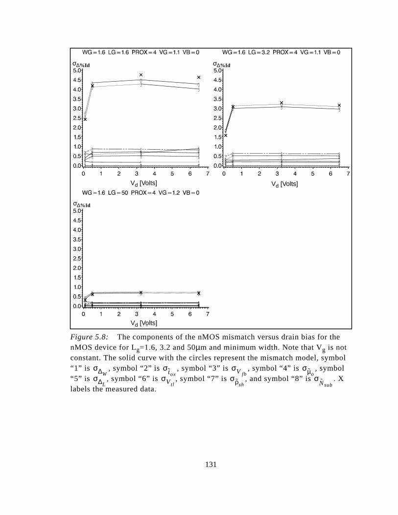
bol
Figure 5.8: The components of the nMOS mismatch versus drain bias for thenMOS device for Lg=1.6, 3.2 and 50µm and minimum width. Note that Vg is notconstant. The solid curve with the circles represent the mismatch model, sym“1” is , symbol “2” is , symbol “3” is , symbol “4” is , symbol“5” is , symbol “6” is , symbol “7” is , and symbol “8” is . Xlabels the measured data.
O
O OO
1 1 1 1
22 2 2
3
3 33
4 4 4 4
5 5 55
66 6 6
7 7 7 78
8 8 8
O
O O O
1 1 1 12 2 2 2
3
3 3 3
4 4 4 45 5 5 56 6 6 67 7 7 78
8 8 8
OO O O
1 1 1 12 2 2 23
3 3 3
4 4 4 45 5 5 56 6 6 67 7 7 78 8 8 8
σ∆%Id σ∆%Id
σ∆%Id
Vd [Volts] Vd [Volts]
Vd [Volts]
σ∆Wσ tox
σV fbσµo
σ∆LσVtl
σρshσ
Nsub
131
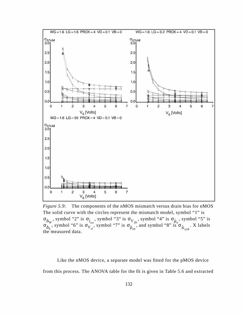
S
e
ed
Figure 5.9: The components of the nMOS mismatch versus drain bias for nMOThe solid curve with the circles represent the mismatch model, symbol “1” is
, symbol “2” is , symbol “3” is , symbol “4” is , symbol “5” is, symbol “6” is , symbol “7” is , and symbol “8” is . X labels
the measured data.
Like the nMOS device, a separate model was fitted for the pMOS devic
from this process. The ANOVA table for the fit is given in Table 5.6 and extract
OOO
O
OO O OOOO O O O O OOO O
1111 1 1 1 1 1111 1 1 1 1 111 1
22222 2 2 2 2222 2 2 2 2 222 2
333
3
33
3 3333 3 3 3 3 333 34444 4 4 4 4 4444 4 4 4 4 444 4
5555 5 5 5 5 5555 5 5 5 5 555 5
66666 6 6 6 6666 6 6 6 6 666 67777 7 7 7 7 7777 7 7 7 7 777 7
88888 8 8 8 8888 8 8 8 8 888 8
O
OOO
O
OO O OOOO O O O O OOO O
1111 1 1 1 1 1111 1 1 1 1 111 1
2222 2 2 2 2 2222 2 2 2 2 222 2
3
333
3
33
3 3333 3 3 3 3 333 34444 4 4 4 4 4444 4 4 4 4 444 4
5555 5 5 5 5 5555 5 5 5 5 555 56666 6 6 6 6 6666 6 6 6 6 666 67777 7 7 7 7 7777 7 7 7 7 777 7
8888 8 8 8 8 8888 8 8 8 8 888 8
OOOO O O O O OOOO O O O O OOO O1 111 1 1 1 1 1111 1 1 1 1 111 12 222 2 2 2 2 2222 2 2 2 2 222 2
3333
3 3 3 3 3333 3 3 3 3 333 34 444 4 4 4 4 4444 4 4 4 4 444 45 555 5 5 5 5 5555 5 5 5 5 555 56 666 6 6 6 6 6666 6 6 6 6 666 67 777 7 7 7 7 7777 7 7 7 7 777 78 888 8 8 8 8 8888 8 8 8 8 888 8
σ∆%Id σ∆%Id
σ∆%Id
Vg [Volts] Vg [Volts]
Vg [Volts]
σ∆Wσ tox
σV fbσµo
σ∆LσVtl
σρshσ
Nsub
132
re
om-
es
etra-
g a
atter
the
ick-
and
pant
n.
f
.
gain
coefficient are given in Table 5.7. Qualitatively and quantitatively, the results we
similar to the nMOS device.
Having similar devices on the same silicon presents an opportunity to c
bine like features of the two devices. Both the nMOS and the pMOS gate oxid
are grown at the same time, and aside from slight deviation due to boron pen
tion in the gate oxide or phosphorus modification of the Si / SiO2 interface, the
mismatches for the gate oxide thickness component should be the same. The
nMOS and pMOS mismatch parameters can be simultaneously extracted usin
shared gate oxide thickness parameter. Figure 5.10 shows the correlation sc
plots for the nMOS device after combining the sensitivities. In comparison to
correlation scatter plot in Figure 5.2, the correlation between the gate oxide th
ness and the substrate dopant concentration has been lessened. The pMOS
nMOS devices having independently determined variations in the substrate do
concentration but have a shared variation in the gate oxide thickness variatio
The ANOVA for the combined fit is given in Table 5.8 which shows little, i
any compromise in the fit versus the ANOVA tables in Table 5.4 and Table 5.6
The extracted parameters for both sets of extractions are given in Table 5.9. A
there is not a profound shift in the values of these parameters.
133
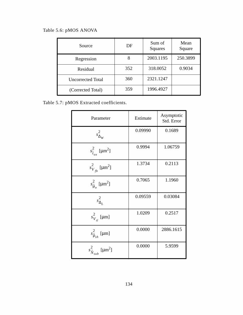
Table 5.6: pMOS ANOVA
Table 5.7: pMOS Extracted coefficients.
Source DFSum ofSquares
MeanSquare
Regression 8 2003.1195 250.3899
Residual 352 318.0052 0.9034
Uncorrected Total 360 2321.1247
(Corrected Total) 359 1996.4927
Parameter EstimateAsymptoticStd. Error
0.09990 0.1689
[µm2]0.9994 1.06759
[µm2]1.3734 0.2113
[µm2]0.7065 1.1960
0.09559 0.03084
[µm]1.0209 0.2517
[µm]0.0000 2886.1615
[µm2]0.0000 5.9599
s∆W
2
stox
2
sV fb
2
sµo
2
s∆L
2
sVtl
2
sρsh
2
sNsub
2
134
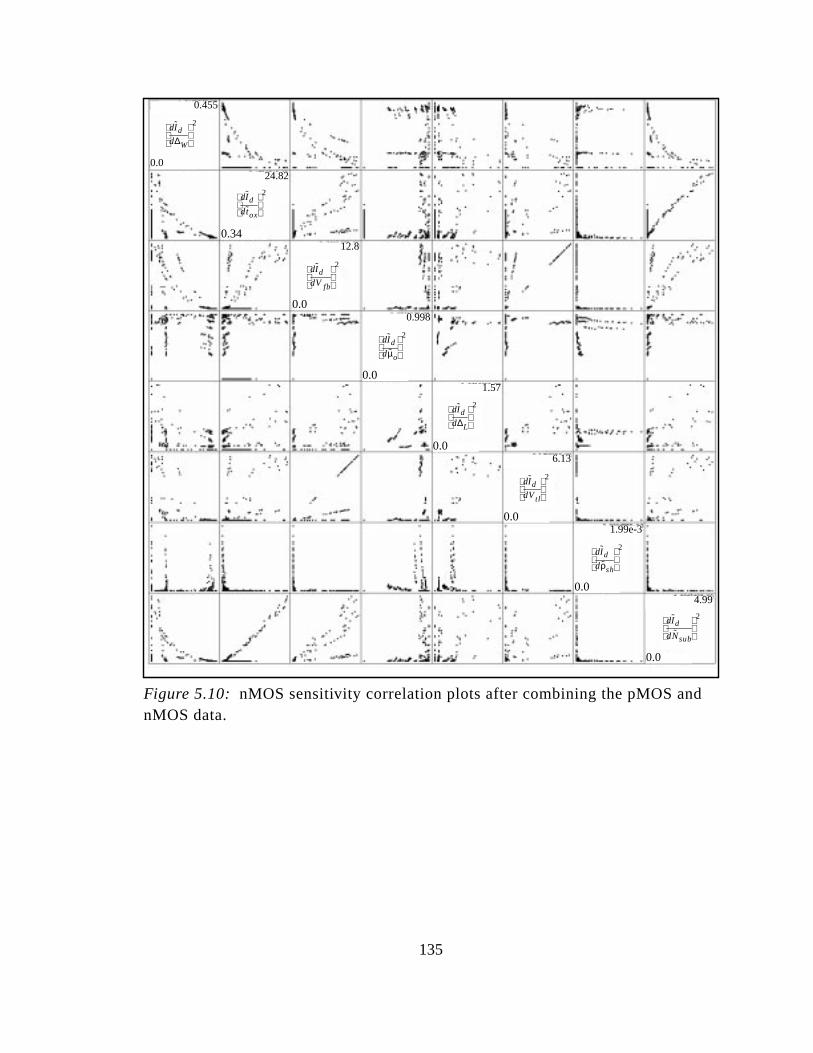
.
Figure 5.10: nMOS sensitivity correlation plots after combining the pMOS andnMOS data.
∆Wd
dId
2
toxd
dId
2
V fbd
dId
2
µod
dId
2
∆Ld
dId
2
Vtld
dId
2
ρshd
dId
2
Nsubd
dId
2
0.455
0.0
0.34
0.0
0.0
0.0
0.0
0.0
0.0
24.82
12.8
0.998
1.57
6.13
1.99e-3
4.99
135
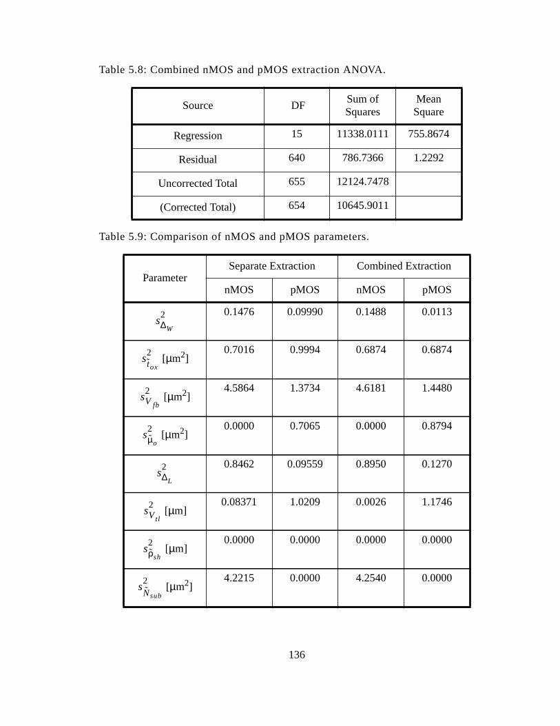
Table 5.8: Combined nMOS and pMOS extraction ANOVA.
Table 5.9: Comparison of nMOS and pMOS parameters.
Source DFSum ofSquares
MeanSquare
Regression 15 11338.0111 755.8674
Residual 640 786.7366 1.2292
Uncorrected Total 655 12124.7478
(Corrected Total) 654 10645.9011
ParameterSeparate Extraction Combined Extraction
nMOS pMOS nMOS pMOS
0.1476 0.09990 0.1488 0.0113
[µm2]0.7016 0.9994 0.6874 0.6874
[µm2]4.5864 1.3734 4.6181 1.4480
[µm2]0.0000 0.7065 0.0000 0.8794
0.8462 0.09559 0.8950 0.1270
[µm]0.08371 1.0209 0.0026 1.1746
[µm]0.0000 0.0000 0.0000 0.0000
[µm2]4.2215 0.0000 4.2540 0.0000
s∆W
2
stox
2
sV fb
2
sµo
2
s∆L
2
sVtl
2
sρsh
2
sNsub
2
136
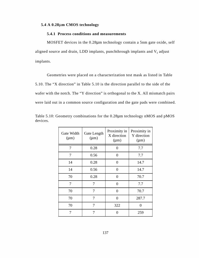
f
ble
s
ined.
5.4 A 0.28µm CMOS technology
5.4.1 Process conditions and measurements
MOSFET devices in the 0.28µm technology contain a 5nm gate oxide, sel
aligned source and drain, LDD implants, punchthrough implants and Vt adjust
implants.
Geometries were placed on a characterization test mask as listed in Ta
5.10. The “X direction” in Table 5.10 is the direction parallel to the side of the
wafer with the notch. The “Y direction” is orthogonal to the X. All mismatch pair
were laid out in a common source configuration and the gate pads were comb
Table 5.10: Geometry combinations for the 0.28µm technology nMOS and pMOSdevices.
Gate Width(µm)
Gate Length(µm)
Proximity inX direction
(µm)
Proximity inY direction
(µm)
7 0.28 0 7.7
7 0.56 0 7.7
14 0.28 0 14.7
14 0.56 0 14.7
70 0.28 0 70.7
7 7 0 7.7
70 7 0 70.7
70 7 0 287.7
70 7 322 0
7 7 0 259
137

on
ses
and
re
sion
.
Measurements were performed on 32 sites of a single wafer in a comm
source configuration. Biases were applied as listed in Table 5.11. The drain bia
were chosen to sample the mismatch in the linear region, the saturation region
in the intermediate region between linear and saturation. The gate biases we
selected to sample the above the threshold voltage, and into the strong inver
region.A correlation plot of the nMOS sensitivity parameters is given in Figure
5.11. In this case, there is more scatter in the plot of versus
Table 5.11: Bias combinations applied to the 0.28µm nMOS device. All possiblecombinations of the listed biases were applied. A similar set of biases wereapplied to the pMOS but with the signs reversed.
Biases
Drain 0.1, 0.23, 1.8, 2.5V
Gate (Vg@ peak gm), 1.25, 2.5V
Source 0.0V
Bulk 0.0, -1.25, -2.5V
toxd
dId
2
Nsubd
dId
2
138
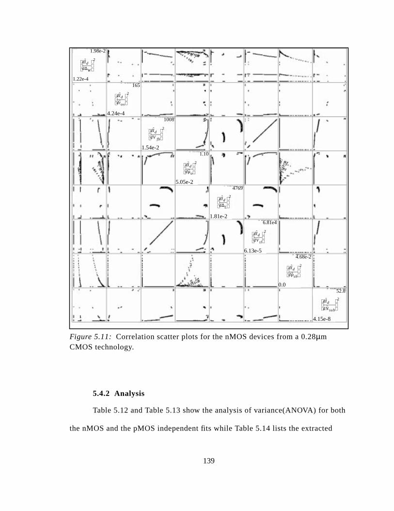
oth
.
Figure 5.11: Correlation scatter plots for the nMOS devices from a 0.28µmCMOS technology.
5.4.2 Analysis
Table 5.12 and Table 5.13 show the analysis of variance(ANOVA) for b
the nMOS and the pMOS independent fits while Table 5.14 lists the extracted
∆Wd
dId
2
toxd
dId
2
V fbd
dId
2
µod
dId
2
∆Ld
dId
2
Vtld
dId
2
ρshd
dId
2
Nsubd
dId
2
1.98e-2
1.22e-4
4.24e-4
1.54e-2
5.05e-2
1.81e-2
6.13e-5
0.0
4.15e-8
165
1008
1.10
4769
6.81e4
4.68e-2
52.8
139

ed
eters
, it
dis-
ble
e.
for
ow.
r
ents
d be
coefficients. Both fits appear to be good. The nMOS and pMOS fits are combin
as prescribed in Section 5.3.2 and the resultant ANOVA and extracted param
are given in Table 5.15 and Table 5.16. Comparing Table 5.14 with Table 5.16
is apparent that the nMOS parameters have not changed much but the large
crepancy in mismatch variance between the nMOS and pMOS devices in Ta
5.14 is brought into line in Table 5.16 by adjusting the mismatch varianc
The extraordinarily large values in the and estimates can be
explained by considering the extraction method. If the SPICE model parameter
the substrate dopant concentration is underestimated, the sensitivity will be l
However, the extracted parameter from the BPV technique will compensate fo
this. Hence, caution should be exercised when reviewing the extracted coeffici
in Table 5.15 or Table 5.16. The significance of each process parameter shoul
derived from the components plots, not from the relative magnitudes of the
extracted parameters.
Table 5.12: 0.28µm technology nMOS ANOVA.
Source DFSum ofSquares
MeanSquare
Regression 16 69.046 4.315
Residual 224 0.482 0.002
Uncorrected Total 240 69.528
(Corrected Total) 239 42.816
tox
Nsub
stox
2sNsub
2
140
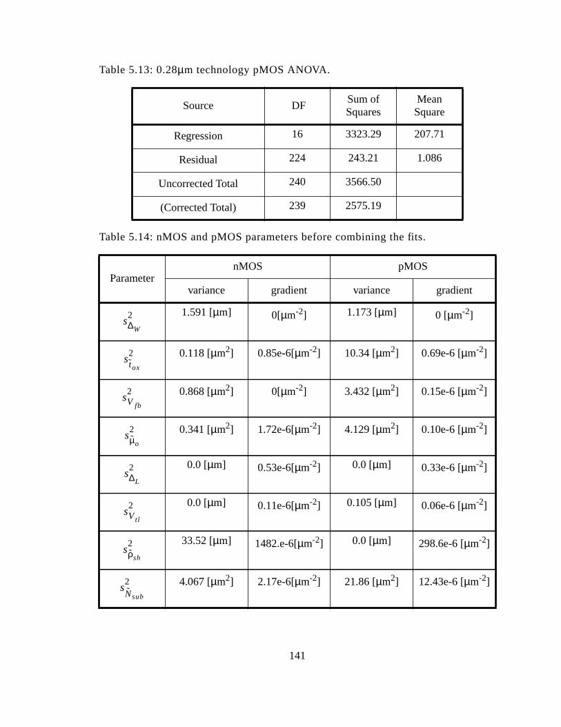
Table 5.13: 0.28µm technology pMOS ANOVA.
Table 5.14: nMOS and pMOS parameters before combining the fits.
Source DFSum ofSquares
MeanSquare
Regression 16 3323.29 207.71
Residual 224 243.21 1.086
Uncorrected Total 240 3566.50
(Corrected Total) 239 2575.19
ParameternMOS pMOS
variance gradient variance gradient
1.591 [µm] 0[µm-2] 1.173 [µm] 0 [µm-2]
0.118 [µm2] 0.85e-6[µm-2] 10.34 [µm2] 0.69e-6 [µm-2]
0.868 [µm2] 0[µm-2] 3.432 [µm2] 0.15e-6 [µm-2]
0.341 [µm2] 1.72e-6[µm-2] 4.129 [µm2] 0.10e-6 [µm-2]
0.0 [µm] 0.53e-6[µm-2] 0.0 [µm] 0.33e-6 [µm-2]
0.0 [µm] 0.11e-6[µm-2] 0.105 [µm] 0.06e-6 [µm-2]
33.52 [µm] 1482.e-6[µm-2] 0.0 [µm] 298.6e-6 [µm-2]
4.067 [µm2] 2.17e-6[µm-2] 21.86 [µm2] 12.43e-6 [µm-2]
s∆W
2
stox
2
sV fb
2
sµo
2
s∆L
2
sVtl
2
sρsh
2
sNsub
2
141

OS
Table 5.15: ANOVA for the combined nMOS and pMOS fit.
Table 5.16: Comparison of nMOS and pMOS parameters with a combined nMand pMOS fit.
Source DFSum ofSquares
MeanSquare
Regression 30 3347.487 111.583
Residual 450 288.537 0.641
Uncorrected Total 480 3636.024
(Corrected Total) 479 2964.291
ParameternMOS pMOS
variance gradient variance gradient
1.6 [µm] 18.96e-6 [µm-2] 6.780 [µm] 23.69e-6 [µm-2]
0.643 [µm2] 0.33e-6 [µm-2] 0.643 0.33e-6 [µm-2]
0.771 [µm2] 0.07e-6 [µm-2] 3.797 [µm2] 0.17e-6 [µm-2]
0.158 [µm2] 0.83e-6 [µm-2] 5.579 [µm2] 0.24e-6 [µm-2]
0.0 [µm] 0.39e-6 [µm-2] 0.026 [µm] 0.35e-6 [µm-2]
0.0 [µm] 0.08e-6 [µm-2] 0.105 [µm] 0.05e-6 [µm-2]
35.596 [µm] 833.7e-6 [µm-2] 0.0 [µm] 475e-6 [µm-2]
4.0 [µm2] 1.17e-6 [µm-2] 64.333 [µm2] 13.31e-6 [µm-2]
s∆W
2
stox
2
sV fb
2
sµo
2
s∆L
2
sVtl
2
sρsh
2
sNsub
2
142

im-
ook-
rger
flat-
.
or-
be
ger
of
ns
bias.
oma-
Plots of the Id mismatch versus the drain bias for two values of Vg are
given in Figure 5.12. Each plot in Figure 5.12 is given for a unique geometry, s
ilar to the plots in Figure 5.3. Two phenomena are apparent in Figure 5.12. L
ing down the first column of plots, the top curve (low Vg) is not monotonic across
the geometries as described by the Pelgrom model and its derivatives. For la
gate biases (the bottom curves in each plot) the trend over geometry seems to
ten for minimum geometries which is not accounted for in the Pelgrom model
The Pelgrom model predicts that mismatch variance should be inversely prop
tional to gate area which means that the largest changes in mismatch should
observed around the minimum gate length. This trend is still apparent for a lar
gate width, as shown in the second column of plots in Figure 5.12.
As a further investigative tool, the plots of Id mismatch versus drain bias
are repeated in Figure 5.13 for the smallest gate width but this time the array
plots is arranged by variations in the gate length and the bulk bias. The colum
separate the three gate lengths and the rows separate the three values of bulk
Here, it can be observed that an increase in the bulk bias exacerbates the an
lous trend in mismatch over gate lengths, which implicates the body effect,
through Nsub and tox in the Id mismatch.
143

-
is
is
e
row
ts
bulk
flat-
ts),
The
chan-
,
h. As
.
To more clearly see the trend of Id mismatch over multiple gate lengths,
Figure 5.13 was again rearranged to plot Id mismatch versus gate length for multi
ple drain and bulk biases in Figure 5.14. Each column of plots in Figure 5.14
given for a value of bulk bias, and the drain biases are grouped by rows. In th
plot it is apparent that the anomalous effect over gate lengths is worst for larg
bulk and drain biases but with a low gate voltage.
The process and geometry components to the mismatch plots in the top
of plots in Figure 5.14 are broken down in Figure 5.15. The bottom row of plo
behave roughly as expected, with the Id mismatch improving asymptotically with
increase gate area. The right-most plot on the top row which contains a zero
bias and a small gate voltage, shows only a dominant mismatch caused by the
band voltage. As the bulk bias is increased (moving right to left across the plo
the substrate dopant concentration begins to show up through the body effect.
anomalous trend over gate lengths can be explained by considering the short
nel effect [37]. As the gate length decreases, the depletion regions from the
source/bulk and drain/bulk junctions deplete part of the region under the gate
thereby causing the threshold voltage to decrease with decreasing gate lengt
the threshold voltage drops, the gate overdrive at a fixed Vgs increases, and the Id
mismatch becomes less susceptible to the threshold voltage mismatch per Eq
(2.7) and Eq. (5.11).
144
he
ig-
11).
lk
bias.
at-
r
orse
to
n
e
e
is-
ance
tion
The second interesting phenomena in Figure 5.12 is the increase in Id mis-
match for low drain voltage and high gate voltage and short gate lengths, to t
point where the two Vg curves in the in the upper right plot cross. This trend is
apparent for all of the minimum gate length devices in the first row of plots in F
ure 5.12. This trend in gate voltage counters the derived relationship in Eq. (5.
The first row of plot in Figure 5.12 is plotted for each of the three values of bu
bias in Figure 5.16. The crossing phenomena decreases with increasing bulk
The Id mismatch is plotted against the gate width in Figure 5.17 for the s
uration region (first row of plots) and the linear region (second row of plots) fo
the three different gate widths. The anomalous trend in gate bias becomes w
for increasing gate width particularly in the linear region. As the bulk bias
decreases, the Id mismatch between the two gate biases narrows. Also, the Id mis-
match degrades with increasing gate width.
The mismatch component plots in Figure 5.18 provide key information
understanding this trend over geometry. For low gate voltages in the saturatio
region the mismatch over the gate widths is dominated by the flat band voltag
mismatch with a gradual increase in the and the Vtl mismatch gradients for
wider MOSFETs in the top left plot of Figure 5.18. When the device enters th
linear region, in the lower left plot of Figure 5.18, we see that the increase in m
match is caused by domination from the source sheet resistance. This domin
of the series resistance is even more apparent in the transition from the satura
∆L
145

of
rela-
rse
, but
e
in
ent
rms
the
or
ar to
to the linear region for large gate biases as shown in the two right-hand plots
Figure 5.18. As the gate bias increases, the channel conductance contributes
tively less to the overall output conductance, thereby increasing the Id mismatch
dependence on the series resistance. If the series resistance mismatch is wo
than the intrinsic MOSFET mismatch, then the Id mismatch will increase as the
gate bias increases. This is consistent with the extracted coefficients from the
0.28µm nMOS device ( =33.52) and the 1.6µm nMOS device ( =0.0). The
effect of the series resistance mismatch is only apparent for short gate lengths
contributes more for wider gate widths due to the gradient effect in the
source/drain sheet resistance mismatch.
Finally for the 0.28µm technology nMOS devices, the mismatch plots ar
shown in Figure 5.19 for the pairs of devices with large separation distances
two orthogonal directions. These plots confirm that the gradient effect is appar
in the mismatch standard deviation and that the gradients, when modeled in te
of process and geometry parameters, can predict the mismatch quite well.
Figure 5.20 shows mismatch over drain and gate bias and geometry for
pMOS device in the 0.28µm technology and is similar in layout to Figure 5.12.
Mismatch values for this device are larger than the nMOS device. The trend f
mismatch over drain and gate bias and across geometries is qualitatively simil
the other MOSFETs. The source/drain sheet resistance mismatch that was
ρsh ρsh
146

esis-
observed in the nMOS device is not apparent due to higher relative channel rtance on a pMOS device.
147
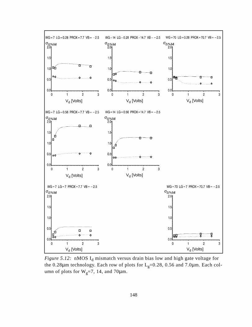
r
Figure 5.12: nMOS Id mismatch versus drain bias low and high gate voltage fothe 0.28µm technology. Each row of plots for Lg=0.28, 0.56 and 7.0µm. Each col-umn of plots for Wg=7, 14, and 70µm.σ∆%Id σ∆%Id σ∆%Id
σ∆%Id σ∆%Id
σ∆%Idσ∆%Id
Vd [Volts] Vd [Volts] Vd [Volts]
Vd [Volts] Vd [Volts]
Vd [Volts] Vd [Volts]
148

Figure 5.13: An array of plots of Id mismatch versus Vd for the nMOS devicewith Wg=7µm. Each column of plots is given for Lg=0.28, 0.56, and 7µm. Eachrow is given for Vb=0,-1.25, -2.5V. In each plot the low Vg value is the top curve.
σ∆%Id σ∆%Id σ∆%Id
σ∆%Idσ∆%Idσ∆%Id
σ∆%Id σ∆%Id σ∆%Id
Vd [Volts] Vd [Volts] Vd [Volts]
Vd [Volts] Vd [Volts] Vd [Volts]
Vd [Volts] Vd [Volts] Vd [Volts]
149
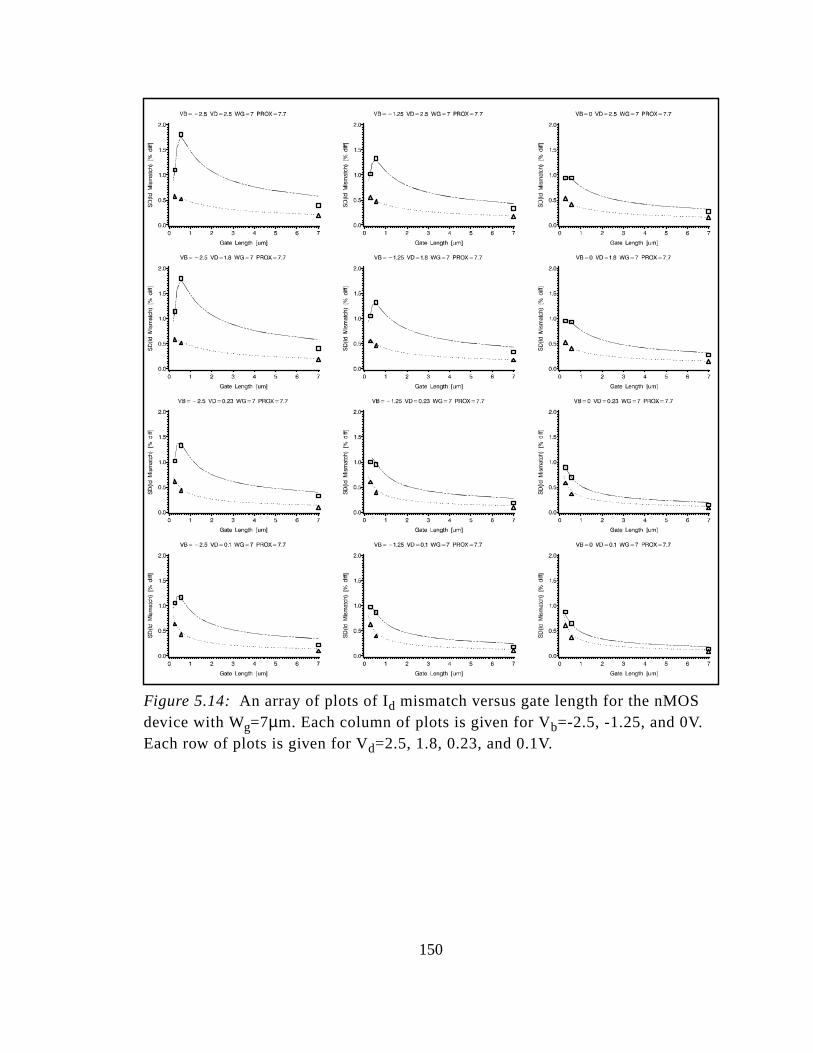
Figure 5.14: An array of plots of Id mismatch versus gate length for the nMOSdevice with Wg=7µm. Each column of plots is given for Vb=-2.5, -1.25, and 0V.Each row of plots is given for Vd=2.5, 1.8, 0.23, and 0.1V.
150
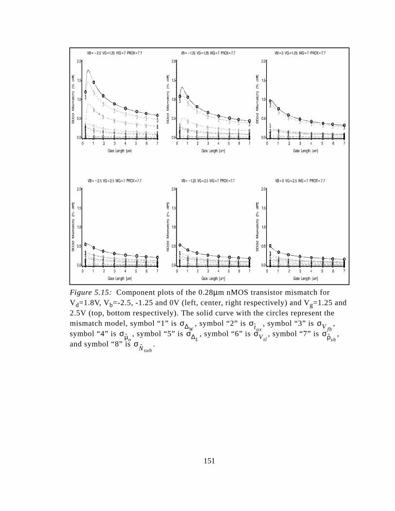
Figure 5.15: Component plots of the 0.28µm nMOS transistor mismatch forVd=1.8V, Vb=-2.5, -1.25 and 0V (left, center, right respectively) and Vg=1.25 and2.5V (top, bottom respectively). The solid curve with the circles represent themismatch model, symbol “1” is , symbol “2” is , symbol “3” is ,symbol “4” is , symbol “5” is , symbol “6” is , symbol “7” is ,and symbol “8” is .
1111 1 1 1 1 1 111
222 2 2 2 2 2 2 222
333 3 3 3 3 3 3 333444 4 4 4 4 4 4 444555 5 5 5 5 5 5 555666 6 6 6 6 6 6 666777 7 7 7 7 7 7 777888
8 8 8 8 8 8 888
1111 1 1 1 1 1 111
222 2 2 2 2 2 2 222
3333
33
3 3 3 333
444 4 4 4 4 4 4 444555 5 5 5 5 5 5 555666 6 6 6 6 6 6 666777 7 7 7 7 7 7 777
888
88
8 8 8 8 888
1111 1 1 1 1 1 111
222 2 2 2 2 2 2 222
3333 3 3 3 3 3 333444 4 4 4 4 4 4 444555 5 5 5 5 5 5 555666 6 6 6 6 6 6 666777 7 7 7 7 7 7 7778888 8 8 8 8 8 888
1111 1 1 1 1 1 111
222 2 2 2 2 2 2 222
333 33
3 3 3 3 333444 4 4 4 4 4 4 444555 5 5 5 5 5 5 555666 6 6 6 6 6 6 666777 7 7 7 7 7 7 777888
88 8 8 8 8 888
1111 1 1 1 1 1 111
222 2 2 2 2 2 2 222
3333 3 3 3 3 3 333444 4 4 4 4 4 4 444555 5 5 5 5 5 5 555666 6 6 6 6 6 6 666777 7 7 7 7 7 7 777888 8 8 8 8 8 8 888
1111 1 1 1 1 1 111
222 2 2 2 2 2 2 222
3333
33 3 3 3 333
444 4 4 4 4 4 4 444555 5 5 5 5 5 5 555666 6 6 6 6 6 6 666777 7 7 7 7 7 7 7778888 8 8 8 8 8 888
σ∆Wσ tox
σV fbσµo
σ∆LσVtl
σρshσ
Nsub
151
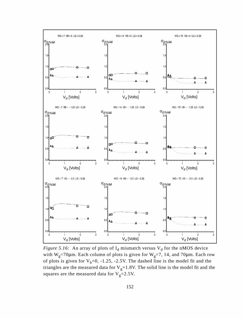
Figure 5.16: An array of plots of Id mismatch versus Vd for the nMOS devicewith Wg=70µm. Each column of plots is given for Wg=7, 14, and 70µm. Each rowof plots is given for Vb=0, -1.25, -2.5V. The dashed line is the model fit and thetriangles are the measured data for Vg=1.8V. The solid line is the model fit and thesquares are the measured data for Vg=2.5V.
σ∆%Id σ∆%Id σ∆%Id
σ∆%Idσ∆%Idσ∆%Id
σ∆%Id σ∆%Id σ∆%Id
Vd [Volts] Vd [Volts] Vd [Volts]
Vd [Volts] Vd [Volts] Vd [Volts]
Vd [Volts]Vd [Volts]Vd [Volts]
152
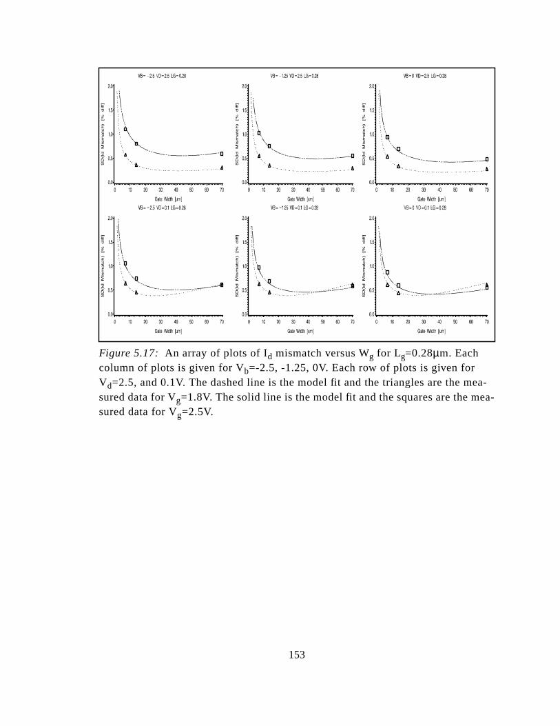
ea-ea-
Figure 5.17: An array of plots of Id mismatch versus Wg for Lg=0.28µm. Eachcolumn of plots is given for Vb=-2.5, -1.25, 0V. Each row of plots is given forVd=2.5, and 0.1V. The dashed line is the model fit and the triangles are the msured data for Vg=1.8V. The solid line is the model fit and the squares are the msured data for Vg=2.5V.
153
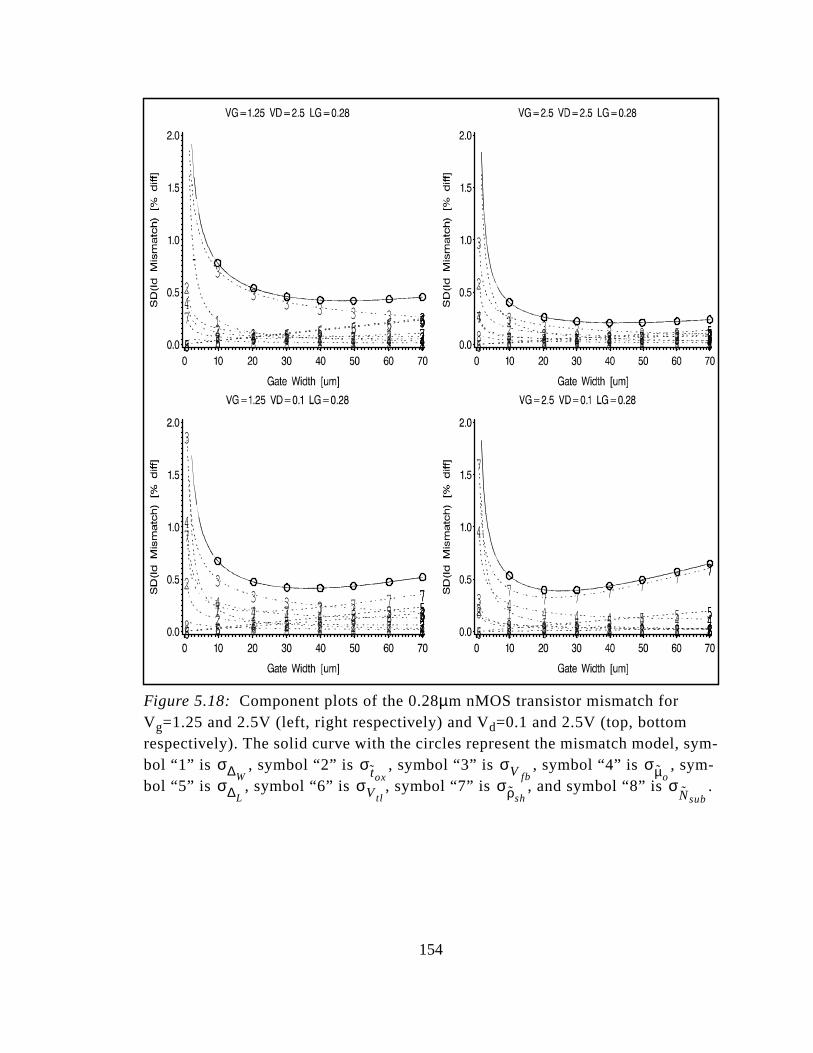
ym-
Figure 5.18: Component plots of the 0.28µm nMOS transistor mismatch forVg=1.25 and 2.5V (left, right respectively) and Vd=0.1 and 2.5V (top, bottomrespectively). The solid curve with the circles represent the mismatch model, sbol “1” is , symbol “2” is , symbol “3” is , symbol “4” is , sym-bol “5” is , symbol “6” is , symbol “7” is , and symbol “8” is .
11 1 1 1 1 111
2
2 2 2 2 2 2 222
3
33 3 3 3 3 333
4
4 4 4 4 4 4 4445 5 5 5 5 5 5 555
6 6 6 6 6 6 6 666
7
7 7 7 7 7 7 777
8 8 8 8 8 8 8 888
11 1 1 1 1 111
2
2 2 2 2 2 2 222
33 3 3 3 3 333
4
4 4 4 4 4 4 4445 5 5 5 5 5 5 5556 6 6 6 6 6 6 6667
7 7 7 7 7 7 7778 8 8 8 8 8 8 888
11 1 1 1 1 111
22 2 2 2 2 2 222
3
3 3 3 3 3 3 333
4
4 4 4 4 4 4 4445 5 5 5 5 5 5 5556 6 6 6 6 6 6 666
7
7 7 7 7 7 7 777
88 8 8 8 8 8 888
11 1 1 1 1 111
2
2 2 2 2 2 2 222
3
3 3 3 3 3 3 3334
4 4 4 4 4 4 4445 5 5 5 5 5 5 5556 6 6 6 6 6 6 6667
7 7 7 7 7 7 7778 8 8 8 8 8 8 888
σ∆Wσ tox
σV fbσµo
σ∆LσVtl
σρshσ
Nsub
154
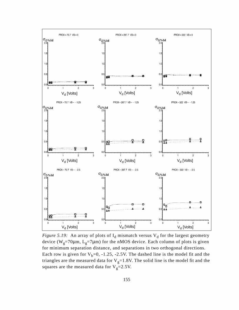
ns.e
Figure 5.19: An array of plots of Id mismatch versus Vd for the largest geometrydevice (Wg=70µm, Lg=7µm) for the nMOS device. Each column of plots is givefor minimum separation distance, and separations in two orthogonal directionEach row is given for Vb=0, -1.25, -2.5V. The dashed line is the model fit and thtriangles are the measured data for Vg=1.8V. The solid line is the model fit and thesquares are the measured data for Vg=2.5V.
σ∆%Id σ∆%Id σ∆%Id
σ∆%Idσ∆%Idσ∆%Id
σ∆%Id σ∆%Id σ∆%Id
Vd [Volts] Vd [Volts] Vd [Volts]
Vd [Volts]Vd [Volts]Vd [Volts]
Vd [Volts] Vd [Volts] Vd [Volts]
155
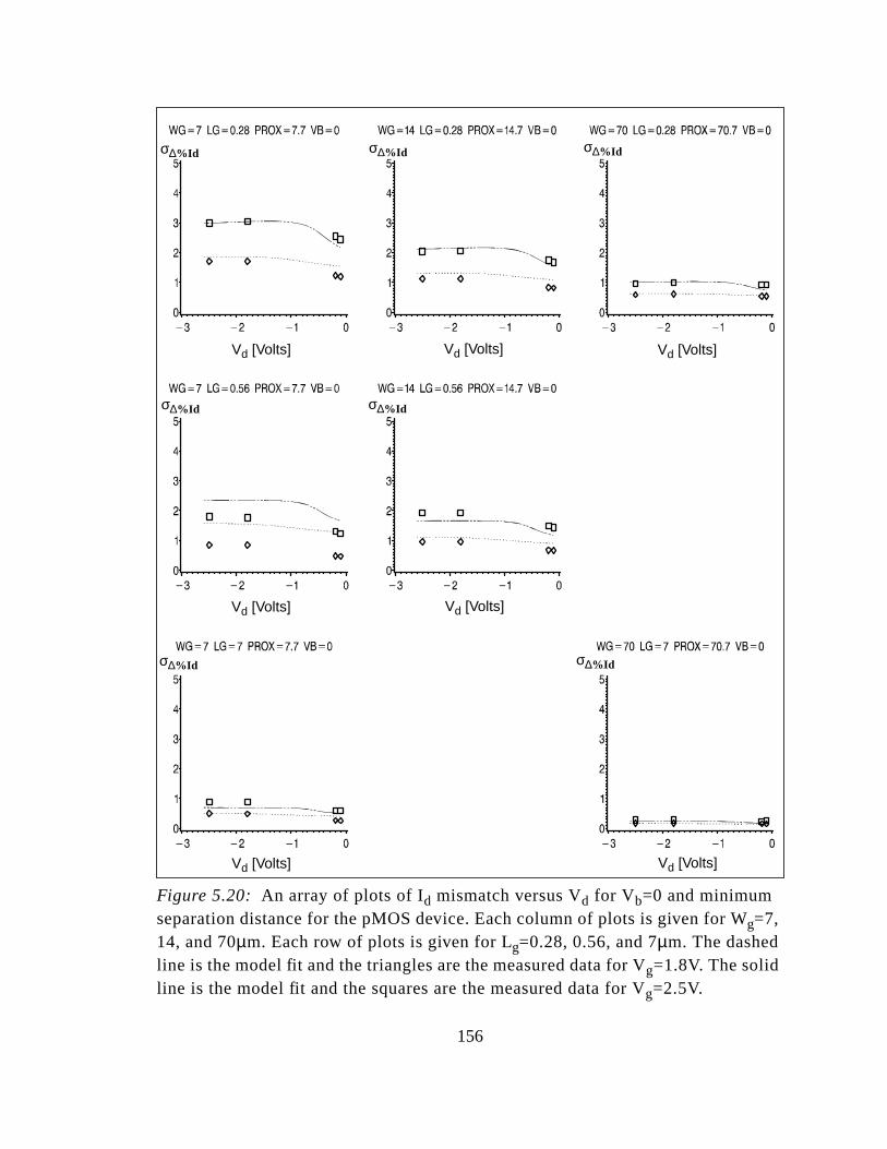
Figure 5.20: An array of plots of Id mismatch versus Vd for Vb=0 and minimumseparation distance for the pMOS device. Each column of plots is given for Wg=7,14, and 70µm. Each row of plots is given for Lg=0.28, 0.56, and 7µm. The dashedline is the model fit and the triangles are the measured data for Vg=1.8V. The solidline is the model fit and the squares are the measured data for Vg=2.5V.
σ∆%Id σ∆%Id σ∆%Id
σ∆%Idσ∆%Id
σ∆%Id σ∆%Id
Vd [Volts] Vd [Volts] Vd [Volts]
Vd [Volts] Vd [Volts]
Vd [Volts] Vd [Volts]
156

Figure 5.21: An array of plots of Id mismatch versus Vg for the pMOS device.Each column of plots is given for Wg=7, 14, and 70µm. Each row of plots is givenfor Lg=0.28, 0.56, and 7µm. Squares, dotted line denote Vd=1.8V, circles, solidline denote Vd=0.1V. Squares, circles are measured data, lines represent themodel.
σ∆%Id σ∆%Id σ∆%Id
σ∆%Idσ∆%Id
σ∆%Id σ∆%Id
Vg [Volts] Vg [Volts] Vg [Volts]
Vg [Volts] Vg [Volts]
Vg [Volts] Vg [Volts]
157
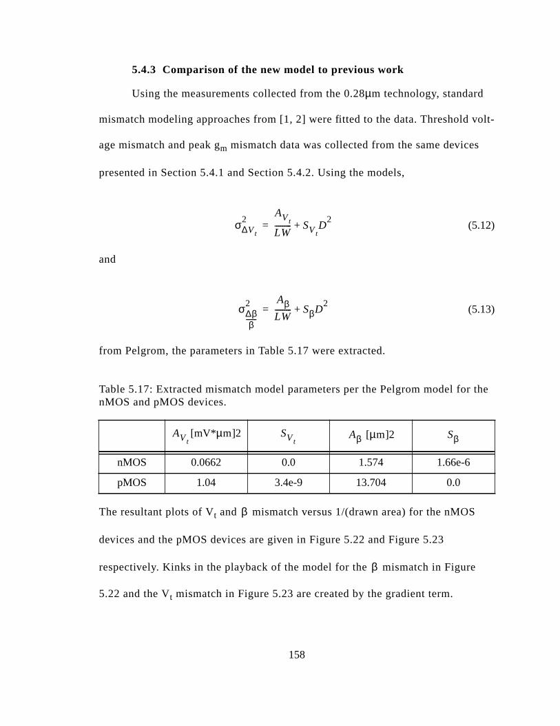
olt-
the
5.4.3 Comparison of the new model to previous work
Using the measurements collected from the 0.28µm technology, standard
mismatch modeling approaches from [1, 2] were fitted to the data. Threshold v
age mismatch and peak gm mismatch data was collected from the same devices
presented in Section 5.4.1 and Section 5.4.2. Using the models,
(5.12)
and
(5.13)
from Pelgrom, the parameters in Table 5.17 were extracted.
Table 5.17: Extracted mismatch model parameters per the Pelgrom model fornMOS and pMOS devices.
The resultant plots of Vt and mismatch versus 1/(drawn area) for the nMOS
devices and the pMOS devices are given in Figure 5.22 and Figure 5.23
respectively. Kinks in the playback of the model for the mismatch in Figure
5.22 and the Vt mismatch in Figure 5.23 are created by the gradient term.
[mV* µm]2 [µm]2
nMOS 0.0662 0.0 1.574 1.66e-6
pMOS 1.04 3.4e-9 13.704 0.0
σ∆Vt
2AVt
LW--------- SVt
D2
+=
σ∆ββ
-------
2 AβLW--------- SβD
2+=
AVtSVt
Aβ Sβ
β
β
158

the
on
V
d
ith
orse
job
on
w
The fits inFigure 5.22 and Figure 5.23 seem reasonable with the obvious
exception of the Vt mismatch curve in Figure 5.23. A geometrically consistent
explanation of the scatter is not readily apparent in the remaining plots. Using
model from [3, 39] for the prediction of the drain current mismatch as a functi
of Vt mismatch and mismatch,
(5.14)
gives the comparison plots of measured versus simulated Id mismatch data in
Figure 5.24, Figure 5.25, Figure 5.26, and Figure 5.27 were obtained. Thet
in Eq. (5.14) was measured from the SPICE model file. It should be note
that several publications[1, 65, 56] promote the use of just the Vt mismatch
as the single predictor of input offset voltage. That model is not shown w
a comparison to the measured data since it would be guaranteed to be w
than Eq. (5.14), and Eq. (5.14) serves as a satisfactory example of the
shortcomings of this approach.
As expected in Figure 5.24, the model in Eq. (5.14) does a reasonable
of predicting the Id mismatch in the saturation region since Eq. (5.14) is based
the simple Id relationship in the saturation region. The model is unable to follo
the improvement in mismatch in the linear region.
β
σI d
2
I d2
--------σβ
2
β2------
4σ∆Vt
2
Vgs Vt–( )-------------------------+=
159
the
the
.
4)
f.
sed
fit
con-
Eq. (5.14) is unable to predict the improvement in mismatch caused by
short channel effect, which leads to a dramatic over-prediction for the top on
left and center of Figure 5.24 and the left-most column of plots in Figure 5.25
The model over-predicts the mismatch by almost 100%. Qualitatively Eq. (5.1
has the correct trend over bulk biases in Figure 5.25 but quantitatively it is of
The increase in mismatch over the bulk bias is created by the increase in Vt which
increases the contribution to the Id mismatch in the second term of Eq. (5.14).
The convergence in Id mismatch across Vg for low values of Vd and wide
gate widths in the right hand column of plots in Figure 5.26 is also incorrectly
modeled by Eq. (5.14). This would be expected since the convergence is cau
the source series resistance mismatch which is not included in the model.
The Id mismatch for the large separation pairs at Vb=0 in top row of plots
in Figure 5.27 seems to fit fairly well. For increased bulk biases, however, the
does not the trend in the data since the gradient term in the substrate dopant
centration is not apparent.
A new modified POV approach using,
(5.15)σI d
2
I d2
--------Vt∂
∂I d
2
σ∆Vt
2=
160

27
I
d in
uce
edic-
k-
h
8
The
sis-
was implemented to explore how much improvement in the fit of Id mismatch can
be gained by using SPICE to numerically evaluate the partial derivative. This
approach mimics a statistical simulation implementation in SPICE. Eq.(5.15) is a
more generic form of the Vt dependence in the second term inEq. (5.14). The
comparable plots to Figure 5.24, Figure 5.25, Figure 5.26, and Figure 5.
are given in Figure 5.28, Figure 5.29, Figure 5.30, and Figure 5.31
respectively.
In Figure 5.28, Eq. (5.15) does a much better job of tracking the trend ind
mismatch from the linear to saturation regions since both regions are modele
SPICE. However, in the top three plots of Figure 5.28, the model tries to prod
the decrease in Id mismatch for the linear region in a situation where the linear
region mismatch improvement is offset by the increased contribution from the
series resistance mismatch. Most of the plots in Figure 5.28 show an under-pr
tion of the mismatch, presumably due to the neglect of the mobility, oxide thic
ness and geometry mismatch contributions that come through the mismatc
term.
Looking at the three plots in the left-most column of plots in Figure 5.2
and in the plots of Figure 5.29, the reverse short channel affect on Id mismatch is
apparent in the model since the SPICE model inherently includes this effect.
trend in mismatch across the bulk biases in Figure 5.29 is similar to the trend
observed in Figure 5.25 for the same reason as in Figure 5.25. The series re
β
161

the I
e
he
re
nd
es
s
ure
he
tance dependence is missing in Figure 5.30, as expected. The dependence ofd
mismatch on the gradient effect is completely missing in Figure 5.31 since th
gradient term coefficient for the nMOS Vt mismatch in Table 5.17 is zero. The
gradient was only apparent for the term for the nMOS device.
The model in Eq. (5.15) is extended to include the mismatch,
(5.16)
with both partial derivatives numerically evaluated by SPICE. The partial
derivative for was produced via deviations in the reference mobility term of t
SPICE model. Again, the comparable plots to Figure 5.24, Figure 5.25, Figu
5.26, and Figure 5.27 are given in Figure 5.32, Figure 5.33, Figure 5.34, a
Figure 5.35 respectively. The addition of mismatch allows the top curv
(Vg=1.8V) in the top row of plots in Figure 5.32 to flatten compared to
Figure 5.28 as per the series resistance mismatch. But the bottom curve
(Vg=2.5V) have curved upward too much to compensate since the
mismatch lacks the proper Vg dependence that is built into the extrinsic
resistance. The short channel affect on Id mismatch in Figure 5.32 and Figure
5.33 is the same as Figure 5.28 and Figure 5.29 since the Vt mismatch is the
same. Qualitatively, the trend for the series resistance contribution in Fig
5.34 is correct but quantitatively it is offset presumably due to a bias in t
β
β
σI d
2
I d2
--------Vt∂
∂I d
2
σ∆Vt
2
β∂
∂I d
2σβ2
β2------+=
β
β
β
162

t a
par-
.27
t in
ict-
plot
ther
s
s
by
sig-
n
least squares solution of and Vt mismatch versus an Id least squares
objective criteria. A BPV solution using Id mismatch and and Vt as SPICE
model mismatch parameters may improve this fit. The behavior for large
spaced pairs seems to have improved in Figure 5.35 although there is no
sufficient spread in Id mismatch for the two Vg values. Overall the fits in
Figure 5.32 through Figure 5.35 seem fairly encouraging.
The approach using Eq. (5.16) was repeated for the pMOS device. The
allel fit-comparison plots in Figure 5.24, Figure 5.25, Figure 5.26, and Figure 5
are given in Figure 5.36, Figure 5.37, Figure 5.38, and Figure 5.39. It is eviden
these plots that the mismatch model from Eq. (5.16) is significantly over-pred
ing the mismatch. In many of plots the mismatch model data has gone off the
since the mismatch axis range is preserved to maintain consistency with the o
plots. The model offset is worst for the smallest geometry devices. This seem
counterintuitive since the Vt mismatch plot in Figure 5.23 shows that the model i
under-predicting the data for the large geometry devices. The issue is clarified
looking at the scatter plots of Vt mismatch versus mismatch for both the nMOS
and pMOS devices in Figure 5.40. It is apparent from these plots that there is
nificant correlation between the Vt and mismatch for the pMOS device. This
means that the Id mismatch variance will be over-predicted since the correlatio
between the variables is accounted for twice, once in the Vt mismatch variance
and once in the mismatch variance. This means that the Id mismatch predicted
β
β
β
β
β
163

, the
ted
for
is
5.40
te
OS
ur-
con-
h
,
ss,
e
variance will be overestimated for the small geometries since the Vt mismatch
model is roughly close to the measured values. For the large geometry devices
under-prediction in the Vt mismatch is offset by the double count of the covari-
ance.
Physically the covariance can be explained by re-examining the extrac
coefficients from the BPV model in Table 5.14. This model inferred a variance
tox of 10.34, which is the second largest value in the table. The largest value
Nsub which is parametrically similar to tox. The parameter tox, physically appears
in both the term through the oxide capacitance and in the Vt mismatch.
The relative spreads and the correlations in the scatter plots in Figure
can be explained by considering the relationship between the surface substra
dopant concentration and the gate oxide thickness. For a pair of matched nM
devices, a slightly thicker gate oxide will leach more boron dopant from the s
face of the channel region. The increase in gate oxide thickness produces a
slightly higher threshold voltage but at the same time, the lower boron dopant
centration will decrease the threshold voltage. The two effects counteract eac
other, producing a tighter distribution in Figure 5.40(a). For the pMOS device
both the decrease in dopant concentration and increase in gate oxide thickne
constructively create a larger offset in the threshold voltage which leads to th
wider spread in the scatter plot in Figure 5.40(b).
β
164

heh
heh
Figure 5.22: Plots of Vt and mismatch for measured and predicted data for tPelgrom model on the nMOS device. “X’s” represent the measured data, eaclabeled by the geometry (W/L) and the solid line is the model.
Figure 5.23: Plots of Vt and mismatch for measured and predicted data for tPelgrom model on the pMOS device. “X’s” represent the measured data, eaclabeled by the geometry (W/L) and the solid line is the model.
7/0.28
7/0.56
14/0.28
14/0.56
70/0.28
7/7
70/7
7/0.28
7/0.56
14/0.28
14/0.5670/0.28
7/7
70/7
β
7/0.287/0.56
14/0.28
14/0.56
70/0.28
7/7
70/7
7/0.28
7/0.56
14/0.2814/0.56
70/0.28
7/7
70/7
β
165
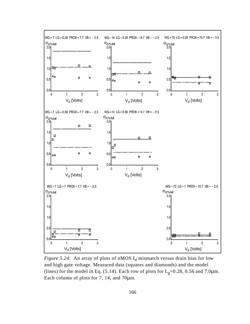
l
Figure 5.24: An array of plots of nMOS Id mismatch versus drain bias for lowand high gate voltage. Measured data (squares and diamonds) and the mode(lines) for the model in Eq. (5.14). Each row of plots for Lg=0.28, 0.56 and 7.0µm.Each column of plots for 7, 14, and 70µm.σ∆%Id σ∆%Id σ∆%Id
σ∆%Id σ∆%Id
σ∆%Id σ∆%Id
Vd [Volts] Vd [Volts] Vd [Volts]
Vd [Volts] Vd [Volts]
Vd [Volts] Vd [Volts]
166

) for
Figure 5.25: An array of plots of Id mismatch versus Vd for the nMOS devicewith Wg=7µm for measured data (squares and diamonds) and the model (linesthe model in Eq. (5.14). Each column of plots is given for Lg=0.28, 0.56, and 7µm.Each row is given for Vb=0,-1.25, -2.5V.σ∆%Id σ∆%Id σ∆%Id
σ∆%Id σ∆%Id σ∆%Id
σ∆%Id σ∆%Id σ∆%Id
Vd [Volts] Vd [Volts] Vd [Volts]
Vd [Volts] Vd [Volts] Vd [Volts]
Vd [Volts]Vd [Volts]Vd [Volts]
167
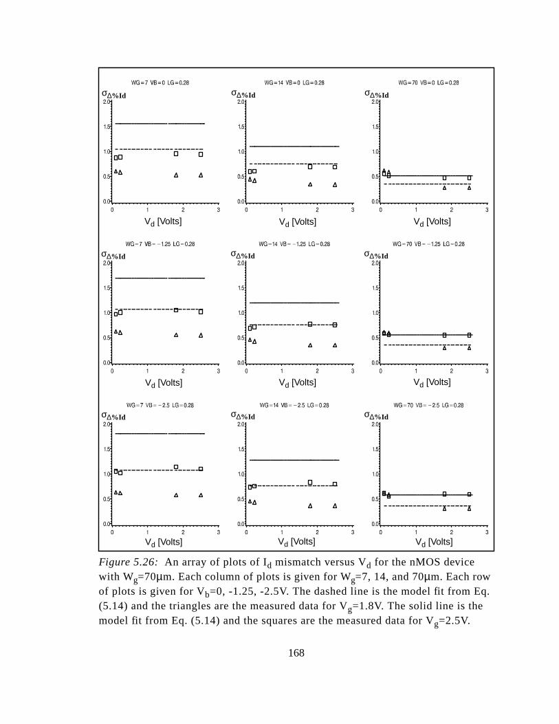
q.
Figure 5.26: An array of plots of Id mismatch versus Vd for the nMOS devicewith Wg=70µm. Each column of plots is given for Wg=7, 14, and 70µm. Each rowof plots is given for Vb=0, -1.25, -2.5V. The dashed line is the model fit from E(5.14) and the triangles are the measured data for Vg=1.8V. The solid line is themodel fit from Eq. (5.14) and the squares are the measured data for Vg=2.5V.
σ∆%Id σ∆%Id σ∆%Id
σ∆%Id σ∆%Id σ∆%Id
σ∆%Id σ∆%Id σ∆%Id
Vd [Volts] Vd [Volts] Vd [Volts]
Vd [Volts] Vd [Volts] Vd [Volts]
Vd [Volts]Vd [Volts]Vd [Volts]
168

s..
Figure 5.27: An array of plots of Id mismatch versus Vd for the largest geometrydevice(Wg=70µm, Lg=7µm) for the nMOS device. Each column of plots is givenfor minimum separation distance, and separations in two orthogonal directionEach row is given for Vb=0, -1.25, -2.5V. The dashed line is the model fit from Eq(5.14) and the triangles are the measured data for Vg=1.8V. The solid line is themodel fit from Eq. (5.14) and the squares are the measured data for Vg=2.5V
σ∆%Id σ∆%Id σ∆%Id
σ∆%Id σ∆%Id σ∆%Id
σ∆%Id σ∆%Id σ∆%Id
Vd [Volts] Vd [Volts] Vd [Volts]
Vd [Volts]Vd [Volts]Vd [Volts]
Vd [Volts] Vd [Volts] Vd [Volts]
169
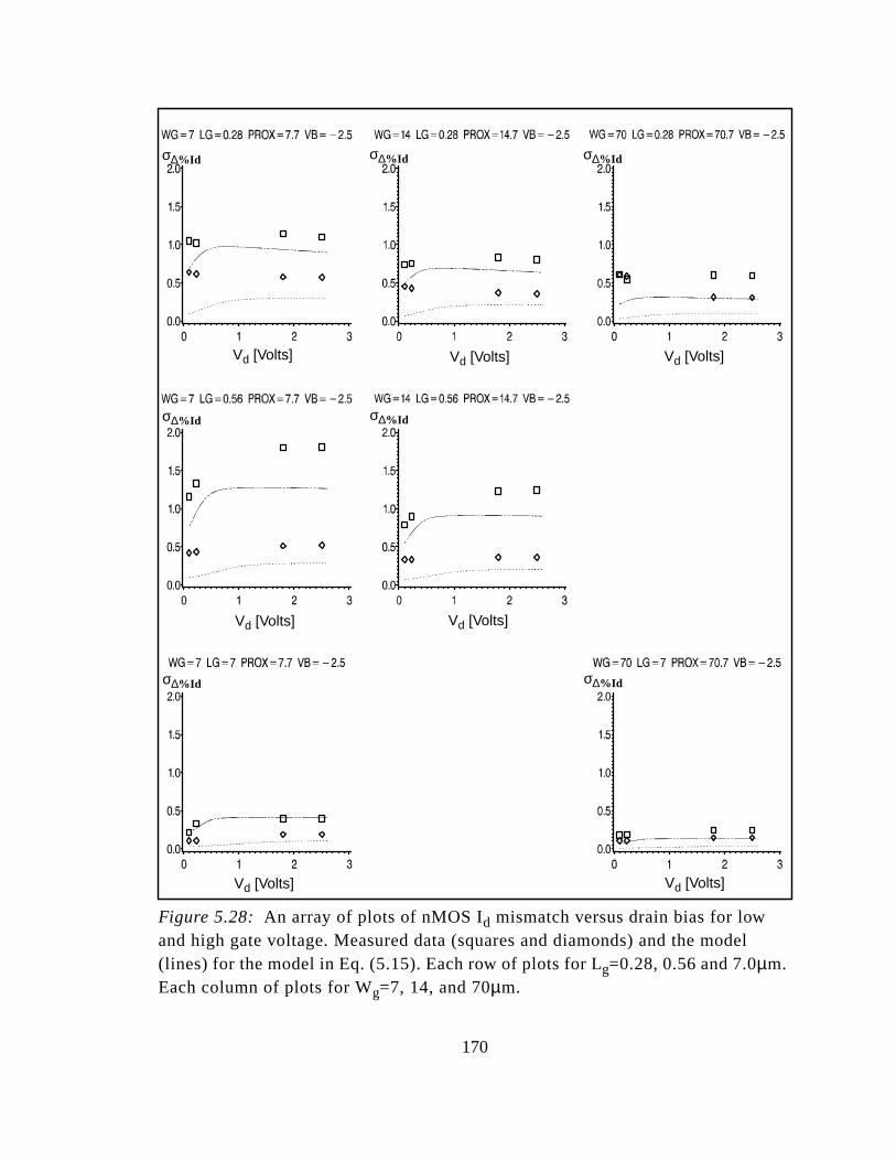
l
Figure 5.28: An array of plots of nMOS Id mismatch versus drain bias for lowand high gate voltage. Measured data (squares and diamonds) and the mode(lines) for the model in Eq. (5.15). Each row of plots for Lg=0.28, 0.56 and 7.0µm.Each column of plots for Wg=7, 14, and 70µm.σ∆%Id σ∆%Id σ∆%Id
σ∆%Id σ∆%Id
σ∆%Id σ∆%Id
Vd [Volts] Vd [Volts] Vd [Volts]
Vd [Volts] Vd [Volts]
Vd [Volts] Vd [Volts]
170

) for
Figure 5.29: An array of plots of Id mismatch versus Vd for the nMOS devicewith Wg=7µm for measured data (squares and diamonds) and the model (linesthe model in Eq. (5.15). Each column of plots is given for Lg=0.28, 0.56, and 7µm.Each row is given for Vb=0,-1.25, -2.5V.σ∆%Id σ∆%Id σ∆%Id
σ∆%Id σ∆%Id σ∆%Id
σ∆%Id σ∆%Id σ∆%Id
Vd [Volts] Vd [Volts] Vd [Volts]
Vd [Volts]Vd [Volts]Vd [Volts]
Vd [Volts] Vd [Volts] Vd [Volts]
171
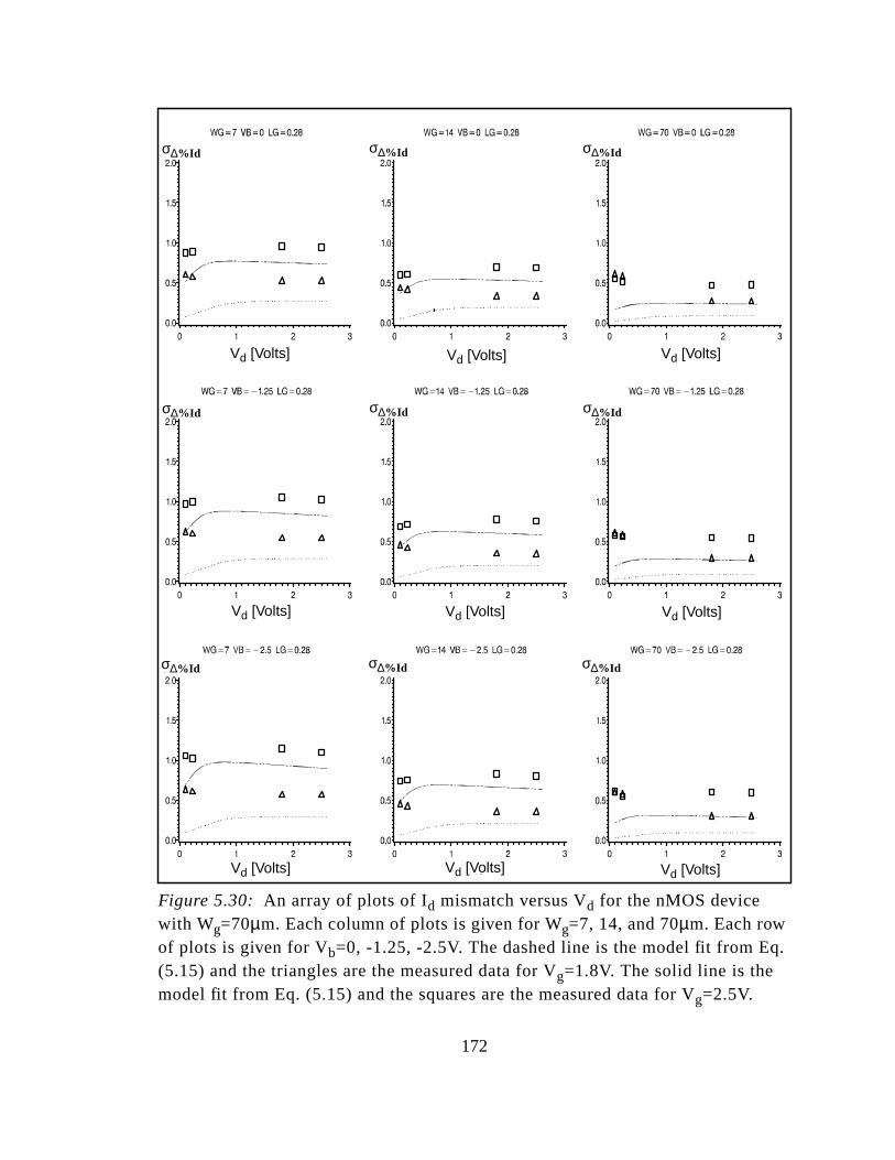
q.
Figure 5.30: An array of plots of Id mismatch versus Vd for the nMOS devicewith Wg=70µm. Each column of plots is given for Wg=7, 14, and 70µm. Each rowof plots is given for Vb=0, -1.25, -2.5V. The dashed line is the model fit from E(5.15) and the triangles are the measured data for Vg=1.8V. The solid line is themodel fit from Eq. (5.15) and the squares are the measured data for Vg=2.5V.
σ∆%Id σ∆%Id σ∆%Id
σ∆%Id σ∆%Id σ∆%Id
σ∆%Id σ∆%Id σ∆%Id
Vd [Volts] Vd [Volts] Vd [Volts]
Vd [Volts]Vd [Volts]Vd [Volts]
Vd [Volts] Vd [Volts] Vd [Volts]
172

s..
Figure 5.31: An array of plots of Id mismatch versus Vd for the largest geometrydevice(Wg=70µm, Lg=7µm) for the nMOS device. Each column of plots is givenfor minimum separation distance, and separations in two orthogonal directionEach row is given for Vb=0, -1.25, -2.5V. The dashed line is the model fit from Eq(5.15) and the triangles are the measured data for Vg=1.8V. The solid line is themodel fit from Eq. (5.15) and the squares are the measured data for Vg=2.5V
σ∆%Id σ∆%Id σ∆%Id
σ∆%Id σ∆%Id σ∆%Id
σ∆%Id σ∆%Id σ∆%Id
Vd [Volts] Vd [Volts] Vd [Volts]
Vd [Volts]Vd [Volts]Vd [Volts]
Vd [Volts] Vd [Volts] Vd [Volts]
173

l
Figure 5.32: An array of plots of nMOS Id mismatch versus drain bias for lowand high gate voltage. Measured data (squares and diamonds) and the mode(lines) for the model in Eq. (5.16). Each row of plots for Lg=0.28, 0.56 and 7.0µm.Each column of plots for 7, 14, and 70µm.σ∆%Id σ∆%Id σ∆%Id
σ∆%Id σ∆%Id
σ∆%Id σ∆%Id
Vd [Volts] Vd [Volts] Vd [Volts]
Vd [Volts] Vd [Volts]
Vd [Volts] Vd [Volts]
174
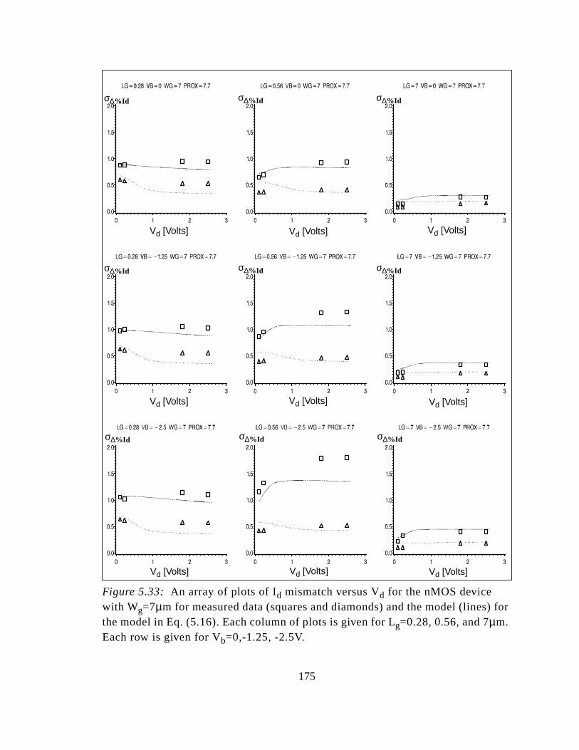
) for
Figure 5.33: An array of plots of Id mismatch versus Vd for the nMOS devicewith Wg=7µm for measured data (squares and diamonds) and the model (linesthe model in Eq. (5.16). Each column of plots is given for Lg=0.28, 0.56, and 7µm.Each row is given for Vb=0,-1.25, -2.5V.σ∆%Id σ∆%Id σ∆%Id
σ∆%Id σ∆%Id σ∆%Id
σ∆%Id σ∆%Id σ∆%Id
Vd [Volts] Vd [Volts] Vd [Volts]
Vd [Volts]Vd [Volts]Vd [Volts]
Vd [Volts] Vd [Volts] Vd [Volts]
175

q.
Figure 5.34: An array of plots of Id mismatch versus Vd for the nMOS devicewith Wg=70µm. Each column of plots is given for Wg=7, 14, and 70µm. Each rowof plots is given for Vb=0, -1.25, -2.5V. The dashed line is the model fit from E(5.16) and the triangles are the measured data for Vg=1.8V. The solid line is themodel fit from Eq. (5.16) and the squares are the measured data for Vg=2.5V.
σ∆%Id σ∆%Id σ∆%Id
σ∆%Id σ∆%Id σ∆%Id
σ∆%Id σ∆%Id σ∆%Id
Vd [Volts] Vd [Volts] Vd [Volts]
Vd [Volts]Vd [Volts]Vd [Volts]
Vd [Volts] Vd [Volts] Vd [Volts]
176

s..
Figure 5.35: An array of plots of Id mismatch versus Vd for the largest geometrydevice(Wg=70µm, Lg=7µm) for the nMOS device. Each column of plots is givenfor minimum separation distance, and separations in two orthogonal directionEach row is given for Vb=0, -1.25, -2.5V. The dashed line is the model fit from Eq(5.16) and the triangles are the measured data for Vg=1.8V. The solid line is themodel fit from Eq. (5.16) and the squares are the measured data for Vg=2.5V
σ∆%Id σ∆%Id σ∆%Id
σ∆%Id σ∆%Id σ∆%Id
σ∆%Id σ∆%Id σ∆%Id
Vd [Volts] Vd [Volts] Vd [Volts]
Vd [Volts]Vd [Volts]Vd [Volts]
Vd [Volts] Vd [Volts] Vd [Volts]
177
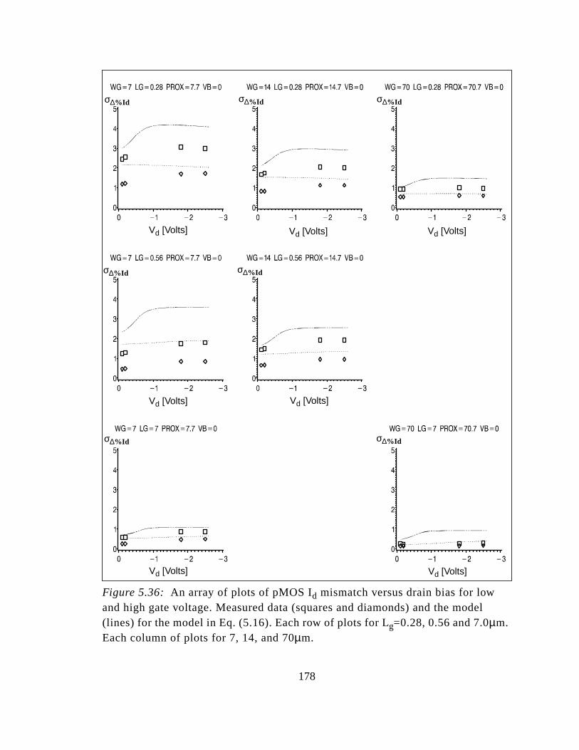
l
Figure 5.36: An array of plots of pMOS Id mismatch versus drain bias for lowand high gate voltage. Measured data (squares and diamonds) and the mode(lines) for the model in Eq. (5.16). Each row of plots for Lg=0.28, 0.56 and 7.0µm.Each column of plots for 7, 14, and 70µm.σ∆%Id σ∆%Id σ∆%Id
σ∆%Id σ∆%Id
σ∆%Id σ∆%Id
Vd [Volts] Vd [Volts] Vd [Volts]
Vd [Volts] Vd [Volts]
Vd [Volts] Vd [Volts]
178
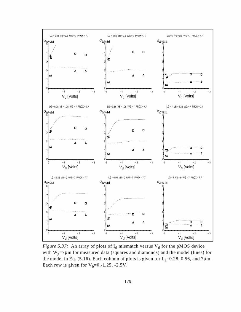
) for
Figure 5.37: An array of plots of Id mismatch versus Vd for the pMOS devicewith Wg=7µm for measured data (squares and diamonds) and the model (linesthe model in Eq. (5.16). Each column of plots is given for Lg=0.28, 0.56, and 7µm.Each row is given for Vb=0,-1.25, -2.5V.σ∆%Id σ∆%Id σ∆%Id
σ∆%Id σ∆%Id σ∆%Id
σ∆%Id σ∆%Id σ∆%Id
Vd [Volts] Vd [Volts] Vd [Volts]
Vd [Volts]Vd [Volts]Vd [Volts]
Vd [Volts] Vd [Volts] Vd [Volts]
179

q.
Figure 5.38: An array of plots of Id mismatch versus Vd for the pMOS devicewith Wg=70µm. Each column of plots is given for Wg=7, 14, and 70µm. Each rowof plots is given for Vb=0, -1.25, -2.5V. The dashed line is the model fit from E(5.16) and the triangles are the measured data for Vg=1.8V. The solid line is themodel fit from Eq. (5.16) and the squares are the measured data for Vg=2.5V.
σ∆%Id σ∆%Id σ∆%Id
σ∆%Id σ∆%Id σ∆%Id
σ∆%Id σ∆%Id σ∆%Id
Vd [Volts] Vd [Volts] Vd [Volts]
Vd [Volts]Vd [Volts]Vd [Volts]
Vd [Volts] Vd [Volts] Vd [Volts]
180

s..
Figure 5.39: An array of plots of Id mismatch versus Vd for the largest geometrydevice(Wg=70µm, Lg=7µm) for the pMOS device. Each column of plots is givenfor minimum separation distance, and separations in two orthogonal directionEach row is given for Vb=0, -1.25, -2.5V. The dashed line is the model fit from Eq(5.16) and the triangles are the measured data for Vg=1.8V. The solid line is themodel fit from Eq. (5.16) and the squares are the measured data for Vg=2.5V
σ∆%Id σ∆%Id σ∆%Id
σ∆%Id σ∆%Id σ∆%Id
σ∆%Id σ∆%Id σ∆%Id
Vd [Volts] Vd [Volts] Vd [Volts]
Vd [Volts]Vd [Volts]Vd [Volts]
Vd [Volts] Vd [Volts] Vd [Volts]
181

h
the
ina-
he
he
is-
Figure 5.40: Two plots Individual Vt mismatch measurements versus mismatcmeasurements for the nMOS device (a) and the pMOS device (b).
5.5 Experimental design for mismatch pairs
One of the most important aspects to the solution of Eq. (5.9) is rank of
sensitivity matrix. It is paramount to the BPV technique to have enough comb
tions of Id mismatch measurements across the geometry and bias space for t
individual process and geometry mismatch variances to be sufficiently and
uniquely visible. For instance, a narrow MOSFET and a wide MOSFET are
needed to determine the contribution of the mismatch. Likewise, across t
bias conditions, a Id mismatch value for Vgs slightly above Vt will is most sensi-
tive to the Vt process parameters listed in Eq. (5.9). More elaborate electrical m
match parameters such as gm mismatch or Vt mismatch can be used in lieu of Id
DVTO
-20.00
-15.00
-10.00
-5.00
0.00
5.00
10.00
15.00
20.00
DGMMAX-8 -6 -4 -2 0 2 4 6
DVTO
-20.00
-15.00
-10.00
-5.00
0.00
5.00
10.00
15.00
20.00
DGMMAX-8 -6 -4 -2 0 2 4 6
Vt mismatchVt mismatch
β mismatchβ mismatch
(a) (b)
β
∆W
182

ess
tion
ike-
atch
ugh-
D-
ndi-
s
n
of
n
ble
mismatch but they do not add any value to the extraction since all of the proc
and geometry parameters are uniquely visible in Id mismatch for the right bias and
geometry combinations.
There is a strong desire to derive a minimum set mismatch characteriza
test structures since the area available on a test mask is often fairly limited. L
wise, the bias conditions should be minimized so as the glean the most mism
information from the fewest measurement, thereby improving equipment thro
put and capital utilization. A alphabetic-optimal experimental design (e.g. the
optimal design) is a good candidate to derive the set of bias and geometry co
tions that should be used to characterized MOS mismatch.
The D-optimal design strives to minimize the variance of the prediction
resulting from the fit of Eq. (5.9). Taking the general form of Eq. (5.9) in Eq.
(3.22) prediction variance from the least squares solution is,
(5.17)
where the positive definite square matrix, is known as the informatio
matrix. The D-optimal design is targeted towards maximizing the determinant
the information matrix which is equivalent to finding the best over-all predictio
variance over the design space. Other alphabetic optimality criteria are possi
Var Ψ( ) σ2 Λ2( )'Λ2( )1–
=
Λ2( )'Λ2( )
183

hich
l
wo
ent
to
lues
el
n
can
ol-
or
vice
ters
ty to
alternatives such as the A-optimal design and the G-optimal design. The A-
optimal design minimizes the variances of the model parameter estimates, w
in this case is the process and geometry mismatch variances.
There are two problems associated with choosing an alphabetic optima
design. The poor condition of the information matrix means that only one or t
of the parameters will dominate the solution. In conventional design of experim
theory, the condition is controlled by normalizing the independent parameters
scale between values of -1 and +1. It is practically impossible to scale the va
of the sensitivity matrix, given the complex and highly non-linear SPICE mod
contained within the sensitivity matrix.
In addition, the SPICE model is subject to change considerably betwee
different MOSFET types. An optimal design for an nMOS on one technology
be completely different than the design for another nMOS in a separate techn
ogy. It is impractical to change the condition for the treatment combinations f
many technologies. Instead, the experimental design is approach from the de
physics side of the problem.
The design of the experiment to extract the MOSFET mismatch parame
begins with an evaluation of the conditions for maximum sensitivity of Id mis-
match to each parameter. Each parameter is evaluated in terms of its sensitivi
both the small signal variation and the gradient effect contributions.
184

-
d
n-
s.
on
5.5.1 mismatch
• Small Signal Variation -Desire minimum Wg to maximize the impact of
on Id mismatch. Desire minimum Lg to maximize (Lg) since improves
asymptotically with increasing Lg. Bias conditions are arbitrary.
• Gradient Effect - Desire minimum Wg to maximize the impact of on
Id mismatch. Desire a large Lg to minimize the contribution from the small
signal variation in and other process parameters.
5.5.2 mismatch
• Small Signal Variation - Desireminimum Lg and minimum Wg. Combine
nMOS and pMOS fits to uniquely extract the variation from the varia
tion. Id mismatch is most sensitive to variation for Vg slightly above the
threshold voltage through the Vt mismatch. mismatch impact is also increase
for maximum Vb through the body effect.
• Gradient Effect - Desire large length and large width to minimize the co
tributions from the small signal variation and other mismatch source
Similarly extracted from the simultaneous fit of the nMOS and pMOS
devices. Also uses the same bias conditions as the small signal variati
treatment combination.
∆W
∆W
∆W ∆W
∆W
∆W
tox
tox Nsub
tox
tox
tox
185

he
ra-
verse
ct
deter-
rma-
5.5.3 mismatch
• Small Signal Variation -Desire minimum Lg and minimum Wg since the small
signal variation decreases with increasing gate area. Need Vg slightly above Vt
since the impact of on Id mismatch decreases with increasing overdrive on t
gate. Vd is arbitrary since the effect of is observable in the linear and satu
tion regions. Vb = 0 to avoid conflicting contributions from and through
the body effect. Additional geometries to detect non-monotonicities in the Id mis-
match over geometry due to the short channel effect as in Figure 5.14, the re
short channel effect, the narrow width effect and the inverse narrow width effe
are not required since the location and extent of these effects will have been
mined a priori and modeled in the SPICE model file (provided the model can
include these effects). The added geometries can provide experimental confi
tion of the phenomena, however.
• Gradient Effect - Desire large Lg and large Wg to minimize the contribu-
tion of the small signal variation of on Id mismatch.Bias conditions are
the same as for the small signal variation.
5.5.4 mismatch
• Small Signal Variation -Desire minimum Lg and minimum Wg since the small
signal variation decreases with increasing gate area. Need maximum Vg since the
V fb
V fb
V fb
tox Nsub
V fb
µo
186

all
.
L
impact of the Vt mismatch sources on Id mismatch decrease with increasing gate
overdrive. Vd is somewhat arbitrary but prefer to set Vd = 0.1 to avoid other con-
founding effects such as velocity saturation and DIBL. Vb is arbitrary.
• Gradient Effect - Desire large Lg and large Wg to minimize the impact of
the small signal variation of . USe the same bias conditions as the sm
signal variation case.
5.5.5 mismatch
• Small Signal Variation - Desireminimum Lg to maximize the impact of
on Id mismatch. Desire minimum Wg to maximize (Wg) since improves
asymptotically with increasing Wg. Bias conditions are arbitrary.
• Gradient Effect - Desireminimum Lg to maximize the impact of on Id
mismatch. Large Wg to minimize the contribution from the small signal variation
Bias conditions are arbitrary.
5.5.6 mismatch
• Small Signal Variation - Need two device geometries. Need minimumg
to maximize the sensitivity and a longer Lg to observe the short channel
effect. Wg is arbitrary since variance decreases with increasing Wg.
Need Vg slightly above Vt, Vb=0 to minimize the contributions from
µo
∆L
∆L
∆L ∆L
∆L
Vtl
Vtl
tox
187

ria-
annel
-
ut
-
ith
tend-
er lit-
teral
and variation to the threshold voltage mismatch through the body
effect. Vd is arbitrary.
• Gradient Effect - Need Same bias conditions as for the small signal va
tion case but with a large separation distance.
5.5.7 mismatch
• Small Signal Variation - Desire minimum Lg to maximize the impact of
on the Id mismatch variance. Wg is somewhat arbitrary since both the
series resistance and the channel resistance scale together with the ch
width. mismatch variation improves with increasing Wg but so does the
channel resistance. Wg should be set to a large value to minimize the con
tribution from other mismatch sources. Desire maximum Vg to minimize
the contribution from the intrinsic channel resistance to the overall outp
resistance. Desire Vd = 0.1V to minimize the contributions from the intrin
sic MOSFET mismatch sources. Vb is somewhat arbitrary.
• Gradient Effect -Same conditions as for the small signal variation case but w
a large separation distance between the two devices in the mismatch pair. Ex
ing the distance from the gate edge to the source and drain contacts would off
tle improvement since the majority of the series resistance comes from the la
out-diffusion of the source / drain areas under the gate.
Nsub
ρsh
ρsh
ρsh
188

as
ent
ble
ly a
fer-
t
y
ions
ach
5.5.8 mismatch
• Small Signal Variation - Desireminimum Lg and minimum Wg. Need a max-
imum Vb since the mismatch primarily affects the Id mismatch through the
body effect. Need a Vg slightly above threshold to maximize the Id mismatch sen-
sitivity to Vt mismatch through which the body effect is apparent. Note that Vt
increases in magnitude for an increase in Vb. Therefore the Vg must be “smart” to
adjust itself above the threshold voltage change. Vd is arbitrary.
• Gradient Effect - Desire large Lg and large Wg to minimize he contribu-
tion from the small signal mismatch. Bias conditions are the same
for the small signal variation case.
Compiling the treatment combinations for the eight process parameters
results in the set of devices listed in Table 5.18. A separate list of measurem
treatment combinations is given in Table 5.19. The list of measurements in Ta
5.19 was separated from the list of device geometries since it is easier to app
single mismatch measurement algorithm to all devices rather than apply a dif
ent set of biases to each geometry. In addition, given the limited space on tes
masks and process monitoring pad arrays, it is expensive to add unnecessar
device geometries, while the cost associated for adding additional bias condit
is often cheaper, particularly in the characterization environment. Therefore, e
Nsub
Nsub
Nsub
189

s
for
to
9 is
.
.19
of the bias combinations listed in Table 5.19 are applied to each of the device
listed in Table 5.18.
Table 5.18: A minimum list of device geometry treatment combinations (tc’s) the MOSFET experimental design.
Table 5.19: A minimum list of measurement condition treatment combinationsbe applied to each of the MOSFETs listed in Table 5.18.MOSFET mismatch pairis placed in a common source configuration.
The minimum experimental design prescribed Table 5.18 and Table 5.1
not unlike the original design of experiment (DOE) proposed in Section 3.7.2
Essentially the DOE in Section 3.7.2 is a super-set of Table 5.18 and Table 5
tc Gate Length Gate Width Proximity Parameters Covered
1 minimum minimum minimum , , , , , , ,
2 minimum large large ,
3 large minimum large
4 large large large , , ,
5 minimum large minimum
tc Vd (V) Vg (V) Vb (V) Parameters Covered
1 0.1 maximum 0 , , , ,
2 0.1 >Vt 0 , , ,
3 0.1 >Vt max ,
∆W tox V fb µo ∆L Vtl ρsh
Nsub
∆L ρsh
∆W
tox V fb µo Nsub
ρsh
∆W µo ∆L ρsh
tox V fb Vtl
tox Nsub
190

the
with additional intermediate bias and geometry points to allow observation oftrends.
191

ble
an-
ct-
s
pant
h is
r-
ed as
Chapter 6 BJT Mismatch
6.1 Prior work
Despite the proliferation of MOSFETs and CMOS-only processes in the
semiconductor world, bipolar and BiCMOS processes have maintained a siza
market. In addition to some useful gain and temperature properties, bipolar tr
sistors tend to have better mismatch performance than MOSFETs.
The foundation of BJT mismatch comes from Gray and Meyer [5]. Negle
ing offset and setting , analysis of a BJT current mirror pair give
a collector current ratio
(6.1)
where the subscripts and denote the two transistors in the mirror,
is emitter area, the electron diffusion constant in the base, the base do
concentration profile, and the base width. Eq. (6.1) shows that mismatc
physically caused by mismatches in , , and , all of which have a
dependence.
Connor and Evanson [66] proposed a differential amplifier circuit to cha
acterize BJT and resistor mismatch. The base inputs to a differential pair of
matched bipolar transistors were tied together as the input. Resistors were us
I b Vbe1 Vbe2=
I c1
I c2-------
I S1
I S2-------
A1 De2 x( )NA2
x( ) xdWB2
∫A2 De1 x( )N
A1x( ) xd
WB1∫
---------------------------------------------------------------= =
1 2 A LeWe=
De NA
WB I c
A NA WB
1 LeWe( )⁄
192

on
r the
t of
this
t
ch.
s
.
ea-
par-
se
s
r
try
el-
E
passive loads. The mismatch was measured as the differential output voltage
the collector nodes. Since the output offset voltage can be produced by eithe
BJTs or the resistors, Darlington pair switches were used to flip the assignmen
the resistor loads to each BJT, thereby orthogonalizing the effects. Not only is
approach complicated but it is only capable of measuring the collector curren
mismatch.
Tuinhout and Peters [59] and Tuinhout [11] proposed a simpler approa
Here, an explicit BJT matched pair is placed in a common collector, common
emitter configuration as depict in Figure 6.1. Although this test structure save
one pad versus a common emitter configuration, it has a fundamental problem
Both devices must be biased at the same time. While the first device is being m
sured, leakage current contributions from the second device will be measured,
ticularly for high frequency, narrow base devices with low BVCEO values. The
confounded measurements will be most apparent for low Vbe measurements,
where the mismatch will be underestimated since current from both devices i
measured. Tuinhout used the Pelgrom model (mismatch variance = 1/(emitte
area)) to fit the collector current with reasonable success although the geome
selection was conducive to the fit.
A model such as Eq. (3.52), which is more general adaptation of the P
grom model, can be used for BJT mismatch based on parameters of the SPIC
193

ed
del
en
that
.
e
Gummel-Poon (SGP) model. Mismatch data for and are measur
for matched pairs, and the parameters in the model
(6.2)
are extracted to fit the measured variances ( is the spacing between device
emitter centers). The and terms allow for independent perimeter
mismatches. The model Eq. (6.2) is then directly implemented via the SGP mo
parameters and . However, this does not account for correlations betwe
model parameters like the ones in Eq. (6.1). Figure 6.2 and Figure 6.3 show
this can lead to inaccurate modeling of mismatch over bias and geometry. In
Figure 6.2, in the high current region, mismatch increases as increases
However, the model predicts a decrease in mismatch as increases since th
mismatch in does not model this. Likewise in Figure 6.3, the increase in
mismatch in the low level injection region is not modeled.
I c β I c I b⁄=
σi
σI cMM βMM,2 σLW
2
WeLe--------------
σW2
We2
--------σL
2
Le2
------ d2S
2+ + +=
S
1 Le2⁄ 1 We
2⁄
I S BF
I c I c
I c
I S β
194
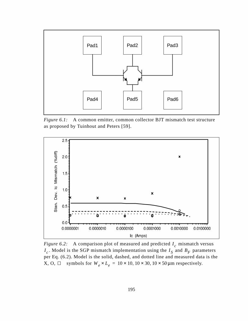
e
serss the
Figure 6.1: A common emitter, common collector BJT mismatch test structuras proposed by Tuinhout and Peters [59].
Figure 6.2: A comparison plot of measured and predicted mismatch versu. Model is the SGP mismatch implementation using the and paramet
per Eq. (6.2). Model is the solid, dashed, and dotted line and measured data iX, O, symbols for µm respectively.
Pad1 Pad2
Pad4 Pad5
Pad3
Pad6
O OOOOOO OOOOOO OOOOOO
OOOOOO
I cI c I S BF
We Le× 10 10× 10 30× 10 50×, ,=
195
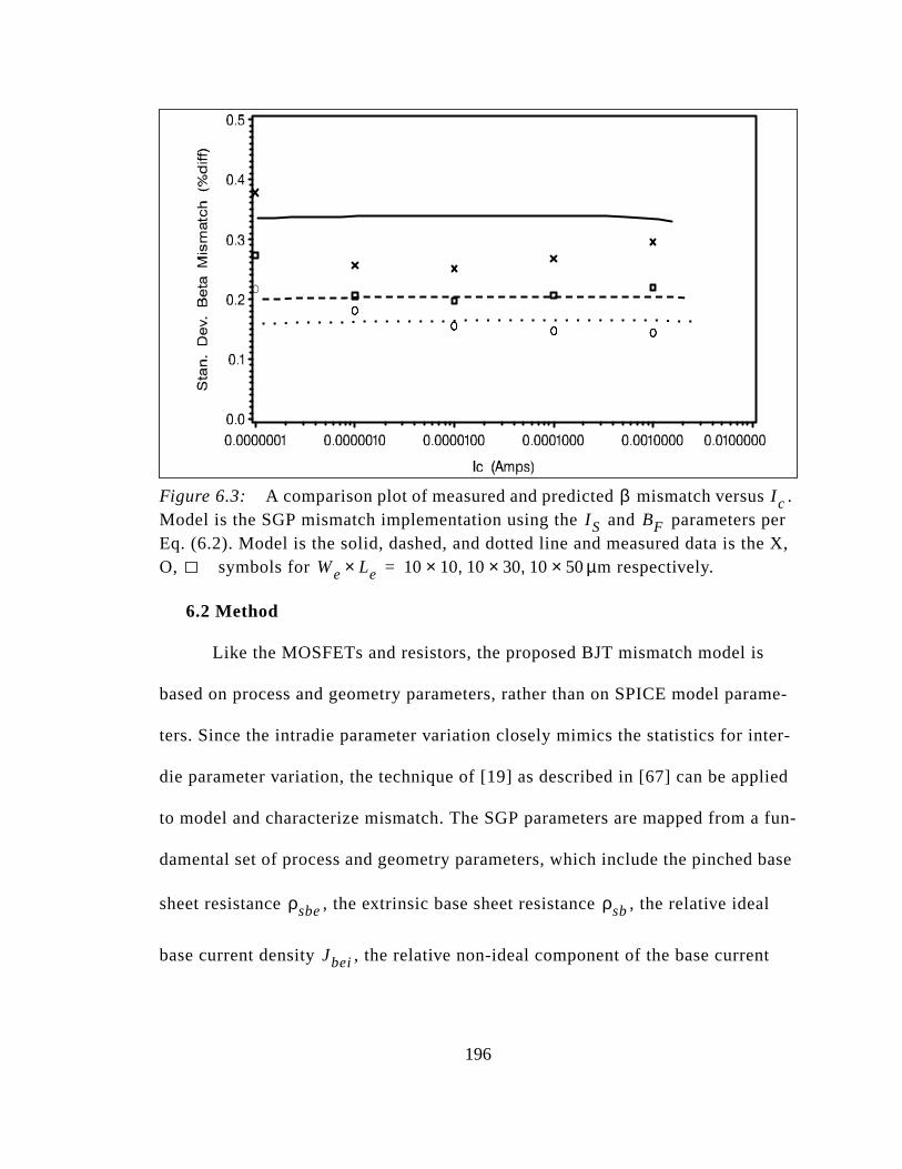
.pere X,
rame-
ter-
lied
a fun-
base
al
nt
Figure 6.3: A comparison plot of measured and predicted mismatch versusModel is the SGP mismatch implementation using the and parameters Eq. (6.2). Model is the solid, dashed, and dotted line and measured data is thO, symbols for µm respectively.
6.2 Method
Like the MOSFETs and resistors, the proposed BJT mismatch model is
based on process and geometry parameters, rather than on SPICE model pa
ters. Since the intradie parameter variation closely mimics the statistics for in
die parameter variation, the technique of [19] as described in [67] can be app
to model and characterize mismatch. The SGP parameters are mapped from
damental set of process and geometry parameters, which include the pinched
sheet resistance , the extrinsic base sheet resistance , the relative ide
base current density , the relative non-ideal component of the base curre
O
OOOOOOOOOOOO OOOOOO OOOOOO
β I cI S BF
We Le× 10 10× 10 30× 10 50×, ,=
ρsbe ρsb
Jbei
196

s in
ing
into
rame-
del
ed
s are
, ,
mis-
, and geometric deviations in the emitter length and width . Unlike the
MOSFETs, only a single geometric parameter is used for mismatch deviation
length and width since both dimensions are determined by the same process
step. These are nearly independent, physical parameters that, when mapped
the SGP model parameters, account for the correlations between the SGP pa
ters. The key to this approach is availability of a scalable, statistical SGP mo
(see Davis and Ida [68]).
Mismatch data is collected for , , and over geometries as specifi
by the experimental design in Section 3.7.2, and many biases. Measurement
needed for all three electrical parameters. Using a fitted SGP model with the
appropriate process and geometry parameter mappings, the sensitivities of
and with respect to process parameters were calculated from SPICE. The
match model is,
Jben ∆
I c I b β
I c I b
β
197

was
rs
in a
ble
,
le
nta-
(6.3)
Eq. (6.3) can be solved using linear regression, however, nonlinear regression
used to placed positive value boundaries on the process parameters.
6.3 A vertical NPN from a 0.8µm BiCMOS technology.
6.3.1 Process conditions and measurements
A diffused vertical NPN in a 0.8µm power BiCMOS technology was mea-
sured for mismatch using the scheme describes in Section 6.2. Mismatch pai
geometries are listed in Table 6.1. Mismatch measurements were performed
common emitter configuration. Bias and temperature conditions are listed in Ta
6.2. , and mismatch data were collected for all combinations of ,
temperature and geometry. Data were collected from 16 die sites from a sing
wafer. Previous studies from a similar technology showed this to be a represe
tive sample.
σIcmm2
σIbmm2
σBtmm2
…
∆d
dIc
2
psbed
dIc
2
psbd
dIc
2
j beid
dIc
2
j bend
dIc
2
ncold
dIc
2
∆d
dIb
2
psbed
dIb
2
psbd
dIb
2
j beid
dIb
2
j bend
dIb
2
ncold
dIb
2
∆dd
B 2
psbedd
B 2
psbdd
B 2
j beid
dB
2
j bend
dB
2
ncoldd
B 2
… … … … … …
σδ∆2
σ psbe
2
σ psb
2
σj bei
2
σj ben
2
σncol
2
=
I c I b β I c Vce
198

Table 6.1: Geometry treatment combinations(tc) for the bipolar transistormismatch test structures.
Table 6.2: Bias and temperature treatment combinations for the mismatchmeasurements.
tcEmitter
Width (µm)Emitter
Length (µm)Proximity
(µm)
1 2.4 2.4 39.8
2 2.4 4.8 42.2
3 4.8 2.4 39.8
4 4.8 4.8 42.2
5 2.4 24.0 61.4
6 24.0 2.4 39.8
7 24.0 24.0 61.4
8 24.0 24.0 500
Parameter Levels
EmitterVoltage
common emitter configuration
BaseVoltage
swept to target =0.1, 1, 10, 100, and 1000µA
CollectorVoltage
2, 5, and 15V
Temperature 27 and 100C
I c
199

ilde
del
st
ith
of
for
but
the
6.3.2 Analysis
Table 6.3 gives extracted mismatch variances for the NPN device. The t
indicates a normalized parameter.
Figure 6.4 through Figure 6.6 show playbacks of the new mismatch mo
over geometry and bias. Most notable, in the top curves and data (the smalle
geometry), is the sharp increase in and mismatch for low current levels, w
no corresponding increase in the mismatch of . The expected improvement
mismatch with increased geometry is also observed.
Table 6.3: Mismatch parameters for device A.
Figure 6.7 shows the individual contributions to the predicted mismatch
the top curve in Figure 6.6. Note that standard deviations are given in this plot,
it is the sum of variances that gives the predicted mismatch curve denoted by
Geometric scalingfactor
0.631µm 0.001
0.303 0.00173µm-1
0.0 0.0135µm-1
3.56 0.00245µm-1
60.56 0.0172µm-1
1.90 0.001µm-1
I b β
I c
b1 b2
σδ∆
σ psbe1
LeWe--------------
σ psb1Le-----
σj bei
1LeWe--------------
σj ben
1LeWe--------------
σncol1
LeWe--------------
200

is
ed
r-
tch
y
ig-
slinend 8
X’s. From Figure 6.7 it is apparent that the mismatch in in the ideal region
dominated by mismatch, with a small contribution from . As the match
pair is biased into the low current region, the mismatch in becomes impo
tant and eventually dominates the mismatch. Since only the and misma
are affected by the mismatch in and , the mismatch is qualitativel
different. In fact, the mismatch in Figure 6.4 tracks the mismatch in F
ure 6.7, as expected physically at low .
Figure 6.4: A comparison plot of measured and predicted mismatch versu. Model is implemented as Eq. (6.3). Model is the solid, dashed, and dotted
and measured data is the X, O, symbols for geometries listed as tc 1, 4, arespectively.
β
Jbei ρsbe
Jben
β β I b
Jbei Jben I c
I c ρsbe
I c
O O O O O
Outlier
I cI c
201
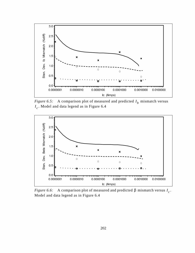
s
.
Figure 6.5: A comparison plot of measured and predicted mismatch versu. Model and data legend as in Figure 6.4
Figure 6.6: A comparison plot of measured and predicted mismatch versusModel and data legend as in Figure 6.4
O
OO
O
O
I bI c
O
OO O O
β I c
202

ility
ec-
tch
by
base
Figure 6.7: Components plot of mismatch versus . Symbol 1= , 2= ,3= , 4= , 5= , and X=total (rms) mismatch.
6.3.3 Geometric scaling
Figure 6.8, Figure 6.9, and Figure 6.10 demonstrate the scaling capab
of the new mismatch model. Figure 6.8 shows the , , and mismatch for
three different emitter lengths for a minimum emitter width. As discussed in S
tion 6.3.2, the and mismatch closely mimic each other due to the misma
contributions from and .
In the bottom row of plots in Figure 6.9, the and mismatch slightly
increases for large emitter widths and high collector currents. This is caused
the relative increase in base resistance from the extrinsic base as the intrinsic
becomes conductivity modulated.
1 1 1 1 1 1 1 1 1 1 1 1 1 1 1 1 1 1 1 1 1 1 1
12 2 2 2 2 2 2 2 2 2 2 2 2 2 2 2 2 2 2 2 2 2 223 3 3 3 3 3 3 3 3 3 3 3 3 3 3 3 3 3 3 3 3 3 3
3
4 4 4 4 4 4 4 4 4 4 4 4 4 4 4 4 4 4 4 4 4 44
4
5
5
5
555555 5 5 5 5 5 5 5 5 5 5 5 5 5 556 6 6 6 6 6 6 6 6 6 6 6 6 6 6 6 6 6 6 6 6 6 6
6
β I c ∆ ρsbeρsb Jbei Jben
β I b I c
β I b
Jbei Jben
β I b
203

me-
only
-
geo-
ice
n
Figure 6.10 shows a smooth monotonic trend in the mismatch over geo
try for .
The mismatch standard deviation is commonly modeled as depending
on the inverse square root area, but Eq. (6.2) includes other compo
nents. Per the discussion for resistors in Section 4.4, Figure 6.11 shows the
metric scaling of our model. Not all emitter areas are equivalent in terms of dev
mismatch. This plot shows that the new mismatch model is more accurate tha
previous approaches.
Le We=
1 LeWe⁄
204

n)tch
Figure 6.8: An array of plots of , , and mismatch (separated by columversus for three different emitter lengths (separated by row). The mismaplots are labeled with “PARAM=bt” in the heading.
β I b I cI c β
205
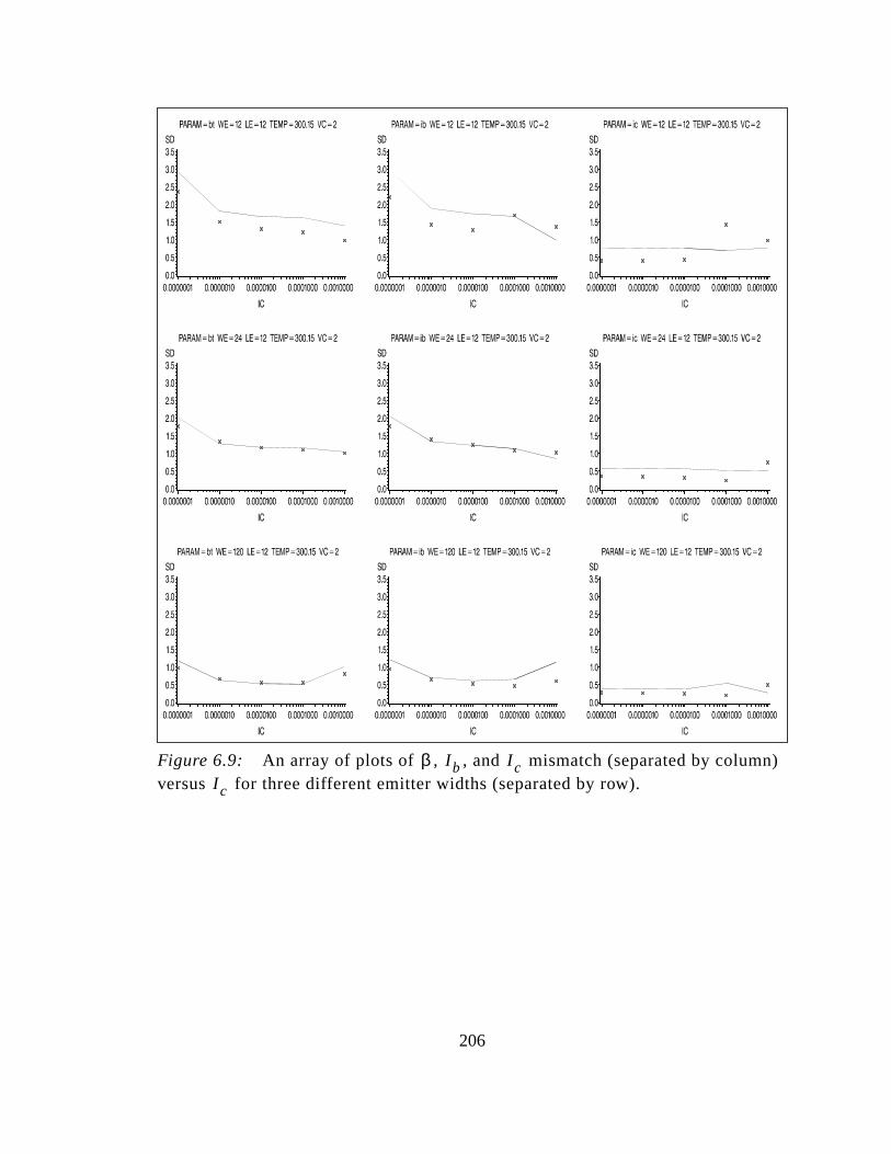
n)
Figure 6.9: An array of plots of , , and mismatch (separated by columversus for three different emitter widths (separated by row).β I b I cI c
206
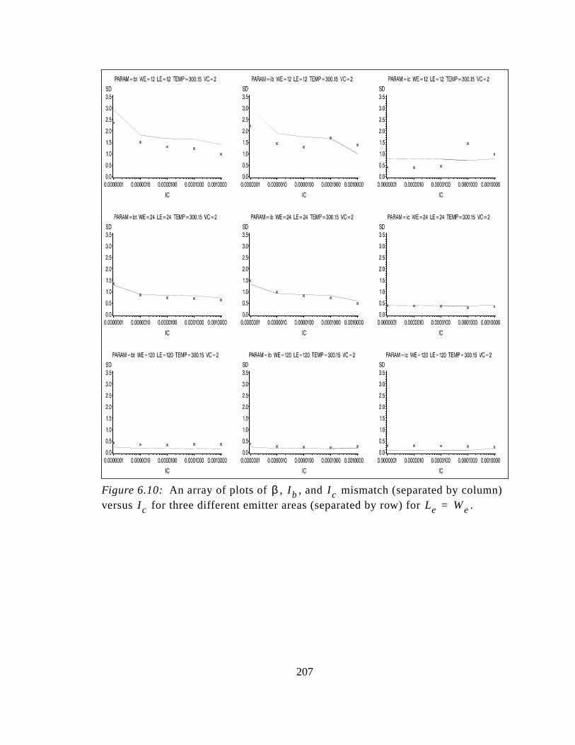
n)
Figure 6.10: An array of plots of , , and mismatch (separated by columversus for three different emitter areas (separated by row) for .β I b I cI c Le We=
207

isot-
ivity
ure
s-
is
of
Figure 6.11: An example plot of mismatch versus . Measured datagiven by X’s; the solid line: ; the dashed line: minimum ; and the dted line: minimum .
6.3.4 Temperature and Vce dependence
Figure 6.12 shows mismatch over temperature. Despite the large sensit
of BJT performance to temperature, it is clear from this plot that the temperat
has almost no impact on the BJT mismatch for any of the three measured mi
match parameters. In those instances where there is a difference, the model
qualitatively correct.
Figure 6.13 shows a representative example of mismatch over a range
biases. Again the shift is modest.
β 1 LeWe⁄Le We= Le
We
Vce
208

n)e
Figure 6.12: An array of plots of , , and mismatch (separated by columversus for three different emitter areas (separated by row) for . Thmeasured data for 27C is given by X’s and the 100C data is given by O’s. Thesolid line is model for 27C and the dashed line is model for 100C.
O
O
OO
O
O
O
O OO
O O O O O
O
O
O O
O
O
O
OO
O
O O O O O
O O O
O
O
O O O O O
O O O O O
β I b I cI c Le We=
209
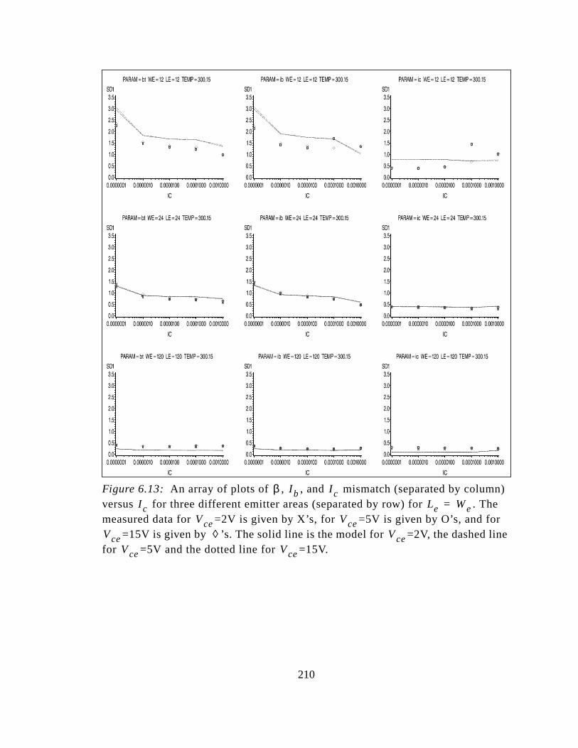
n)ere
Figure 6.13: An array of plots of , , and mismatch (separated by columversus for three different emitter areas (separated by row) for . Thmeasured data for =2V is given by X’s, for =5V is given by O’s, and fo
=15V is given by ’s. The solid line is the model for =2V, the dashed linfor =5V and the dotted line for =15V.
O
OO O
O
O
OO O O
O O O O O
O
OO
O
O
O
OO O
O
OO O O O
O O O
O
O
O O O O O
O O O O O
β I b I cI c Le We=
Vce VceVce ◊ Vce
Vce Vce
210

e-
d
-
tch
nces
air
t
ther.
ses.
6.4 A vertical NPN from a 1.8µm BiCMOS technology.
6.4.1 Process conditions and measurements
A diffused vertical NPN from a 1.76µm power BiCMOS technology was
analyzed. Emitter geometries presented were 10x10, 10x30, and 10x50µm. 20 die
sites were measured from two wafers from two lots at 27C and =2V.
6.4.2 Analysis
This BJT shows a qualitatively different variation of mismatch with bias
and geometry in Figure 6.14 through Figure 6.16 in comparison to the BJT pr
sented in Section 6.3. For this device there is no significant increase in an
mismatch for low current levels, however there is a marked increase in mis
match at high current levels. In addition, rather than the qualitative mismatch
characteristics being similar between and , and different to that of , the
mismatch characteristics of and are similar, and different to that of .
The degradation in mismatch of and at high is caused by misma
between the base and emitter resistances of the matched pair. Different resista
give rise to different intrinsic values between the devices of the matched p
at high forward bias, and hence different and values. But this should no
cause mismatch in since the resistance contributions should cancel each o
Further, as increases, the increase in and mismatch at high decrea
Vce
I b β
I c
I b β I c
I c I b β
I c I b I c
Vbe
I c I b
β
Le I c I b I c
211

are
s.
.
e
s,
, via
et-
etry
ta.
This follows because the larger devices operate at lower current densities, and
therefore less affected by the debiasing from the base and emitter resistance
The contribution plot of Figure 6.17 shows this graphically. The mis-
match is dominated by geometric variation ( ) in the ideal region of operation
The contribution plot for mismatch is similar to that of Figure 6.17, but unlik
mismatch it is not sensitive to in the low current region. At high current
mismatch becomes dominated by mismatch in the extrinsic base resistance
.
In addition, in Figure 6.17, emitter size variations affect and
strongly, but not . A device in which the dominant cause of mismatch is geom
ric variation should have large, similar mismatch behavior over bias and geom
for and , and significantly smaller mismatch for as observed in this da
I b
∆
I c
I b Jben
I b
ρsb
I c I b
β
I c I b β
212
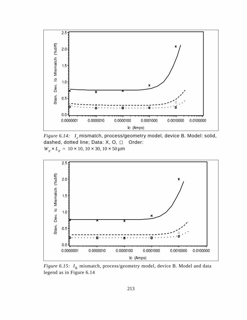
Figure 6.14: mismatch, process/geometry model, device B. Model: solid,dashed, dotted line; Data: X, O, Order:
µm
Figure 6.15: mismatch, process/geometry model, device B. Model and datalegend as in Figure 6.14
O O O OO
I c
We Le× 10 10× 10 30× 10 50×, ,=
O O O O
O
I b
213
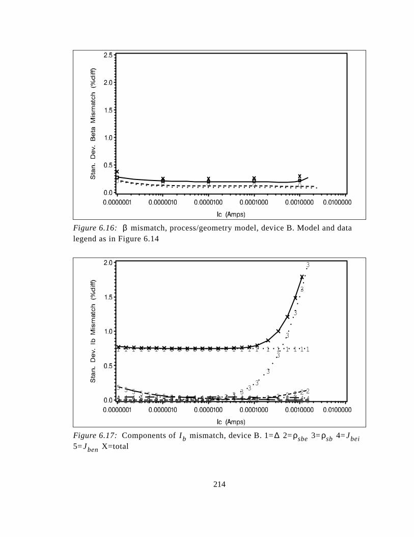
Figure 6.16: mismatch, process/geometry model, device B. Model and datalegend as in Figure 6.14
Figure 6.17: Components of mismatch, device B. 1= 2= 3= 4=5= X=total
O O O O O
β
1 1 1 1 1 1 1 1 1 1 1 1 1 1 1 1 1 1 1 1 1 1 1 1 1
2 2 2 2 2 2 2 2 2 2 2 2 2 2 2 2 2 2 2 2 2 2 2 2 23 3 3 3 3 3 3 3 3 3 3 3 3 3 3 3 3 3
3
3
3
3
3
3
3
4 4 4 4 4 4 4 4 4 4 4 4 4 4 4 4 4 4 4 4 4 4 4 4 4
5 5 5 5 5 5 5 5 5 5 5 5 5 5 5 5 5 5 5 5 5 5 5 5 5
I b ∆ ρsbe ρsb JbeiJben
214

or
ng
de-
h as
n a
r-
he
he
fset
ched-
ible
t is,
e by
Although demonstrative data is not available, there is a third scenario f
BJT mismatch where the mismatch shows an initial decrease with increasi
, before increasing. dominated mismatch will be reflected in the and
mismatch but will not be apparent for mismatch. Furthermore there is a tra
off in gain and base resistance that will create an improvement in mismatc
the current increases. Figure 6.18 depicts this phenomena. For two devices i
matched pair, one with a slightly lower intrinsic base doping, the lower doped
device will experience a larger gain. As the two devices transition to larger cu
rents, the base resistances start to play a role in the mismatch. However, t
lower doped device, which has the higher gain, will also have the higher base
resistance. This is depicted by the earlier roll-off in the high current region of t
Gummel curve in Figure 6.18. Thus the base resistance mismatch effect will of
the gain mismatch effect, both of which are caused by mismatches in the pin
base sheet resistance.
This phenomenon produces an interesting feature in that it may be poss
to improve the mismatch of such devices by decreasing the emitter area. Tha
the mismatch may be improved by increasing the current density of the devic
producing enough base resistance to offset the gain.
I c
I c ρsbe I c β
I b
I c
I c
215

isesis-
of
ng is
o the
eters
map-
s
e
sing
b
Figure 6.18: A depiction of the Gummel curves for two matched BJTs that aredominated by mismatch. For low to moderate currents, the mismatch dominated by gain mismatch but as the current increases, the intrinsic base rtance will offset the gain mismatch, thereby decreasing the mismatch.
6.5 Rapid evaluation of BJT mismatch
The plot in Figure 6.19 gives a conceptual description of the influence
the process parameters to the Gummel curves of a BJT. The parameter mappi
rearranged in Figure 6.20 to demonstrate the unique mapping of parameters t
electrical parameter space. The mappings of the three primary process param
in the ideal region are given in Figure 6.20(a), (b), and (c). From these three
pings, there is an opportunity to very quickly determine the underlying proces
parameter that is causing the mismatch. That is, if the Ic mismatch mimics th
mismatch, as in Figure 6.20(a), must be the process parameter that is cau
the mismatch. Likewise for Figure 6.20(b), if the Ic mismatch resembles the I
Log(
I)
Vbe
Ic1
Ic2
Base Resistance / BetaTrade-off
ρsbe I c
I c
β
ρsbe
216
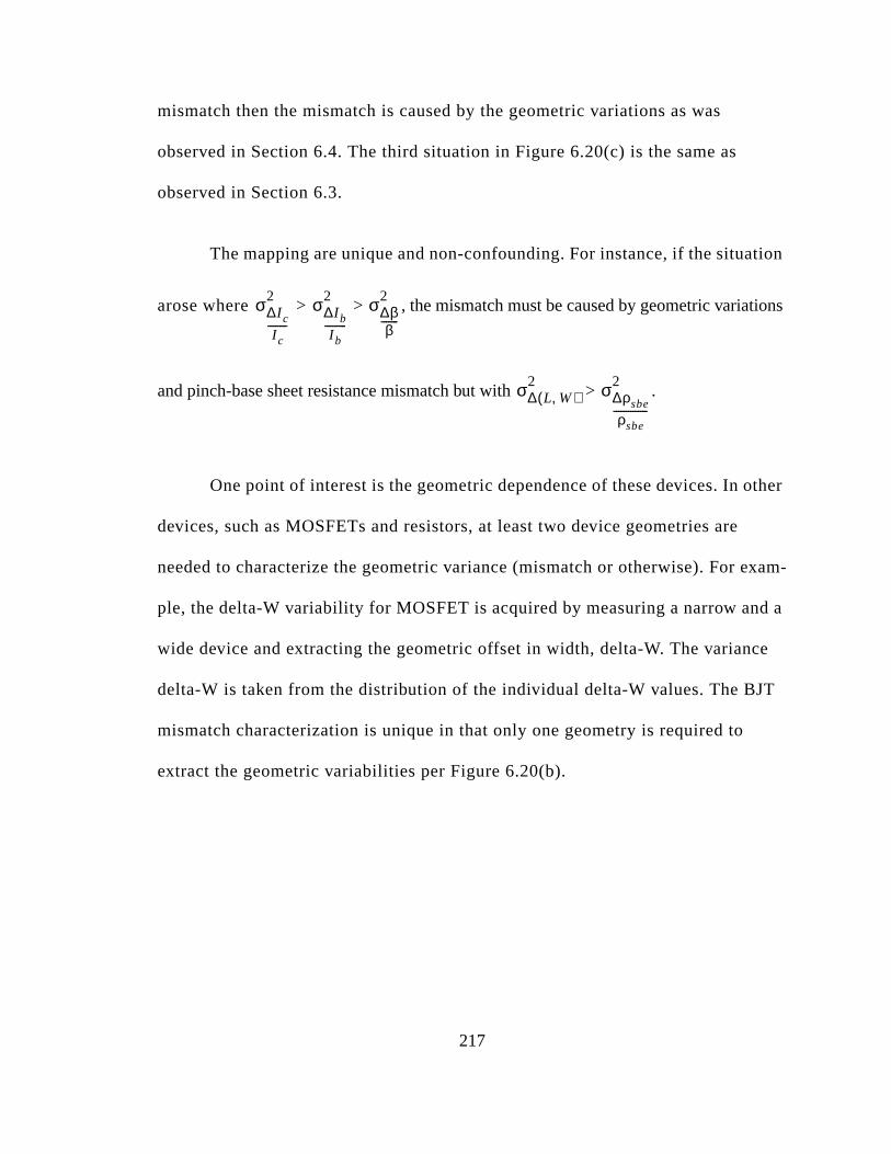
ion
ns
ther
xam-
d a
e
T
mismatch then the mismatch is caused by the geometric variations as was
observed in Section 6.4. The third situation in Figure 6.20(c) is the same as
observed in Section 6.3.
The mapping are unique and non-confounding. For instance, if the situat
arose where > > , themismatch must be caused by geometric variatio
and pinch-base sheet resistance mismatch but with > .
One point of interest is the geometric dependence of these devices. In o
devices, such as MOSFETs and resistors, at least two device geometries are
needed to characterize the geometric variance (mismatch or otherwise). For e
ple, the delta-W variability for MOSFET is acquired by measuring a narrow an
wide device and extracting the geometric offset in width, delta-W. The varianc
delta-W is taken from the distribution of the individual delta-W values. The BJ
mismatch characterization is unique in that only one geometry is required to
extract the geometric variabilities per Figure 6.20(b).
σ∆I c
I c--------
2 σ∆I b
I b---------
2 σ∆ββ
-------
2
σ∆ L W,( )2 σ∆ρsbe
ρsbe--------------
2
217
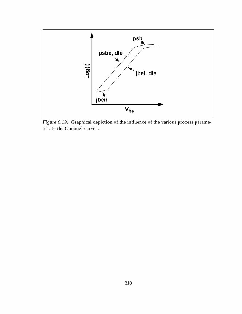
e-
Figure 6.19: Graphical depiction of the influence of the various process paramters to the Gummel curves.jbei, dle
psbe, dle
jben
psb
Log(
I)
Vbe
218
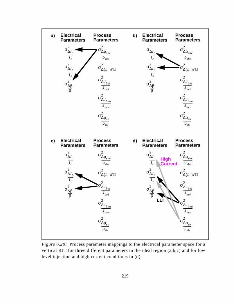
or aow
Figure 6.20: Process parameter mappings to the electrical parameter space fvertical BJT for three different parameters in the ideal region (a,b,c) and for llevel injection and high current conditions in (d).
a)
σ∆I b
I b---------
2
σ∆ββ
-------
2
σ∆I c
I c--------
2
σ∆ L W,( )2
σ∆Jbei
Jbei-------------
2
σ∆ρsbe
ρsbe--------------
2
σ∆Jben
Jben--------------
2
σ∆ρsb
ρsb------------
2
ProcessElectricalParameters Parameters
b)
σ∆I b
I b---------
2
σ∆ββ
-------
2
σ∆I c
I c--------
2
σ∆ L W,( )2
σ∆Jbei
Jbei-------------
2
σ∆ρsbe
ρsbe--------------
2
σ∆Jben
Jben--------------
2
σ∆ρsb
ρsb------------
2
ProcessElectricalParameters Parameters
c)
σ∆I b
I b---------
2
σ∆ββ
-------
2
σ∆I c
I c--------
2
σ∆ L W,( )2
σ∆Jbei
Jbei-------------
2
σ∆ρsbe
ρsbe--------------
2
σ∆Jben
Jben--------------
2
σ∆ρsb
ρsb------------
2
ProcessElectricalParameters Parameters
d)
σ∆I b
I b---------
2
σ∆ββ
-------
2
σ∆I c
I c--------
2
σ∆ L W,( )2
σ∆Jbei
Jbei-------------
2
σ∆ρsbe
ρsbe--------------
2
σ∆Jben
Jben--------------
2
σ∆ρsb
ρsb------------
2
ProcessElectricalParameters Parameters
LLI
HighCurrent
219
mod-
nce
he
ra-
abil-
cing
to
on
e
lan-
junc-
y
mbi-
mis-
ible
t
Chapter 7 Conclusions
This thesis presented several advancements in the status of mismatch
eling and characterization. A mismatch analysis for a bandgap voltage refere
showed that there is an optimum ratio in the resistors and BJTs to minimize t
impact of the mismatch variability on the reference voltage stability over tempe
ture. An analysis of a voltage scaling, resistor ladder DAC showed that the st
ity of the output voltage depends on the bit selection.
An experimental design was presented to cover the geometric and spa
dependencies of mismatch which is applicable for transistors and resistors.
A geometrically based model for resistor mismatch was developed. The
added terms for width-only and length-only effects allow the mismatch model
properly cover the entire geometric space. Modifications were made the comm
mismatch plot of mismatch standard deviation versus 1/sqrt(area) to reflect th
geometric asymmetry. It was discovered that there is a trade-off in the ion imp
tation dose mismatch variability and the junction depth mismatch variability in
terms of the sheet resistance mismatch. Although the dose concentration and
tion depth are independent parameters, the two tend to be inversely related b
technology design convention. Thus, an optimum dose and junction depth co
nation to minimize the sheet resistance mismatch contribution to the resistor
match was found. It was demonstrated through simulated data, that it is poss
to collect mismatch data for dissimilar geometries. This could lead to compac
220
is-
ses,
ct,
esis-
the
cess
and
s-
mismatch test structures and higher order modeling and characterization of m
match.
The new BPV model for MOSFETs successfully modeled the mismatch
behavior over the linear and saturation regions, the mismatch over the gate bia
the anomalous behavior over gate lengths produced by the short channel effe
and the effect over gate length and gate bias produced by the source series r
tance mismatch. The inference of the process parameter mismatches allows
technology developer to pinpoint the contributing process parameters for pro
improvement. This model is a significant advancement over existing models.
The BJT BPV model showed good predictive ability across the biases,
geometries and temperatures. A new technique for the rapid evaluation of the
underlying cause of BJT mismatch was presented. Results over temperature,
collector bias showed that neither parameter had a profound effect on the mi
match.
221

sis-
rgoot,c.6,
J.
edp.
olid
sure-icon-
l
7,
gech
is-
8 References
[1] H. P. Tuinhout, “Transistor matching test structures,” Tutorial Notes from the 1997IEEE ICMTS, March 1997.
[2] M. J. Pelgrom, A. C.Duinmaijer, A. P. Welbers, “Matching properties of MOS trantors,” IEEE J. Solid State Circuits, vol. 24, pp. 1433-1440, Oct. 1989.
[3] J. Bastos, M. Steyaert, R. Roovers, P. Kinget, W. Sansen, B. Graindourze, A. Peand Er. Janssens, “Mismatch characterization of small size MOS transistors,” ProIEEE 1995 Int. Conference on Microelectronic Test Structures, vol. 8, pp. 271-27March 1995.
[4] P. E. Allen, and D. R. Holberg,Voltage Scaling D-A Converter, New York, Holt, Rine-hart, and Wilson, 1987.
[5] P. R. Gray and R. G. Meyer,Analysis and Design of Analog Integrated Circuits, thirdedition, New York, John Wiley & Sons, 1977.
[6] J. B. Shyu, G. C. Temes, and K. Yao, “Random errors in MOS capacitors,” IEEE Solid State Circuits, vol. SC-17, pp. 948-955, Dec. 1982.
[7] J. B. Shyu, G. C. Temes, and F. Krummenacher, “Random error effects in matchMOS capacitors and current sources,” IEEE J. Solid State Circuits, vol. SC-19, p1070-1076, Dec. 1984.
[8] K. R. Lakshmikumar, R. A. Hadaway, and M.A. Copeland, “Characterization andmodeling of mismatch in MOS transistors for precision analog design,” IEEE J. SState Circuits, vol. SC-21, pp. 1057-1066, Dec. 1986.
[9] H. P. Tuinhout, H. Elzinga, J. T. Brugman, and F. Postma, “The floating gate meament technique for characterization of capacitor matching,” IEEE Trans. on Semductor Manufacturing, vol. 9, pp. 2-8, Feb. 1996.
[10] H. Tuinhout, M. Pelgrom, R. Penning de Vries, and M Vertregt, “Effects of metacoverage on MOSFET matching,” Proc. 1996 IEEE IEDM, pp. 735-8, December1996.
[11] H. Tuinhout, “Design of matching test structures,” Proc. 1994 IEEE ICMTS, Vol.pp. 21-27, March 1994.
[12] H. P. Tuinhout and M. Vertregt, “Test structures for investigation of metal coveraeffects on MOSFET matching,” Proc. 1997 IEEE ICMTS, Vol. 10, pp. 179-83, Mar1997.
[13] H. Elzinga, “On the impact of spatial parametric variations on MOS transistor m
hold. 75-
es on
ment
t on,
29,
ing,
3.
S
S
ns4,
match,” Proc 1996 IEEE ICMTS, Vol. 9, pp. 173-7, March 1996.
[14] A. Pavasovic, A. G. Andreou, and C. R. Westgate, "Characterization of subthresmismatch in transistors for VLSI systems," Journal of VLSI Signal Processing, pp85, 1994.
[15] R. C. Jaeger, R. Ramani, and J. C. Suhling, “Effects of stress-induced mismatchCMOS analog circuits,” SRC Pub. C95177, June 1995.
[16] J. Bastos, M. Steyaert, B. Graindourze, and W. Sansen, “Influence of die attachon MOS transistor matching,” Proc. 1996 IEEE ICMTS, Vol. 9, pp. 27-31, March1996.
[17] J. Bastos, M. Steyaert, A. Pergoot, and W. Sansen, “Influence of die attachmenMOS transistor matching,” IEEE Trans. on Semiconductor Manufacturing, Vol. 10pp. 209-218, May 1997.
[18] T. L. Tewksbury and H. S. Lee, “Characterization, modeling and minimization oftransient threshold voltage shifts in MOSFETs,” IEEE J. Solid-State Circuits, Vol.pp. 239-52, March 1994.
[19] C. C. McAndrew, J. Bates, R. T. Ida, and P. Drennan, “Efficient statistical modelwhy β is more than Ic/Ib,” Proc. 1997 IEEE BCTM, pp. 28-31, Oct. 1997.
[20] A. Paupolis,Probability, Random Variables, and Stochastic Processes, New York,McGraw Hill, 1991.
[21] C. Michael, H. Su, M. Ismail, A. Kankunnen, and M. Valtonen, “Statistical designand optimization of analog MOS integrated circuits,” SRC Pub C93629, Dec. 199
[22] C. Michael and M. Ismail, “Statistical modeling of device mismatch for analog MOintegrated circuits,” J. Solid State Circuits, vol. 27, pp.154-166, Feb. 1992.
[23] H.Y. To, C. Michael, and M. Ismail, “Worst case analysis of low-voltage analog MOintegrated circuits,” SRC Pub. 94277, May 1994.
[24] G. E. P. Box, W. G. Hunter, and J. S. Hunter,Statistics for Experimenters. New York,John Wiley and Sons, 1978.
[25] J. K. Kibarian and A. J. Strojwas, “Using spatial information to analyze correlatiobetween test structure data,” IEEE Trans on Semiconductor Manufacturing, Vol. pp.219-225, August 1991.
[26] S. Wolf and R. N. Tauber,Silicon Processing for the VLSI Era: Volume 1 - Process
223

rs
lud-lec.
OS
l
iC-
S
orEE
cir-
n an2,
er-is-
T
8,
Technology, Sunset Beach, CA, Lattice Press, 1987.
[27] H.Y. To and M. Ismail, “Parameter mismatch characterization of bipolar transistofabricated in MOSIS,” SRC Pub. C95025, Feb. 1995.
[28] S. Inohira, T. Shinmi, M. Nagata, T. Toyabe, and K. Iida, “A statistical model incing parameter matching for analog integrated circuit simulation,” IEEE Trans. on EDevices, vol. ED-32, pp. 2177-2183, Oct. 1985.
[29] H. Su, C. Michael, and M. Ismail, “A systematic approach for sizing of analog Mintegrated circuit including transistor mismatch,” SRC Pub. C94530, Nov. 1994.
[30] H. Y. To and M. Ismail, “A novel sensitivity analysis technique for VLSI statisticadesign,” SRC Pub. C95026, Feb. 1995.
[31] F. Larsen and M. Ismail, “A complete analog characterization of Orbit’s n-well BMOS process available through MOSIS,” SRC Pub C94524, Nov. 1994.
[32] H. Y. To and M. Ismail, “A new algorithm for the worst-case analysis of analog MOintegrated circuits,” SRC Pub. C93649, Dec. 1993.
[33] C Abel, C. Michael, M. Ismail, C. S. Teng, R. Lahri, “Characterization of transistmismatch for statistical CAD of submicron CMOS analog circuits,” Proc. 1993 IEInt’l Symp. on Circuits and Systems, Vol.2 , pp. 1401-1404, May 1993.
[34] H. Su, C. Michael, and M. Ismail, “Yield optimization of analog MOS integrated cuits including transistor mismatch,” Proc. 1993 IEEE Int’l Symp. on Circuits andSystems, Vol.2 , pp. 1801-1804, May 1993.
[35] R. W. Gregor, “On the relationship between topography and transistor matching ianalog CMOS technology,” IEEE Trans. on Electron Devices, vol. 39, pp. 275-28Feb. 1992
[36] M. Steyaert, J. Bastos, R. Roovers, P. Kinget, W. Sansen, B. Graindourze, A. Pgoot, and E. Janssens, “Threshold voltage mismatch in short-channel MOS transtors,” Electronics Letters, vol. 30, pp. 1546-1548, Sept. 1994.
[37] S. Wolf,Silicon Processing for the VLSI Era: Volume 3 - The Submicron MOSFE,Sunset Beach, CA, Lattice Press, 1995.
[38] A. Pergoot, B. Graindourze, E. Janssens, J. Bastos, M. Steyaert, P. Kinget, R.Roovers, and W. Sansen, “Statistics for matching,” Proc. 1995 IEEE ICMTS, vol.pp. 193-197, Mar. 1995.
224

of
stors6.
OSal
ron
per-. 9,
g. 39-
is-
ensa-EE
7.
trixrch
et-ndFeb.
[39] J. Bastos, M. Steyaert, A. Pergoot, and W. Sansen, "Mismatch characterizationsubmicron MOS transistors," Analog Integrated Circuits and Signal Processing,vol.12, pp. 95-106, Feb. 1997.
[40] J. Bastos, M. Steyaert, B. Graindourze, and W. Sansen, “Matching of MOS transiwith different layout styles,” Proc 1996 IEEE ICMTS, Vol. 9, pp. 17-18, March 199
[41] F. Forti and M. E. Wright, “Measurement of MOS current mismatch in the weakinversion region,” IEEE J. Solid State Circuits, vol. 29, pp. 138-142, Feb. 1994.
[42] T. Serrano-Gotarredona, B. Linares-Barranco, "Cheap and easy systematic CMtransistor mismatch characterization," Proceedings of the 1998 IEEE InternationSymposium on Circuits and Systems, vol. 2, pp.466-469, June 1998.
[43] T. Serrano-Gotarredona, B. Linares-Barranco, "A `do-it-yourself' methodology foCMOS transistor mismatch characterization," Proceedings of Midwest SymposiumCircuits and Systems, vol. 2, pp.1120-1123, Aug. 1997.
[44] S. C. Wong, K. H. Pan, D. J. Ma, M. S. Liang, and P. N. Tseng, “On matching proties and process factors for submicrometer CMOS,” Proc 1996 IEEE ICMTS, volpp. 43-47, March 1996.
[45] S. C. Wong, K. H. Pan, and D. J. Ma, "A CMOS mismatch model and scalingeffects," IEEE EDL, vol. 18, pp. 261-263, June 1997.
[46] S. J. Lovett, R. Clancy, M. Welton, A. Mathewson, and B. Mason, “Characterizinthe mismatch of submicron MOS transistors,” Proc 1996 IEEE ICMTS, vol. 9, pp42, March 1996.
[47] S. J. Lovett, M. Welten, A. Mathewson, B. Mason, "Optimizing MOS transistor mmatch," IEEE Journal of Solid-State Circuits vol.33, pp.147-50, Jan. 1998.
[48] E. S. Karhunen, F. V. Fernandez, A. R. Vazquez, "Mismatch distance term comption in centroid configurations with nonzero-area devices," Proceedings of 1997 IEInternational Symposium on Circuits and Systems, vol.3, p.1644-1647, June 199
[49] L. Portmann, C. Lallement, F. Krummenacher, "A high density integrated test maof MOS transistors for matching study," Proc. of 1998 IEEE ICMTS, p.19-24, Ma1998.
[50] T. Ohzone, T. Miyakawa, T. Matsuda, T. Yabu, S. Odanaka, "Influence of asymmric/symmetric source/drain region on asymmetry and mismatch of CMOSFET's acircuit performance," IEEE Transactions on Electron Devices vol.45, pp.529-537,1998.
225

tion-
S
nd7
on
OS96
risa-99.
is-5.
the
on8.
.
on8.
EE
ys-
[51] T. Ohzone, T. Miyakawa, T. Matsuda, T. Yabu, S. Odanaka, "Performance evaluaof CMOS ring-oscillators with source/drain regions fabricated by asymmetric/symmetric ion-implantation," 1997 IEEE International Conference on MicroelectronicTest Structures Proceedings, pp.131-136, March 1997.
[52] M. J. M. Pelgrom, H. P. Tuinhout, M. Vertregt, "Transistor matching in analog CMOapplications," Proc. 1998 IEEE IEDM, pp.915-18, Dec 1998.
[53] H. P. Tuinhout, A. H. Montree, J. Schmitz, P. A. Stolk, "Effects of gate depletion aboron penetration on matching of deep submicron CMOS transistors," Proc. 199IEEE IEDM, pp.631-634, Dec. 1997.
[54] H. Elzinga, "Using test structures to assess the impact of critical process steps MOS transistor matching," Proc. 1998 IEEE ICMTS, pp.119-122, March 1998.
[55] M. Bolt, E. Cantatore, M. Socha, C. Aussems, J. Solo, “Matching properties of Mtransistors and delay line chains with self-aligned source/drain contacts,” Proc 19IEEE ICMTS, Vol. 9, pp. 21-25, March 1996.
[56] H. P. Tuinhout, “Transistor matching: test structures and techniques for charactetion of transistor matching,” Tutorial Notes from the 1999 IEEE ICMTS, March 19
[57] S. C. Wong, J. K. Ting, and S. L. Hsu, “Characterization and modeling of MOS mmatch in analog CMOS technology,” Proc. 1995 IEEE ICMTS, Vol. 8, March 199
[58] M. Niewczas, “Characterization of the threshold voltage variation: a test chip andresults,” Proc. 1997 IEEE ICMTS, vol. 10, pp. 169-172, March 1997.
[59] H. P. Tuinhout, W. C. M. Peters, "Measurement of lithographical proximity effectsmatching of bipolar transistors," Proc. of 1998 IEEE ICMTS, pp.7-12, March 199
[60] H. P. Tuinhout, M. Vertregt, "Test structures for investigation of metal coverageeffects on MOSFET matching," Proc. 1997 IEEE ICMTS, p.179-183, March 1997
[61] H. P. Tuinhout, W. C. M. Peters, "Measurement of lithographical proximity effectsmatching of bipolar transistors," Proc. of 1998 IEEE ICMTS, pp.7-12, March 199
[62] S. Wong, K. Pan, and D. Ma, "A CMOS mismatch model and scaling effects," IEElectron Device Letters vol.18, pp.261-263, June 1997.
[63] Y. Cheng, M. C. Jeng, Z. Liu, J. Huang, M. Chan, K. Chen, P. K. Ko, C. Hu, "A phical and scalable I-V model in BSIM3v3 for analog/digital circuit simulation," IEEETrans. on Electron Devices vol. 44, pp.277-87, Feb 1997.
226

e-
pp.
orch
is-
, pp.
[64] D. W. Marquardt, "An algorithm for least-squares estimation of nonlinear paramters" SIAM J. Appl. Math., vol. 11, pp.431-441, 1963.
[65] H. P. Tuinhout, “Transistor Matching: Characterization of differences betweenclosely spaced identical transistors,” Tutorial Notes from the 1998 IEEE ICMTS, 6-1 - 6-38, March 1998.
[66] S. D. Connor and D. Evanson, “Automated Extraction of Matching Parameters fBipolar Transistor Technologies,” Proc. 1996 IEEE ICMTS, vol. 9, pp. 33-38, Mar1996.
[67] P. G. Drennan, C. C. McAndrew, and J. Bates, “A comprehensive vertical BJT mmatch model,” Proc. 1998 IEEE BCTM, pp. 83-86, Oct. 1998.
[68] W. F. Davis and R. T. Ida, “Statistical IC simulation based on independent waferextracted process parameters and experimental designs,” Proc. 1989 IEEE BCTM262-265, Oct 1989.
227