Int. J. Engg. Res. & Sci. & Tech. 2014 M Meena and B ... · Int. J. Engg. Res. & Sci. & Tech. 2014...
13
Transcript of Int. J. Engg. Res. & Sci. & Tech. 2014 M Meena and B ... · Int. J. Engg. Res. & Sci. & Tech. 2014...

327
This article can be downloaded from http://www.ijerst.com/currentissue.php
Int. J. Engg. Res. & Sci. & Tech. 2014 M Meena and B Kishore Kumar, 2014
HIGH SPEED AND REDUCED AREA REALIZATIONOF EDDR ARCHITECTURE
M Meena1* and B Kishore Kumar2
While focusing on the testing of MECA in a video coding system, this work presents an Built inSelf Detection and Correction (BISDC) design, based on the Residue-and-Quotient (RQ) code,to embed into ME for video coding testing applications. An error in Processing Elements (PEs),i.e. key components of a ME, can be detected and recovered effectively by using the proposedBISDC design. Experimental results indicate that the proposed BISDC design for ME testingcan detect errors and recover data. The functional verification and synthesis can be done byXilinx ISE 12.3 Version.
Keywords: Processing Element (PE), Built in Self-Detection and Correction (BISDC), MotionEstimation (ME), Residue-and-Quotient Code Generation (RQCG), Test CodeGenerator (TCG)
*Corresponding Author: M Meena [email protected]
INTRODUCTIONThe new Joint Video Team (JVT) video coding
standard has garnered increased attention
recently. Generally, Motion Estimation Computing
Array (MECA) performs up to 50% of
computations in the entire video coding system,
and is typically considered the computationally
most important part of video coding systems.
Thus, integrating the MECA into a System-On-
Chip (SOC) design has become increasingly
important for video coding applications.
Additionally, the visual quality and Peak Signal-
to-Noise Ratio (PSNR) at a given bit rate are
influenced if an error occurred in ME process.
1 M.Tech Student, JB Institute of Engineering & Technology, Bhaskar Nagar, Moinabad Mandal 500075, RR District, Hyderabad, India.2 Assistant Professor, JB Institute of Engineering & Technology, Bhaskar Nagar, Moinabad Mandal 500075, RR District, Hyderabad, India.
Int. J. Engg. Res. & Sci. & Tech. 2014
ISSN 2319-5991 www.ijerst.comVol. 3, No. 4, November 2014
© 2014 IJERST. All Rights Reserved
Research Paper
Although advances in VLSI technology allow
integration of a large number of Processing
Elements (PEs) in an MECA into an SOC, this
increases the logic-per-pin ratio, thereby
significantly decreasing the efficiency of chip logic
testing. For a commercial chip, a video coding
system must introduce Design For Testability
(DFT), especially in an MECA.
The objective of DFT is to increase the ease
with which a device can be tested to guarantee
high system reliability. Many DFT approaches
have been developed. These approaches can be
divided into three categories: ad hoc (problem
oriented), structured, and Built-In Self-Test (BIST).

328
This article can be downloaded from http://www.ijerst.com/currentissue.php
Int. J. Engg. Res. & Sci. & Tech. 2014 M Meena and B Kishore Kumar, 2014
Among these techniques, BIST has an obvious
advantage in that expensive test equipment is not
needed and tests are low cost.
BIST schemes not only detect faults but also
specify their location for error correcting. BIST
can generate test simulation and test responses
without outside support. The extended BIST
schemes generally focus on memory circuit,
testing-related issues of video coding have been
addressed. Thus, exploring the feasibility of an
embedded testing approach to detect errors and
recover data of a ME is of worthwhile interest.
Additionally, the reliability issue of numerous
PEs in a ME can be improved by enhancing the
capabilities of Concurrent Error Detection (CED).
The CED approach can detect errors through
conflicting and undesired results generated from
operations on the same operands. CED can also
test the circuit at full operating speed without
interrupting a system. Thus, based on the CED
concept, this work develops an BISDC
architecture based on the RQ code to detect
errors and recovery data in PEs of a ME.
MOTION ESTIMATIONExisting System
The Motion Estimation Computing Array is used
in Video Encoding applications to calculate the
best motion between the current frame and
reference frames. The MECA is in decoding
application occupies large amount of area (LUT)
and timing penalty. By introducing the concept of
Built-in Self test technique the area overhead is
increased in less amount of area.
Proposed system
In this Project the Built-in Self test Technique
(BIST) is included in the MECA and in each of
Processing Element in MECA. Thus by
introducing the BIST Concept the testing is done
internally without Connecting outside testing
Requirements. So the area (LUT) required is also
reduces. And in this Project the Errors in MECA
are calculated and the concept of diagnoses, i.e.,
self detect and self repair concepts are
introduced.
Block Matching Motion Estimation
Several different algorithms derived from various
theories, including object-oriented tracking, exist
to perform motion estimation. Among them, one
of the most popular algorithms is the Block
Matching Motion Estimation (BME) algorithm.
BME treats a frame as being composed of many
individual sub-frame blocks, known as macro
Blocks. Motion vectors are then used to encode
the motion of the macro Blocks through frames
of video via a frame by frame matching process.
When a frame is brought into the encoder for
compression, it is referred to as the current
frame. It is the goal of the BME unit to describe
the motion of the macro Blocks within the current
frame relative to a set of reference frames. The
reference frames may be previous or future
frames relative to the current frame. Each
reference frame is also divided into a set of sub
frame blocks, which are equal to the size of the
macro Blocks. These blocks are referred to as
reference Blocks.
The BME algorithm wil l scan several
candidate reference Blocks within a reference
frame to find the best match to a macro Block.
Once the best reference Block is found a motion
vector is then calculated to record the
spatial displacement of the macro Block relative
to the matching reference Block, as shown in
Figure 1.

329
This article can be downloaded from http://www.ijerst.com/currentissue.php
Int. J. Engg. Res. & Sci. & Tech. 2014 M Meena and B Kishore Kumar, 2014
Search Windows
When searching a reference frame for possible
macro Block matches, the entire reference frame
is not searched. Instead the search is restricted
within a search window. Search windows in most
H.264 implementations have a size of 48-pixel
(rows) x 63-pixel (columns). In this Paper, we use
the same 48 x 63 search window size. This
window consists of a vertical search range of [-
16, +16] and a horizontal search range of [-24,
+23] pixels as illustrated in Figure 2.
In the Figure 2, the dashed large rectangle in
the reference frame represents the 48 x 63 search
window area. The dashed square in the top left
corner of the search window represents the first
of the 1,584 possible candidate 16 x 16 reference
Blocks. Each subsequent reference Block is
offset by either one pixel row or one pixel column
from its predecessor while the entire search
window area is covered by the overlapping
candidate reference Blocks. Note that the original
16 x 16 macro Block is positioned at the centre
of the search window. In order to compare it to
every candidate reference Block within the search
window, the macro Block has a maximum
displacement of 24 pixels to the left, 23 pixels to
Figure 1: Block Matching between Current and Reference Frames
Figure 2: Search Window Size Definition

330
This article can be downloaded from http://www.ijerst.com/currentissue.php
Int. J. Engg. Res. & Sci. & Tech. 2014 M Meena and B Kishore Kumar, 2014
the right, 16 pixels up, and 16 pixels down from
its original position – resulting in a horizontal
search range of [-24, +23] and a vertical search
range of [-16, +16].
RQ Code Generation
Coding approaches such as parity code, Berger
code, and residue code have been considered
for design applications to detect circuit errors.
Residue code is generally separable arithmetic
codes by estimating a residue for data and
appending it to data. Error detection logic for
operations is typically derived by a separate
residue code, making the detection logic is simple
and easily implemented. Error detection logic for
operations is typically derived using a separate
residue code such that detection logic is simply
and easily implemented. However, only a bit error
can be detected based on the residue code.
Additionally, an error can’t be recovered effectively
by using the residue codes. Therefore, this work
presents a quotient code, which is derived from
the residue code, to assist the residue code in
detecting multiple errors and recovering errors.
The corresponding circuit design of the RQCG
is easily realized by using the simple adders
(ADDs). Namely, the RQ code can be generated
with a low complexity and little hardware cost.
The mathematical model of RQ code is simply
described as follows. Assume that binary data X
is expressed as
1
1 2 2 1 00
{ ... } 2n
jn n j
j
X b b b b b b
...(1)
The RQ code of X modulo m expressed as R
= |X|m, Q = [X/m], respectively. Notably [i] denotes
the largest integer not exceeding i.
According to the above RQ code expression,
the corresponding circuit design of the RQCG
can be realized. In order to simplify the complexity
of circuit design, the implementation of the
module is generally dependent on the addition
operation. Additionally, based on the concept of
residue code, the following definitions shown can
be applied to generate the RQ code for circuit
design.
Definition 1:
|N1 + N2|m = ||N1|m + |N2|m|m ...(2)
Definition 2:
Let Nj = n1 + n2+…+nj, then
|Nj|m = ||n1|m + |n2|m…+|nj|m|m ...(3)
To accelerate the circuit design of RQCG, the
binary data shown in (1) can generally be divided
into two parts:
1
0
2n
jj
j
X b
1 1
0
2 2 2n n
j j k kj j
j j k
b b
0 12kY Y ...(4)
Significantly, the value of k is equal to [n/2]
and the data formation of Y0 and Y1 are a decimal
system. If the modulus m = 2k – 1, then the
residue code of modulo is given by
R = |X|m
= |Y0 + Y1|m = |Z0 + Z1|m = (Z0 + Z1) ...(5)
XQ
m
0 1 0 11 1 1
Y Y Z ZQ Y Z Y
m m
1 1Z Y ...(6)
331
This article can be downloaded from http://www.ijerst.com/currentissue.php
Int. J. Engg. Res. & Sci. & Tech. 2014 M Meena and B Kishore Kumar, 2014
0 1
0 1
0(1),( )
1(0),
if Z Z m
if Z Z m
Notably, since the value of Y0 + Y1 is generally
greater than that of modulus m, the equations in
(5) and (6) must be simplified further to replace
the complex module operation with a simple
addition operation by using the parameters Z0,
Z1, and .
Based on (5) and (6), the corresponding circuit
design of the RQCG is easily realized by using
the simple adders (ADDs). Namely, the RQ code
can be generated with a low complexity and little
hardware cost.
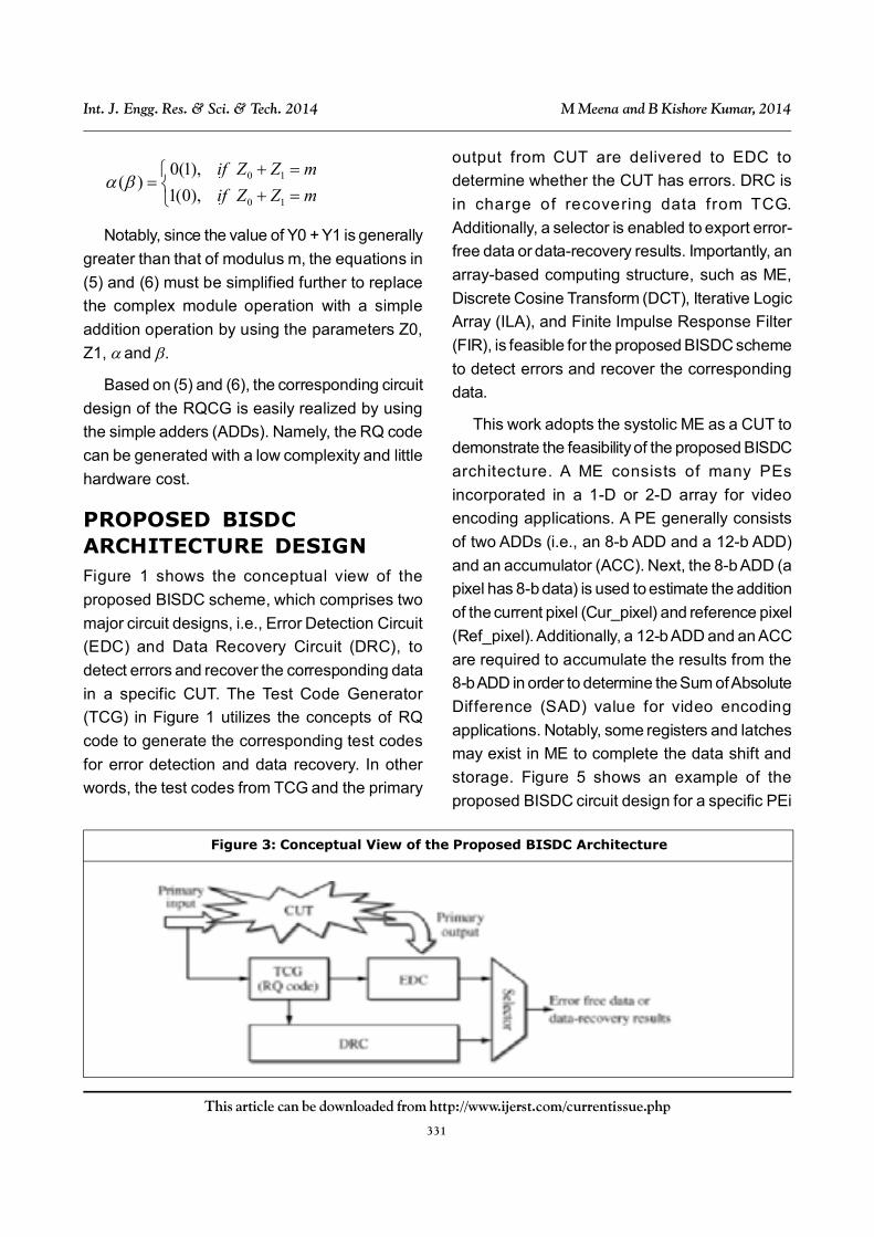
PROPOSED BISDCARCHITECTURE DESIGNFigure 1 shows the conceptual view of the
proposed BISDC scheme, which comprises two
major circuit designs, i.e., Error Detection Circuit
(EDC) and Data Recovery Circuit (DRC), to
detect errors and recover the corresponding data
in a specific CUT. The Test Code Generator
(TCG) in Figure 1 utilizes the concepts of RQ
code to generate the corresponding test codes
for error detection and data recovery. In other
words, the test codes from TCG and the primary
output from CUT are delivered to EDC to
determine whether the CUT has errors. DRC is
in charge of recovering data from TCG.
Additionally, a selector is enabled to export error-
free data or data-recovery results. Importantly, an
array-based computing structure, such as ME,
Discrete Cosine Transform (DCT), Iterative Logic
Array (ILA), and Finite Impulse Response Filter
(FIR), is feasible for the proposed BISDC scheme
to detect errors and recover the corresponding
data.
This work adopts the systolic ME as a CUT to
demonstrate the feasibility of the proposed BISDC
architecture. A ME consists of many PEs
incorporated in a 1-D or 2-D array for video
encoding applications. A PE generally consists
of two ADDs (i.e., an 8-b ADD and a 12-b ADD)
and an accumulator (ACC). Next, the 8-b ADD (a
pixel has 8-b data) is used to estimate the addition
of the current pixel (Cur_pixel) and reference pixel
(Ref_pixel). Additionally, a 12-b ADD and an ACC
are required to accumulate the results from the
8-b ADD in order to determine the Sum of Absolute
Difference (SAD) value for video encoding
applications. Notably, some registers and latches
may exist in ME to complete the data shift and
storage. Figure 5 shows an example of the
proposed BISDC circuit design for a specific PEi
Figure 3: Conceptual View of the Proposed BISDC Architecture

332
This article can be downloaded from http://www.ijerst.com/currentissue.php
Int. J. Engg. Res. & Sci. & Tech. 2014 M Meena and B Kishore Kumar, 2014
of a ME. The fault model definition, RQCG-based
TCG design, operations of error detection and
data recovery, and the overall test strategy are
described carefully as follows:
SAD Tree
PEs utilizing the concept of the proposed SAD
Tree architecture. The proposed SAD Tree is a
2-D intra-level architecture and consists of a 2-D
PE array and one 2-D adder tree with propagation
registers Current pixels are stored in each PE,
and reference pixels are stored in propagation
registers for data reuse. In each cycle, current
and reference pixels are inputted to PEs.
Simultaneously, continuous reference pixels in a
row are inputted into propagation registers to
update reference pixels. In propagation registers,
reference pixels are propagated in the vertical
direction row by row. In SAD Tree architecture,
all distortions of a searching candidate are
generated in the same cycle, and by an adder
tree, distortions are accumulated to derive the
SAD in one cycle.
Fault Model
The PEs are essential building blocks and are
connected regularly to construct a ME. Generally,
PEs are surrounded by sets of ADDs and
accumulators that determine how data flows
through them. PEs can thus be considered the
class of circuits called ILAs, whose testing
assignment can be easily achieved by using the
fault model, Cell Fault Model (CFM). Using CFM
has received considerable interest due to
accelerated growth in the use of high-level
synthesis, as well as the parallel increase in
complexity and density of Integration Circuits
(ICs). Using CFM makes the tests independent
of the adopted synthesis tool and vendor library.
Arithmetic modules, like ADDs (the primary
element in a PE), due to their regularity, are
designed in an extremely dense configuration.
Moreover, a more comprehensive fault model,
i.e., the Stuck-At (SA) model, must be adopted to
cover actual failures in the interconnect data bus
between PEs. The SA fault is a well known
structural fault model, which assumes that faults
cause a line in the circuit to behave as if it were
permanently at logic “0” (stuck-at 0 (SA0)) or logic
“1” [stuck-at 1 (SA1)]. The SA fault in a ME
architecture can incur errors in computing SAD
values. A distorted computational error (e) and
the magnitude of (e) are assumed here to be equal
to SAD|- SAD, where SAD| denotes the computed
SAD value with SA faults.
Figure 4: SAD Tree Architecture

333
This article can be downloaded from http://www.ijerst.com/currentissue.php
Int. J. Engg. Res. & Sci. & Tech. 2014 M Meena and B Kishore Kumar, 2014
TCG Design
According to Figure 2, TCG is an important
component of the proposed BISDC architecture.
Notably, TCG design is based on the ability of the
RQCG circuit to generate corresponding test
codes in order to detect errors and recover data.
The specific in Figure 2 estimates the absolute
difference between the Cur_pixel of the search
area and the Ref_pixel of the current macro block
Thus, by utilizing PEs, SAD shown in as follows,
in a macro block with size of N X N can be
evaluated:
||1
0
1
0ijij
N
j
N
i
YXSAD
yijyijxijxij
N
j
N
i
rmqrmq
..1
0
1
0
where rxij, qxij and ryij, qyij denote the corresponding
RQ code of Xij and Yij modulo m. Importantly, Xij
and Yij represent the luminance pixel value of
Cur_pixel and Ref_pixel, respectively. Based on
the residue code, the definitions shown in (2) and
(3) can be applied to facilitate generation of the
RQ code (RT and QT) form TCG. Namely, the
circuit design of TCG can be easily achieved (see
Figure 3) by using (8) and (9) we use to derive
the corresponding RQ code.
ijij
N
j
N
iT YXR
1
0
1
0
...01010000 mm
YXYX
mmNNNN YX )1)(1()1)(1(
myyxx rmqrmq 00000000 ..
)1)(1()1)(1( .... NNxNNx rmq
mmNNyNNy rmq )1)(1()1)(1( .
myxmyx rrrr 01010000
Figure 5: A Specific PEi Testing Processes of the Proposed BISDC Architecture

334
This article can be downloaded from http://www.ijerst.com/currentissue.php
Int. J. Engg. Res. & Sci. & Tech. 2014 M Meena and B Kishore Kumar, 2014
mmNNyNNx rr )1)(1()1)(1(
mmNNmmrrr 110100 ... ...(8)
m
YX
Q
N
i
N
jijij
T
1
0
1
0
m
YXYXYX NNNN )1)(1()1)(1(01010000 ...
m
rr
m
mqmq yxyx 00000000 ..
...
.. 01010101
m
rr
m
mqmq yxyx
...01010000 yxyx qqqq
m
rrrr yxyx 01010000...(9)
Figure 6: Circuit Design of the TCG
BISDC Processes
Figure 2 clearly indicates that the operations of
error detection in a specific PEi is achieved by
using EDC, which is utilized to compare the
outputs between TCG and RQCG1 in order to
determine whether errors have occurred. If the
values of RPEi RT and/or QPEi QT, then the
errors in a specific PEi can be detected. The EDC
output is then used to generate a 0/1 signal to
indicate that the tested PEi is error-free/errancy.
This work presents a mathematical statement
to verify the operations of error detection. Based
on the definition of the fault model, the SAD value
is influenced if either SA1 and/or SA0 errors have
occurred in a specific PEi. In other words, the
SAD value is transformed to SAD’ = SAD +e if an
error occurred. Notably, the error signal e is
expressed as
e = qe.m+re ...(10)
to comply with the definition of RQ code. Under
335
This article can be downloaded from http://www.ijerst.com/currentissue.php
Int. J. Engg. Res. & Sci. & Tech. 2014 M Meena and B Kishore Kumar, 2014
the faulty case, the RQ code from RQCG2 of the
TCG is still equal to (8) and (9). However, RPEi
and QPEi are changed to (13) and (14) because
an error e has occurred. Thus, the error in a
specific PEi can be detected if and only if (8) (11) and/or (9) (12):
mPE DSARi
m
N
jijij
N
i
eYX
1
0
1
0
mNNmm rrr )1)(1(0100 ...
mmer ...(11)
mPE DSAQi
m
eYXN
jijij
N
i
1
0
1
0
eNN qrqq )1)(1(0100 ...
m
rrrr eNNm )1)(1(0100 ...
During data recovery, the circuit DRC plays a
significant role in recovering RQ code from TCG.
The data can be recovered by implementing the
mathematical model as
TT RQmSAD
TTj RQ )12(
TTT
j RQQ 2 ...(13)
To realize the operation of data recovery in
(13), a Barrel shift and a corrector circuits are
necessary to achieve the functions of (2j X QT)
and (-QT +RT), respectively. Notably, the proposed
BISDC design executes the error detection and
data recovery operations simultaneously.
Additionally, error-free data from the tested PEi
or the data recovery that results from DRC is
selected by a multiplexer (MUX) to pass to the
next specific PEi+1 for subsequent testing.
OVERALL TEST STRATEGYBy extending the testing processes of a specific
PEi in Figure 2 and 4 illustrates the overall BISDC
architecture design of a ME. First, the input data
of Cur_pixel and Ref_pixel are sent
simultaneously to PEs and TCGs in order to
estimate the SAD values and Design of An Error
generate the test RQ code RT and QT. Second,
the SAD value from the tested object PEi, which
is selected by MUX1, is then sent to the RQCG
circuit in order to generate RPEi and QPEi codes.
Meanwhile, the corresponding test codes RTi and
QTi from a specif ic TCGi are selected
simultaneously by MUXs 2 and 3, respectively.
Third, the RQ code from TCGi and RQCG circuits
are compared in EDC to determine whether the
tested object PEi have errors. The tested object
PEi is error-free if and only if RPEi = RTi and QPEi =
QTi. Additionally, DRC is used to recover data
encoded by TCGi, i.e., the appropriate RTi and
QTi codes from TCGi are selected by MUXs 2
and 3, respectively, to recover data. Fourth, the
error-free data or data recovery results are
selected by MUX4. Notably, control signal S4 is
generated from EDC, indicating that the
comparison result is error-free (S4 = 0) or errancy
(S4 = 1). Finally, the error-free data or the data-
recovery result from the tested object PEi is
passed to a De-MUX, which is used to test the
next specific PEi+1; otherwise, the final result is
exported.
336
This article can be downloaded from http://www.ijerst.com/currentissue.php
Int. J. Engg. Res. & Sci. & Tech. 2014 M Meena and B Kishore Kumar, 2014
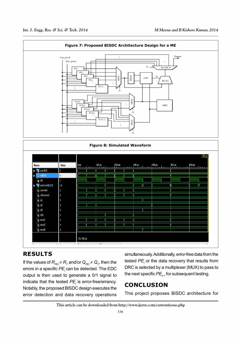
Figure 7: Proposed BISDC Architecture Design for a ME
Figure 8: Simulated Waveform
RESULTSIf the values of RPEi RT and/or QPEi QT, then the
errors in a specific PEi can be detected. The EDC
output is then used to generate a 0/1 signal to
indicate that the tested PEi is error-free/errancy.
Notably, the proposed BISDC design executes the
error detection and data recovery operations
simultaneously. Additionally, error-free data from the
tested PEi or the data recovery that results from
DRC is selected by a multiplexer (MUX) to pass to
the next specific PEi+1 for subsequent testing.
CONCLUSIONThis project proposes BISDC architecture for

337
This article can be downloaded from http://www.ijerst.com/currentissue.php
Int. J. Engg. Res. & Sci. & Tech. 2014 M Meena and B Kishore Kumar, 2014
self-detection and self-correction of errors of PEs
in an ME. Based on the RQ code, a RQCG-based
TCG design is developed to generate the
corresponding test codes to detect errors and
recover data. Performance evaluation reveals that
the proposed BISDC architecture effectively
achieves self-detection and self-correction
capabilities with minimal area (LUT). The
Functional-simulation has been successfully
carried out with the results matching with
expected ones. The design functional verification
and Synthesis is done by using Xilinx-ISE 12.3
Version.
REFERENCES1. Advanced Video Coding for Generic
Audiovisual Services, ISO/IEC 14496-10:2005
(E), Mar. 2005, ITU-T Rec. H.264 (E).
2. Chen C Y, Chien S Y, Huang Y W, Chen T
C, Wang T C, and Chen L G (2006),
“Analysis and architecture design of variable
block-size motion estimation for H.264/
AVC,” IEEE Trans. Circuits Syst. I, Reg.
Papers, Vol. 53, No. 3, pp. 578–593.
3. Dong M Y, Yang S H, and Lu S K (2008),
“Design-for-testability techniques for motion
estimation computing arrays,” in Proc. Int.
Conf. Commun., Circuits Syst., May, pp.
1188–1191.
4. Huang Y W, Hsieh B Y, Chien S Y, Ma S Y,
and Chen L G (2006), “Analysis and
complexity reduction of multiple reference
frames motion estimation in H.264/AVC,”
IEEE Trans. Circuits Syst. Video Technol.,
Vol. 16, No. 4, pp. 507–522.
5. Huang Y S, Yang C J, and Hsu C L (2009),
“C-testable motion estimation design for
video coding systems,” J. Electron. Sci.
Technol., Vol. 7, No. 4, pp. 370–374.
6. Information Technology-Coding of Audio-
Visual Objects—Part 2: Visual, ISO/IEC 14
496-2, 1999.
7. Li D, Hu M, and Mohamed O A (2004), “Built-
in self-test design of motion estimation
computing array,” in Proc. IEEE Northeast
Workshop Circuits Syst., June, pp. 349-352.
8. Wu T H, Tsai Y L, and Chang S J (2007),
“An efficient design-for-testability scheme for
motion estimation in H.264/AVC,” in Proc.
Int. Symp VLSI Design, Autom. Test, Apr.
pp. 1-4.