Insulating phases of vanadium dioxide are Mott-Hubbard ...
19
W&M ScholarWorks W&M ScholarWorks Arts & Sciences Articles Arts and Sciences 2-15-2018 Insulating phases of vanadium dioxide are Mott-Hubbard Insulating phases of vanadium dioxide are Mott-Hubbard insulators insulators T. J. Huffman College of William and Mary, [email protected] C. Hendriks College of William and Mary E. J. Walter College of William and Mary Joonseok Yoon Honglyoul Ju See next page for additional authors Follow this and additional works at: https://scholarworks.wm.edu/aspubs Recommended Citation Recommended Citation Huffman, T. J.; Hendriks, C.; Walter, E. J.; Yoon, Joonseok; Ju, Honglyoul; Smith, R.; Carr, G. L.; Krakauer, H. X.; and Qazilbash, M. M., Insulating phases of vanadium dioxide are Mott-Hubbard insulators (2018). PHYSICAL REVIEW B, 95(7). 10.1103/PhysRevB.95.075125 This Article is brought to you for free and open access by the Arts and Sciences at W&M ScholarWorks. It has been accepted for inclusion in Arts & Sciences Articles by an authorized administrator of W&M ScholarWorks. For more information, please contact [email protected].
Transcript of Insulating phases of vanadium dioxide are Mott-Hubbard ...

W&M ScholarWorks W&M ScholarWorks
Arts & Sciences Articles Arts and Sciences
2-15-2018
Insulating phases of vanadium dioxide are Mott-Hubbard Insulating phases of vanadium dioxide are Mott-Hubbard
insulators insulators
T. J. Huffman College of William and Mary, [email protected]
C. Hendriks College of William and Mary
E. J. Walter College of William and Mary
Joonseok Yoon
Honglyoul Ju
See next page for additional authors
Follow this and additional works at: https://scholarworks.wm.edu/aspubs
Recommended Citation Recommended Citation Huffman, T. J.; Hendriks, C.; Walter, E. J.; Yoon, Joonseok; Ju, Honglyoul; Smith, R.; Carr, G. L.; Krakauer, H. X.; and Qazilbash, M. M., Insulating phases of vanadium dioxide are Mott-Hubbard insulators (2018). PHYSICAL REVIEW B, 95(7). 10.1103/PhysRevB.95.075125
This Article is brought to you for free and open access by the Arts and Sciences at W&M ScholarWorks. It has been accepted for inclusion in Arts & Sciences Articles by an authorized administrator of W&M ScholarWorks. For more information, please contact [email protected].

Authors Authors T. J. Huffman, C. Hendriks, E. J. Walter, Joonseok Yoon, Honglyoul Ju, R. Smith, G. L. Carr, H. X. Krakauer, and M. M. Qazilbash
This article is available at W&M ScholarWorks: https://scholarworks.wm.edu/aspubs/243

This is the accepted manuscript made available via CHORUS. The article has beenpublished as:
Insulating phases of vanadium dioxide are Mott-Hubbardinsulators
T. J. Huffman, C. Hendriks, E. J. Walter, Joonseok Yoon, Honglyoul Ju, R. Smith, G. L. Carr,H. Krakauer, and M. M. Qazilbash
Phys. Rev. B 95, 075125 — Published 15 February 2017DOI: 10.1103/PhysRevB.95.075125

The insulating phases of vanadium dioxide are Mott-Hubbard insulators
T. J. Huffman1, C. Hendriks1, E. J. Walter1, Joonseok Yoon2, Honglyoul Ju2, R. Smith3,
G. L. Carr3, H. Krakauer1, M. M. Qazilbash1,*
1. Department of Physics, College of William and Mary, Williamsburg, VA 23187-8795, USA
2. Department of Physics, Yonsei University, Seoul 120-749, Republic of Korea
3. Photon Sciences, Brookhaven National Laboratory, Upton, NY 11973, USA
We present the first comprehensive broadband optical spectroscopy data on two insulating phases of vanadium dioxide (VO2): monoclinic M2 and triclinic. The main result of our work is that the energy gap and the electronic structure are essentially unaltered by the first-order structural phase transition between the M2 and triclinic phases. Moreover, the optical interband features in the M2 and triclinic phases are remarkably similar to those observed in the well-studied monoclinic M1 insulating phase of VO2. As the energy gap is insensitive to the different lattice structures of the three insulating phases, we rule out vanadium-vanadium pairing (the Peierls component) as the dominant contributor to the opening of the gap. Rather, the energy gap arises primarily from intra-atomic Coulomb correlations.
I. INTRODUCTION
There have been many experimental and theoretical studies of the thermally driven metal-
insulator transition (MIT) between the insulating monoclinic (M1) and the metallic rutile (R)
phases of vanadium dioxide (VO2). Some fraction of these studies attribute the insulating M1
state to the vanadium-vanadium Peierls type pairing (see Fig. 1) that leads to unit cell doubling.
Others argue that the insulating behavior in the M1 phase is primarily a result of Mott-Hubbard
correlations. These studies, reviewed in Refs. [1–3], are too numerous to be referenced here. A
significant proportion of the literature on the nature of insulating VO2, particularly in recent
years [4–17], has struggled to decouple the contributions of the Mott-Hubbard and Peierls
mechanisms because of an emphasis on the M1 phase. Interestingly, it has long been recognized
that measuring the electronic properties of two additional insulating VO2 phases, the monoclinic
2
M2 and triclinic T, could potentially settle the debate about the origin of the energy gap, but the
measurements have been difficult to achieve.
One of our purposes in this paper is to refocus attention to the importance of measuring
the electronic properties of the monoclinic M2 and triclinic (T) phases to decouple the effects of
the Peierls and Mott-Hubbard mechanisms. This can be seen from the argument put forward by
Pouget et al. [18], which can be summarized as follows: One starts from a model of an isolated
vanadium dimer in VO2, with one electron per site, analogous to the familiar case of the
hydrogen molecule. Both the Peierls and Mott-Hubbard pictures correspond to limiting cases of
the Hubbard model for a chain of such dimers, depending on whether the intra-dimer hopping
parameter (t) or the intra-atomic Coulomb repulsion (U), respectively, is the dominant energy
scale in the system. Interestingly, in both cases, the qualitative description of the electronic
structure is the same: an insulator with a bonded spin singlet on the dimer, where the band gap
results from splitting of the bonding and anti-bonding a1g bands (the lower and upper Hubbard
bands in the Mott picture). As pointed out by the authors of Ref. [18], the only clear distinction
between the two cases is how the energy gap responds to changes in the hopping parameter
resulting from changes in lattice structure. For the chain of dimers, the bands broaden relative to
the isolated dimer, decreasing the gap based on the inter-dimer hopping (t ). In the Peierls limit
(U << t, t’ ), insulating behavior vanishes as t approaches t, the case of undimerized chains. In
contrast, the gap is primarily set by U in the Mott-Hubbard limit (U >> t, t’ ), and thus
insensitive to changes in the degree of dimerization. In the M1 phase, where all of the chains are
dimerized and equivalent, it is impossible to decouple the effect of dimerization from intra-
atomic Coulomb correlations. This is not the case for the M2 and T phases.
3
In this paper, we present broadband optical spectroscopy data on the M2 and T phases of
VO2. We have performed infrared micro-spectroscopy and spectroscopic micro-ellipsometry on
internally strained VO2 crystals that undergo a first order phase transition with increasing
temperature from the T phase to the M2 phase. The energy gap and electronic structure are
essentially unchanged across this structural phase transition. Moreover, the optical energy gap of
0.6 ( 0.1 eV in the M2 and T phases is nearly the same as that measured by numerous
previous measurements on the M1 phase [10,19–23]; the gap is insensitive to the different
vanadium pairing arrangements in the M1, M2 and T phases. It follows that the gap has a
common physical origin in the intra-atomic Coulomb correlations in the insulating phases of
VO2. This conclusion is supported by calculations also presented in this work. These calculations
go beyond the Hubbard model for a chain of vanadium dimers and take into account the multi-
band nature of the electronic structure.
In the M1 phase, all of the vanadium ions dimerize and tilt in equivalent chains along the
rutile cR axis (see Fig. 1). In contrast, the M2 phase contains two distinct types of vanadium
chains: one type consists of vanadium ions that pair but do not tilt, while the other consists of
vanadium ions that tilt but do not pair. The vanadium ions in the latter chain are equidistant, each
carrying a localized electron with a spin-1/2 magnetic moment and antiferromagnetic exchange
coupling between nearest neighbors [18]. The T phase has two types of inequivalent vanadium
chains (or sub-lattices) in which the vanadium ions are paired and tilted to different degrees (see
Fig. 1.) [18,24]. The T phase can be thought of as an intermediate phase between the M2 and M1
phases, where the chains become equivalent in M1. While the M1 insulating phase is generally
found in bulk VO2, the M2 and T phases can be accessed via chemical doping or strain [18,25–
31].
4
Nuclear Magnetic Resonance (NMR) and Electron Paramagnetic Resonance (EPR) have
determined the presence of localized d-electrons with about one Bohr magneton magnetic
moment on the unpaired vanadium chains of the M2 phase [18,27,28]. While this localization is a
clear hallmark of a Mott-Hubbard insulator, the situation in the dimerized chains is less clear.
The NMR and EPR measurements reveal that the electrons on the dimerized chains are
covalently bonded. Therefore, as alluded to above, it is ambiguous whether the dimerized chains
should be thought of as Peierls insulators, or Mott-Hubbard insulators with the valence electrons
forming covalently bonded singlets which are localized on the dimers. It has been argued that the
M1 and T insulating phases of VO2, which differ only slightly in free energy from the M2 phase,
cannot have a grossly different energy gap and should thus also be classified as Mott-Hubbard
insulators [18,32]. Although strong, this argument needs experimental verification – presented
here– via direct measurement of the M2 and T phase energy gaps, which can then be compared to
each other and to the literature values of the M1 phase energy gap.
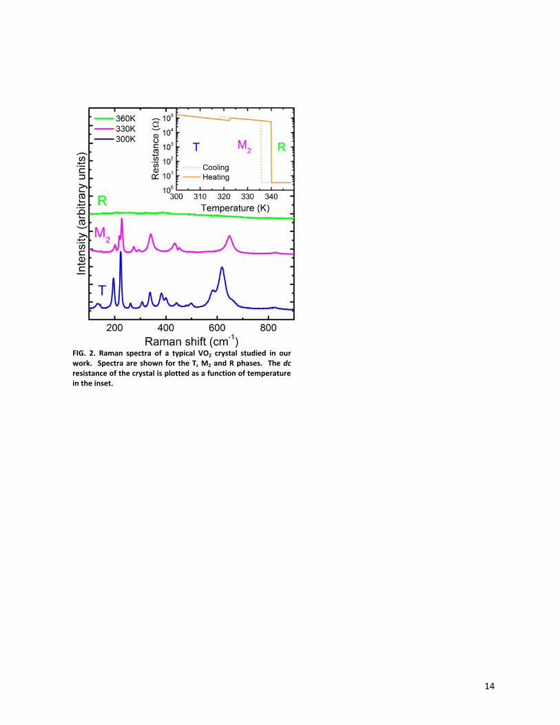
II. EXPERIMENTAL METHODS
Pure VO2 crystals were grown with a self-flux method and thoroughly characterized with
transport and X-ray diffraction measurements [29,33]. X-ray diffraction together with resistance
measurements have determined that upon heating, the crystal first goes through an insulator-to-
insulator transition and a structural transition between the T phase and the M2 phase [29,33].
The temperature dependent resistance data displayed in the inset of Fig. 2 clearly shows two
discontinuities along with hysteresis, indicative of first order phase transitions. The resistance
increases by about a factor of two upon the structural transition from the T phase to the M2
phase, consistent with previous measurements in the literature [31]. Upon further heating, the
crystal undergoes an insulator to metal transition and a structural change from the M2 phase to

5
the metallic R phase. Unpolarized Raman micro-spectroscopy on the T, M2, and R phases,
presented in Fig. 2, verifies the structural assignment from x-ray diffraction when compared to
unpolarized Raman spectra in the literature [26,34]. Our crystals are in the shape of rods with
approximately square cross-sections between 50 μm and 100 μm wide, and with lengths between
1 mm and 3 mm. The rutile cR axis, which points along the vanadium chains in the insulating
phases, is oriented along the long axis of the crystals. Through an optical microscope, we
observe that the crystal increases in length by ~ 0.6% upon transitioning from the T phase to the
M2 phase, and decreases in length by ~ 1.7 % across the MIT from M2 to R. These changes in
length are consistent with the changes in the lattice parameters along the vanadium chains
measured with x-ray diffraction in previous works [35,36]. The surface of the crystal is
identified by X-ray diffraction as the 110 plane in the rutile basis which transforms to two
coexisting, twinned surfaces 201 and 201 in the monoclinic M2 phase [37]. Further twinning
occurs as the 2-fold rotational symmetry of the M2 phase is lost upon transitioning to the T
phase. The result is that for each M2 twin, there are two possible T phase twins, which differ
from each other by a 180◦ rotation along the cR (bM2) direction [38].
The small size of the VO2 crystals calls for specialized infrared and optical micro-
spectroscopy techniques to obtain reliable data with good signal-to-noise ratio. Infrared
reflectance micro-spectroscopy between 150 and 6000 cm-1 was performed at beamline U12IR at
the National Synchrotron Light Source, Brookhaven National Laboratory [39]. Infrared
polarizers were employed to obtain reflectance spectra parallel and perpendicular to the long axis
of the crystals, i.e. the rutile cR direction. Absolute values of the infrared reflectance spectra in
the T and M2 insulating phases were obtained by normalizing them to the nearly featureless
spectra of the rutile metal.

6
Generalized spectroscopic micro-ellipsometry between 0.6 and 5.5 eV (~4800 and
~44000 cm-1) was performed at William and Mary using an in-house focusing set-up coupled to
a Woollam Variable Angle Spectroscopic Ellipsometer (W-VASE). Spectroscopic ellipsometry
has the notable advantage over reflectance spectroscopy alone in that it preserves information
related to the phase shift upon reflection, enabling the accurate determination of both the real and
imaginary parts of the optical constants of the material. Data for three angles of incidence was
obtained on the crystals oriented with their long axis parallel and perpendicular to the plane of
incidence. The same crystals and heating arrangement were used for both the reflectance and
ellipsometry experiments. All data sets were analyzed together in the W-VASE software with
Kramers-Kronig consistent oscillators to obtain the broadband, frequency dependent complex
conductivity parallel and perpendicular to the vanadium chains in the T and M2 phases.
III. RESULTS AND DISCUSSION
We present the first report on polarization dependent optical conductivity data on the
infrared-active phonons of M2 and T phases in Fig. 3. For the M2 phase (space group C2/m),
group theory predicts 6 Au phonon modes for light polarized parallel to the M axis oriented
along the vanadium chains, and 9 Bu phonon modes for light polarized perpendicular to the M
axis. We observe 5 Au and all 9 Bu phonon modes in the experimental spectra. It is possible that
the sixth Au phonon mode has a weak dipole moment and therefore is not seen in experiment.
The discontinuous structural phase transition to the T phase is captured by the significant
increase in the number of phonon features in the T spectra in both polarizations. This is
explained by the lower symmetry of the triclinic structure (space group C1 ). In Fig. 3, we
include the M1 spectra from our previous work for comparison [40]. The M1 phonon spectra
resemble the T phonon spectra and lead to the conclusion that the T phase is merely a slight

7
structural distortion of the M1 phase. Indeed this is consistent with past observation of the
continuous crossover from the M1 to the T phase without latent heat [18]. This is in contrast to
the first order phase transition between the M2 and T phases.
We now turn to the inter-band transitions in the optical conductivity that are a measure of
the electronic structure. From Fig. 4, one can immediately see that the optical conductivity, and
thus the electronic structure, of the M2 and T phases is nearly the same. This finding is
remarkable given that there are obvious differences in the structural and magnetic properties
between the two phases, as discussed above. Interestingly, numerous measurements on single
crystals and thin films of the M1 phase give almost the same magnitude of the energy gap as we
measure in the M2 and T phases [10,19–23]. The optical energy gap is the spectral region with
vanishing conductivity. Above the gap, the optical interband transition labeled Δ, is quite rigid
across this wide range of VO2 samples.
For a direct comparison to the M1 phase, in Figure 4 we show optical conductivity
extracted from the reflectance spectrum of Verleur et al. on single crystals [41]. The complex
conductivity is not uniquely determined by the reflectance intensity spectrum without knowledge
of the reflectance phase. In addition to the optical conductivity reported in Ref. [41], we present
an alternative determination of the optical conductivity using the T phase complex conductivity
measured here to approximate the value of the M1 reflectance phase shift in the high energy
region of the spectrum. Using this constraint leads to an M1 conductivity spectrum with a lower
uncertainty than that reported in the original work, where the reflectance phase shift was not
measured. The M1 optical gap is nearly the same as that in the M2 and T phases, and similar
optical interband features are present in all three phases.

8
A schematic of the effective electronic structure of the vanadium d-bands for the three
insulating VO2 phases is shown in the inset of Fig. 4 (b). There are two features of particular
note, labeled Δ and Δ||. The interband transition Δ across the energy gap is centered about 1.2 eV
for all three phases and has little polarization dependence. Similarly, Δ|| occurs around 2.5 eV in
all phases for light polarized along the vanadium chains, and is thus ascribed to transitions
between the bonding and anti-bonding a1g bands. These can be thought of as the lower and upper
Hubbard bands in the Mott picture. The features labeled Ω occur at 3 eV or higher energies and
are primarily optical interband transitions between O2p states and the empty vanadium d-states.
We emphasize that the robustness of the insulating phase band structure, despite the change in
lattice structure, is a remarkable result that is not anticipated by conventional band theory.
IV. THEORY
To investigate this behavior further, we performed ab initio hybrid DFT calculations on
the three insulating phases with the Heyd-Scuseria-Ernzerhof (HSE) functional [42,43].
Calculated optical conductivities were determined from the imaginary part of the optical
dielectric tensor, using the Vienna Ab initio Simulation Package (VASP) [44–47] with HSE
(screened) exact-exchange fraction α=0.05 and screening parameter µ=0.2. The optical
conductivity calculations are for vertical-only transitions (initial and final states are at the same
k-point). The theoretical conductivities were broadened by 0.3 eV, except as indicated, to
account for quasiparticle lifetime effects not included in HSE. With suitably chosen α, the HSE
functional can, in many instances, provide a good description of electronic properties ranging
from band to Mott-Hubbard insulators as shown in previous work [48,49]. The percentage α of
exact-change in hybrid DFT can be semi-quantitatively related to the value of the Hubbard U
parameter in DFT+U, with larger values of α (and U) yielding larger optical gaps [48–50].

9
Hybrid DFT and DFT+U both provide a mean-field treatment of on-site 3d correlation on the V
atoms. Previous M1 and M2 HSE calculations [51,52] used α=0.25 calculations, which yielded
too large band gaps, compared to experiment [53]. The results of our hybrid DFT calculations
are presented in Fig. 4 (c) and (d). In agreement with the experiment, we find that the energy
values of the inter-band transitions, particularly Δ across the optical gap, are quite similar for all
three phases. DFT+U calculations (U=5.7 eV and J=0.8 eV, using LDAUTYPE=1 in VASP, not
shown) yield qualitatively similar results. This insensitivity to the change in lattice structure in
all three insulating phases is incompatible with the Peierls picture. It is interesting to note that the
Δ|| feature in the raw HSE result is much sharper than in experiment (see Fig. 4). This is
indicative of short lifetimes for carriers excited between the bonding and anti-bonding a1g bands
in the real system that is not captured in the static HSE theory. Such lifetime broadening is
characteristic of significant electron-electron interactions in these orbitals of Mott-Hubbard
character. This is additional evidence that the splitting of the a1g bands, and consequently the
energy gap, arises from Coulomb correlations. The most recent iteration of DMFT electronic
structure calculations finds energy gaps for the M1 and M2 phases that are consistent with our
experimental results [54].
V. CONCLUSIONS
To conclude, the nature of the VO2 insulating phases is now clear. The optical
spectroscopy data presented in this work clearly demonstrates that the electronic structure of the
VO2 insulating phases is robust to changes in lattice structure and vanadium-vanadium pairing.
In particular, the energy gap is insensitive to the dimerization of the equally spaced vanadium
ions with localized electrons in the M2 chains. This result is incompatible with a Peierls gap and
is strong evidence that the gap arises due to Mott-Hubbard type Coulomb correlations. The

10
negative Knight shift is indicative of localized electrons on the equally spaced vanadium ions in
the M2 chains. Its absence in the dimerized chains of all three phases [18] elucidates the key
subtlety of the insulating VO2 states: in contrast to a more conventional Mott insulator, where
valence electrons are localized on individual ions, the dimerized vanadium chains contain
bonded spin singlets which are localized on the vanadium dimers. This fact has made it difficult
to conclusively distinguish between the Peierls and Mott-Hubbard pictures in the exhaustively
studied M1 phase. Study of the M2 and T phases, with their non-equal V chains, is essential to
decouple the effects of dimerization and electronic correlations. Seen in a broader context, our
work paves a path for disentangling the contributions of the electronic and structural degrees of
freedom to phase transitions in other correlated electron systems.
ACKNOWLEDGMENTS
MMQ acknowledges financial support from NSF DMR (grant # 1255156) and the
Jeffress Memorial Trust (grant # J-1014). HK acknowledges support from ONR (grant
N000141211042) and from the computational facilities at the College of William and Mary. HJ
acknowledges support from National Research Foundation of Korea (NRF-
2015R1D1A1A01059297). The authors thank Dr. Nobumichi Tamura for discussions on the
assignment of twins in the M2 and T phases based on the x-ray diffraction data.
* Corresponding author email address: [email protected]
[1] M. Imada, A. Fujimori, and Y. Tokura, Rev. Mod. Phys. 70, 1039 (1998). [2] A. Perucchi, L. Baldassarre, P. Postorino, and S. Lupi, J. Physics-Condensed Matter 21,
323202 (2009). [3] D. N. Basov, R. D. Averitt, D. van der Marel, M. Dressel, and K. Haule, Rev. Mod. Phys.

11
83, 471 (2011). [4] A. X. Gray, J. Jeong, N. P. Aetukuri, P. Granitzka, Z. Chen, R. Kukreja, D. Higley, T.
Chase, A. H. Reid, H. Ohldag, M. A. Marcus, A. Scholl, A. T. Young, A. Doran, C. A. Jenkins, P. Shafer, E. Arenholz, M. G. Samant, S. S. P. Parkin, and H. A. D??rr, Phys. Rev. Lett. 116, 116403 (2016).
[5] J. D. Budai, J. Hong, M. E. Manley, E. D. Specht, C. W. Li, J. Z. Tischler, D. L. Abernathy, A. H. Said, B. M. Leu, L. A. Boatner, R. J. McQueeney, and O. Delaire, Nature 515, 535 (2014).
[6] J. Tomczak and S. Biermann, Phys. Rev. B 80, 85117 (2009). [7] C. Weber, D. D. O'Regan, N. D. M. Hine, M. C. Payne, G. Kotliar, and P. B. Littlewood,
Phys. Rev. Lett. 108, 256402 (2012). [8] M. Gatti, F. Sottile, and L. Reining, Phys. Rev. B 91, 195137 (2015). [9] H. Zheng and L. K. Wagner, Phys. Rev. Lett. 114, (2015). [10] T. C. Koethe, Z. Hu, M. W. Haverkort, C. Schüßler-Langeheine, F. Venturini, N. B.
Brookes, O. Tjernberg, W. Reichelt, H. H. Hsieh, H.-J. Lin, C. T. Chen, and L. H. Tjeng, Phys. Rev. Lett. 97, 116402 (2006).
[11] R. Eguchi, M. Taguchi, M. Matsunami, K. Horiba, K. Yamamoto, Y. Ishida, A. Chainani, Y. Takata, M. Yabashi, D. Miwa, Y. Nishino, K. Tamasaku, T. Ishikawa, Y. Senba, H. Ohashi, Y. Muraoka, Z. Hiroi, and S. Shin, Phys. Rev. B - Condens. Matter Mater. Phys. 78, 1 (2008).
[12] M. W. Haverkort, Z. Hu, A. Tanaka, W. Reichelt, S. V Streltsov, M. A. Korotin, V. I. Anisimov, H. H. Hsieh, H. J. Lin, C. T. Chen, D. I. Khomskii, and L. H. Tjeng, Phys. Rev. Lett. 95, 196404 (2005).
[13] V. R. Morrison, R. P. Chatelain, K. L. Tiwari, A. Hendaoui, A. Bruhács, M. Chaker, and B. J. Siwick, Science (80-. ). 346, 445 (2014).
[14] D. Wegkamp, M. Herzog, L. Xian, M. Gatti, P. Cudazzo, C. L. McGahan, R. E. Marvel, R. F. Haglund, A. Rubio, M. Wolf, and J. Stähler, Phys. Rev. Lett. 113, 2 (2014).
[15] B. T. O’Callahan, A. C. Jones, J. Hyung Park, D. H. Cobden, J. M. Atkin, and M. B. Raschke, Nat. Commun. 6, 6849 (2015).
[16] D. Wegkamp and J. Stähler, Prog. Surf. Sci. 90, 464 (2015). [17] B. Mayer, C. Schmidt, A. Grupp, J. Bühler, J. Oelmann, R. E. Marvel, R. F. Haglund, T.
Oka, D. Brida, A. Leitenstorfer, and A. Pashkin, Phys. Rev. B 91, 235113 (2015). [18] J. P. Pouget, H. Launois, T. M. Rice, P. Dernier, A. Gossard, Villeneu.G, and
Hagenmul.P, Phys. Rev. B 10, 1801 (1974). [19] K. Okazaki, S. Sugai, Y. Muraoka, and Z. Hiroi, Phys. Rev. B 73, 165116 (2006). [20] M. M. Qazilbash, M. Brehm, B.-G. Chae, P.-C. Ho, G. O. Andreev, B.-J. Kim, S. J. Yun,
A. V Balatsky, M. B. Maple, F. Keilmann, H.-T. Kim, and D. N. Basov, Science (80-. ). 318, 1750 (2007).
[21] M. M. Qazilbash, A. A. Schafgans, K. S. Burch, S. J. Yun, B. G. Chae, B. J. Kim, H. T. Kim, and D. N. Basov, Phys. Rev. B 77, 115121 (2008).
12
[22] T. J. Huffman, P. Xu, A. J. Hollingshad, M. M. Qazilbash, L. Wang, R. A. Lukaszew, S. Kittiwatanakul, J. Lu, and S. A. Wolf, Phys. Rev. B 91, 205140 (2015).
[23] M. Nazari, Y. Zhao, V. V. Kuryatkov, Z. Y. Fan, A. A. Bernussi, and M. Holtz, Phys. Rev. B 87, 35142 (2013).
[24] M. Ghedira, J. Chenavas, and M. Marezio, J. Phys. C-Solid State Phys. 10, L309 (1977). [25] T. Kong, M. W. Masters, S. L. Bud’ko, and P. C. Canfield, APL Mater. 3, 41502 (2015). [26] E. Strelcov, A. Tselev, I. Ivanov, J. D. Budai, J. Zhang, J. Z. Tischler, I. Kravchenko, S. V
Kalinin, and A. Kolmakov, Nano Lett. 12, 6198 (2012). [27] J. P. Pouget, H. Launois, J. P. Dhaenens, P. Merenda, and T. M. Rice, Phys. Rev. Lett. 35,
873 (1975). [28] J. P. Dhaenens, D. Kaplan, and P. Merenda, J. Phys. C-Solid State Phys. 8, 2267 (1975). [29] B. S. Mun, K. Chen, Y. Leem, C. Dejoie, N. Tamura, M. Kunz, Z. Liu, M. E. Grass, C.
Park, J. Yoon, Y. Y. Lee, and H. Ju, Phys. Status Solidi - Rapid Res. Lett. 5, 107 (2011). [30] B. S. Mun, K. Chen, J. Yoon, C. Dejoie, N. Tamura, M. Kunz, Z. Liu, M. E. Grass, S.-K.
Mo, C. Park, Y. Y. Lee, and H. Ju, Phys. Rev. B 84, 113109 (2011). [31] M. Ghedira, H. Vincent, M. Marezio, and J. C. Launay, J. Solid State Chem. 22, 423
(1977). [32] T. M. Rice, H. Launois, and J. P. Pouget, Phys. Rev. Lett. 73, 3042 (1994). [33] B. S. Mun, K. Chen, Y. Leem, C. Dejoie, N. Tamura, M. Kunz, Z. Liu, M. E. Grass, C.
Park, J. Yoon, Y. Y. Lee, and H. Ju, Phys. Status Solidi - Rapid Res. Lett. 9, 206 (2015). [34] C. Marini, E. Arcangeletti, D. Di Castro, L. Baldassare, a. Perucchi, S. Lupi, L. Malavasi,
L. Boeri, E. Pomjakushina, K. Conder, and P. Postorino, Phys. Rev. B 77, 235111 (2008). [35] M. Marezio, B. Mcwhan, P. D. Dernier, and J. P. Remeika, Phys. Rev. B-Solid State 5,
2541 (1972). [36] J. Cao, Y. Gu, W. Fan, L. Q. Chen, D. F. Ogletree, K. Chen, N. Tamura, M. Kunz, C.
Barrett, J. Seidel, and J. Wu, Nano Lett. 10, 2667 (2010). [37] J. Cao, Y. Gu, W. Fan, L. Q. Chen, D. F. Ogletree, K. Chen, N. Tamura, M. Kunz, C.
Barrett, J. Seidel, and J. Wu, Nano Lett. 10, 2667 (2010). [38] M. Marezio, Acta Crystallogr. 29, 618 (1973). [39] G. L. Carr, Rev. Sci. Instrum. 72, 1613 (2001). [40] T. Huffman, P. Xu, M. Qazilbash, E. Walter, H. Krakauer, J. Wei, D. Cobden, H. Bechtel,
M. Martin, G. Carr, and D. Basov, Phys. Rev. B 87, 115121 (2013). [41] H. W. Verleur, A. S. Barker, and C. N. Berglund, Phys. Rev. 172, 788 (1968). [42] J. Heyd, G. E. Scuseria, and M. Ernzerhof, J. Chem. Phys. 118, 8207 (2003). [43] J. Heyd, G. E. Scuseria, and M. Ernzerhof, J. Chem. Phys. 124, (2006). [44] G. Kresse and J. Hafner, Phys. Rev. B 47, 558 (1993). [45] G. Kresse and J. Furthmuller, Phys. Rev. B 54, 11169 (1996). [46] G. Kresse and J. Furthmuller, Comput. Mater. Sci. 6, 15 (1996).

13
[47] G. Kresse and D. Joubert, Phys. Rev. B 59, 1758 (1999). [48] J. He and C. Franchini, Phys. Rev. B 86, 235117 (2012). [49] C. Franchini, J. PHYSICS-CONDENSED MATTER 26, 235202 (2014). [50] V. Ivady, R. Armiento, K. Szasz, E. Janzen, A. Gali, and I. A. Abrikosov, Phys. Rev. B
90, (2014). [51] V. Eyert, Phys. Rev. Lett. 107, 16401 (2011). [52] N. F. Quackenbush, H. Paik, M. J. Wahila, S. Sallis, M. E. Holtz, X. Huang, A. Ganose,
B. J. Morgan, D. O. Scanlon, Y. Gu, F. Xue, L.-Q. Chen, G. E. Sterbinsky, C. Schlueter, T.-L. Lee, J. C. Woicik, J.-H. Guo, J. D. Brock, D. A. Muller, D. A. Arena, D. G. Schlom, and L. F. J. Piper, Phys. Rev. B 94, 85105 (2016).
[53] Eyert's 2011 PRL (Ref. [51]) references both Heyd al. 2003 and 2006 (Refs. [42,43]). While not made explicit, we assume Eyert used HSE06, which sets α=0.25.
[54] W. H. Brito, M. C. O. Aguiar, K. Haule, and G. Kotliar, Phys. Rev. Lett. 117, 56402 (2016).
FIG. 1. A plan view of vanadium ion positions for the metallic rutile and insulating M2, T, and M1 phases of VO2. In all phases, the vanadium ions at the center of each rutile unit cell (shown by the gridlines) are offset from the others by ½ unit cell (denoted by “1/2” in the rutile panel). The vanadium ions in the insulating phases undergo small displacements from the rutile positions (open green circles in the panels of the insulating phases). The rutile lattice vectors cR and aR are shown in the lower left corner of the diagram. Vanadium chains in the insulating phases are oriented along the cR direction.
14
FIG. 2. Raman spectra of a typical VO2 crystal studied in our work. Spectra are shown for the T, M2 and R phases. The dc resistance of the crystal is plotted as a function of temperature in the inset.

15
FIG. 3. Polarization dependent optical conductivity (σ1) showing the infrared active phonon spectra of the M2 phase (panels (a) and (b)), and the T phase (panels (c) and (d)). The center frequencies of the phonon features are denoted by circles labeled νcenter. The previously reported M1 phase infrared active phonon spectra [40] are compared to the triclinic phase spectra in (c) and (d).

16
FIG. 4. Experimental optical conductivity σ1 of the M2 and triclinic T phases parallel to the vanadium (V) chains (a) andperpendicular to the vanadium (V) chains (b). Phonon features, which occur below 0.11 eV, are not shown. For comparison,accurate optical conductivity of the M1 phase is extracted from the reflectance spectrum reported in [41] by using the complexconductivity of the T phase measured in this work as a constraint above 4 eV (see text). The inset in panel (b) shows an effectiveenergy level diagram along with optical interband transitions that appear in the conductivity spectra. First-principles DFT opticalconductivities calculated via the HSE functional are presented in (c) and (d). The calculated “raw” conductivities are broadened by0.3 eV. The calculated conductivity for Ellcr contains a very sharp Δll feature (see inset of panel (c)). To account for lifetime effectsnot handled in the static HSE treatment, the Δll feature, which is assigned to transitions between the lower and upper Hubbardbands in the Mott picture, is further broadened to a FWHM of 1.5 eV in the main panel of (c), which better models theexperiment.