InSb-Based Heterostructures for Electronic Device Applications
30
InSb-Based Heterostructures for Electronic Device Applications Michael Santos Homer L. Dodge Department of Physics & Astronomy University of Oklahoma Norman, OK 73019 USA Funded by NSF DMR-0808086 and DMR-0520550
Transcript of InSb-Based Heterostructures for Electronic Device Applications
InSb-Based Heterostructures for Electronic Device Applications
Michael Santos Homer L. Dodge Department of Physics & Astronomy
University of OklahomaNorman, OK 73019 USA
Funded by NSF DMR-0808086 and DMR-0520550
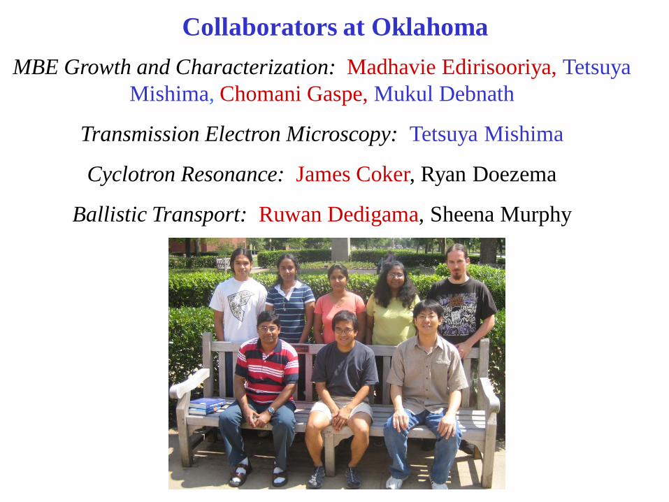
Collaborators at OklahomaMBE Growth and Characterization: Madhavie Edirisooriya, Tetsuya
Mishima, Chomani Gaspe, Mukul Debnath
Transmission Electron Microscopy: Tetsuya Mishima
Cyclotron Resonance: James Coker, Ryan Doezema
Ballistic Transport: Ruwan Dedigama, Sheena Murphy
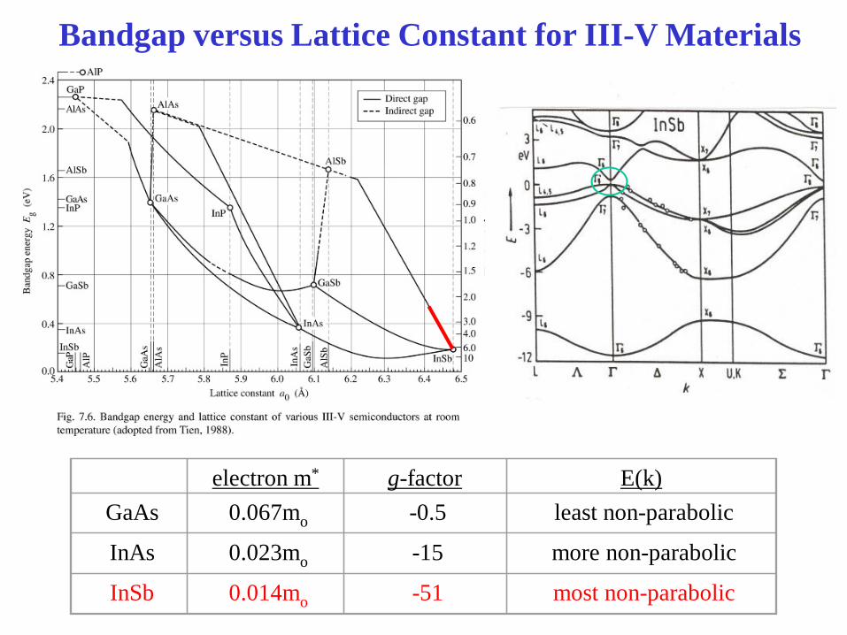
Bandgap versus Lattice Constant for III-V Materials
electron m* g-factor E(k)GaAs 0.067mo -0.5 least non-parabolic
InAs 0.023mo -15 more non-parabolic
InSb 0.014mo -51 most non-parabolic
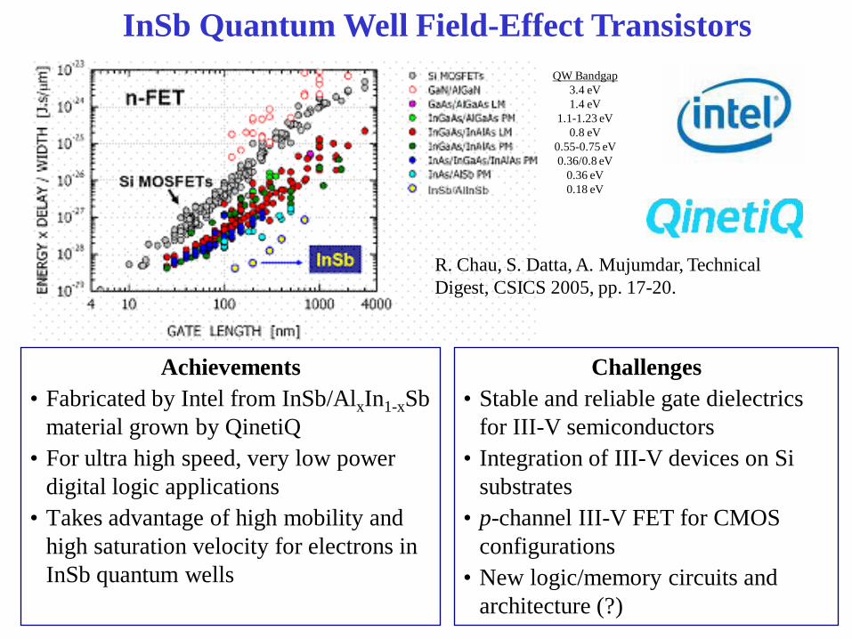
R. Chau, S. Datta, A. Mujumdar, Technical Digest, CSICS 2005, pp. 17-20.
QW Bandgap3.4 eV1.4 eV
1.1-1.23 eV0.8 eV
0.55-0.75 eV0.36/0.8 eV
0.36 eV0.18 eV
Achievements• Fabricated by Intel from InSb/AlxIn1-xSb
material grown by QinetiQ• For ultra high speed, very low power
digital logic applications• Takes advantage of high mobility and
high saturation velocity for electrons in InSb quantum wells
InSb Quantum Well Field-Effect Transistors
Challenges• Stable and reliable gate dielectrics
for III-V semiconductors• Integration of III-V devices on Si
substrates• p-channel III-V FET for CMOS
configurations• New logic/memory circuits and
architecture (?)
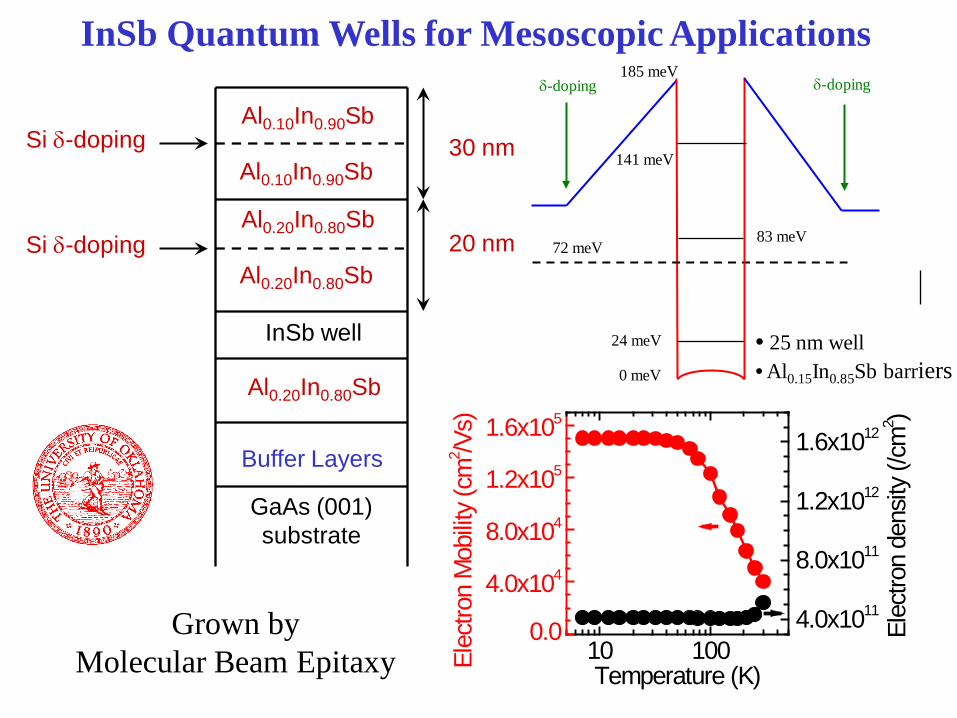
Al0.10In0.90Sb
Al0.10In0.90Sb
Al0.20In0.80Sb
Al0.20In0.80Sb
Al0.20In0.80Sb
InSb well
Buffer Layers
GaAs (001) substrate
30 nm
20 nmSi δ-doping
Si δ-doping
InSb Quantum Wells for Mesoscopic Applicationsδ-doping
24 meV
0 meV
83 meV72 meV
δ-doping185 meV
141 meV
• 25 nm well • Al0.15In0.85Sb barriers
10 1000.0
4.0x10⁴
8.0x10⁴
1.2x10⁵
1.6x10⁵
4.0x10¹¹
8.0x10¹¹
1.2x10¹²
1.6x10¹²
Elec
tron
Mob
ility
(cm
2 /Vs)
Temperature (K)
Ele
ctro
n de
nsity
(/cm
2 )
Grown by Molecular Beam Epitaxy

Outline1. Introduction
2. Transmission Electron Microscopy• Effect of Crystalline Defects on Electron Mobility• Effect of Buffer Layer on Defect Densities
3. Transport Experiments on 2D Electron Systems• Quantum Hall Effect• Quantized Conductance in Wires• Magnetic Focusing
4. Realization of 2D Hole Systems• Transport properties• Cyclotron resonance
5. Summary
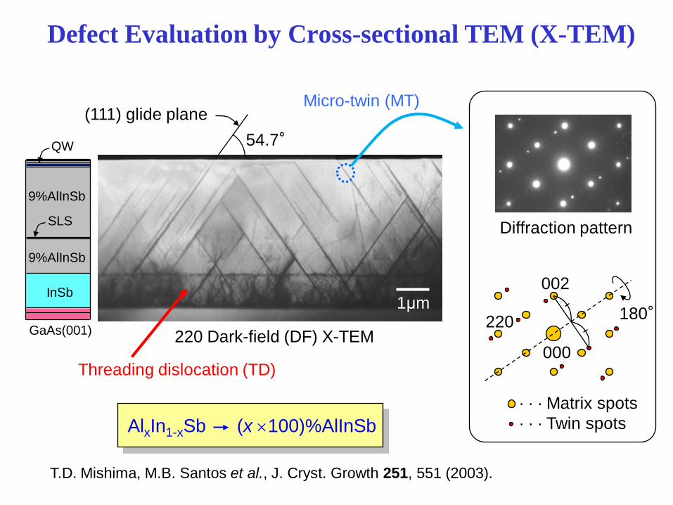
Defect Evaluation by Cross-sectional TEM (X-TEM)
54.7°
(111) glide plane
1μm
· · · Matrix spots· · · Twin spots
000
002
220 180°
Diffraction pattern
InSb
9%AlInSb
9%AlInSb
GaAs(001)
Threading dislocation (TD)
QW
SLS
Micro-twin (MT)
220 Dark-field (DF) X-TEM
T.D. Mishima, M.B. Santos et al., J. Cryst. Growth 251, 551 (2003).
AlxIn1-xSb (x ×100)%AlInSb
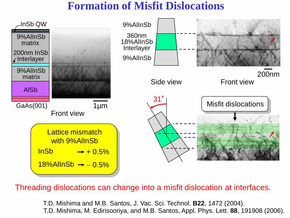
Formation of Misfit Dislocations
360nm18%AlInSbInterlayer
9%AlInSb
9%AlInSb
31°
Front view
Misfit dislocations
200nmSide view
Threading dislocations can change into a misfit dislocation at interfaces.
1µmFront view
200nm InSbInterlayer
AlSb
9%AlInSbmatrix
9%AlInSbmatrix
InSb QW
GaAs(001)
Lattice mismatchwith 9%AlInSb
InSb
18%AlInSb
+ 0.5%
− 0.5%
T.D. Mishima, M. Edirisooriya, and M.B. Santos, Appl. Phys. Lett. 88, 191908 (2006).T.D. Mishima and M.B. Santos, J. Vac. Sci. Technol. B22, 1472 (2004).
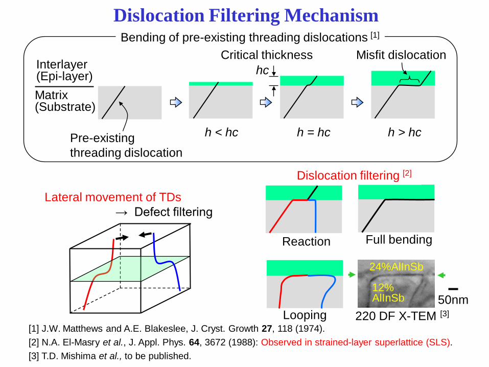
Dislocation Filtering Mechanism
[1] J.W. Matthews and A.E. Blakeslee, J. Cryst. Growth 27, 118 (1974).[2] N.A. El-Masry et al., J. Appl. Phys. 64, 3672 (1988): Observed in strained-layer superlattice (SLS).[3] T.D. Mishima et al., to be published.
50nm
24%AlInSb
12%AlInSb
Dislocation filtering [2]
Full bending
Looping
Reaction
220 DF X-TEM [3]
Lateral movement of TDs→ Defect filtering
Pre-existingthreading dislocation
Matrix(Substrate)
Interlayer(Epi-layer) hc
h < hc h = hc h > hc
Critical thickness Misfit dislocationBending of pre-existing threading dislocations [1]
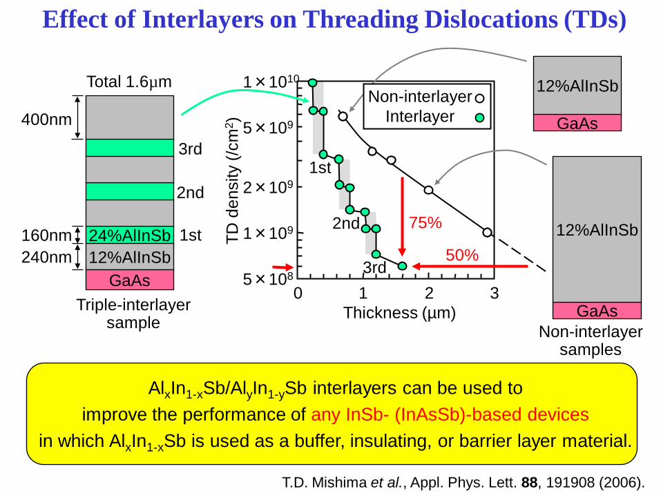
Effect of Interlayers on Threading Dislocations (TDs)
10 2 3Thickness (µm)
TD d
ensi
ty (/
cm2 )
5×10⁸
1×10⁹
2×10⁹
5×10⁹
1×10¹⁰
1st
2nd
3rd
GaAs
12%AlInSb
GaAs
12%AlInSb
240nm160nm 1st
2nd
3rd
75%
50%
Triple-interlayersample Non-interlayer
samples
Total 1.6µm
24%AlInSb12%AlInSb
GaAs
400nm
T.D. Mishima et al., Appl. Phys. Lett. 88, 191908 (2006).
Non-interlayerInterlayer
AlxIn1-xSb/AlyIn1-ySb interlayers can be used to improve the performance of any InSb- (InAsSb)-based devices
in which AlxIn1-xSb is used as a buffer, insulating, or barrier layer material.
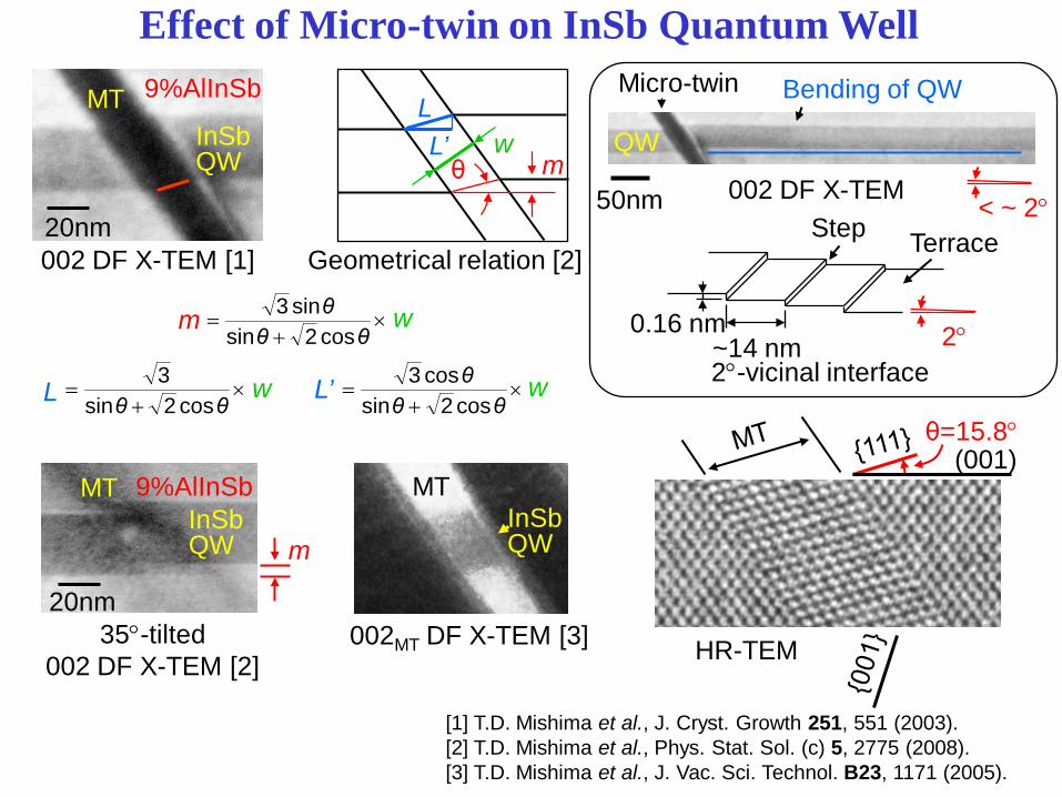
Effect of Micro-twin on InSb Quantum Well
wθθ
θm ×+
=cos2sin
sin3
50nm
QW
< ~ 2°
~14 nm0.16 nm 2°
20nm
m
9%AlInSb
mL’
L9%AlInSb
w
20nm
InSbQW
wθθ
θL ×+
=cos2sin
cos3'wθθ
L ×+
=cos2sin
3
θ=15.8°(001)
InSbQW
InSbQW
θ
[1] T.D. Mishima et al., J. Cryst. Growth 251, 551 (2003).[2] T.D. Mishima et al., Phys. Stat. Sol. (c) 5, 2775 (2008).[3] T.D. Mishima et al., J. Vac. Sci. Technol. B23, 1171 (2005).
m w
ww L’L
Micro-twin
002 DF X-TEMStep Terrace
2°-vicinal interface
Bending of QW
HR-TEM
002 DF X-TEM [1] Geometrical relation [2]
MT
002MT DF X-TEM [3]
MT MT
35°-tilted 002 DF X-TEM [2]
Electron Mobility and Structural Defects
4×10⁴
3×10⁴
2×10⁴
0
3.6×10⁹
0
1.2×1046×103
1.8×10⁹
10 1000.0
4.0x10⁴
8.0x10⁴
1.2x10⁵
1.6x10⁵
4.0x10¹¹
8.0x10¹¹
1.2x10¹²
1.6x10¹²
Elec
tron
Mob
ility
(cm
2 /Vs)
Temperature (K)
Ele
ctro
n de
nsity
(/cm
2 )
Hal
l Mob
ility
(cm
2 /Vs)
Car
rier D
ensi
ty(/c
m2 )
T.D. Mishima et al., Appl. Phys. Lett. 91, 062106 (2007).
Electron Mobility in InSb QW @RT30,000 41,000 cm2/Vs (37%↑)
(n = 5.5×10¹¹/cm2)
Temperature (K)
MT density980 /cm
7,600 /cmOn-axis GaAs(001)[ tQW = 20nm ]
2° off-cut GaAs(001)[ tQW = 20nm ]
2° off-cut GaAs(001)[ tQW = 25nm ]
Summary of Defect Studies
• Mobility partially limited by threading dislocations and micro-twin defects
• Threading dislocations reduced by interlayers in the buffer layer
• Micro-twin density reduced by growth on off-axis substrates
Outline1. Introduction
2. Transmission Electron Microscopy• Effect of Crystalline Defects on Electron Mobility• Effect of Buffer Layer on Defect Densities
3. Transport Experiments on 2D Electron Systems• Quantum Hall Effect• Quantized Conductance in Wires• Magnetic Focusing
4. Realization of 2D Hole Systems• Transport properties• Cyclotron resonance
5. Summary
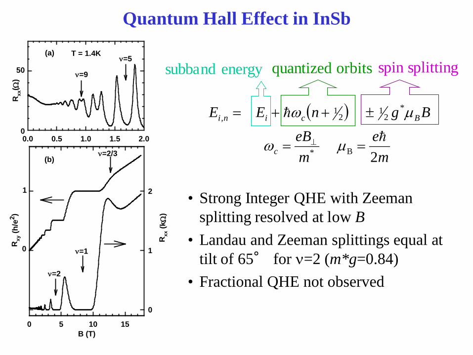
0.0 0.5 1.0 1.5 2.0
Rxx
( Ω)
B (T)0 5 10 15
Rxy
(h/e
2 )
Rxx
(kΩ
)
0
1
2
ν=1
ν=2
ν=2/3
0
1
(b)
50
0
T = 1.4K(a)ν=5
ν=9
Quantum Hall Effect in InSb
( )
me
meB
BgnEE
c
Bcini
2
B*
*2
12
1,
==
±++=
⊥ µω
µω
quantized orbits spin splittingsubband energy
• Strong Integer QHE with Zeeman splitting resolved at low B
• Landau and Zeeman splittings equal at tilt of 65° for ν=2 (m*g=0.84)
• Fractional QHE not observed
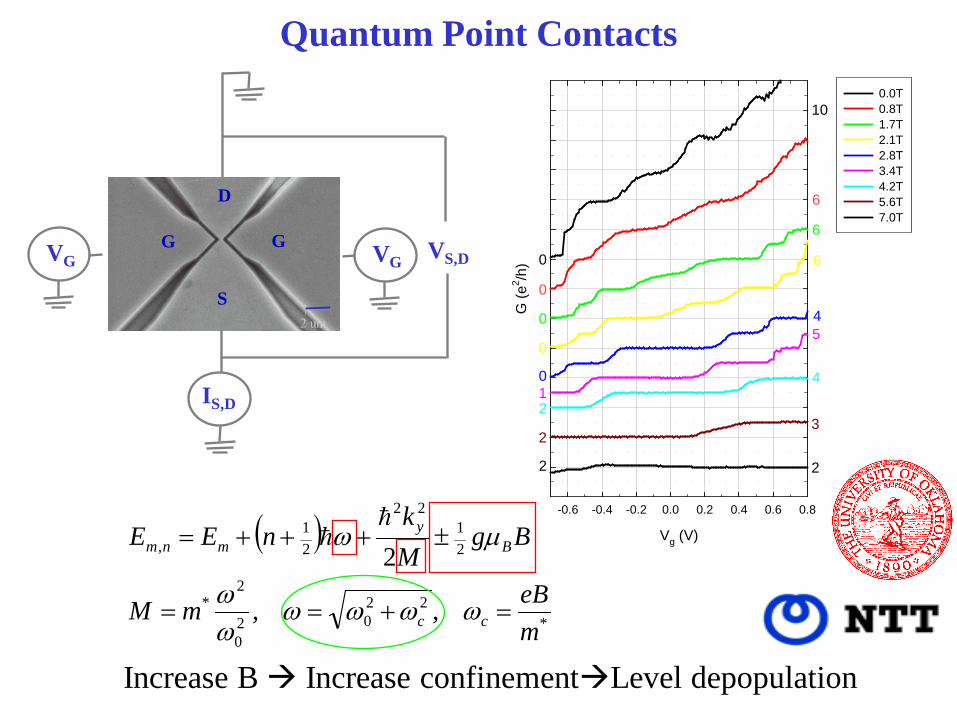
Vg (V)
-0.6 -0.4 -0.2 0.0 0.2 0.4 0.6 0.8G
(e2 /h
)
0.0T0.8T1.7T2.1T2.8T3.4T4.2T5.6T7.0T
0
0
0
0
012
23
4
54
6
6
6
10
2 2
Quantum Point Contacts
Increase B Increase confinementLevel depopulation
( )
*22
020
2*
21
22
21
,
,,
2
meBmM
BgMk
nEE
cc
By
mnm
=+==
±+++=
ωωωωωω
µω
VS,D
D
G G
S
IS,D
VGVG
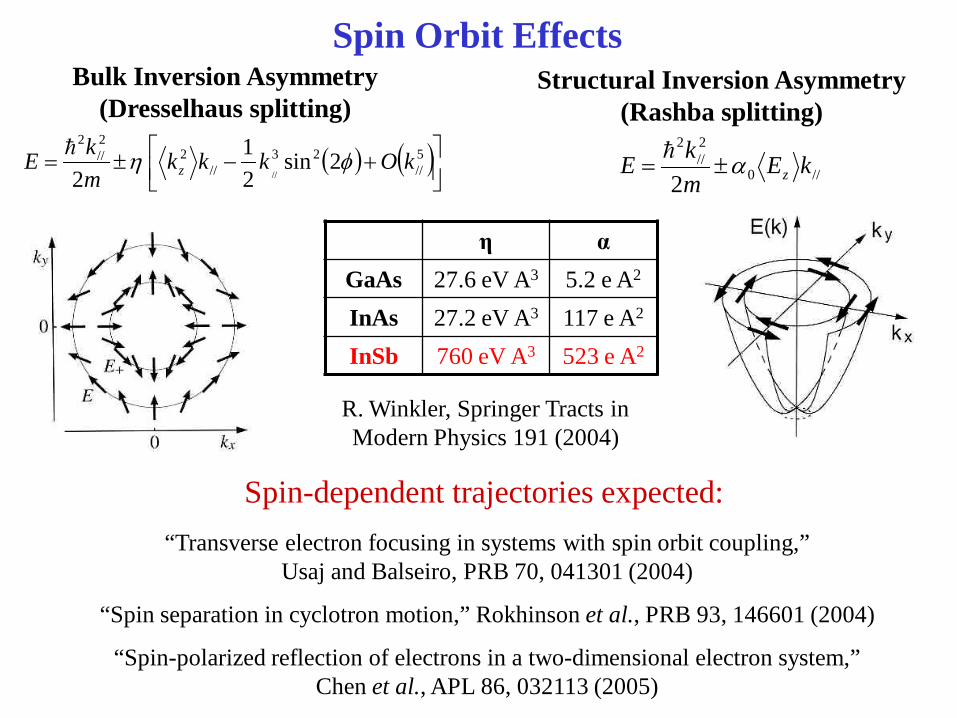
Spin Orbit Effects
η αGaAs 27.6 eV A3 5.2 e A2
InAs 27.2 eV A3 117 e A2
InSb 760 eV A3 523 e A2
R. Winkler, Springer Tracts in Modern Physics 191 (2004)
Bulk Inversion Asymmetry (Dresselhaus splitting)
Structural Inversion Asymmetry(Rashba splitting)
“Transverse electron focusing in systems with spin orbit coupling,” Usaj and Balseiro, PRB 70, 041301 (2004)
“Spin separation in cyclotron motion,” Rokhinson et al., PRB 93, 146601 (2004)
“Spin-polarized reflection of electrons in a two-dimensional electron system,” Chen et al., APL 86, 032113 (2005)
//0
2//
2
2kE
mkE zα±=
( ) ( )
+−±= 5
//23
//2
2//
2
2sin21
2 //kOkkk
mkE z φη
Spin-dependent trajectories expected:
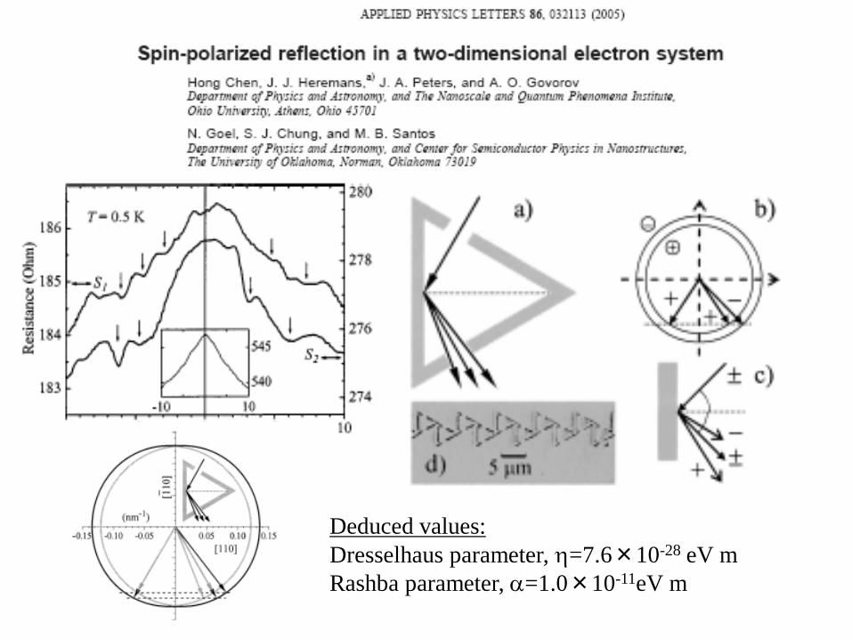
Deduced values:Dresselhaus parameter, η=7.6×10⁻²⁸ eV mRashba parameter, α=1.0×10⁻¹¹eV m
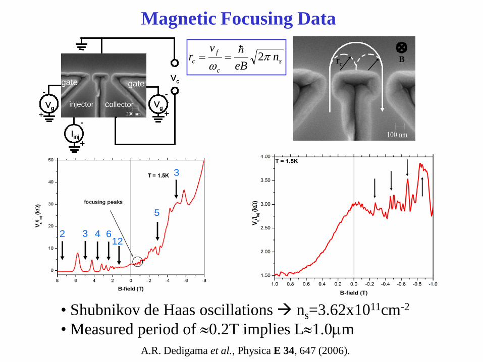
Magnetic Focusing Data
2 3 4 612
3
5
2 3 4 612
3
5
injector
gategate
collector
Vc
Iinj
-
+
Vg Vg
--
++injector
gategate
collector
Vc
Iinj
-
+
Vg Vg
--
+injector
gategate
collector
Vc
Iinj
-
+
Vg Vg
--
++
• Shubnikov de Haas oscillations ns=3.62x1011cm-2
• Measured period of ≈0.2T implies L≈1.0µm
rc Brcrc Bsc
fc n
eBv
r πω
2==
A.R. Dedigama et al., Physica E 34, 647 (2006).
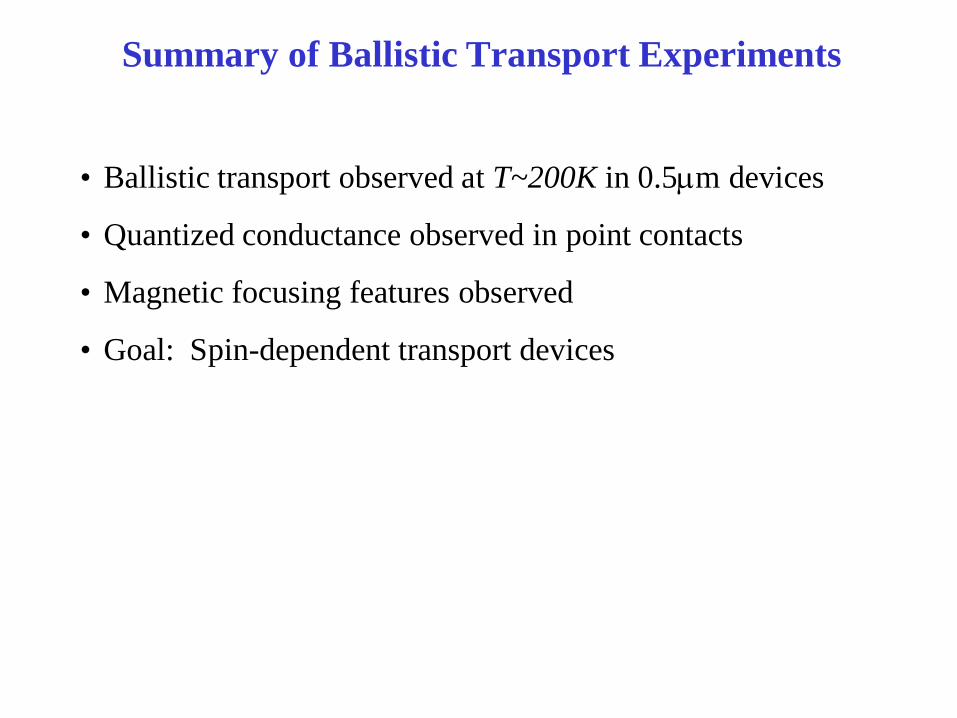
Summary of Ballistic Transport Experiments
• Ballistic transport observed at T~200K in 0.5µm devices
• Quantized conductance observed in point contacts
• Magnetic focusing features observed
• Goal: Spin-dependent transport devices

Outline1. Introduction
2. Transmission Electron Microscopy• Effect of Crystalline Defects on Electron Mobility• Effect of Buffer Layer on Defect Densities
3. Transport Experiments on 2D Electron Systems• Quantum Hall Effect• Quantized Conductance in Wires• Magnetic Focusing
4. Realization of 2D Hole Systems• Transport properties• Cyclotron resonance
5. Summary
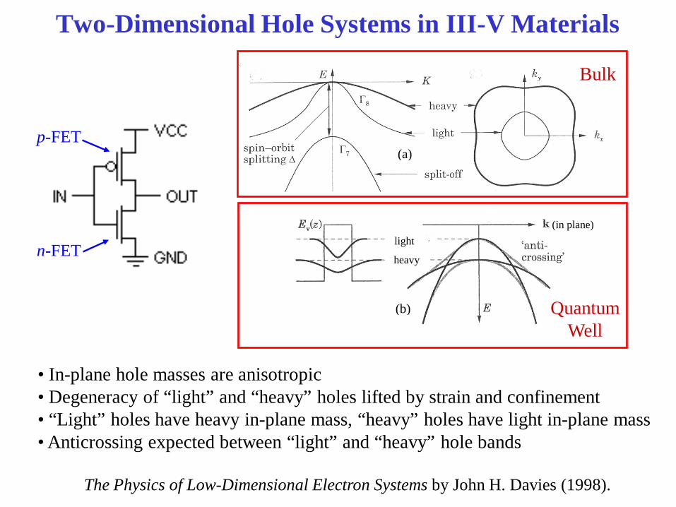
heavy
light
(b)
(a)
(in plane)
The Physics of Low-Dimensional Electron Systems by John H. Davies (1998).
• In-plane hole masses are anisotropic• Degeneracy of “light” and “heavy” holes lifted by strain and confinement• “Light” holes have heavy in-plane mass, “heavy” holes have light in-plane mass• Anticrossing expected between “light” and “heavy” hole bands
Bulk
QuantumWell
Two-Dimensional Hole Systems in III-V Materials
p-FET
n-FET
p-type InSb Quantum Well
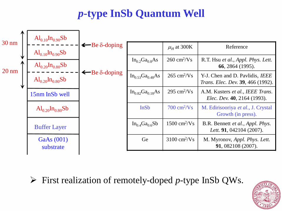
µH at 300K Reference
In0.2Ga0.8As 260 cm2/Vs R.T. Hsu et al., Appl. Phys. Lett. 66, 2864 (1995).
In0.53Ga0.48As 265 cm2/Vs Y-J. Chen and D. Pavlidis, IEEE Trans. Elec. Dev. 39, 466 (1992).
In0.82Ga0.18As 295 cm2/Vs A.M. Kusters et al., IEEE Trans. Elec. Dev. 40, 2164 (1993).
InSb 700 cm2/Vs M. Edirisooriya et al., J. Crystal Growth (in press).
In0.4Ga0.6Sb 1500 cm2/Vs B.R. Bennett et al., Appl. Phys. Lett. 91, 042104 (2007).
Ge 3100 cm2/Vs M. Myronov, Appl. Phys. Lett. 91, 082108 (2007).
Al0.10In0.90Sb
Al0.10In0.90Sb
Al0.20In0.80Sb
Al0.20In0.80Sb
Al0.20In0.80Sb
15nm InSb well
Buffer Layer
GaAs (001) substrate
30 nm
20 nm
Be δ-doping
Be δ-doping
First realization of remotely-doped p-type InSb QWs.
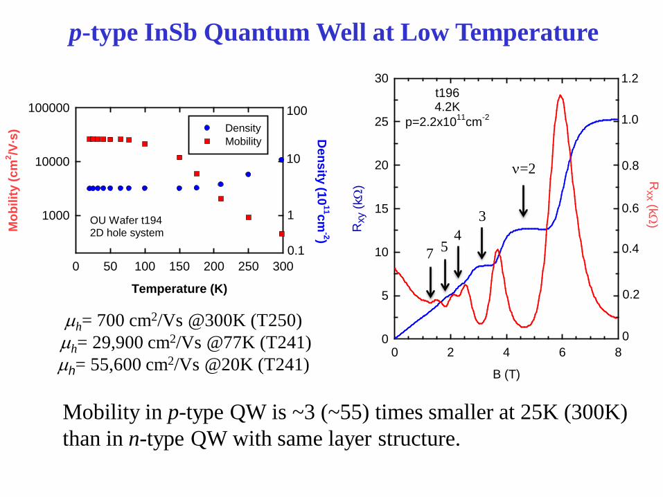
t1964.2K
p=2.2x1011cm-2
B (T)
0 2 4 6 8R
xy (k
Ω)
0
5
10
15
20
25
30
0
0.4
0.6
0.8
1.0
0.2
Rxx (kΩ
)
1.2
ν=2
34
7
p-type InSb Quantum Well at Low Temperature
Mobility in p-type QW is ~3 (~55) times smaller at 25K (300K) than in n-type QW with same layer structure.
Temperature (K)
0 50 100 150 200 250 300
Mob
ility
(cm
2 /V. s
)
1000
10000
100000DensityMobility
1
0.1
10
100
Density (10
11cm-2)
OU Wafer t1942D hole system
µh= 700 cm2/Vs @300K (T250)µh= 29,900 cm2/Vs @77K (T241)µh= 55,600 cm2/Vs @20K (T241)
5
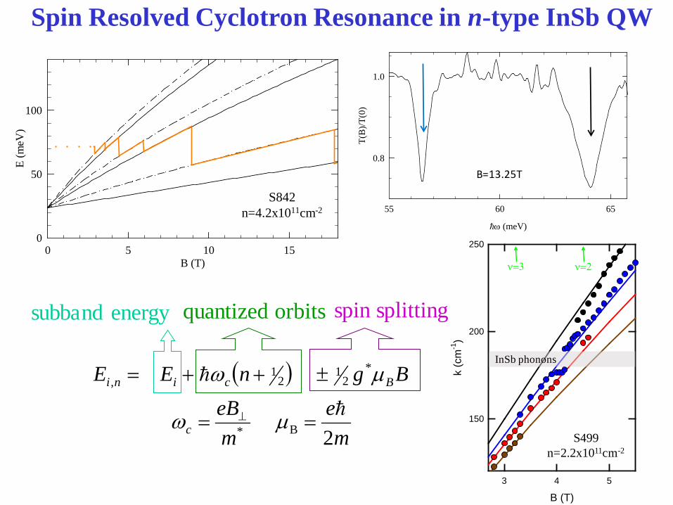
B (T)3 4 5
k (c
m-1
)
150
200
250
InSb phonons
ν=2ν=3
S499n=2.2x1011cm-2
n=0
n=1n=2
B (T)0 5 10 15
E (m
eV)
0
50
100
Spin Resolved Cyclotron Resonance in n-type InSb QW
S842n=4.2x1011cm-2
( )
me
meB
BgnEE
c
Bcini
2
B*
*2
12
1,
==
±++=
⊥ µω
µω
quantized orbits spin splittingsubband energy
ω (meV)
55 60 65
T(B
)/T(0
)
0.8
1.0
B=13.25T
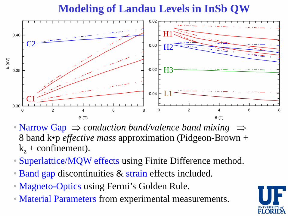
Modeling of Landau Levels in InSb QW
B (T)
0 2 4 6 8
E (e
V)
-0.04
-0.02
0.00
0.02
H1
H2
H3
L1
• Narrow Gap ⇒ conduction band/valence band mixing ⇒8 band k•p effective mass approximation (Pidgeon-Brown + kz + confinement).
• Superlattice/MQW effects using Finite Difference method.• Band gap discontinuities & strain effects included.• Magneto-Optics using Fermi’s Golden Rule.• Material Parameters from experimental measurements.
B (T)
0 2 4 6 8
E (e
V)
0.30
0.35
0.40
C1
C2
t212b (p=3.5x1011cm-2)
Frequency (cm-1)
20 40 60 80 100 120
T(B
)/T(0
)
1.0
1.5
2.0
2.5
3.0
2.0T
7.0T
6.0T
5.0T
4.0T
3.0T
6.5T
5.5T
4.5T
3.5T
2.5T
t212b (p=3.5x1011cm-2)
Frequency (cm-1)
100 150 200 250
T(B
)/T(0
)
1.0
1.2
1.4
1.6
1.8
2.0
InSb
pho
nons
GaA
s ph
onon
s
7.0T
8.0T
9.0T
10.0T
11.0T
12.0T
13.0T
14.0T
9.5T
10.5T
11.5T
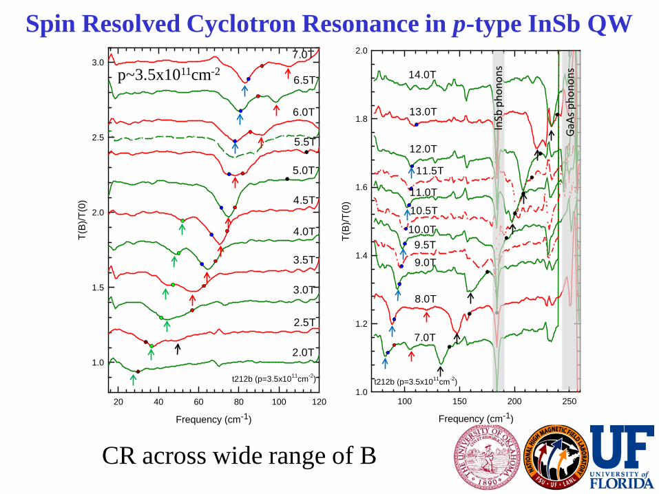
Spin Resolved Cyclotron Resonance in p-type InSb QW
p~3.5x1011cm-2
CR across wide range of B
t212p=3.5x1011cm-2
B (T)
0 2 4 6 8 10 12 14
Ene
rgy
(eV
)
0.00
0.01
0.02
0.03 H10d-H11d H10u-H11u H11d-H12d H11u-H12u
t212p=3.5x1011cm-2
B (T)
0 2 4 6 8 10 12 14
Ene
rgy
(eV
)
0.00
0.01
0.02
0.03 H10d-H11d H10u-H11u H11d-H12d H11u-H12u
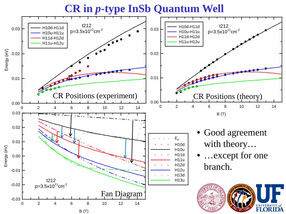
CR Positions (experiment)
• Good agreement with theory…
• …except for one branch.
CR in p-type InSb Quantum Well
CR Positions (theory)
t212p=3.5x1011cm-2
B (T)
0 2 4 6 8 10 12 14
Ene
rgy
(eV
)
-0.03
-0.02
-0.01
0.00
0.01
0.02
0.03
EF
H10d H10u H11d H11u H12d H12u H13d H13u
Fan Diagram
B (T)
0 2 4 6 8 10 12 14 16 18
ν (c
m-1
)
0
50
100
150
200
250
300
0.05mo
0.10mo
t196bt196b
t196bp~2x1011cm-2
B (T)
0 2 4 6 8 10 12 14 16 18
ν (c
m-1
)
0
50
100
150
200
250
300
0.05mo
0.10mo
t194ct194c
t194cp~3x1011cm-2
B (T)
0 2 4 6 8 10 12 14 16 18
ν (c
m-1
)
0
50
100
150
200
250
300
0.05mo
0.10mo
t198bt198bt198b
t198bp~5x1011cm-2
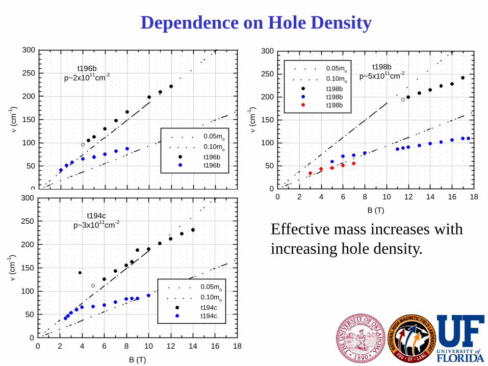
Dependence on Hole Density
Effective mass increases with increasing hole density.

SummaryMolecular Beam Epitaxy of InSb-based heterostructures• Mobility partially limited by micro-twins and dislocations• Defect densities depends on buffer layer composition• Room temperature mobility as high as 41,000 cm2/Vs
Electron transport through InSb mesoscopic structures• Ballistic transport observed at T~200K in 0.5µm devices • Quantized conductance observed in point contacts• Magnetic focusing features observed
2D Hole systems in InSb quantum wells• Mobility lower than for 2D electron systems• Cyclotron resonance shows m*≥0.04me• Good prototype system for p-type III-V quantum wells