
InP High Electron Mobility Transistor Design for Cryogenic ...
52
THESIS FOR THE DEGREE OF LICENTIATE OF ENGINEERING InP High Electron Mobility Transistor Design for Cryogenic Low Noise Amplifiers EUNJUNG CHA Microwave Electronics Laboratory Microtechnology and Nanoscience - MC2 CHALMERS UNIVERSITY OF TECHNOLOGY Gothenburg, Sweden 2018 brought to you by CORE View metadata, citation and similar papers at core.ac.uk provided by Chalmers Research
Transcript of InP High Electron Mobility Transistor Design for Cryogenic ...

THESIS FOR THE DEGREE OF LICENTIATE OF ENGINEERING
InP High Electron Mobility Transistor Design for
Cryogenic Low Noise Amplifiers
EUNJUNG CHA
Microwave Electronics LaboratoryMicrotechnology and Nanoscience - MC2
CHALMERS UNIVERSITY OF TECHNOLOGY
Gothenburg, Sweden 2018
brought to you by COREView metadata, citation and similar papers at core.ac.uk
provided by Chalmers Research

InP High Electron Mobility Transistor Design for Cryogenic Low Noise Ampli-fiersEUNJUNG CHA
c� EUNJUNG CHA, March 2018
Chalmers University of TechnologyMicrotechnology and Nanoscience - MC2Microwave Electronics LaboratorySE-412 96 Gothenburg, SwedenPhone: +46(0)31 772 1000
ISSN 1652-0769Technical Report MC2-387
Cover:Cross sectional STEM image of the InP HEMT
Printed by Chalmers ReproserviceGothenburg, Sweden March 2018

Abstract
The InGaAs/InAlAs/InP high electron mobility transistor (InP HEMT) isthe superior technology for the most demanding low-noise and high-speedmicrowave and millimeter-wave applications, in particular in radio astronomyand deep-space communication. InP HEMT has enabled cryogenic low noiseamplifier (LNA) designs with noise temperatures about ten times the quantumnoise limit from sub GHz up to 120 GHz. In this thesis, design techniquesof 100 nm gate length InP HEMTs for state-of-the-art cryogenic LNAs arereported. Detailed DC, RF and noise analysis for the InP HEMTs at 300 Kand 5 K are presented. The thesis is divided into two parts.
The first part of the work reports on the optimization of 100 nm gate lengthInP HEMT technology for cryogenic LNA applications at microwave frequencies.By scaling the gate length and barrier thickness combined with reduction ofsource and gate resistances, advances in cryogenic noise performance for wide-band monolithic microwave integrated circuit (MMIC) LNA were demonstratedin the frequency range 0.3�28 GHz. At 4K, the minimum noise temperaturewas 2.2K and 4.8K for a 0.3�14 GHz and 16�28 GHz LNA, respectively. Thecryogenic MMIC LNAs demonstrated state-of-the-art noise performance.
In the second part, cryogenic stability of two-finger InP HEMTs is inves-tigated. The InP HEMTs exhibited anomalous behavior in terms of jumpsin drain current, sharp peaks in transconductance, and decreased gain undercryogenic operation. Three di↵erent design techniques for two-finger HEMTswere tested to mitigate the anomalous instabilities associated with cryogenicoperation. By either adding a source air-bridge, connecting the back end ofgates or increasing the gate resistance, stable device operation was demon-strated for each case. Successful stabilization was confirmed both on deviceand circuit level by cryogenic measurements. A three-stage 24–40 GHz anda four-stage 28–52 GHz MMIC LNA based on the source air-bridge designtechnique for the two-finger InP HEMTs were demonstrated at 5.5K. The min-imum noise temperature was 7K and 6.7K in the 24�40 GHz and 28�52 GHzLNA, respectively. Both designs demonstrated the lowest noise temperaturereported so far for cryogenic MMIC LNAs for these frequency bands.
Keywords: cryogenic, InP HEMT, LNA, MMIC, noise temperature, stability.
i

ii

List of publications
Appended papers
This thesis consists of an extended summary and the following appended
papers:
[A] Eunjung Cha, Giuseppe Moschetti, Niklas Wadefalk, Per-Ake Nilsson,
Stella Bevilacqua, Arsalan Pourkabirian, Piotr Starski, and Jan Grahn,“Two-
Finger InP HEMT Design for Stable Cryogenic Operation of Ultra-Low-Noise
Ka- and Q-Band LNAs”, IEEE Transactions on Microwave Theory and Tech-
niques, vol. 65, no. 12, pp. 5171-5180, Dec 2017. DOI: 10.1109/TMTT.2017.2765318
[B] Eunjung Cha, Niklas Wadefalk, Per-Ake Nilsson, Joel Schleeh, Giuseppe
Moschetti, Arsalan Pourkabirian, Silvia Tuzi, and Jan Grahn,“0.3�14- and
16�28-GHz Wide-Bandwidth Cryogenic MMIC Low-Noise Amplifiers”, sub-
mitted, 2017.
[C] Eunjung Cha, Arsalan Pourkabirian, Joel Schleeh, Niklas Wadefalk,
Giuseppe Moschetti, Piotr Starski, Goran Alestig, John Halonen, Bengt Nilsson,
Per-Ake Nilsson, and Jan Grahn,“Cryogenic low-noise InP HEMTs: A source-
drain distance study”, in International Conference on Indium Phosphide and
Related Materials (IPRM), Toyama, Japan, 2016.
Other papers and publications
The following papers and publications are not appended to the thesis, either
due to contents overlapping with appended papers, or due to contents not
related to the thesis.
[a] Eunjung Cha, Giuseppe Moschetti, Niklas Wadefalk, Per-Ake Nilsson,
iii

Stella Bevilacqua, Arsalan Pourkabirian, Piotr Starski, and Jan Grahn, “Two-
Finger InP HEMT Design for Stable Cryogenic Operation of Ultra-Low-Noise
Ka-Band LNAs”, in 2017 IEEE MTT-S International Microwave Symposium
(IMS), Honolulu, Hawaii, 2017.
[b] Joel Schleeh, Giuseppe Moschetti, Niklas Wadefalk, Eunjung Cha, Arsalan
Pourkabirian, Goran Alestig, John Halonen, Bengt Nilsson, Per-Ake Nilsson,
and Jan Grahn, “Cryogenic LNAs for SKA band 2 to 5”, in 2017 IEEE MTT-S
International Microwave Symposium (IMS), Honolulu, Hawaii, 2017.
[c] Yulung Tang, Niklas Wadefalk, Jacob W Kooi, Joel Schleeh, Giuseppe
Moschetti, Per-Ake Nilsson, Arsalan Pourkabirian, Eunjung Cha, Silvia Tuzi,
and Jan Grahn, “Cryogenic W-band LNA for ALMA band 2+3 with average
noise temperature of 24 K” in 2017 IEEE MTT-S International Microwave
Symposium (IMS), Honolulu, Hawaii, 2017.
iv

v

vi

Contents
Abstract i
List of publications iii
1 Introduction 1
2 InP HEMT scaling for cryogenic LNAs 32.1 Vertical and lateral scaling . . . . . . . . . . . . . . . . . . . . . 32.2 Access resistance reduction . . . . . . . . . . . . . . . . . . . . 8
2.2.1 Source resistance . . . . . . . . . . . . . . . . . . . . . . 82.2.2 Gate resistance . . . . . . . . . . . . . . . . . . . . . . . 13
2.3 0.3�14 GHz and 16�28 GHz MMIC LNA demonstration . . . 14
3 InP HEMT design for stable cryogenic operation 193.1 Stability characterization . . . . . . . . . . . . . . . . . . . . . 193.2 Design technique . . . . . . . . . . . . . . . . . . . . . . . . . . 23
3.2.1 Source air-bridge . . . . . . . . . . . . . . . . . . . . . . 243.2.2 Two gate fingers back end connection . . . . . . . . . . 263.2.3 Gate resistance modification . . . . . . . . . . . . . . . . 26
3.3 24�40 GHz and 28�52 GHz MMIC LNA demonstration . . . . 27
4 Conclusions and future work 314.1 Conclusions . . . . . . . . . . . . . . . . . . . . . . . . . . . . . 314.2 Future work . . . . . . . . . . . . . . . . . . . . . . . . . . . . . 31
Bibliography 33
Acknowledgements 41
Appended Papers 43
vii

viii

Chapter 1
Introduction
Since the invention of the high electron mobility transistor by T. Mimurain 1979,1 HEMTs have been the superior technology in the most demandinglow-noise and high-speed microwave and millimeter-wave applications, inparticular for radio astronomy and deep-space communication. In the HEMTheterostructure, the electrons are confined in the channel forming the two-dimensional electron gas where the impurity scattering with ionized donors issuppressed. As a results, an electron mobility becomes more than ten timeshigher than in silicon at a comparable sheet charge density meaning extremelyhigh-frequency and low-noise properties for the HEMT. The HEMT technologyhas shown marked improvement with cut-o↵ frequency (fT ) in excess of600GHz and maximum oscillation frequency (fmax) exceeding 1THz.2–7
One of the great challenges in radio astronomy and deep-space communica-tion is to detect extremely weak signals.8 For a given antenna, the microwavefrontend controls the receiving system sensitivity (S) where S is the quotientS = G/Tsys between the antenna gain (G) and the noise temperature (Tsys)of the entire receiving chain. Thus improved receiving performance can beachieved by either increasing G or reducing Tsys, or both. It is more e�cientand cost e↵ective to decrease Tsys, in particular by improving the LNA in thefirst stages of the receiver system, than to improve G which is related to theantenna size and geometry. The noise temperature of the LNA is crucial forTsys. As a result, such an LNA is normally operated at cryogenic temperature,typically 5�15 K. The transistor technology used for the cryogenic LNA designis here decisive for the noise temperature.
The InGaAs/InAlAs/InP HEMT enables the design of cryogenic LNAswith noise temperatures about ten times the quantum noise limit from subGHz up to 120 GHz.9–16 Further noise improvement is desirable since a smallreduction in noise temperature means higher data reception capability. Inaddition, pushing the ultra-low noise HEMT technology is also important forresearch related to quantum physics, such as readout of qubits in quantumcomputing applications.
The goal of this thesis is to present design techniques for 100 nm gate lengthInP HEMTs for new state-of-the-art cryogenic LNA up to 50GHz. Scaling ofthe gate length and the barrier thickness combined with reduction of sourceand gate resistances of the InP HEMT have been carried out with respect tonoise performance in the cryogenic LNA. Furthermore, design techniques of thetwo-finger HEMTs for stable cryogenic operation are reported. The cryogenicinstability observed in two-finger InP HEMTs is discussed and stabilization
1

CHAPTER 1. INTRODUCTION
solutions are presented. The stabilized InP HEMTs were implemented in24�40GHz and 28�52GHz cryogenic MMIC LNAs, resulting in state-of-the-art noise performance.
In Chapter 2, the InP HEMT scaling optimized for cryogenic LNA applica-tion is discussed. Chapter 3 presents the two-finger HEMT design techniquesfor stable cryogenic operation. Finally, Chapter 4 summarizes the results ofthis thesis and provides a future outlook.
2

Chapter 2
InP HEMT scaling for cryogenicLNAs
In order to predict the minimum noise temperature (Tmin) of the HEMT, anempirical expression suggested by M. Pospieszalski17 is widely used:
Tmin ⇡ 2f
fT
q(Rs +Rg +Ri)TgGdsTd (2.1)
where Rs, Rg, and Ri are the source, gate, and intrinsic channel resistances,respectively. Gds is the output conductance, Tg is the equivalent temperatureof Ri, and Td is the equivalent temperature of Gds. One way of improving thenoise performance of HEMT is to maximize the intrinsic fT and to minimizethe parasitic source and gate resistances. However, an aggressive scaling ofthe Schottky barrier thickness of the HEMT for highest possible fT will endup increasing the gate leakage current and gate-to-channel capacitance whichin turn deteriorate the low-noise performance.10,17–19 A thin barrier willalso increase the channel depletion and thus the intrinsic resistance due tosurface states being closer to the channel.20 Therefore, a well-balanced verticaland lateral scaling of the HEMTs is required in order to improve the noiseperformance of the cryogenic LNA.
This chapter addresses an optimized InP HEMT design for cryogenic LNAapplications for microwave frequencies. The optimization includes the scalingof the barrier layer and the gate length as well as parasitic resistance reduction.The DC characterization, S-parameters, and noise analysis of the HEMTs arepresented at 300 K and 5 K. In addition, this chapter reports on the noiseperformance of two broadband cryogenic MMIC LNAs operating at 0.3–14GHzand 16–28 GHz which implemented the optimized 100 nm gate length InPHEMTs.
2.1 Vertical and lateral scaling
The epitaxial layer structure used in this work (see Fig. 2.1) was grown on400 InP wafers by molecular beam epitaxy. The epitaxial layer was purchasedfrom IntelliEpi. Hall measurements at 300 K without the cap layer exhibitedan electron mobility and sheet carrier concentration of 10,850 cm2/Vs and3.3⇥1012 cm�2, respectively. The detailed description of the InP HEMT
3

CHAPTER 2. INP HEMT SCALING FOR CRYOGENIC LNAS
Figure 2.1: The epitaxial layer structure used in this work.
Figure 2.2: I-V characteristics of a 2 ⇥ 100 µm gate width and 100 nm gatelength InP HEMT. Vgs measured from �0.5 V to 0.4 V in steps of 0.04 V(left). Extrinsic transconductance versus drain current density. Vds measuredfrom 0.1 V to 1 V in steps of 0.1 V (right).
fabrication process can be found in Paper [A]. The barrier thickness was 3 nmless than that (11 nm) of our previously reported HEMTs.10,21 In addition, thegate length was scaled from 130 nm to 100 nm.10,21 DC and RF measurementsof the scaled HEMTs were performed in a LakeShore model CRX-4K cryogenicprobe station at 300 and 5 K. Fig. 2.2 shows the output characteristics ofa 2⇥100 µm HEMT. The maximum drain current density (Id) at the drain-source voltage (Vds) of 1 V are 500 mA/mm at 300 K and 650 mA/mm at 5K.A kink in the drain current for about Vds = 0.3 V is observed at 5 K. This iswell known electric instability for cryogenic InP HEMTs related to trappingprocesses occurring at the interfaces and surface of the heterostructure.22–25
Normally the kink phenomenon is not a problem for a cryogenic LNA sincethe InP HEMT is biased close to the pinch-o↵ region. However, if the trappingcauses memory e↵ects in the HEMT, this may jeopardize reliable cryogenicLNA operation.
The DC transconductance (gm) as a function of Id is shown in Fig. 2.2.
4
CHAPTER 2. INP HEMT SCALING FOR CRYOGENIC LNAS
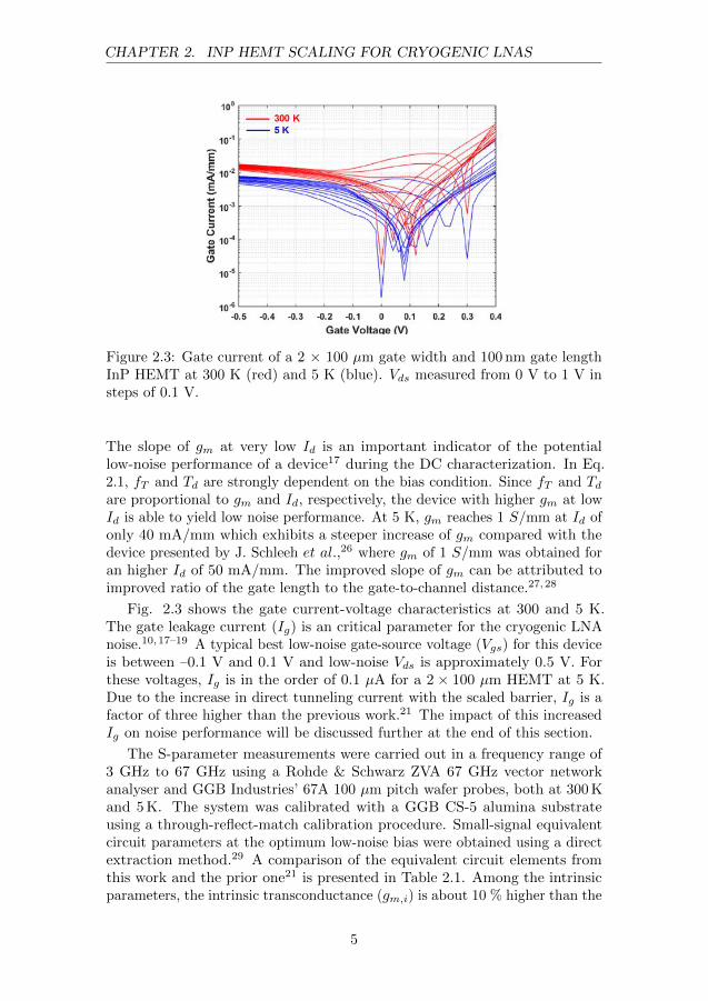
Figure 2.3: Gate current of a 2 ⇥ 100 µm gate width and 100 nm gate lengthInP HEMT at 300 K (red) and 5 K (blue). Vds measured from 0 V to 1 V insteps of 0.1 V.
The slope of gm at very low Id is an important indicator of the potentiallow-noise performance of a device17 during the DC characterization. In Eq.2.1, fT and Td are strongly dependent on the bias condition. Since fT and Td
are proportional to gm and Id, respectively, the device with higher gm at lowId is able to yield low noise performance. At 5 K, gm reaches 1 S/mm at Id ofonly 40 mA/mm which exhibits a steeper increase of gm compared with thedevice presented by J. Schleeh et al.,26 where gm of 1 S/mm was obtained foran higher Id of 50 mA/mm. The improved slope of gm can be attributed toimproved ratio of the gate length to the gate-to-channel distance.27,28
Fig. 2.3 shows the gate current-voltage characteristics at 300 and 5 K.The gate leakage current (Ig) is an critical parameter for the cryogenic LNAnoise.10,17–19 A typical best low-noise gate-source voltage (Vgs) for this deviceis between –0.1 V and 0.1 V and low-noise Vds is approximately 0.5 V. Forthese voltages, Ig is in the order of 0.1 µA for a 2 ⇥ 100 µm HEMT at 5 K.Due to the increase in direct tunneling current with the scaled barrier, Ig is afactor of three higher than the previous work.21 The impact of this increasedIg on noise performance will be discussed further at the end of this section.
The S-parameter measurements were carried out in a frequency range of3 GHz to 67 GHz using a Rohde & Schwarz ZVA 67 GHz vector networkanalyser and GGB Industries’ 67A 100 µm pitch wafer probes, both at 300Kand 5K. The system was calibrated with a GGB CS-5 alumina substrateusing a through-reflect-match calibration procedure. Small-signal equivalentcircuit parameters at the optimum low-noise bias were obtained using a directextraction method.29 A comparison of the equivalent circuit elements fromthis work and the prior one21 is presented in Table 2.1. Among the intrinsicparameters, the intrinsic transconductance (gm,i) is about 10 % higher than the
5

CHAPTER 2. INP HEMT SCALING FOR CRYOGENIC LNAS
Table 2.1: Extracted parameters for the small-signal equivalent circuit of2⇥ 100 µm InP HEMT at the optimum low-noise bias as 300 K and 5 K. Unitsare V, mA, mS, ⌦, fF, pH, and K.
This work Ref. 21300 K 5 K 300 K 10 K
Bias Vds 0.6 0.4 1 0.6Id 16.7 5 15 5Vgs -0.02 -0.05 -0.19 -0.16
Intrinsic Cgs 133 139 137 148Cgd 41 43 31 36Cds 84 59 50 51gm,i 256 244 207 223Ri 3.2 0.3 4.1 2.2Rj 34 21 36 27Gds 16 17 11 14
Extrinsic Cpg, Cpd 20 20 8 8Lg 6 5 8 10Ls 0 0 0 0Ld 5 5 8 10Rg 1.9 0.6 4 2Rd 2.0 0.8 3 2Rs 1.8 0.8 2 1
Figure 2.4: Intrinsic current gain |H21|2 of a 2 ⇥ 100 µm gate width and100 nm gate length InP HEMT at the optimum low-noise bias at 300 K (red)and 5 K (blue).
previously techonology21 at 5 K. It is also noticed that the extrinsic parameters
6
CHAPTER 2. INP HEMT SCALING FOR CRYOGENIC LNAS
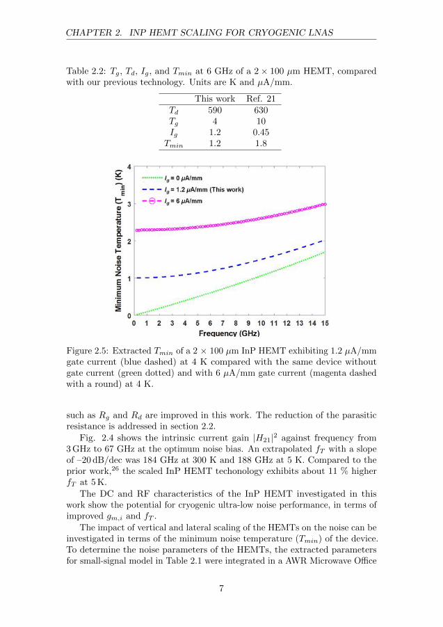
Table 2.2: Tg, Td, Ig, and Tmin at 6 GHz of a 2⇥ 100 µm HEMT, comparedwith our previous technology. Units are K and µA/mm.
This work Ref. 21Td 590 630Tg 4 10Ig 1.2 0.45
Tmin 1.2 1.8
Figure 2.5: Extracted Tmin of a 2 ⇥ 100 µm InP HEMT exhibiting 1.2 µA/mmgate current (blue dashed) at 4 K compared with the same device withoutgate current (green dotted) and with 6 µA/mm gate current (magenta dashedwith a round) at 4 K.
such as Rg and Rd are improved in this work. The reduction of the parasiticresistance is addressed in section 2.2.
Fig. 2.4 shows the intrinsic current gain |H21|2 against frequency from3GHz to 67 GHz at the optimum noise bias. An extrapolated fT with a slopeof –20 dB/dec was 184 GHz at 300 K and 188 GHz at 5 K. Compared to theprior work,26 the scaled InP HEMT techonology exhibits about 11 % higherfT at 5K.
The DC and RF characteristics of the InP HEMT investigated in thiswork show the potential for cryogenic ultra-low noise performance, in terms ofimproved gm,i and fT .
The impact of vertical and lateral scaling of the HEMTs on the noise can beinvestigated in terms of the minimum noise temperature (Tmin) of the device.To determine the noise parameters of the HEMTs, the extracted parametersfor small-signal model in Table 2.1 were integrated in a AWR Microwave O�ce
7

CHAPTER 2. INP HEMT SCALING FOR CRYOGENIC LNAS
model of the LNA. Td was extracted by fitting the simulated noise to themeasurement of the LNA.30 Ig was modeled with a shot noise current sourceusing a DC gate current of 1.2µA/mm measured at the optimum noise biasat cryogenic temperature.19,31
Table 2.2 shows Td, Tg, Ig, and Tmin obtained from the scaled InP HEMTtechnology compared to the prior work.21 The physical temperature was set tobe 4K corresponding to the LNA test ambient (see section 2.3). It is observedthat a 0.6K lower Tmin at 6 GHz was achieved despite the fact that the 3 nmthinner barrier thickness increased Ig by 60 %. This can be explained in termsof the improvement in gm,i and fT , whereas Ig does not still dominate thenoise.17,18
The simulated Tmin with three di↵erent Ig is plotted as a function offrequency in Fig. 2.5. The impact of Ig on Tmin is much stronger at lowfrequencies.17–19 Consequently, a too high Ig will significantly a↵ect the noiseperformance at a few GHz. The InP HEMT with Ig = 1.2 µA/mm has roughly100 % higher Tmin (1.2 K) at 6 GHz than the device with Ig = 0µA/mm. Inthe case of five-fold higher Ig = 6 µA/mm, Tmin of the HEMT increases to2.4K (+300%) which even exceeds the minimum noise temperature (Te,min)of the 0.3�14 GHz LNA in this work (see Fig. 2.14). As reported by M.Pospieszalski17 and J. Shell,18 when Ig is of the order of 0.1 µA, the devicecould still yield low-noise performance. In this work, the 2 ⇥ 100 µm InPHEMT exhibited Ig of 0.24µA at the optimum noise bias which is small enoughnot to dominate the noise performance. However, it is expected that furtherincrease in Ig may significantly deteriorate the noise performance as seen inFig. 2.5.
2.2 Access resistance reduction
Minimizing the parasitic resistances is another key parameter for reducing thenoise contribution of the device17 as shown in Eq. 2.1. In this work, the sourceaccess resistance as well as the gate resistance have been optimized and theirimpact onto the device as well as noise performance have been investigated.
2.2.1 Source resistance
To improve the ultimate performance of HEMTs, the reduction of Rs plays acentral role.32–34 In order to benefit from high gm,i of the HEMT, Rs shouldbe kept small compared to the inverse of gm,i which in turn yields the noisereduction. Rs is a↵ected by surface states on top of the barrier and by trapsbetween bu↵er and bottom of the channel.20,22,35,36 Therefore, scaled barrierin this work will possibly cause increased Rs. In order to reduce Rs, the contactresistance between the ohmic metal and the epitaxial layers (cap, barrier, andchannel) should be minimized. This was necessary since the barrier layer wasmodified in this work. In addition, by decreasing the distance between thegate and the source metal contacts, Rs can be further reduced.
8

CHAPTER 2. INP HEMT SCALING FOR CRYOGENIC LNAS
Figure 2.6: Contact resistance measured at 300 K from recessed TLM structures(left) and specific contact resistivity measured from Kelvin structures (right)as a function of annealing temperature.
Ohmic contact resistance
Various combinations as metal stacks in ohmic contacts have been reported.32,37–41
In addition to the used metals, the annealing conditions, such as temperature,time, and ambient, have large impact on the contact resistance. In this work,a Ni/Ge/Au ohmic metal stack, which was subject to rapid thermal annealin an N2 ambient, was used. During the annealing process, the Ni enhancesthe reaction between the contact metal and the semiconductor, and the Alin the InAlAs barrier layer out-di↵uses to the surface of the contact metal.37
Then a small fraction of Ge atoms substitutes at these Al sites, resulting inthe formation of a Ge-doped n
+�InAlAs layer which increases the carriertunneling probability, thus reducing the contact resistance.37 The annealingtemperature and time were swept as illustrated in Fig. 2.6 in order to find theoptimum condition. The contact resistance was measured from the recessedtransfer length method (TLM). In addition, the specific contact resistivity wasmeasured using a Kelvin structure.42 Fig. 2.6 shows that an optimized ohmiccontact was obtained when annealing at 315 �C for 1 min 30 s which resulted ina contact resistance of 0.05 ⌦·mm and a specific contact resistivity of 4⇥10�7⌦·cm2. The contact resistance measured using the non-recessed TLM (not shownhere) resulted in a contact resistance of 0.03 ⌦·mm which is comparable toprior work.10 An extremely low contact resistance of 0.007⌦ ·mm for an InPHEMT was reported by K. Shinohara et al.43 who employed a multilayercap structure and a non-alloyed ohmic contact. In addition, the non-alloyedcontact resistance demonstrates a long-time thermal stability44 and a nearlytemperature independent contact resistance.41 Hence there is a potential toreduce the present ohmic contact resistance by a factor of 3 to 4 using a moreadvanced cap layer in combination with non-alloyed contact formation.
9
CHAPTER 2. INP HEMT SCALING FOR CRYOGENIC LNAS
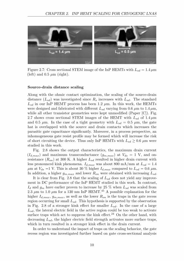
Figure 2.7: Cross sectional STEM image of the InP HEMTs with Lsd = 1.4µm(left) and 0.5 µm (right).
Source-drain distance scaling
Along with the ohmic contact optimization, the scaling of the source-draindistance (Lsd) was investigated since Rs increases with Lsd. The standardLsd in our InP HEMT process has been 1.2 µm. In this work, the HEMTswere designed and fabricated with di↵erent Lsd varying from 0.6 µm to 1.4µm,while all other transistor geometries were kept unmodified (Paper [C]). Fig.2.7 shows cross sectional STEM images of the HEMT with Lsd of 1.4µmand 0.5 µm. In the case of a tight geometry with Lsd = 0.5 µm, the gatehat is overlapped with the source and drain contacts which increases theparasitic gate capacitance significantly. Moreover, in a process perspective, aninhomogeneous gate resist profile may be formed which will increase the riskof short circuiting the device. Thus only InP HEMTs with Lsd � 0.6 µm werestudied in this work.
Fig. 2.8 shows the output characteristics, the maximum drain current(Id,max) and maximum transconductance (gm,max) at Vds = 1 V, and on-resistance (Ron) at 300 K. A higher Lsd resulted in higher drain current withless pronounced kink phenomena. Id,max was about 800 mA/mm at Lsd = 1.4µm at Vds =1 V. This is about 30 % higher Id,max compared to Lsd = 0.6 µm.In addition, a higher gm,max and lower Ron were obtained with increasing Lsd.
It is clear from Fig. 2.8 that the scaling of Lsd does not yield any improve-ment in DC performance of the InP HEMT studied in this work. In contrast,Id and gm have earlier proven to increase by 25 % when Lsd was scaled from2.3 µm to 1.0 µm for a 130 nm InP HEMT.45 A possible explanation for thehigher Id,max, gm,max, as well as the lower Ron is the traps in the gate recessregion occurring for small Lsd. This hypothesis is supported by the observationin Fig. 2.8 of a stronger kink e↵ect for smaller Lsd. In the case of a largeLsd, the lateral electric field in the active region could be too weak to activatesurface traps which act to suppress the kink e↵ect.24 On the other hand, withdecreasing Lsd, the higher electric field strength activates more surface traps,which in turn resulted in a stronger kink e↵ect in the drain current.
In order to understand the impact of traps on the scaling behavior, the gaterecess region was investigated further based on gate cross-sectional analysis
10

CHAPTER 2. INP HEMT SCALING FOR CRYOGENIC LNAS
Figure 2.8: The output characteristics of 2 ⇥ 100 µm InP HEMTs at 300Kwith Lsd ranging from 0.6 µm to 1.4 µm. Vgs measured from �0.3 V to 0.7Vin steps of 0.25 V (upper left). The maximum drain current (upper right),maximum transconductance at Vds = 1 V (lower left), and on-resistance (lowerright) as a function of Lsd.
by a scanning transmission electron microscope (STEM). While a wide recessimproves breakdown voltage and reduces the feedback capacitance and the gateleakage current, the parasitic source and drain access resistance are increasedwhich reduces the transconductance.46–48 A typical recess region is shownin Fig. 2.9 (left). During the gate recess etching process, the cap layer wasselectively wet etched using succinic acid mixed with H2O2 in 4:5 ratio for40 s and rinsed in water,49 which gave a 100 nm wide side-recess spacing. It isnotable that the InAlAs barrier layer was also etched during recess etching dueto the limited selectivity of gate recess wet etching. In addition, the recessedbarrier in Fig. 2.9 (left) is not completely flat having dimples at the edges ofthe gate recessed region. The kink e↵ect highly depends on the recess regionas the kink arises from the change in the channel electron density in the recessregion.22,36,51 Therefore, the observation of a non-uniform recess depth asshown in Fig. 2.9 (left) may be one explanation of the strong kink e↵ect andthe contradictory scaling behavior of Lsd in Fig. 2.8.
11

CHAPTER 2. INP HEMT SCALING FOR CRYOGENIC LNAS
Figure 2.9: STEM images of the gate region without agitation in water (left)and with agitation in water (right) after the gate recess etching.
Figure 2.10: The output characteristics of 2⇥ 100 µm InP HEMTs at 300Kwith Lsd ranging from 0.6 µm to 2.2 µm. Vgs measured from �0.5 V to 0.4Vin steps of 0.1 V (upper left). The maximum drain current (upper right),maximum transconductance at Vds = 1 V (lower left), and on-resistance (lowerright) as a function of Lsd.
12

CHAPTER 2. INP HEMT SCALING FOR CRYOGENIC LNAS
Figure 2.11: Cross sectional STEM image of the InP HEMTs with Rg =320⌦/mm10,21,50 (left) and Rg = 230 ⌦/mm (right) measured at 300 K.
The dimples at the edges of the recess could be caused by the fact that ittakes longer to remove the acid at the far edges since the space where the waterhas to flow is very tight. Therefore, proper agitation in water, alternativelymegasonic cleaning, can help to suppress the non-uniform gate recess etching.In this work, a strong agitation in water after wet etching was tested. Inaddition, the recess etching time was shorten from 40 s to 30 s in order toexplore the impact of the side-recess spacing on Lsd scaling. As shown in Fig.2.9 (right), the recess was 50 nm wide and the dimples at the edges of therecess region disappeared leaving a flat surface in the gate recess. Devices withdi↵erent Lsd ranging from 0.6µm to 2.2µm were designed, fabricated, andcharacterized as can be seen in Fig. 2.10. The kink e↵ect is clearly suppressedin the I�V characteristics which means that less traps seem to be present inthese narrow recess regions without dimples. In addition, an increase in Id,max
and gm,max and decrease in Ron are observed for small Lsd. In contrast to Fig.2.8, the results in Fig. 2.10 are consistent with the scaling of the Lsd for theHEMTs published by M. Malmkvist.45 It is concluded that proper scaling ofthe InP HEMT can only be done using a uniform gate recess etching wherethe surface traps are well suppressed.
2.2.2 Gate resistance
With the aim to further minimize the parasitic resistance for the low noiseHEMTs, Rg was reduced from 320 ⌦/mm to 230 ⌦/mm at 300 K, and from130⌦/mm to 50 ⌦/mm at 5 K.10,21 Rg was measured in a gate through-linetest structure. Fig. 2.11 compares two gate structures with Rg = 320⌦/mm(left) and Rg = 230 ⌦/mm (right) measured at 300 K. The T-gate fabricationprocess was optimized by adjusting the electron beam current dose and using aproper resist for a mechanically stable and low resistance gate structure. As aresult, Fig. 2.11 (right) shows an improved gate foot and hat connection whichresulted in larger mechanical stability as well as a reduced Rg. In addition,
13

CHAPTER 2. INP HEMT SCALING FOR CRYOGENIC LNAS
Figure 2.12: Impact of the gate resistance on Tmin of a 2⇥ 100 µm InP HEMTexhibiting Rg = 50 ⌦/mm (blue dashed) compared with the same device withRg = 130⌦/mm (magenta solid) at 4 K.
about 20 % increase in the gate hat size in Fig. 2.11 (right) also contributedto a reduction in Rg obtained in this work.
In Fig. 2.12, the importance of gate resistance is illustrated by showingtwo modeled 2⇥ 100 µm InP HEMTs either with Rg = 50 ⌦/mm or with Rg
= 130 ⌦/mm. It should be emphasized that the improvement of the noisetemperature due to the reduction in Rg by 60 % at cryogenic temperature ismore pronounced at high frequencies above 10 GHz.
2.3 0.3�14 GHz and 16�28 GHz MMIC LNAdemonstration
The optimized low noise InP HEMT with 8 nm InAlAs barrier, 100 nm gatelength, Lsd = 1.4 µm, and Rg = 230 ⌦/mm (at 300 K) were implemented in0.3�14 GHz and 16�28 GHz MMIC LNAs. The MMICs presented in thiswork were fabricated before the optimization of gate recess processing. Thus,Lsd was designed to be 1.4 µm according to the results shown in Fig. 2.8.The 0.3�14 GHz MMIC LNA was of particular interest since the design wasidentical to the one using the prior InP HEMT technology.21 In this way, theimpact from the proposed InP HEMT design in this work on the cryogenicLNA performance became visible.
Fig. 2.13 shows photographs of the 0.3�14 GHz and 16�28GHz LNAs.Both chip sizes are 2 mm ⇥ 0.75 mm. The three-stage 0.3�14GHz GHz LNAuses 2 ⇥ 100 µm transistors and the 16�28 GHz LNA uses 2 ⇥ 50 µm HEMTs.MMIC design details can be found in Paper [B].
The best low noise bias for the 0.3�14 GHz LNA at 300 K was VD =
14

CHAPTER 2. INP HEMT SCALING FOR CRYOGENIC LNAS
Figure 2.13: MMIC photographs of the 0.3–14 GHz LNA (left) and the 16–28GHz LNA (right).
Figure 2.14: Measured (solid line) and simulated (dashed line) gain and noisetemperature of the 0.3�14 GHz LNA at 300 K. VD = 2 V, ID = 50 mA (left).Measured (solid line) and simulated (dashed line) gain and noise temperatureat 4 K. VD = 0.8 V, ID = 15 mA (right).
Figure 2.15: Measured (solid line) and simulated (dashed line) gain and noisetemperature of the 16�28 GHz LNA at 300 K. VD = 1.5 V, ID = 35 mA (left).Measured (solid line) and simulated (dashed line) gain and noise temperatureat 4 K. VD = 0.5 V, ID = 7 mA (right).
2 V and ID = 50 mA. Fig. 2.14 shows the measured and simulated noisetemperature and gain at 300 K. The LNA exhibits that the average noisetemperature (Te,avg) of 60.7 K with Te,min of 44.2 K at 8.2 GHz and 40.7 dB± 0.9 dB gain.
15

CHAPTER 2. INP HEMT SCALING FOR CRYOGENIC LNAS
When cooled down to 4 K, the optimum low noise bias for the LNA was VD
= 0.8 V and ID = 15 mA. As presented in Fig. 2.14, the amplifier achievedTe,avg of 3.5 K with Te,min of 2.2 K at 6 GHz and 41.6 dB ± 1.4 dB gain.
For the 16�28 GHz MMIC LNA at 300 K, Te,avg was 132.5 K with Te,min
of 95.5 K at 27.8 GHz and the gain was 35.5 dB ± 1.3 dB when biased at VD
= 1.5 V and ID = 35 mA as seen in Fig. 2.15.At the ambient temperature of 4 K, the LNA was biased at VD = 0.5 V
and ID = 7 mA and achieved a 32.3 dB ± 1.8 dB gain and Te,avg of 6.3 Kwith Te,min of 4.8 K at 20.8 GHz.
Table 2.3 displays a comparison of the two LNAs with other publishedcryogenic wide-bandwidth LNAs for similar frequency ranges.9,11,21,52–55 Thetwo LNAs presented in this work both exhibited state-of-the-art results interms of the lowest noise temperature and highest gain per stage with a widebandwidth at a relatively low power dissipation. Moreover, this was the firstdemonstration of cryogenic MMIC LNA covering the whole K-band (18 to27GHz).
The presented state-of-the-art results were achieved by the optimization ofInP HEMTs for cryogenic LNA applications. This can be explained by highergm,i and fT as well as parasitic resistance reduction for the InP HEMT. In thecase of the 0.3�14 GHz design, a too high Ig would have a large impact onthe LNA performance deteriorating the noise significantly.10,17–19 Despite thethree-fold higher Ig due to the scaled barrier, an improved noise temperaturewas achieved for the 0.3�14 GHz MMIC LNA. In the K-band, both the scalingof the HEMT and reduction in Rg were essential to yield a state-of-the-artcryogenic LNA noise performance.
16

CHAPTER 2. INP HEMT SCALING FOR CRYOGENIC LNAS
Table 2.3: Comparison of cryogenic wide-bandwidth LNAs.
Ref. Process Type Freq.(GHz)
Gain(dB)
Te,avg@Tamb(K)
Pdis
(mW)9 0.1 µm InP
HEMT3-stageMMIC
1-11 33.4±0.3 [email protected] 24
21 0.13 µm InPHEMT
3-stageMMIC
0.5-13 38.1 4.4@15 13
52 0.1 µm GaAsmHEMT
3-stageMMIC
4-12 31.5±1.8 5.3@15 8
53 0.1 µm InPHEMT
3-stageMMIC
4-12 37 3.5@12 9.2
54 0.1 µm InPHEMT
3-stageMMIC
4-12 26±1.2 8.1@15 12
Thiswork
0.1 µm InPHEMT
3-stageMMIC
0.3-14 41.6±1.4 3.5@4 12
11 80 nm InPHEMT
- 20-25 - 8@22 -
55 0.1 µm InPHEMT
4-stageHybrid
20-25 35 27@80 24
Thiswork
0.1 µm InPHEMT
3-stageMMIC
16-28 32.3±1.8 6.3@4 3.5
17

CHAPTER 2. INP HEMT SCALING FOR CRYOGENIC LNAS
18

Chapter 3
InP HEMT design for stablecryogenic operation
The InP HEMT technology has been developed to enable cryogenic LNAs tooperate at higher frequencies.56–60 For high frequencies, LNAs are built onMMICs in which an entire circuit is fabricated on a single chip. Therefore,reliable and reproducible cryogenic LNA operation can only be obtained whena transistor operates in a stable manner at cryogenic temperature.
Abnormal cryogenic HEMT operation has been reported in several stud-ies.18,60–65 G. Moschetti et al.64 reported that the four-finger metamorphicHEMT (mHEMT) exhibited a hysteretic change in the drain current, and asignificant reduction in gain at cryogenic temperature. The observed insta-bility was caused by a resonance induced by an U-shaped drain feeder whichconnects two drain contacts in the layout of the four-finger transistor. In orderto eliminate the resonances, an air-bridge was added across the drain feederwhich shifted the resonance frequency toward higher values beyond fmax ofthe mHEMT.
Another solution for stabilization of the cryogenic HEMT operation wasproposed by M. Varonen et al.60 The four-finger HEMTs were divided intotwo discrete two-finger HEMTs. In this way, oscillations at several hundreds ofGHz occurring within a four-finger device was avoided. The design techniqueproposed by M. Varonen et al.60 assumed that the two-finger devices werestable at cryogenic operation. However, instability of the two-finger deviceswere not yet discussed. This was in fact reported already in 1986.65 Thepresence of oscillations at several tens of GHz was noted, but the origin andsolution for instabilities were not found. Therefore, cryogenic instability intwo-finger InP HEMTs needs to be investigated more in detail. Such devicelayouts are frequently used in MMIC LNA designs.
In this chapter, the electric stability of two-finger InP HEMTs is investigatedat room and cryogenic temperature. Di↵erent stabilization solutions aresuggested and demonstrated both on device and circuit level by cryogenicmeasurements.
3.1 Stability characterization
The instability of various gate widths, ranging between 10 µm and 100 µm,and gate lengths, between 60 nm and 130 nm, of two-finger HEMTs at 300K
19

CHAPTER 3. INP HEMT DESIGN FOR STABLE CRYOGENICOPERATION
Figure 3.1: The I � V characteristics, transconductance at Vds = 0.8 V, andS21 at Vds = 0.8 V and Jd = 190 mA/mm of a 2 ⇥ 100 µm (left column),2⇥ 50µm (middle column) and 2⇥ 30 µm (right column) 100 nm HEMTs at300 K (red dashed) and 5 K (blue solid).
and 5K were investigated. DC measurements were carried out by sweepingthe drain voltage in steps of 25 mV for each gate voltage which was in steps of20mV. The S-parameter measurements were carried out in a frequency rangefrom 20 MHz to 60 GHz.
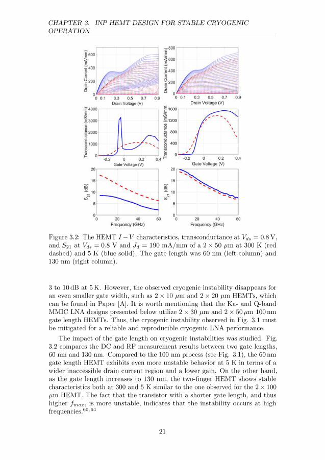
Fig. 3.1 presents the I�V characteristics, gm at Vds = 0.8 V and gain (S21)measured at Vds = 0.8 V and the drain current density (Jd) = 190mA/mmat 300 K and 5 K. The measured transistors were 2 ⇥ 100 µm, 2 ⇥ 50µm,and 2⇥ 30 µm 100 nm gate length HEMTs. The 2⇥ 100 µm HEMT shows acontinuous drain current and transconductance both at 300 K and 5K. Anincreased drain current and gain were also observed at 5 K compared to 300 Kwhich were consistent with the results seen in Fig. 2.2.18,63
As the gate width decreases, such as 2 ⇥ 50 µm and 2 ⇥ 30 µm HEMTsin Fig. 3.1, the drain current measured at 5 K suddenly increases with anabrupt step and exhibits a large output conductance not at all observed at300 K. This gives a drain current region which is not within reach using staticbias settings. Moreover, a discontinuous gm is observed for 2 ⇥ 50 µm and2⇥ 30µm HEMTs at 5 K. S21 is also significantly decreased by approximately
20
CHAPTER 3. INP HEMT DESIGN FOR STABLE CRYOGENICOPERATION
Figure 3.2: The HEMT I�V characteristics, transconductance at Vds = 0.8V,and S21 at Vds = 0.8 V and Jd = 190 mA/mm of a 2⇥ 50 µm at 300 K (reddashed) and 5 K (blue solid). The gate length was 60 nm (left column) and130 nm (right column).
3 to 10 dB at 5K. However, the observed cryogenic instability disappears foran even smaller gate width, such as 2⇥ 10 µm and 2⇥ 20 µm HEMTs, whichcan be found in Paper [A]. It is worth mentioning that the Ka- and Q-bandMMIC LNA designs presented below utilize 2⇥ 30 µm and 2⇥ 50µm 100 nmgate length HEMTs. Thus, the cryogenic instability observed in Fig. 3.1 mustbe mitigated for a reliable and reproducible cryogenic LNA performance.
The impact of the gate length on cryogenic instabilities was studied. Fig.3.2 compares the DC and RF measurement results between two gate lengths,60 nm and 130 nm. Compared to the 100 nm process (see Fig. 3.1), the 60 nmgate length HEMT exhibits even more unstable behavior at 5 K in terms of awider inaccessible drain current region and a lower gain. On the other hand,as the gate length increases to 130 nm, the two-finger HEMT shows stablecharacteristics both at 300 and 5 K similar to the one observed for the 2⇥ 100µm HEMT. The fact that the transistor with a shorter gate length, and thushigher fmax, is more unstable, indicates that the instability occurs at highfrequencies.60,64
21

CHAPTER 3. INP HEMT DESIGN FOR STABLE CRYOGENICOPERATION
Figure 3.3: The S-parameter measurements of the 2⇥ 50 µm device with a100 nm gate length at Vds = 0.3 V (green dashed), 0.6 V (blue solid), and0.9V (magenta dotted). Vgs = 0 V at an ambient temperature of 5 K.
It is concluded that anomalous cryogenic behavior for two-finger InP HEMTdepends on the device size as well as the gate length. The anomalies appearabove a certain device size, 2 ⇥ 20 µm, and disappear at larger gate width,2⇥ 100 µm. The instabilities become more pronounced with a shorter gatelength, 60 nm, whereas the investigated DC and RF characteristics for 130 nmInP HEMTs appear stable at 5 K.
The RF cryogenic setup in this study only allowed measurements up to67 GHz, so it was not possible to experimentally verify the high frequencyresonances reported in Ref. 64 to cause the observed device instabilities atcryogenic temperature. Instead, S-parameters were measured in a frequencyrange from 20 MHz to 67 GHz at 5 K. Fig. 3.3 presents the measured data upto 30 GHz where the abnormal features are observed. The bias point wherethe drain current suddenly increases is of particular interest. The 2⇥ 50 µm100 nm HEMT is measured at 5 K using Vds = 0.3, 0.6, and 0.9 V, and Vgs
= 0 V. As seen in Fig. 3.1, the drain current jumps at around Vds = 0.7 V.At a low drain drain bias of Vds = 0.3 V, the S-parameters do not show anyindication of instability. However, at Vds = 0.6 V, which is right before thedrain current jumps, the S-parameters start to deviate from the standardHEMT model. The S21 curve exhibits a spike at a few MHz and fluctuationsaround 5 GHz. In addition, in the S22 trace, an abnormal spike from 20 MHz
22

CHAPTER 3. INP HEMT DESIGN FOR STABLE CRYOGENICOPERATION
Figure 3.4: SEM image of a two-finger transistor with a source air-bridge.
to 10 GHz is observed. At a higher drain bias of Vds = 0.9 V, the transistoroscillates where the drain current and output conductance suddenly increased.As seen in Fig. 3.3, the S21 curve fluctuates below 10 GHz at Vds = 0.9 V.Fig. 3.3 also shows an inductive shift in S22 below 10 GHz which is mainlyassociated with impact ionization.66,67 Similar dispersion in S-parameters inthe low frequency range, in terms of an abnormal spike and ripples in S21,was reported for four-finger InP HEMTs at cryogenic temperatures.62 It wasclaimed that the dispersion observed at low frequencies was related to boththe deep level traps in the bu↵er layer and oscillation.
The small-signal modeling at 300 K and 5 K could provide insight intothe mechanism causing the instability. However, extraction of equivalentparameters was not possible; when the device was in the anomalous state,the S-parameters diverged from the standard HEMT model. In addition,the drain current constantly fluctuates for the device in an abnormal state.The mechanism causing the cryogenic instability of two-finger InP HEMTsis not yet clear. Further cryogenic measurements below 20 MHz may givemore information regarding the low frequency dispersion as seen in Fig. 3.3 oralternatively by measuring S-parameters at high frequencies (several hundredsof GHz) using a properly designed calibration substrate, potential resonancesoccurring for the cryogenic two-finger InP HEMT could be proven.
3.2 Design technique
In the layout of a multi-finger transistor, parallel fingers may induce signalmismatch at the edge of the gate.62 Therefore, odd-mode oscillations mayoccur due to the inherent asymmetry of the multi-finger transistor.60,62 Thetwo-finger transistor can be considered as two transistors placed in parallel,partially connected through grounded source contacts. One hypothesis isthat the instability may arise when the two devices operate slightly out ofphase. The phase di↵erence may occur when two gates are asymmetric due tosmall variations in the process and from the asymmetry in the parallel sourcecontacts. Thus, a stabilization solution which can make the parallel transistors
23

CHAPTER 3. INP HEMT DESIGN FOR STABLE CRYOGENICOPERATION
Figure 3.5: The I � V characteristics, transconductance at Vds = 0.8 V, andS21 at Vds = 0.8 V and Jd = 190 mA/mm of a 2⇥ 30 µm (left column) and2⇥ 50 µm (right column) HEMTs with (blue solid) and without (red dashed)the source air-bridge at 5 K.
to operate in phase should be tested.In this section, three di↵erent InP HEMT designs are presented in order to
suppress the observed two-finger 100 nm gate length HEMT instability at 5 K.
3.2.1 Source air-bridge
In order to stabilize the two-finger HEMT, an air-bridge was added across thetwo source contacts as shown in Fig. 3.4. By connecting the source contacts,the two parallel transistors are expected to have a stronger electric coupling.
Fig. 3.5 compares DC and RF measurements of the 2 ⇥ 30 µm and2 ⇥ 50µm HEMTs with and without the source air-bridge at 5 K. It showsthat when adding the source air-bridge, abrupt steps in the drain current anddiscontinuities in the transconductance curve completely disappear resultingin a largely enhanced S21. These measurements clearly demonstrate that thecryogenic instability in the two-finger HEMT is eliminated with the source air-bridge. The elimination of HEMT instability is probably related to enhanced
24

CHAPTER 3. INP HEMT DESIGN FOR STABLE CRYOGENICOPERATION
Figure 3.6: Modified layout (left) and micrograph (right) of a two-fingertransistor by connecting the back end of the gates.
Figure 3.7: The I � V characteristics, transconductance at Vds = 0.8 V, andS21 at Vds = 0.8 V and Jd = 190 mA/mm of a 2⇥ 30 µm (left column) and2⇥ 50 µm (right column) HEMTs with (blue solid) and without (red dashed)connecting the back end of gates at 5 K.
electric coupling between the two HEMTs.
25

CHAPTER 3. INP HEMT DESIGN FOR STABLE CRYOGENICOPERATION
Figure 3.8: Cross-sectional STEM image of the HEMT with a gate resistanceof 50 ⌦/mm (left) and of 140 ⌦/mm (right).
3.2.2 Two gate fingers back end connection
As an alternative way to enhance coupling between the parallel devices, thetwo gate fingers were connected at their back end with a thin metal stripforming a closed loop. Fig. 3.6 shows the modified layout by connecting theback end of gates. This method allows equalizing the potential at the twogates which in turn force the two parallel transistors to operate in phase.
The 2⇥30 µm and 2⇥50µm HEMTs with and without two gates connectedat the back end solution were measured at 5K and the results are shown inFig. 3.7. This shows that the devices operated in a stable manner exhibitingthe continuous drain current as well as transconductance, and a higher gain at5 K. These measurements confirm that connecting gates at their back end alsostrengthens coupling between the two parallel devices which permits stableoperation of the two-finger HEMT under cryogenic operation.
3.2.3 Gate resistance modification
As for the third solution, the e↵ect of a gate resistances was investigated. Theidea behind this solution was that a higher gate resistance may attenuatepotential oscillations within the device, resulting in stable operation of thetwo-finger InP HEMT at 5 K. In the standard process, the gate resistance was50 ⌦/mm at 5 K which was consistent with the measured value in section 2.2.2.The gate resistance was increased up to 140 ⌦/mm by reducing the gate hat size.Fig. 3.8 displays the cross-sectional STEM images of two di↵erent gates. Fig.3.9 demonstrates the impact of the gate resistance on the cryogenic instabilityof the 2⇥ 50 µm HEMT. As the gate resistance is increased from 50 ⌦/mmto 90 ⌦/mm, the cryogenic instability was suppressed significantly showing asmall peak in the transconductance curve only at a high Vds = 0.8 V. In thecase of the HEMT with a higher gate resistance of 140⌦/mm, the two-fingerHEMT exhibits stable device characteristics regardless of Vds. It confirmsthat the instability disappears by damping the oscillation by increasing the
26

CHAPTER 3. INP HEMT DESIGN FOR STABLE CRYOGENICOPERATION
Figure 3.9: The I-V characteristics and transconductance at Vds = 0.4 V(dotted), 0.6 V (dashed), and 0.8 V (solid) of transistors with a 2 ⇥ 50 µm100 nm HEMT. The gate resistance was 50 ⌦/mm (top row), 90 ⌦/mm (middlerow) and 140 ⌦/mm (bottom row) at 5 K.
gate resistance. However, using a higher gate resistance is not a practicalsolution due to the fact that this solution strongly deteriorates HEMT noiseperformance.17 Thus, either adding the source air-bridge or connecting twogates at the back end should be selected in order to e↵ectively stabilize thetwo-finger devices for a cryogenic LNA.
3.3 24�40 GHz and 28�52 GHz MMIC LNAdemonstration
Among two solutions, either adding the source air-bridge or connecting twogates at the back end, a source air-bridge solution is preferred in the MMICdesign. This is because the two source contacts are separated through viaholes positioned about 50 µm away from the source when the source air-bridgeis not present. Thus, the source air-bridge solution is necessary in order toavoid phase variation associated with the long interconnection. In this section,
27

CHAPTER 3. INP HEMT DESIGN FOR STABLE CRYOGENICOPERATION
Figure 3.10: A photograph of fabricated three-stage 24–40-GHz MMIC LNA.
Figure 3.11: Simulated (dashed) and measured (solid) gain and noise tem-perature of the 24–40 GHz LNA at 300 K. VD = 1.2 V, ID = 27 mA (left).Simulated (dashed line) and measured (solid line and shaded area) gain andnoise temperature of eight LNAs at 5.5 K. VD = 0.5 V, ID = 5 mA (right).
the stabilization e↵ect of the source air-bridge technique is demonstrated inthree-stage 24–40 GHz (Ka-band) and four-stage 28–52 GHz (Q-band) MMICLNAs. A photography of Ka-band LNA is presented in Fig. 3.10. The LNAincluded a 2 ⇥ 50 µm transistor for the first stage, and 2 ⇥ 30 µm transistorsfor the second and third stage. All transistors utilized the source air-bridgedesign.
The 24–40 GHz LNA was biased at VD = 1.2 V and ID = 27 mA at 300 K.As seen in Fig. 3.11, Te,avg was 110 K with Te,min of 87 K at 27.6 GHz, andthe average measured gain was 31 dB.
When cooled down to 5.5 K, the LNAs were measured at the optimumnoise bias of VD = 0.5 V and ID = 5 mA. Fig. 3.11 shows the measured andsimulated noise temperature and gain of eight LNA chips. The LNAs exhibitedTe,avg of 10.6 K with Te,min of 7 K at 25.6GHz and the average measuredgain of 29 dB. It also demonstrated the excellent uniformity of the LNA designwith the source air-bridge solution along the wafer.
Two version of the MMIC LNA design in the Ka-band was fabricated: onewith and one without the source air bridge for each transistor. This madeit possible to see the importance of HEMT stability at cryogenic operation.Fig. 3.12 compares the measured noise temperature and gain between two
28

CHAPTER 3. INP HEMT DESIGN FOR STABLE CRYOGENICOPERATION
Figure 3.12: Measured gain and noise temperature of the MMIC LNA without(left) and with (right) the source air-bridge operating at 24–40 GHz at anambient temperature of 5.5 K. VD = 1 V, ID = 3 mA (dashed) and 9 mA(solid).
variants at 5.5 K. The noise temperature for the LNAs was measured using acold attenuator setup with a maximum uncertainty of less than 1.3 K.68 TheMMIC LNA with the non-stabilized HEMTs in Fig. 3.12 (left) exhibited adrastic increase in the noise temperature as the drain current changed a smallamount from 3 mA to 9 mA while the gain stayed at the same value of about22 dB.
The 24–40 GHz LNA with the source air-bridge design was tested at thesame bias conditions as shown in Fig. 3.12 (right). When the drain currentincreased from 3 mA to 9 mA, the noise temperature unchanged whereas onlythe gain increased from 22 dB to about 28 dB. The measurements in Fig. 3.12clearly demonstrate the stabilization e↵ect of the source air-bridge techniqueat the circuit level at cryogenic temperature.
The stabilization e↵ect of the source air-bridge was also demonstrated in afour-stage 28–52 GHz MMIC LNA which presented Te,avg of 10 K with Te,min
of 6.7 K at 32.8 GHz and the average gain of 34 dB at an ambient temperatureof 5.5 K. Detailed circuit schematic, photo and LNA results at 300 K and5.5K can be found in Paper [A].
Table 3.1 compares the performance of the cryogenic HEMT MMIC LNAsof this work with previously reported LNAs, operating in similar frequencyranges and ambient temperatures.12,13,21,52,69–71 The two cryogenic MMICLNA design presented in this work both exhibit state-of-the-art performancein terms of the noise temperature, bandwidth as well as gain. These cryogenicMMIC LNA data confirm the potential of the proposed InP HEMT design andthe two-finger HEMT stability solution using the source air-bridge describedin Chapter 2 and 3, respectively.
29

CHAPTER 3. INP HEMT DESIGN FOR STABLE CRYOGENICOPERATION
Table 3.1: State-of-the-art cryogenic Ka- and Q-band LNAs.
Ref. Process Freq.(GHz)
Te,min Te,avg@Tamb(K) Gain/Stage(dB)
12 0.1 µm InPHEMT
26-40 9.3 11.4@12 7.2
21 0.13 µm InPHEMT
24-40 10 13.2@15 9.3
52 0.1 µm GaAsmHEMT
25-34 - 15.2@15 8.1
69 80 nm InPHEMT
26-40 8 12.5@15 9
Thiswork
0.1 µm InPHEMT
24-40 7 [email protected] 9.7
13 60 nm InPHEMT
35-50 - 13@20 7
70 70 nm GaAsmHEMT
33-50 13.5 18.4@15 6.8
71 0.1 µm InPHEMT
40-45 - 15@18 8.6
Thiswork
0.1 µm InPHEMT
28-52 6.7 [email protected] 8.5
30

Chapter 4
Conclusions and future work
4.1 Conclusions
This thesis has demonstrated scaling and stability solutions for a 100 nm gatelength InP HEMT technology intended for cryogenic LNAs up to 50 GHz.
By scaling the gate length and barrier thickness combined with reductionof source and gate resistances, advances in cryogenic noise performance forwide-band MMIC LNA were demonstrated in the frequency range of 0.3�14GHz and 16�28 GHz despite a three-fold increase in the gate leakage current.A study on the source-drain distance scaling revealed that the presence ofsurface defects strongly a↵ected the electric device performance of the HEMTsalso at 300 K. This implied the importance of a careful gate recess etching inthe InP HEMT.
Cryogenic stability of two-finger InP HEMTs has been investigated. Un-stable cryogenic behavior in terms of jumps in drain current, discontinuouspeaks in transconductance, and low-frequency dispersion in the S-parameterswere observed. The instability was associated with the partial connectionbetween the two parallel transistors. Stabilization solutions which made theparallel transistors to operate in phase were presented. By either adding asource air-bridge or connecting the back end of the gates, the device instabilityat cryogenic temperature was eliminated due to enhanced electric couplingbetween the two HEMTs. The instability was also suppressed by increasingthe gate resistance which damped the oscillation. The source air-bridge solu-tion was implemented in two wide-band cryogenic MMIC LNA designs in thefrequency range of 24�40 GHz and 28�52 GHz demonstrating state-of-the-artnoise performance.
4.2 Future work
The surface traps should be suppressed since the electric device performance ofthe HEMTs was strongly a↵ected even at 300 K. Therefore, a selective recessetching of the cap to the barrier needs to be improved in order to achieve morereliable and reproducible InP HEMT technology. As introduced by Enoki etal.,72,73 the InP etch stop layer on top of the InAlAs barrier layer will protectthe aluminum containing barrier layer against oxidation. The InP etch stoplayer also suppresses the kink e↵ect by passivating defects in the recess region
31

CHAPTER 4. CONCLUSIONS AND FUTURE WORK
adjacent to the gate.23 The impact of the InP etch stopper on cryogenic LNAnoise performance needs to be performed.
In addition, the development of non-alloyed ohmic contacts will give bettercontrol in the processing, a temperature-independent contact resistance, anda long-time thermal stability.41,44 Combined with an advanced multilayercap structure as reported by Shinohara et al.,43 the contact resistance can bereduced.
The origin of the cryogenic instabilities in two-finger HEMTs needs to bebetter understood. Cryogenic measurements below 20 MHz may give moreinformation regarding the low frequency dispersion as seen in section 3.1, oralternatively by measuring S-parameters at high frequencies (several hundredsof GHz) using a properly designed calibration substrate, potential resonancesoccurring for the cryogenic two-finger InP HEMT could be proven.
32

Bibliography
[1] Mimura, T. The early history of the high electron mobility transistor(HEMT). IEEE Transactions on microwave theory and techniques 50,780–782 (2002).
[2] Lai, R. et al. Sub 50 nm InP HEMT device with fmax greater than 1THz. In Electron Devices Meeting, 2007. IEDM 2007. IEEE International,609–611 (IEEE, 2007).
[3] Kim, D.-H., Brar, B. & Del Alamo, J. A. fT = 688 GHz and fmax = 800GHz in Lg = 40 nm In0.7Ga0.3As mHEMTs with gm,max > 2.7 mS/µm.In Electron Devices Meeting (IEDM), 2011 IEEE International, 13–6(IEEE, 2011).
[4] Leuther, A. et al. 35 nm mHEMT technology for THz and ultra low noiseapplications. In Indium Phosphide and Related Materials (IPRM), 2013International Conference on, 1–2 (IEEE, 2013).
[5] Urteaga, M. et al. 130 nm InP DHBTs with fT > 0.52 THz and fmax
> 1.1 THz. In Device Research Conference (DRC), 2011 69th Annual,281–282 (IEEE, 2011).
[6] Chang, E.-Y., Kuo, C.-I., Hsu, H.-T., Chiang, C.-Y. & Miyamoto, Y. InAsthin-channel high-electron-mobility transistors with very high current-gaincuto↵ frequency for emerging submillimeter-wave applications. AppliedPhysics Express 6, 034001 (2013).
[7] Mei, X. et al. First demonstration of amplification at 1 THz using 25-nm InP high electron mobility transistor process. IEEE Electron DeviceLetters 36, 327–329 (2015).
[8] Mudgway, D. J. & Launius, R. Uplink-Downlink: A History of the DeepSpace Network, 1957-1997 (2001).
[9] Randa, J., Gerecht, E., Gu, D. & Billinger, R. L. Precision measurementmethod for cryogenic amplifier noise temperatures below 5 K. IEEEtransactions on microwave theory and techniques 54, 1180–1189 (2006).
[10] Schleeh, J. et al. Ultralow-power cryogenic InP HEMT with minimumnoise temperature of 1 K at 6 GHz. IEEE Electron Device Letters 33,664–666 (2012).
[11] Pospieszalski, M. W. On the dependence of FET noise model parameterson ambient temperature. In Radio and Wireless Symposium (RWS), 2017IEEE, 159–161 (IEEE, 2017).
33

BIBLIOGRAPHY
[12] Tang, Y.-L., Wadefalk, N., Morgan, M. A. & Weinreb, S. Full Ka-bandhigh performance InP MMIC LNA module. In Microwave SymposiumDigest, 2006. IEEE MTT-S International, 81–84 (IEEE, 2006).
[13] Pospieszalski, M., Srikanth, S., Saini, K., Mason, B. & E✏and, J. ALMAband 1 receiver development study. 9145A, Rev H1, National RadioAstronomy Observatory, Charlottesville (2013).
[14] Varonen, M. et al. A 75–116-GHz LNA with 23-K noise temperature at108 GHz. In Microwave Symposium Digest (IMS), 2013 IEEE MTT-SInternational, 1–3 (IEEE, 2013).
[15] Bryerton, E. W. et al. A W-band low-noise amplifier with 22 K noisetemperature. In Microwave Symposium Digest, 2009. MTT’09. IEEEMTT-S International, 681–684 (IEEE, 2009).
[16] Samoska, L. et al. W-band cryogenic InP MMIC LNAs with noise below30 K. In Microwave Symposium Digest (MTT), 2012 IEEE MTT-SInternational, 1–3 (IEEE, 2012).
[17] Pospieszalski, M. W. Extremely low-noise amplification with cryogenicFETs and HFETs: 1970-2004. IEEE Microwave Magazine 6, 62–75(2005).
[18] Shell, J. The cryogenic dc behavior of cryo3/az1 InP 0.1-by-80-micrometer-gate high electron mobility transistor devices. IPN Progress Report 42–169(2007).
[19] Danneville, F., Dambrine, G., Happy, H., Tadyszak, P. & Cappy, A.Influence of the gate leakage current on the noise performance of MESFETsand MODFETs. Solid-state electronics 38, 1081–1087 (1995).
[20] Chen, K. J., Enoki, T., Maezawa, K., Arai, K. & Yamamoto, M. High-performance InP-based enhancement-mode HEMTs using non-alloyedohmic contacts and Pt-based buried-gate technologies. IEEE Transactionson Electron Devices 43, 252–257 (1996).
[21] Schleeh, J., Wadefalk, N., Nilsson, P.-A., Starski, J. P. & Grahn, J.Cryogenic broadband ultra-low-noise MMIC LNAs for radio astronomyapplications. IEEE transactions on microwave theory and techniques 61,871–877 (2013).
[22] Somerville, M. H., Ernst, A. & del Alamo, J. A. A physical model for thekink e↵ect in InAlAs/InGaAs HEMTs. IEEE Transactions on ElectronDevices 47, 922–930 (2000).
[23] Meneghesso, G., Buttari, D., Perin, E., Canali, C. & Zanoni, E. Improve-ment of dc, low frequency and reliability properties of InAlAs/InGaAsInP-based HEMTs by means of an InP etch stop layer. In Electron Devices
34

BIBLIOGRAPHY
Meeting, 1998. IEDM’98. Technical Digest., International, 227–230 (IEEE,1998).
[24] Rodilla, H., Schleeh, J., Nilsson, P.-A. & Grahn, J. Cryogenic kink e↵ectin InP pHEMTs: A pulsed measurements study. IEEE Transactions onElectron Devices 62, 532–537 (2015).
[25] Suemitsu, T., Tomizawa, M., Enoki, T. & Ishii, Y. Enhancement ofweak impact ionization in InAlAs/InGaAs HEMTs induced by surfacetraps: simulation and experiments. In Computational Electronics, 1998.IWCE-6. Extended Abstracts of 1998 Sixth International Workshop on,250–253 (IEEE, 1998).
[26] Schleeh, J., Rodilla, H., Wadefalk, N., Nilsson, P.-A. & Grahn, J. Charac-terization and modeling of cryogenic ultralow-noise InP HEMTs. IEEEtransactions on electron devices 60, 206–212 (2013).
[27] Endoh, A. et al. InP-based high electron mobility transistors with a veryshort gate-channel distance. Japanese Journal of Applied Physics 42,2214 (2003).
[28] Nguyen, L. D., Brown, A. S., Thompson, M. A. & Jelloian, L. M. 50-nmself-aligned-gate pseudomorphic AlInAs/GaInAs high electron mobilitytransistors. IEEE Transactions on Electron Devices 39, 2007–2014 (1992).
[29] Rorsman, N., Garcia, M., Karlsson, C. & Zirath, H. Accurate small-signalmodeling of HFET’s for millimeter-wave applications. IEEE transactionson microwave theory and techniques 44, 432–437 (1996).
[30] Pospieszalski, M. W. Modeling of noise parameters of MESFETs andMODFETs and their frequency and temperature dependence. IEEETransactions on Microwave Theory and Techniques 37, 1340–1350 (1989).
[31] Pospieszalski, M. W. Ultra-low-noise receivers for the 1 to 120 GHzfrequency range. In Microwave Conference, 1993. 23rd European, 73–79(IEEE, 1993).
[32] O0connor, P., Dori, A., Feuer, M. & Vounckx, R. Gold-germanium-basedohmic contacts to the two-dimensional electron gas at selectively dopedsemiconductor heterointerfaces. IEEE Transactions on Electron Devices34, 765–771 (1987).
[33] Roblin, P., Rice, L., Bibyk, S. & Morkoc, H. Nonlinear parasitics inMODFETs and MODFET IV characteristics. IEEE Transactions onElectron Devices 35, 1207–1214 (1988).
[34] Das, M. B. & Roszak, M. L. Design calculations for submicron gate-lengthAlGaAs/GaAs modulation-doped FET structures using carrier saturationvelocity/charge-control model. Solid-state electronics 28, 997–1005 (1985).
35

BIBLIOGRAPHY
[35] Suemitsu, T., Enoki, T., Tomizawa, M., Shigekawa, N. & Ishii, Y. Mecha-nism and structural dependence of kink phenomena in InAlAs/InGaAsHEMTs. In Indium Phosphide and Related Materials, 1997., InternationalConference on, 365–368 (IEEE, 1997).
[36] Suemitsu, T., Enoki, T., Sano, N., Tomizawa, M. & Ishii, Y. An analysisof the kink phenomena in InAlAs/InGaAs HEMT’s using two-dimensionaldevice simulation. IEEE Transactions on Electron Devices 45, 2390–2399(1998).
[37] Arai, T., Sawada, K. & Hara, N. NiAuGeAu ohmic contacts for a planarInP-based high electron mobility transistor structure with suppresseddrain conductance frequency dispersion. Journal of Vacuum Science& Technology B: Microelectronics and Nanometer Structures Processing,Measurement, and Phenomena 21, 795–799 (2003).
[38] Jones, K., Linfield, E. & Frost, J. Contact resistances of NiGeAu,PdGeTiPt, and TiPd ohmic contacts to GaAs and their temperaturedependence from 4.2 to 350 K. Applied physics letters 69, 4197–4199(1996).
[39] Lamarre, P., McTaggart, R., Pulley, M., Huang, J. & Jackson, G. Ohmiccontacts with di↵erent metal structures for lattice matched InP basedheterostructures. In Indium Phosphide and Related Materials, 1993. Con-ference Proceedings., Fifth International Conference on, 333–336 (IEEE,1993).
[40] Stareev, G. & Umbach, A. A reliable fabrication technique for very lowresistance ohmic contacts top-InGaAs using low energy Ar+ ion beamsputtering. Journal of electronic materials 20, 1059–1063 (1991).
[41] Alt, A. R. & Bolognesi, C. Temperature dependence of annealed andnonannealed HEMT ohmic contacts between 5 and 350 K. IEEE Trans-actions on Electron Devices 60, 787–792 (2013).
[42] Stavitski, N. et al. Cross-bidge kelvin resistor (cbkr) structures for measure-ment of low contact resistances. In 10th Annual Workshop on Semiconduc-tor Advances for Future Electronics and Sensors, SAFE 2007 (TechnologyFoundation (STW), 2007).
[43] Shinohara, K. et al. 547-GHz fT In0.7Ga0.3As-In0.52Al0.48As HEMTswith reduced source and drain resistance. IEEE Electron Device Letters25, 241–243 (2004).
[44] Zhong, Y., Wang, W., Sun, S., Ding, P. & Jin, Z. Long-time thermalstability comparison of alloyed and non-alloyed ohmic contacts for InP-based HEMTs. physica status solidi (a) 214 (2017).
36

BIBLIOGRAPHY
[45] Malmkvist, M. Optimization of narrow bandgap HEMTs for low-noiseand low-power applications. PhD thesis, Dept. Microtechnol. Nanosci.,Chalmers Univ. Technol., Gothenburg, Sweden (2008).
[46] Suemitsu, T. et al. 30-nm two-step recess gate InP-based InAlAs/InGaAsHEMTs. IEEE Transactions on Electron devices 49, 1694–1700 (2002).
[47] Kim, D.-H., Del Alamo, J. A., Lee, J.-H. & Seo, K.-S. The impact ofside-recess spacing on the logic performance of 50 nm InGaAs HEMTs.In Indium Phosphide and Related Materials Conference Proceedings, 2006International Conference on, 177–180 (IEEE, 2006).
[48] Kim, D.-H. & Del Alamo, J. A. 30-nm InAs pHEMTs with fT = 644GHz and fmax = 681 GHz. IEEE Electron Device Letters 31, 806 (2010).
[49] Nilsson, P.-A. et al. Cryogenic low noise amplifiers in an InP HEMTMMIC process. In Asia-Pacific Microwave Conference, 1–3 (IEEE, 2015).
[50] Schleeh, J., Rodilla, H., Wadefalk, N., Nilsson, P.-A. & Grahn, J. Cryo-genic ultra-low noise amplification-InP pHEMT vs. GaAs mHEMT. InIndium Phosphide and Related Materials (IPRM), 2013 InternationalConference on, 1–2 (IEEE, 2013).
[51] Kuang, J. et al. Kink e↵ect in submicrometer-gate MBE-grown In-AlAs/InGaAs/InAlAs heterojunction MESFETs. IEEE electron deviceletters 9, 630–632 (1988).
[52] Abelan, B. A. et al. 4–12-and 25–34-GHz cryogenic mHEMT MMIC low-noise amplifiers. IEEE Transactions on Microwave Theory and Techniques60, 4080–4088 (2012).
[53] Pandian, J. D. et al. Low-noise 6-8 GHz receiver. IEEE MicrowaveMagazine 7, 74–84 (2006).
[54] Aja, B. et al. Cryogenic low-noise mHEMT-based MMIC amplifiers for4–12 GHz band. IEEE Microwave and Wireless Components Letters 21,613–615 (2011).
[55] Pospieszalski, M. W. et al. Design and performance of wideband, low-noise,millimeter-wave amplifiers for microwave anisotropy probe radiometers.In Radio Frequency Integrated Circuits (RFIC) Symposium, 2000. Digestof Papers. 2000 IEEE, 217–220 (IEEE, 2000).
[56] Tessmann, A. et al. A 600 GHz low-noise amplifier module. In MicrowaveSymposium (IMS), 2014 IEEE MTT-S International, 1–3 (IEEE, 2014).
[57] Larkoski, P. V. et al. Low noise amplifiers for 140 GHz wide-band cryogenicreceivers. In Microwave Symposium Digest (IMS), 2013 IEEE MTT-SInternational, 1–4 (IEEE, 2013).
37
BIBLIOGRAPHY
[58] Varonen, M. et al. A WR4 amplifier module chain with an 87 K noisetemperature at 228 GHz. IEEE Microwave and Wireless ComponentsLetters 25, 58–60 (2015).
[59] Reck, T. J., Deal, W. & Chattopadhyay, G. Cryogenic performance ofHEMT amplifiers at 340 GHz and 670 GHz. In Microwave Symposium(IMS), 2014 IEEE MTT-S International, 1–3 (IEEE, 2014).
[60] Varonen, M. et al. An MMIC low-noise amplifier design technique. IEEETransactions on Microwave Theory and Techniques 64, 826–835 (2016).
[61] Sun, H. & Bolognesi, C. Anomalous behavior of AlGaN/GaN heterostruc-ture field-e↵ect transistors at cryogenic temperatures: From current col-lapse to current enhancement with cooling. Applied physics letters 90,123505 (2007).
[62] Yang, Q. Low frequency dispersion in InP HEMTs. MS thesis, Dept.Microtechnol. Nanosci., Chalmers Univ. Technol., Gothenburg, Sweden(2013).
[63] Pospieszalski, M. W., Weinreb, S., Norrod, R. D. & Harris, R. FETs andHEMTs at cryogenic temperatures-their properties and use in low-noiseamplifiers. IEEE transactions on microwave theory and techniques 36,552–560 (1988).
[64] Moschetti, G. et al. Stability investigation of large gate-width metamor-phic high electron-mobility transistors at cryogenic temperature. IEEETransactions on Microwave Theory and Techniques 64, 3139–3150 (2016).
[65] Pospieszalski, M. W. “X-band noise performance of commercmlly availableGaAs FETs at room and cryogenic temperatures. Nat. Radio AstronomyObservatory Electron. Division Internal Rep 260 (1986).
[66] Reuter, R. et al. Investigation and modeling of impact ionization withregard to the RF and noise behavior of HFET. IEEE transactions onmicrowave theory and techniques 45, 977–983 (1997).
[67] Kruppa, W. & Boos, J. RF measurement of impact ionization and itstemperature dependence in AlSb/InAs HEMTs. In Indium Phosphideand Related Materials, 1994. Conference Proceedings., Sixth InternationalConference on, 339–342 (IEEE, 1994).
[68] Cano, J. L., Wadefalk, N. & Gallego-Puyol, J. D. Ultra-wideband chipattenuator for precise noise measurements at cryogenic temperatures.IEEE Transactions on Microwave Theory and Techniques 58, 2504–2510(2010).
[69] Pospieszalski, M. W. Cryogenic amplifiers for jansky very large arrayreceivers. In Microwave Radar and Wireless Communications (MIKON),2012 19th International Conference on, vol. 2, 748–751 (IEEE, 2012).
38

BIBLIOGRAPHY
[70] Collantes, J. V. T., de la Fuente, L., Aja, B. & Artal, E. Cryogenicbroadband Q-band MMIC low-noise amplifier. In Microwave IntegratedCircuits Conference (EuMIC), 2016 11th European, 77–80 (IEEE, 2016).
[71] Pospieszalski, M. et al. Millimeter-wave, cryogenically-coolable amplifiersusing AlInAs/GaInAs/InP HEMTs. In Microwave Symposium Digest,1993., IEEE MTT-S International, 515–518 (IEEE, 1993).
[72] Enoki, T., Ito, H., Ikuta, K. & Ishii, Y. 0.1-µm InAlAs/InGaAs HEMTswith an InP-recess-etch stopper grown by MOCVD. In Indium Phosphideand Related Materials, 1995. Conference Proceedings., Seventh Interna-tional Conference on, 81–84 (IEEE, 1995).
[73] Enoki, T., Ito, H. & Ishii, Y. Reliability study on InAlAs/InGaAs HEMTswith an InP recess-etch stopper and refractory gate metal. Solid-StateElectronics 41, 1651–1656 (1997).
39

BIBLIOGRAPHY
40

Acknowledgements
I would like to thank my supervisor Jan Grahn, for his support, help, feedback,and encouragement. I would also like to thank my examiner Jan Stake for hisguidance in my graduate studies.
I would also like to extend my sincere gratitude to my co-supervisorsPer-Ake Nilsson and Giuseppe Moschetti for a lot of constructive discussions,training, suggestions, feedback and support.
Moreover, I would like to give special thank to Niklas Wadefalk and JoelSchleeh for fruitful discussions, LNA design and measurements, and for theirenthusiastic collaboration.
I want to thank Arsalan Pourkabirian for helping me to integrate in thegroup, for the training for device fabrication and measurement, and for manynice discussions.
I would like to show my appreciation to: Stella Bevilacqua (for helping withon-wafer calibration and RF measurements); Piotr Starski (for meaningfuldiscussions and his insight); Hannes Hanhineva (for LNA measurements);Bengt Nilsson, Goran Alestig, John Halonen and NFL people (for advise andassistance in processing); and Silvia Tuzi (for STEM images).
Big thanks go to all my colleagues at MEL and TML. It is truly a pleasureto work among such excellent colleagues.
I would like to end by giving my deepest appreciation to all my friends andmy family in Korea.
41

BIBLIOGRAPHY
42