Inorganic and Hybrid Organo‐Metal Perovskite...
18
FEATURE ARTICLE © 2016 WILEY-VCH Verlag GmbH & Co. KGaA, Weinheim 1 wileyonlinelibrary.com thus, the optical and electrical properties of these materials can be controlled and opti- mized. [9] HOIP absorbs light in the spec- tral range of 400–800 nm, covering most of the visible region. Aside from its use in PV, it has been used in various optoelec- tronic applications, such as light-emitting diodes (LEDs) and lasers. [10–13] Moreover, a few recent reviews have discussed perovs- kite’s properties and its potential in opto- electronic applications, mainly in its bulk form. [14–16] Although it is an attractive bulk material, the properties of nanocrystalline perovskite remain ambiguous; however, some research has also been devoted to investigating the nanocrystalline form. This evolving interest in perovskite nanostructures has led to studying the intrinsic and fundamental properties of this intriguing material. Understanding the basic characteristics of nanocrystalline perovskite is also relevant to its bulk form. Fur- thermore, synthesizing perovskite as nanostructures will pave the way to additional applications, some of which are discussed here. In this review article, we summarize recent developments related to perovskite in its nanocrystalline form, covering both inorganic and hybrid perovskites. The routes used to synthesize both types of perovskite nanostructures are discussed, along with the differences between them. This includes the optical and electrical properties of these perovskite nanostructures, as well as their potential in a variety of applications, such as in optoelectronics. 2. Inorganic Perovskite Nanostructures Based on Cesium Lead Halide 2.1. Synthesis Protesescue et al. [17] were the first to report a novel synthesis of CsPbX 3 (X = Cl, Br, I) inorganic perovskite nanoparticles (IPNPs). This synthesis was based on the hot-injection method; it was carried out by injecting the cesium precursor (Cs-oleate) into a hot solution containing lead halide salt (PbX 2 ), high- boiling point-solvent (e.g., 1-octadecene), and ligands needed for stabilizing the NPs and for dissolving PbX 2 . De Roo and co-workers [18] investigated the dynamics of the ligands’ binding and studied its surface chemistry. Their work contributed to better understanding the photophysics and chemistry of these IPNPs. In addition, the quantitative absorption was measured Inorganic and Hybrid Organo-Metal Perovskite Nanostructures: Synthesis, Properties, and Applications Daniel Amgar, Sigalit Aharon, and Lioz Etgar* Hybrid perovskite and all-inorganic perovskite have attracted much atten- tion in recent years owing to their successful use in the photovoltaic field. Usually the perovskite is used in its bulk form, although recently, perovskites’ nanocrystalline form has received increased attention. Recent developments in the evolving research field of nanomaterial-based perovskite are reviewed. Both hybrid organic-inorganic and all-inorganic perovskite nanostructures are discussed, as well as approaches to tune the optical properties by controlling the size and shape of perovskite nanostructures. In addition, chemical modi- fications can change the perovskite nanostructures’ band-gap, similar to their bulk counterpart. Several applications, including light-emitting diodes, lasers, and detectors, demonstrate the latent potential of perovskite nanostructures. DOI: 10.1002/adfm.201603752 1. Introduction Controlled size reduction of crystalline materials into nano- metric dimensions is an important and challenging topic that the scientific community faces. This decrease in the nanoscale gives rise to new, distinct properties that have not yet been seen in the bulk form. [1,2] These properties open opportunities for new research directions and future applications. In parallel to nano-based perovskites, bulk hybrid organic-inorganic per- ovskite (HOIP) is one of the most promising materials in the photovoltaic (PV) field. HOIP has been investigated in just the last few years, and represents a tremendous increase in power conversion efficiency. [3–5] Next, perovskites will be character- ized, highlighting their optical and electrical properties. Perovskites are crystalline materials with the chemical for- mula ABX 3 , where A and B are cations and X is an anion; therefore, the overall charge of the resulting crystal is zero (see Figure 1). [6] The cation A can be either organic or inorganic, for example, methylammonium (MA + ) or formamidinium (FA + ) for an organic cation and Cs + for an inorganic cation. B is a biva- lent metal cation, such as Pb +2 , and X is a halide, usually Cl − , Br − , or I − . [7,8] Clearly, perovskite’s composition is very versatile; D. Amgar, S. Aharon, Dr. L. Etgar Institute of Chemistry Casali Center for Applied Chemistry The Hebrew University of Jerusalem Edmond J. Safra Campus Givat Ram Jerusalem 91904, Israel E-mail: [email protected] Adv. Funct. Mater. 2016, DOI: 10.1002/adfm.201603752 www.afm-journal.de www.MaterialsViews.com
-
Upload
hoangduong -
Category
Documents
-
view
215 -
download
0
Transcript of Inorganic and Hybrid Organo‐Metal Perovskite...
FEATU
RE A
RTIC
LE
© 2016 WILEY-VCH Verlag GmbH & Co. KGaA, Weinheim 1wileyonlinelibrary.com
thus, the optical and electrical properties of these materials can be controlled and opti-mized.[9] HOIP absorbs light in the spec-tral range of 400–800 nm, covering most of the visible region. Aside from its use in PV, it has been used in various optoelec-tronic applications, such as light-emitting diodes (LEDs) and lasers.[10–13] Moreover, a few recent reviews have discussed perovs-kite’s properties and its potential in opto-electronic applications, mainly in its bulk form.[14–16] Although it is an attractive bulk material, the properties of nanocrystalline perovskite remain ambiguous; however, some research has also been devoted to investigating the nanocrystalline form.
This evolving interest in perovskite nanostructures has led to studying the intrinsic and fundamental properties of this intriguing material. Understanding the basic characteristics of nanocrystalline perovskite is also relevant to its bulk form. Fur-thermore, synthesizing perovskite as nanostructures will pave the way to additional applications, some of which are discussed here.
In this review article, we summarize recent developments related to perovskite in its nanocrystalline form, covering both inorganic and hybrid perovskites. The routes used to synthesize both types of perovskite nanostructures are discussed, along with the differences between them. This includes the optical and electrical properties of these perovskite nanostructures, as well as their potential in a variety of applications, such as in optoelectronics.
2. Inorganic Perovskite Nanostructures Based on Cesium Lead Halide
2.1. Synthesis
Protesescue et al.[17] were the first to report a novel synthesis of CsPbX3 (X = Cl, Br, I) inorganic perovskite nanoparticles (IPNPs). This synthesis was based on the hot-injection method; it was carried out by injecting the cesium precursor (Cs-oleate) into a hot solution containing lead halide salt (PbX2), high-boiling point-solvent (e.g., 1-octadecene), and ligands needed for stabilizing the NPs and for dissolving PbX2. De Roo and co-workers[18] investigated the dynamics of the ligands’ binding and studied its surface chemistry. Their work contributed to better understanding the photophysics and chemistry of these IPNPs. In addition, the quantitative absorption was measured
Inorganic and Hybrid Organo-Metal Perovskite Nanostructures: Synthesis, Properties, and Applications
Daniel Amgar, Sigalit Aharon, and Lioz Etgar*
Hybrid perovskite and all-inorganic perovskite have attracted much atten-tion in recent years owing to their successful use in the photovoltaic field. Usually the perovskite is used in its bulk form, although recently, perovskites’ nanocrystalline form has received increased attention. Recent developments in the evolving research field of nanomaterial-based perovskite are reviewed. Both hybrid organic-inorganic and all-inorganic perovskite nanostructures are discussed, as well as approaches to tune the optical properties by controlling the size and shape of perovskite nanostructures. In addition, chemical modi-fications can change the perovskite nanostructures’ band-gap, similar to their bulk counterpart. Several applications, including light-emitting diodes, lasers, and detectors, demonstrate the latent potential of perovskite nanostructures.
DOI: 10.1002/adfm.201603752
1. Introduction
Controlled size reduction of crystalline materials into nano-metric dimensions is an important and challenging topic that the scientific community faces. This decrease in the nanoscale gives rise to new, distinct properties that have not yet been seen in the bulk form.[1,2] These properties open opportunities for new research directions and future applications. In parallel to nano-based perovskites, bulk hybrid organic-inorganic per-ovskite (HOIP) is one of the most promising materials in the photo voltaic (PV) field. HOIP has been investigated in just the last few years, and represents a tremendous increase in power conversion efficiency.[3–5] Next, perovskites will be character-ized, highlighting their optical and electrical properties.
Perovskites are crystalline materials with the chemical for-mula ABX3, where A and B are cations and X is an anion; therefore, the overall charge of the resulting crystal is zero (see Figure 1).[6] The cation A can be either organic or inorganic, for example, methylammonium (MA+) or formamidinium (FA+) for an organic cation and Cs+ for an inorganic cation. B is a biva-lent metal cation, such as Pb+2, and X is a halide, usually Cl−, Br−, or I−.[7,8] Clearly, perovskite’s composition is very versatile;
D. Amgar, S. Aharon, Dr. L. EtgarInstitute of ChemistryCasali Center for Applied ChemistryThe Hebrew University of JerusalemEdmond J. Safra CampusGivat RamJerusalem 91904, IsraelE-mail: [email protected]
Adv. Funct. Mater. 2016, DOI: 10.1002/adfm.201603752
www.afm-journal.dewww.MaterialsViews.com

FEATU
RE
ARTI
CLE
2 wileyonlinelibrary.com © 2016 WILEY-VCH Verlag GmbH & Co. KGaA, Weinheim
to determine the absorption coefficient, and nuclear magnetic resonance spectroscopy was used to characterize the surface chemistry in detail. This study shed more light on the surface composition and reactivity of IPNPs, which can also influence the purification process in which a minimal excess of organic material is desired. The photoluminescence (PL) spectra of IPNPs exhibited narrow emission peaks and the photolumi-nescence quantum yield (PLQY) was 90%.[17] Furthermore, it was reported that IPNPs can form mixed halide systems with proper ratios of different halide salts. Therefore, shifts in the absorption and the PL peak positions were observed, according to the exchanged perovskite compound.[19,20] Figure 2a shows an example of the tunable optical properties in CsPbX3 NPs. During the reaction, the halide precursors underwent rapid crystallization to form CsPbX3 NPs. The kinetics of this syn-thesis is typical for a metathesis reaction, meaning that the reac-tion occurs within the first 1 to 3 seconds. The quantum size effect (QSE) and different halide compositions of the perovskite enabled us to tune the band-gap, which covered most of the visible region (410–700 nm). Transmission electron microscopy
Daniel Amgar is an M.Sc. student at Dr. Lioz Etgar’s laboratory from the Institute of Chemistry at the Hebrew University of Jerusalem, Israel. Daniel’s research focuses on inorganic perovs-kite nanostructures for opto-electronic applications. Daniel received her B.Sc. degree in chemistry and biology from the Hebrew University of Jerusalem.
Sigalit Aharon is a Ph.D. student in the institute of chemistry at the Hebrew University of Jerusalem, Israel (HUJI). She received her B.Sc. in chemistry from HUJI in 2013. Currently she studies in the direct Ph.D. program in Dr. Lioz Etgar’s lab, at the HUJI. Her research interests include hole-con-ductor free hybrid organic-
inorganic perovskite (HOIP) based solar cells and HOIP nanomaterials.
Lioz Etgar obtained his Ph.D. (2009) at the Technion–Israel Institute of Technology. He completed his post-doctoral research with Prof. Michael Grätzel (2009–2012) at EPFL, Switzerland. Since 2012, he has been a senior lecturer in the Institute of Chemistry at the Hebrew University. Etgar’s research group focuses on the development of new excitonic
solar cell structures/architectures, while designing and controlling the inorganic sensitizer structure and proper-ties to improve the PV parameters. He was the first to demonstrate the possibility to work without hole conductor in perovskite based solar cells.
(TEM) images of the obtained IPNPs (Figure 2b) indicate that they have a cubic-like shape. In this context, IPNPs are known to crystalize in orthorhombic, tetragonal, and cubic crystal structures, depending on the reaction temperature.[17] However, a recent work used XRD and PDF analysis and concluded that the CsPbBr3 crystal structure is unequivocally orthorhombic (Pnma).[21]
Adv. Funct. Mater. 2016, DOI: 10.1002/adfm.201603752
www.afm-journal.dewww.MaterialsViews.com
Figure 1. Perovskite crystalline structure – ABX3 – A is represented by the beige spheres, B by the dark-orange sphere, and X by the white spheres.
Figure 2. (a) Colloidal perovskite CsPbX3 in toluene under UV lamp (λ = 365 nm). (b) Typical TEM images of CsPbBr3 NPs. Reproduced with permission.[17] Copyright 2015, American Chemical Society.

FEATU
RE A
RTIC
LE
3wileyonlinelibrary.com© 2016 WILEY-VCH Verlag GmbH & Co. KGaA, Weinheim
In addition, several publications reported simplified syn-theses of IPNPs that are more applicable for commercial use, occurring at room temperature (RT) and free from vacuum and an inert environment.[22–24] Li et al.[25] published RT syn-thesis based on supersaturated recrystallization (SR). In this synthesis the precursors Cs+, Pb2+, and X− are transferred into an insoluble solvent. This kind of synthesis was observed in natural minerals and ionic solutions. Ions precipitate into crystals when a soluble system is found in a non-equilibrium state; they are activated accidently by impurity or stirring, for example. The crystallization continues until the system reaches equilibrium. Even though crystallization takes place at RT, this method maintains the excellent optical properties of IPNPs, achieving 95% PLQY. Li et al. found that the exciton binding energy of CsPbBr3 was much higher than the thermal distur-bance energy; thus, it enables a radiative recombination of excitons at RT. Figure 3a illustrates the principles of the afore-mentioned RT-SR synthesis. Note that because of the smaller concentrations of the ion sources, their solubility is low com-pared with their solubility in dimethylformamide (DMF) and is much higher than in toluene, which is a very poor solvent for the ions. By activating stirring, the supersaturated system rapidly recrystallizes into CsPbX3 NPs. Figure 3b-f shows snapshots of four typical samples after adding precursor ion solutions. The
potential of this RT synthesis, being both simple and optically efficient, led to the development of white LEDs.[25]
It is known that information about the crystallization param-eters when using conventional methods of synthesizing IPNPs is still lacking. As previously mentioned, the kinetics of this metathesis reaction is extremely fast and more information about it is required. Importantly, Lignos and co-workers[26] reported a droplet-based microfluidic approach to synthesize IPNPs with better control of the reaction parameters, including the molar ratios of the ionic reactants, the reaction tempera-ture, and the reaction time. In this work, ultrafast kinetic meas-urements, along with PL and absorption characterization in real time, were implemented. Such control can result in highly efficient synthesis as well as the saving of reagents. Interest-ingly, this microfluidic platform requires only small amounts of reagents and a few hours of reaction, and yields information equivalent to the information reached in 200–1000 conven-tional syntheses.
In addition, Koolyk et al.[27] studied the kinetics of IPNPs’ growth by investigating the focusing and defocusing mecha-nism underlying the NPs’ size distribution. Here we describe the kinetic mechanism in the first seconds after the reaction by tracking the NP size at various sequential growth durations. High-resolution TEM and examination of the size distribution
Adv. Funct. Mater. 2016, DOI: 10.1002/adfm.201603752
www.afm-journal.dewww.MaterialsViews.com
Figure 3. Schematic of RT formation of IPNPs (CsPbX3 (X = Cl, Br, I)). (a) SR can finish within 10 seconds (s) by transferring the Cs+, Pb2+, and X– ions from the soluble to insoluble solvents at RT without any protecting atmosphere and heating. C: ion concentrations in different solvents. C0: saturated solubility in DMF, toluene, or mixed solvents (DMF + toluene). Reproduced with permission.[25] Copyright 2016, Wiley-VCH. (b) Clear toluene under UV light. Snapshots of four typical samples after adding precursor ion solutions for 3 s, blue (c, Cl:Br = 1), green (d, pure Br), yellow (e, I:Br = 1), and red (f, I:Br = 1.5), respectively. Reproduced with permission.[25] Copyright 2016, Wiley-VCH.
FEATU
RE
ARTI
CLE
4 wileyonlinelibrary.com © 2016 WILEY-VCH Verlag GmbH & Co. KGaA, Weinheim
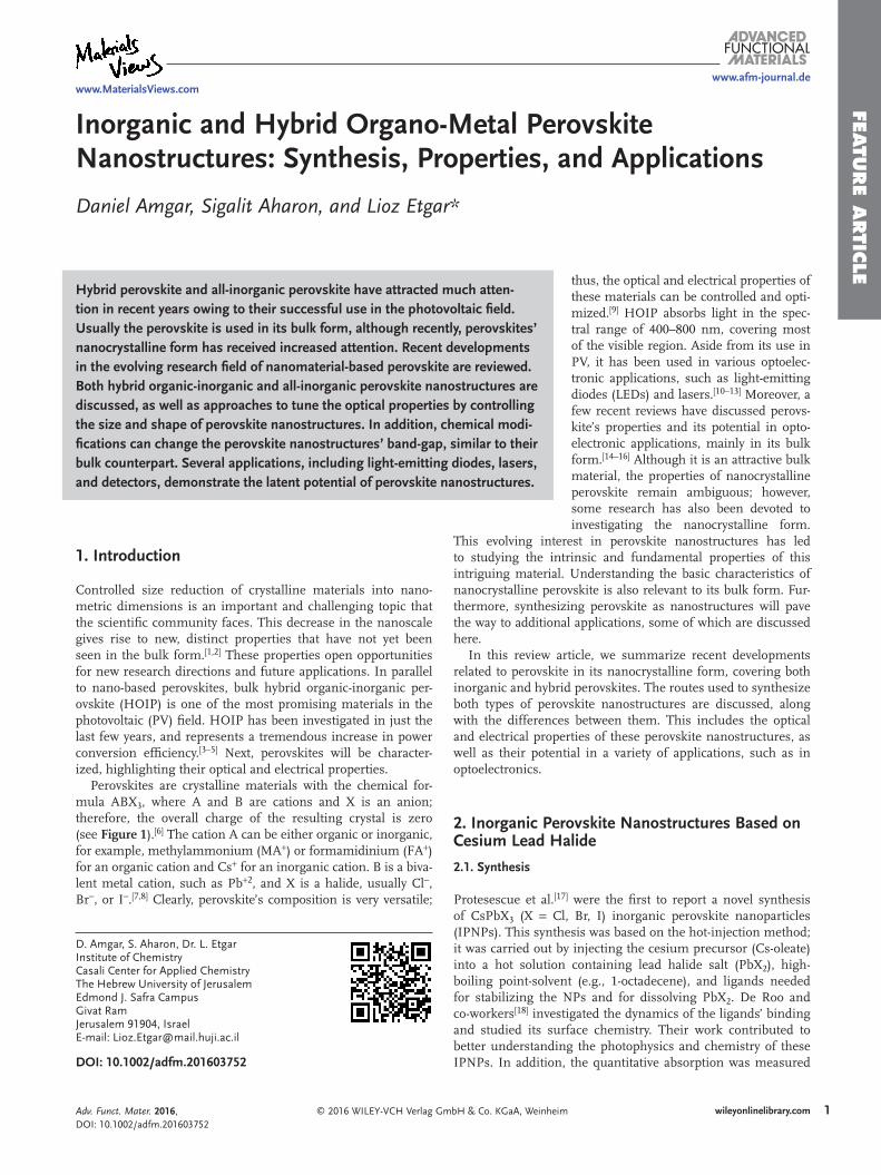
were used in the analysis (see Figure 4a–h). The size distribution of both CsPbBr3 and CsPbI3 were examined at growth durations of 1 s, 4 s, 20 s, and 40 s, resulting in different tendencies. The size distribution of CsPbBr3 NPs showed a trend of defocusing from the beginning, whereas with CsPbI3, the size distribu-tion exhibited a focusing step in the first 20 s of growth, fol-lowed by defocusing over longer growth periods. This study suggests using a kinetic model of the NPs’ growth, as described in Figure 4i. Based on the kinetic model, the monomers in the CsPbBr3 NP synthesis were depleted faster than the monomers in the CsPbI3 synthesis. Accordingly, small particles of CsPbBr3 never reach the critical radius of nucleation (owing to the faster diffusion of the bromide-based monomers), and therefore, they broaden the size distribution. On the other hand, the mono-mers of the CsPbI3 NP synthesis are diffused more slowly and can nucleate, expressed as a focusing step. Better understanding the kinetics of IPNPs provides an efficient and simple path to generate uniform NPs with narrow size distributions.
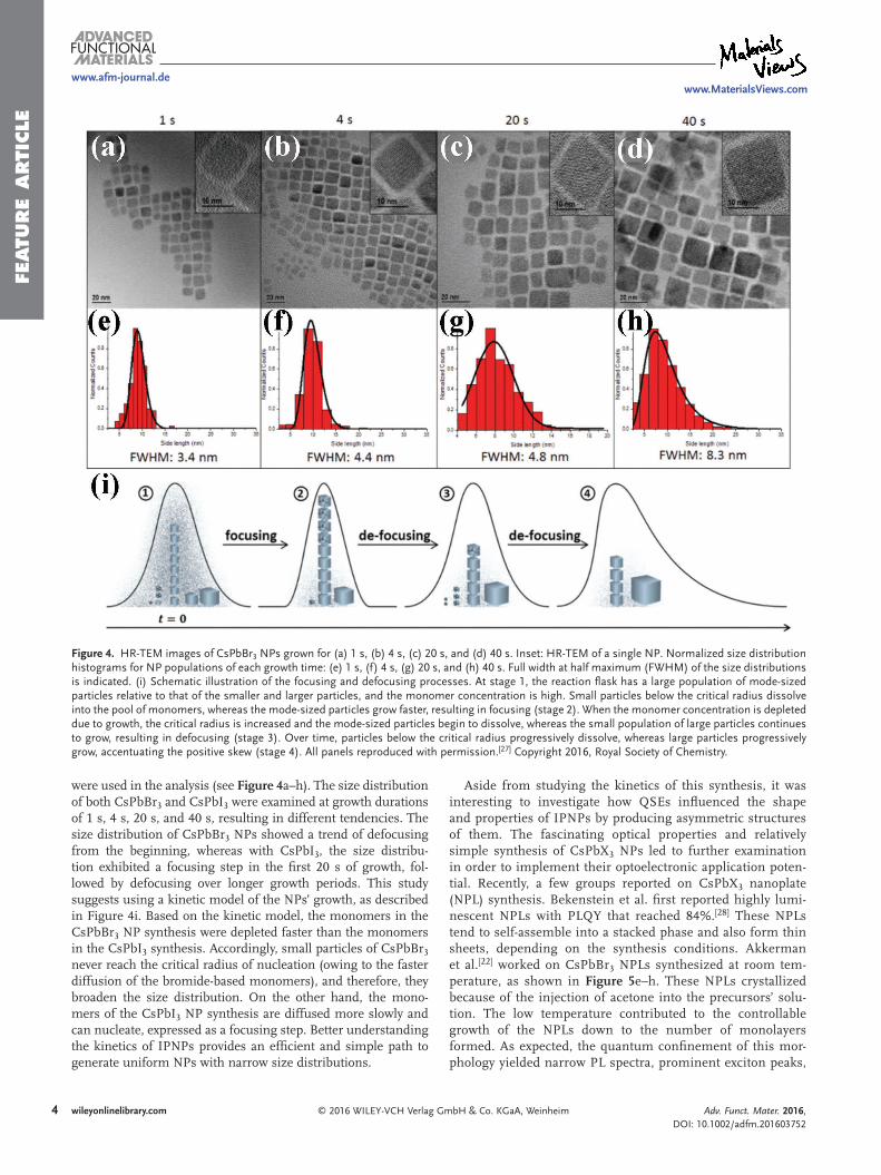
Aside from studying the kinetics of this synthesis, it was interesting to investigate how QSEs influenced the shape and properties of IPNPs by producing asymmetric structures of them. The fascinating optical properties and relatively simple synthesis of CsPbX3 NPs led to further examination in order to implement their optoelectronic application poten-tial. Recently, a few groups reported on CsPbX3 nanoplate (NPL) synthesis. Bekenstein et al. first reported highly lumi-nescent NPLs with PLQY that reached 84%.[28] These NPLs tend to self-assemble into a stacked phase and also form thin sheets, depending on the synthesis conditions. Akkerman et al.[22] worked on CsPbBr3 NPLs synthesized at room tem-perature, as shown in Figure 5e–h. These NPLs crystallized because of the injection of acetone into the precursors’ solu-tion. The low temperature contributed to the controllable growth of the NPLs down to the number of monolayers formed. As expected, the quantum confinement of this mor-phology yielded narrow PL spectra, prominent exciton peaks,
Adv. Funct. Mater. 2016, DOI: 10.1002/adfm.201603752
www.afm-journal.dewww.MaterialsViews.com
Figure 4. HR-TEM images of CsPbBr3 NPs grown for (a) 1 s, (b) 4 s, (c) 20 s, and (d) 40 s. Inset: HR-TEM of a single NP. Normalized size distribution histograms for NP populations of each growth time: (e) 1 s, (f) 4 s, (g) 20 s, and (h) 40 s. Full width at half maximum (FWHM) of the size distributions is indicated. (i) Schematic illustration of the focusing and defocusing processes. At stage 1, the reaction flask has a large population of mode-sized particles relative to that of the smaller and larger particles, and the monomer concentration is high. Small particles below the critical radius dissolve into the pool of monomers, whereas the mode-sized particles grow faster, resulting in focusing (stage 2). When the monomer concentration is depleted due to growth, the critical radius is increased and the mode-sized particles begin to dissolve, whereas the small population of large particles continues to grow, resulting in defocusing (stage 3). Over time, particles below the critical radius progressively dissolve, whereas large particles progressively grow, accentuating the positive skew (stage 4). All panels reproduced with permission.[27] Copyright 2016, Royal Society of Chemistry.
FEATU
RE A
RTIC
LE
5wileyonlinelibrary.com© 2016 WILEY-VCH Verlag GmbH & Co. KGaA, Weinheim
and a pronounced blue shift of the band-gap relative to bulk CsPbBr3.
Furthermore, several groups reported additional morpholo-gies through synthesis modifications, producing CsPbX3 nanowires (NWs) (seen in Figure 5a–d) as well as nanosheets, with superior optical properties for use of optoelectronic mate-rials in future applications.[24,29–33] The advantage of synthe-sizing various morphologies of nanostructures is mainly due to their high surface-to-volume ratio and anisotropy, particularly enhanced in NWs and nanorods.
2.2. Optical Properties
As mentioned previously, IPNPs are known for their efficient tunable optical properties. The band-gap tuning can result from compositional modifications or quantum confinement via size and shape modifications. For instance, substituting cations (FA instead of MA or Sn instead of Pb) was investigated for HOIPs.[19] Recently, Akkerman and co-workers extensively studied halide-exchange reactions by using a variety of halide precursors, such as octadecylamine-halide (ODA-X) and PbX2, as seen in Figure 6a.[19] The efficient exchangeable nature of the halides in this system derives from their high ion mobility and rapid diffusion in solution. The optical tuning across the visible, from green-emitting NPs to blue- or red-emitting NPs, was simply produced by mixing IPNPs with halide precursors (Figure 6b). The mixing reactions resulted in compositional homogenization, which led to intermediate optical features. Apparently, while using tetrabutylammonium-halides (TBA-X), the routes for halide exchange were restricted to specific direc-tions, from Br− to Cl− and from I− to Br−. The reverse routes did not work owing to hard/soft acid/base reactions. For example, TBA is a soft acid that prefers to bind to softer halide ions. Thus, Cl− from CsPbCl3 will not be exchanged with Br− from TBA-Br because Br− is softer than Cl− and prefers to remain bound to TBA. The halide-exchange reactions led to a blue or red shift in the optical features, verifying that the new halides were integrated into the crystal structure (Figure 6b). Figure 6c
presents the change in the band-gap as a function of the molar ratio between the added halide and the starting Br, showing the gradual replacement of the halide content. Figure 6d shows PLQY throughout the exchange process and the approximate matching of exchanged NPs and the NPs from direct synthesis. Furthermore, it is important to note that methylammonium-halides (MA-X) constitute problematic halide sources because of the possibility of a cation exchange between the Cs+ ions and the MA+ ions.[19] Halide-exchange processes were further dem-onstrated by other groups as well.[20,34] Kamat et al. reported on sintered IPNP solids with tunable optical features through halide-exchange reactions. The significance of this work is highlighted by its offering a proper solution for the instability of cubic phase CsPbI3 film, starting with a sintered CsPbBr3 film and then converting it into stable CsPbI3.[34]
Hu and co-workers investigated IPNPs as single photon emitters, demonstrating the superior optical properties of this material using absorption cross sections and lifetime meas-urements.[35] The intriguing optical features of IPNPs stimu-lated the search for further knowledge about their intrinsic spectral and dynamic mechanisms. Makarov et al. investi-gated these aspects comprehensively, focusing on single and multiexciton states in IPNPs. This analysis included measure-ments of exciton radiative lifetimes, rates of intraband cooling, the strength of exciton-exciton coupling, and non-radiative Auger recombination. The latter proved to be very efficient in IPNPs; however, it was detrimental to potential applications involving emissive optoelectronics. This study emphasized significant similarities in the spectroscopic properties between IPNPs and known semiconducting quantum dots (QDs), such as PbSe and CdSe. For instance, two similarities are the extremely short biexciton Auger lifetimes (Figure 7) and the absorption cross-sections, which were linearly dependent on the volume of the NP. Another observation was the formation of charged excitons (trions), decaying by the Auger mecha-nism. Moreover, the measured binding energy of biexcitons was stated as approximately 10 meV, again, similar to other QD systems.[36] A few other groups have investigated related mechanisms.[37–39]
Adv. Funct. Mater. 2016, DOI: 10.1002/adfm.201603752
www.afm-journal.dewww.MaterialsViews.com
Figure 5. TEM images of CsPbX3 NWs with various degrees of conversion with (a) chloride and (b) iodide anions. The insets show the evolution of emission color (UV excitation, λ = 365 nm) upon forming mixed-halide CsPb(Br/Cl)3 and CsPb(Br/I)3 NWs. HRTEM images of (c) Cl- and (d) I-exchange NWs. (e) TEM images of CsPbBr3 NPLs at low concentrations and (f) high concentrations. HRTEM images of NPLs (g) in a top view and (h) in stacks. (a–d) were reproduced with permission.[30] Copyright 2015, American Chemical Society. (e–h) were reproduced with permission.[22] Copyright 2016, American Chemical Society.

FEATU
RE
ARTI
CLE
6 wileyonlinelibrary.com © 2016 WILEY-VCH Verlag GmbH & Co. KGaA, Weinheim
An interesting work was reported by Seth et al.[40]; they revealed fluorescence blinking in the microsecond time scale and photoinduced emission enhancement for CsPbBr3 and CsPbBr2I NPs, which provide insight into the radiative and nonradiative deactivation pathways. Moreover, Raino and co-workers[41] described IPNPs’ highly stable narrow emissions with reduced blinking. The significance in this work lies in the outstanding single-photon radiative decay of 250 ps, which was highly accelerated compared with other emitting NPs.
The PLQY of IPNPs reached exceptionally high values, ≈90%. Wu and co-workers[42] investigated the origins of the
outstanding PLQY values by studying the dynamics of the carriers’ trapping and recombination mechanisms within CsPbBr3 IPNPs using transient absorption (TA) spectroscopy. The charge transfer to charge acceptors was also investigated, as presented in Figure 8a. The main explanation for the high PLQY value is the negligible traps of electrons and holes, resulting in non-radiative decay. It was also attributed to the efficient dissociation of excitons in the presence of hole or elec-tron acceptors, such as phenothiazine (PTZ) and benzoquinone (BQ), respectively. TEM analysis revealed that the IPNPs had a short edge of ≈6 nm, which is much smaller than the bulk Bohr exciton diameter (≈7.4 nm), thus creating quantum confine-ment. Therefore, discrete electron and hole levels are formed and the optically allowed charge transitions between them lead to discrete absorption bands in the absorption spectrum. The potentials of the lowest electron and hole levels were estimated to be ≈3.62 eV and 6.36 eV relative to the vacuum level, respec-tively. Using pump-probe TA measurements, CsPbBr3 NPs were excited and the induced changes were recorded versus wavelength and time. Figure 8b shows the exciton bleach (XB) feature, which can be attributed to the state-filling-induced bleach and exciton absorption (XA) feature, which in turn, can be attributed to the hot-exciton-induced red shift of the lowest energy excitonic band (X1). The transfer of electrons to an electron acceptor indicated that the state filling of the hole and electron levels were 32.8% and 67.2% of the XB feature, respectively. The valence band is more degenerated than the conduction band is, which may explain the larger contribu-tion of the electrons to the XB feature. Figure 8c presents the kinetics of the transient features; the time constant of the XB feature was 4.5 ± 0.2 ns. Complexes of CsPbBr3-BQ/PTZ were used to measure the rates of electron transfer (ET) and hole transfer (HT) from photoexcited CsPbBr3. For ET, the half-lives and recombination were found to be 65 ± 5 ps and 2.6 ± 0.4 ns,
Adv. Funct. Mater. 2016, DOI: 10.1002/adfm.201603752
www.afm-journal.dewww.MaterialsViews.com
Figure 6. (a) Overview of the different routes and precursors for the anion exchange reactions on CsPbX3 (X = Cl, Br, I) NPs reported here. (b) PL spectra of the CsPb(Br:X)3 (X = Cl, I) NPs prepared by anion exchange from CsPbBr3 NPs. (c) PL calibration curves: targeted emission energy could be obtained by adding a precise amount of halide precursor to a crude solution of CsPbBr3 NPs. The curves are reported as a function of the molar ratio between the added halide (or exchange halide) and the Br amount in the starting NPs. (d) PLQY recorded on the exchanged NPs (dots) as well as on the directly synthesized NPs (stars). Reproduced with permission.[19] Copyright 2015, American Chemical Society.
Figure 7. Auger recombination dynamics in perovskite QDs. This rep-resentation helps highlight the early stage short-lived PL component owing to biexcitons (characteristic time τ2X), which emerges at higher pump intensities. Symbols A and B denote the amplitudes of the total PL signal and its single-exciton component, whereas M = A − B denotes the amplitude of the multiexciton signal. Reproduced with permission.[36] Copyright 2016, American Chemical Society.

FEATU
RE A
RTIC
LE
7wileyonlinelibrary.com© 2016 WILEY-VCH Verlag GmbH & Co. KGaA, Weinheim
respectively. For HT, it was 49 ± 6 ps and 1.0 ± 0.2 ns, respec-tively. The absence of trap states and rapid interfacial ET and HT represent the most logical explanation for the unique PLQY. These findings may also be the key for the required photo physical understanding related to the charge separation phenomenon in solar applications and for future development of emissive devices.
A later work, by Swarnkar and co-workers,[43] focusing on the abnormal luminescence of IPNPs, provided new insights about the intrinsic optical features, and emphasized the advantages of IPNPs beyond traditional semiconducting QDs. The intense optical features of traditional colloidal QDs are associated with quantum confinement of charge carriers, thus enhancing the probability for transition. However, this characteristic leads to a broad size distribution and to numerous trap state issues. Accordingly, light properties, such as PLQY, are affected by self-absorption and Förster resonance electron transfer (FRET) mechanisms; thus, they change with the concentration of the NPs. Another typical disadvantage of using common QDs with LED devices is their temperature instability. An increase in temperature can induce a reduction of the band-gap, which consequently can cause color changes in the LED devices. This work highlights the valuable optical advantages of IPNPs, both as ensembles and single-crystals, in overcoming the above defi-ciencies. The PLQY of IPNPs could reach 90%, showing sup-pressed PL blinking. Regarding the temperature challenge, the PL of IPNPs did not change with temperature, when meas-ured in the range of 25 to 100 °C. In addition, a single and an ensemble of IPNPs exhibit almost the same spectral gap, indi-cating no additional PL broadening, self-absorption, and FRET issues, which were discussed before. Furthermore, polarized
emission was observed for the first time,[44] with polarization values of 0.36 and 0.40, associated with CsPbI3, in solution and as a film, respectively.
Energy transfer between colloidal CsPbBr3 NPs was also recently demonstrated.[45] The energy transfer process was driven by concentration and by band-gap differences, moving from the smaller to the larger NP (Figure 9). The proximity of the colloidal NPs enabled energy transfer processes to occur, and enhancement of the ET was observed after a few hours, after which the NPs could settle in their positions. PL measure-ments revealed a shift, where the PL wavelength changed from the small NPs to the larger NPs. In addition, where mixing of sizes was present in the sample, a shoulder appeared, indi-cating different NP sizes in the sample. Next, various applica-tions of IPNPs with regard to LEDs will be discussed.
2.3. Applications
2.3.1. CsPbX3 NPs for Light-Emitting Diodes (LEDs)
The excellent optical properties of IPNPs, including sharp emissions and high PLQY values, revealed their huge potential as light-emitting materials in a variety of optoelectronic appli-cations, such as LEDs and lasers. Song et al.[46] were the first to report CsPbX3 NP-based LEDs that produced an external quantum efficiency (EQE) of 0.07%, 0.09%, and 0.12% for three LEDs with different halide contents (blue, orange, and green devices, respectively; NP-based LEDs are presented in Figure 10c–e, as well as the corresponding electrolumines-cence (EL) spectra). The devices have the following layered
Adv. Funct. Mater. 2016, DOI: 10.1002/adfm.201603752
www.afm-journal.dewww.MaterialsViews.com
Figure 8. (a) Schematic energy level diagram of CsPbBr3 quantum dot (QD)−benzoquinone (BQ) and QD−phenothiazine (PTZ(complexes and pos-sible charge separation and recombination pathways)). The black solid lines denote the lowest energy electron and hole levels in QDs. The thick gray lines denote the lowest unoccupied molecular orbitals (LUMOs) and the highest occupied molecular orbitals (HOMOs) of the BQ and PTZ molecules. Forward charge separation processes, including electron transfer (ET) to BQ and hole transfer (HT) to PTZ, are denoted by blue arrows, and backward charge recombination processes are denoted by red arrows. Electron−hole recombination inside the QD is denoted by a red wavy arrow. (b) Transient spectra of QDs at the indicated delay time from 0.2 ps to 20 ns. Exciton bleach (XB) and photoinduced absorption (PA) features are labeled. (c) Kinetics of XB (blue triangles, reduced by a factor of 24 and inverted), PA (red circles), and PL decay (green squares) of QDs. The black solid lines are multi-exponential fits to this kinetics. Reproduced with permission.[42] Copyright 2015, American Chemical Society.

FEATU
RE
ARTI
CLE
8 wileyonlinelibrary.com © 2016 WILEY-VCH Verlag GmbH & Co. KGaA, Weinheim
structure: indium tin oxide (ITO)/poly(ethylenedioxithiophene): polystyrene (PEDOT:PSS)/poly(9-vinlycarbazole) (PVK)/ CsPbX3 NPs/ 2,2′,2″-(1,3,5-Benzinetriyl)-tris(1-phenyl-1-H-benzimidazole) (TPBi)/ LiF/Al. TPBi thin films were employed as an electron transporting layer and PVK served as the hole conductor and electron blocking layer, thus encouraging the electrons and holes to recombine in the NP layer. The device’s structure and energy diagram are presented in Figure 10a,b. Following this work, several other studies have been conducted in this direction.[47–53] In this context, Kim and co-workers reported on IPNP solids that can be utilized for LEDs and other optoelectronic applications. IPNPs were fabricated using a cen-trifugal casting process that combined both purification and deposition of IPNPs on a desired substrate. The obtained layer was highly homogenous and the thickness could be controlled by the ratio between the crude NPs and the anti-solvent in the
centrifuge tube. This process may have potential in future opto-electronic applications, such as for forming a uniform layer of IPNP-based emitters.[54]
Palazon et al.[55] reported polymer-free films of CsPbX3 NPs as a UV-to-white color-conversion layer in LEDs, using X-ray treatment that inhibits halide exchange processes. The X-ray treatment enabled the formation of a bi-layer of CsPbBr3 and CsPbI3 with individual emissions, thus preventing their compo-sitional homogenization. The effect of X-ray irradiation was fur-ther implemented for lithographic processes on IPNPs films.[56]
A recent work by Huang and co-workers[57] described the synthesis of water-resistant IPNPs with a polyhedral oligomeric silsesquioxane (POSS) capping agent and the subsequent utili-zation of these stable NPs in white LEDs. This NP protection prevents the rapid halide exchange process in solution and in the solid state, which enables the desired optical character-istics to be preserved. Taking the color stability into account, down-conversion white LEDs were fabricated using Br- and I-based POSS-IPNPs as powders, achieving 14.1 lm W−1 luminance efficiency. For future development, QY must be increased from the present value of 45% up to 70% in order to achieve the commercial requirement of phosphors.
2.3.2. CsPbX3 NPs as Lasers
CsPbX3 NPs have become appropriate candidates for opto-electronics thanks to their enhanced optical properties, such as high stability, low cost, simple synthesis, and tunable low excitation threshold emission. Eaton et al.[32] recently reported a new method of synthesizing CsPbX3 NWs and demonstrated their virtues as efficient lasers. This was the first time that sur-factant-free CsPbX3 NWs were synthesized with diameters suit-able for photonic NW lasing (higher than ≈180 nm). CsPbBr3 NW lasers have been shown to lase for more than 109 excita-tion cycles, presenting high stability while lasing even under ambient conditions. The NWs had the technical characteristics required to act as both a gain medium and a laser cavity. Fur-thermore, it was shown that above their threshold, the NWs stimulated emission that was increased with their excitation intensity, as demonstrated in Figure 11. Additional groups also studied the lasing potential of IPNPs.[58–60] Xu et al.[61]
Adv. Funct. Mater. 2016, DOI: 10.1002/adfm.201603752
www.afm-journal.dewww.MaterialsViews.com
Figure 9. Schematic illustration of the energy transfer process involving CsPbBr3 NPs. Reproduced with permission[45] Copyright 2016, American Chemical Society.
Figure 10. (a) Illustration of the structure of multilayer perovskite QD-based LED (QLED) device. b) Flat-band energy level diagram. (c–e) Illustrations of QLED devices with the Nanjing University of Science and Technology (NUST) logo. f) The EL spectra (straight line) of a sample shown in (c–e) under an applied voltage of 5.5 V, and the PL spectra (dashed line) of NPs dispersed in hexane. Reproduced with permission.[46] Copyright 2015, Wiley-VCH.

FEATU
RE A
RTIC
LE
9wileyonlinelibrary.com© 2016 WILEY-VCH Verlag GmbH & Co. KGaA, Weinheim
investigated CsPbBr3 NPs that exhibit two-photon-pumped lasing with an exceptionally low threshold when coupled with microtubule resonators.
2.3.3. CsPbX3 NPs as Photodetectors
Additional research introduced the use of IPNPs as spectro-chemical probes and halide reservoirs in catalysis. As men-tioned, the halide content in perovskite NPs can be altered by simple halide-exchange reactions. This exchangeable nature gave rise to possible applications in organo-halide chemistry, as shown in Figure 12. It was suggested that IPNPs react as a catalytic reservoir for a Finkelstein exchange reaction between IPNPs and organo-halides, which is of major importance in various synthetic reactions and in the colorimetric assay of free ions in solution. The IPNPs that participate in the reaction exist in high concentrations and have high solubility to enable the halides to directly catalyze the reaction. A PL test was per-formed to validate the halide reservoir role of the NPs, and indeed, a change in PL was observed, confirming the change in the halide content within the CsPbX3 lattice. In general, the IPNP features controlled the reaction kinetics in real time, via a colorimetric response in a simple and efficient manner.[62]
One of the pioneering works that used CsPbI3 as photode-tectors was reported by Ramasamy et al.[63] In this work, the possibility of tuning the IPNPs’ optical properties by forward and reverse anion-exchange reactions was demonstrated. Red-emitting CsPbI3 NPs were used in a photodetector device due to their relatively longer radiative lifetime than the green- and blue-emitting NPs. The photodetector structure
Adv. Funct. Mater. 2016, DOI: 10.1002/adfm.201603752
www.afm-journal.dewww.MaterialsViews.com
Figure 11. Lasing in single-crystal CsPbBr3 nanowires. (a) Dark-field image of a CsPbBr3 nanowire. (b–d) Nanowire (a) under excitation from a femtosecond pulsed laser with increasing excitation fluency. (Scale bar, 2 μm) Reproduced with permission.[32] Copyright 2016, National Academy of Science.
Figure 12. Schematic illustration of CsPbX3 NPs as halide reservoirs and colorimetric probes. The NPs are a halide source in Finkelstein reactions of organo-bromides. (a) CsPbI3 are exchanged with organic bromides, forming organo-iodides and CsPbBr3. (b) In addition, a similar reactivity is used to assay organo-halide-based chemical reactions, where Br−, released during the course of a reaction, can be observed by the colorimetric change in the perovskite NPs. Reproduced with permission.[62] Copyright 2016, Wiley-VCH.

FEATU
RE
ARTI
CLE
10 wileyonlinelibrary.com © 2016 WILEY-VCH Verlag GmbH & Co. KGaA, Weinheim
is shown in Figure 13a, where CsPbI3 NPs were drop casted on a Si substrate with pre-patterned gold electrodes and later annealed at 200 °C for 30 min in a N2 atmosphere. The photo-current was increased by several orders of magnitude of the light intensity (Figure 13b); therefore, the photosensitivity, which is defined as the ratio of photocurrent to dark current (Iph/Idark), was exceedingly good (105). The response of the photocurrent to the light intensity is shown in Figure 13c; the fitting of this response is consistent with different applied biases. Figure 13d shows the spectral response of the photo-current, which closely follows the absorption spectrum of CsPbI3. The photocurrent time, measured in the dark and
under illumination, is presented in Figure 13e, exhibiting a reproducible response to ON–OFF cycles, whereas rapid rise and decay times can be seen in Figure 13f for this photode-tector device.
An additional interesting work was reported by Li et al.[64] using the IPNPs in planar photodetectors. A recyclable disso-lution–recrystallization process was conducted on the IPNPs, creating crack-free surfaces made at room temperature. Using this strategy, planar photodetectors were fabricated, as can be seen in Figures 14a+b. The charge transport was difficult for the untreated film, as can be seen in Figure 14a, whereas it was much improved for the treated film (Figure 14b). Figure 14c+d
Adv. Funct. Mater. 2016, DOI: 10.1002/adfm.201603752
www.afm-journal.dewww.MaterialsViews.com
Figure 13. (a) Schematic of the CsPbI3 NCs photodetector (L = 3 mm, W = 7800 mm). (b) I–V characteristics of close-packed CsPbI3 NC films as a function of incident light intensity. (c) Dependence of the photocurrent on the light intensity at different applied biases. (d) Absorption and spectral dependence of the photocurrent measured at 1 V bias. (e) Photocurrent–time (Iph–t) response measured in the dark and under illumination using a laser diode at 405 nm as a function of an applied bias at a fixed light intensity (Pin = 1.98 mW cm2). (f) Rise and decay times of the photodetector device. Reproduced with permission.[63] Copyright 2016, American Chemical Society.

FEATU
RE A
RTIC
LE
11wileyonlinelibrary.com© 2016 WILEY-VCH Verlag GmbH & Co. KGaA, Weinheim
show the increased response of more than sevenfold for the treated photodetectors compared with the untreated ones under 10 V bias. The EQE, which is an important factor, indicated that the efficiency of the photogenerated carriers was also improved, as can be seen in Figure 14 e+f, for the untreated and treated films, respectively. The maximum EQE value reached 41% at 10 V, which is much higher than that of the untreated device, which is less than 6%. The main reason for these differences is due to the loss of photogenerated carriers from scattering and recombination.
Next, hybrid organic-inorganic perovskite nanostructures will be discussed.
3. Hybrid Organic-Inorganic Lead Halide Perovskite Nanostructures
In parallel to works discussing IPNPs, a growing number of reports have discussed hybrid organic-inorganic perovs-kite nanostructures. Two main fundamental differences arise when discussing the synthesis and properties of all-inorganic perovskite nanostructures compared with hybrid perovskite nanostructures. First, when synthesizing hybrid perovskite with organic cations instead of inorganic ones, the possibility of band-gap tuning increases, reaching longer wavelengths of ≈800 nm (compared with ≈700 nm wavelength with the
Adv. Funct. Mater. 2016, DOI: 10.1002/adfm.201603752
www.afm-journal.dewww.MaterialsViews.com
Figure 14. Photoresponse of all-inorganic pervoskite films before and after RDR healing. Schematic diagram showing the device’s structure of CsPbBr3 NCs (a) before and (b) after treatment. (c,d) Response and (e,f) EQE spectra of the PDs based on untreated and treated CsPbBr3 films under different biases, respectively. Reproduced with permission.[64] Copyright 2016, American Chemical Society.

FEATU
RE
ARTI
CLE
12 wileyonlinelibrary.com © 2016 WILEY-VCH Verlag GmbH & Co. KGaA, Weinheim Adv. Funct. Mater. 2016, DOI: 10.1002/adfm.201603752
www.afm-journal.dewww.MaterialsViews.com
inorganic perovskite nanostructures).[65] In addition, the organic cation limits the synthesis temperature, permits high precursors to be soluble, and allows a standard atmosphere of humidity and oxygen during the synthesis, as described next.
3.1. Synthesis of HOIP NPs
Pioneering work in this field was done by Schmidt et al.,[66] who demonstrated the synthesis of CH3NH3PbBr3 NPs (see Figure 15) by injecting methyl ammonium bromide (MABr) and PbBr2 solutions into a preheated reaction medium of oleic acid (OAc) and octyl ammonium bromide (OABr) dissolved in octadecene. In the next step, the particles were precipitated by adding acetone, followed by centrifugation. These particles (dis-persed in toluene) exhibited a PLQY of ≈20% as well as good stability (longer than three months).
Following this work, Zhang et al.[65] developed a ligand-assisted re-precipitation strategy for fabricating brightly lumi-nescent and color-tunable colloidal CH3NH3PbX3 (X = Cl−, Br−, I−) NPs. This synthesis included a dropwise injection of a solution of precursors in DMF (the precursors included PbX2, MAX, and n-octylamine) into toluene while vigorously stirring the reaction medium. These NPs exhibited absolute PLQY up to 70%. The halides’ composition changed the optical properties as the PL wavelength was altered in the range of 405–730 nm for the various halide compositions (Figure 16). In this work the use of these NPs in white LEDs was also demonstrated.
In HOIP the organic cation plays an important role. Using a long-chain organic cation that cannot be introduced into the perovskite structure will result in reduced dimensionality of the perovskite structure.[67] Dou et al.[68] synthesized a single crystalline 2D hybrid perovskite using C4H9NH3 as the organic cation and Br as the halide. The long organic cation results in well-defined square shaped plates, which leads to a shift in the band-gap of the material. In another work,[69] broad spec-tral tunability was achieved by changing the composition of the methyl and octlyammonium cations in colloidal synthesis. By increasing the octlyammonium cation, 2D perovskites were formed with a platelet nature; however, their emission was lower than the 3D perovskite.
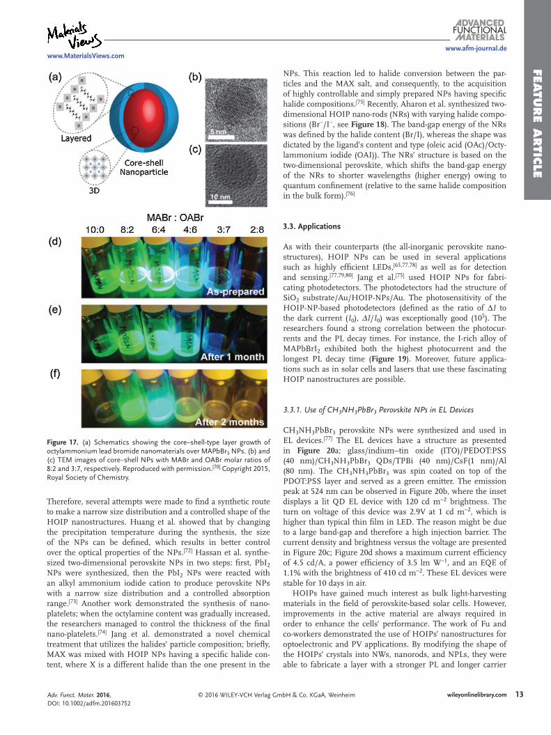
Keeping in mind the role of the cation in these HOIP NPs, the synthesis of the solution-processed core-shell type mixed with methylammonium–octylammonium, leading to bromide
perovskite NPs was demonstrated.[70] The NPs’ size ranged between 5 and 12 nm with a spherical shape and tunable optical proper-ties. The core-shell-type NPs exhibited PLQY up to 92%. The ratio of the cations in the precursor solution is the factor that controls the growth layer and the stability of these NPs. The reported core-shell-type structure, comprising a shell, consists of high band-gap 2D perovskite (C8H17NH3)2(CH3NH3)x –1 PbxBr3x+1 (x = 1, 2, 3,…) over a low band-gap MAPbBr3 core, as shown in Figure 17a. Figures 17b+c present TEM images of the mixed organo-lead bromide NPs obtained from cation ratios of 8:2 and 3:7, respectively.
One of the disadvantages of the HOIP NPs is their instability in polar solvents. In order to overcome this problem, Vybornyi et al.[71] synthesized CH3NH3PbBr3 NPs without using a polar solvent. The reaction between PbX2 and the methylamine was conducted using a high boiling point, nonpolar solvent with the ligands present in the solution. A PLQY of 15–50% was demon-strated with amplified spontaneous emission from thin films of green-emitting CH3NH3PbBr3 NWs.
3.2. Size and Shape Control of HOIP NPs
The synthetic routes of the HOIP NPs, as previously described, have two problematic aspects: (1) the size distribution of the NPs is wideand (2) the shape of the NPs is hard to define.
Figure 15. HRTEM image of an isolated perovskite nanoparticle (scale bar = 2 nm) and a schematic representation of an array of corner-sharing MX6 octahedra confined to the three dimensions owing to the organic capping. Reproduced with permission.[66] Copyright 2016, Wiley-VCH.
Figure 16. (a) Optical images of CH3NH3PbX3 QDs (nos. 1–9) under ambient light and a 365 nm UV lamp. (b) PL emission spectra of CH3NH3PbX3 QDs. Reproduced with permission.[65] Copyright 2016, Royal Society of Chemistry.
FEATU
RE A
RTIC
LE
13wileyonlinelibrary.com© 2016 WILEY-VCH Verlag GmbH & Co. KGaA, WeinheimAdv. Funct. Mater. 2016, DOI: 10.1002/adfm.201603752
www.afm-journal.dewww.MaterialsViews.com
Therefore, several attempts were made to find a synthetic route to make a narrow size distribution and a controlled shape of the HOIP nanostructures. Huang et al. showed that by changing the precipitation temperature during the synthesis, the size of the NPs can be defined, which results in better control over the optical properties of the NPs.[72] Hassan et al. synthe-sized two-dimensional perovskite NPs in two steps: first, PbI2 NPs were synthesized, then the PbI2 NPs were reacted with an alkyl ammonium iodide cation to produce perovskite NPs with a narrow size distribution and a controlled absorption range.[73] Another work demonstrated the synthesis of nano-platelets; when the octylamine content was gradually increased, the researchers managed to control the thickness of the final nano-platelets.[74] Jang et al. demonstrated a novel chemical treatment that utilizes the halides’ particle composition; briefly, MAX was mixed with HOIP NPs having a specific halide con-tent, where X is a different halide than the one present in the
NPs. This reaction led to halide conversion between the par-ticles and the MAX salt, and consequently, to the acquisition of highly controllable and simply prepared NPs having specific halide compositions.[75] Recently, Aharon et al. synthesized two-dimensional HOIP nano-rods (NRs) with varying halide compo-sitions (Br−/I−, see Figure 18). The band-gap energy of the NRs was defined by the halide content (Br/I), whereas the shape was dictated by the ligand’s content and type (oleic acid (OAc)/Octy-lammonium iodide (OAI)). The NRs’ structure is based on the two-dimensional perovskite, which shifts the band-gap energy of the NRs to shorter wavelengths (higher energy) owing to quantum confinement (relative to the same halide composition in the bulk form).[76]
3.3. Applications
As with their counterparts (the all-inorganic perovskite nano-structures), HOIP NPs can be used in several applications such as highly efficient LEDs,[65,77,78] as well as for detection and sensing.[77,79,80] Jang et al.[75] used HOIP NPs for fabri-cating photodetectors. The photodetectors had the structure of SiO2 substrate/Au/HOIP-NPs/Au. The photosensitivity of the HOIP-NP-based photodetectors (defined as the ratio of ΔI to the dark current (I0), ΔI/I0) was exceptionally good (105). The researchers found a strong correlation between the photocur-rents and the PL decay times. For instance, the I-rich alloy of MAPbBrI2 exhibited both the highest photocurrent and the longest PL decay time (Figure 19). Moreover, future applica-tions such as in solar cells and lasers that use these fascinating HOIP nanostructures are possible.
3.3.1. Use of CH3NH3PbBr3 Perovskite NPs in EL Devices
CH3NH3PbBr3 perovskite NPs were synthesized and used in EL devices.[77] The EL devices have a structure as presented in Figure 20a; glass/indium−tin oxide (ITO)/PEDOT:PSS (40 nm)/CH3NH3PbBr3 QDs/TPBi (40 nm)/CsF(1 nm)/Al (80 nm). The CH3NH3PbBr3 was spin coated on top of the PDOT:PSS layer and served as a green emitter. The emission peak at 524 nm can be observed in Figure 20b, where the inset displays a lit QD EL device with 120 cd m−2 brightness. The turn on voltage of this device was 2.9V at 1 cd m−2, which is higher than typical thin film in LED. The reason might be due to a large band-gap and therefore a high injection barrier. The current density and brightness versus the voltage are presented in Figure 20c; Figure 20d shows a maximum current efficiency of 4.5 cd/A, a power efficiency of 3.5 lm W−1, and an EQE of 1.1% with the brightness of 410 cd m−2. These EL devices were stable for 10 days in air.
HOIPs have gained much interest as bulk light-harvesting materials in the field of perovskite-based solar cells. However, improvements in the active material are always required in order to enhance the cells’ performance. The work of Fu and co-workers demonstrated the use of HOIPs’ nanostructures for optoelectronic and PV applications. By modifying the shape of the HOIPs’ crystals into NWs, nanorods, and NPLs, they were able to fabricate a layer with a stronger PL and longer carrier
Figure 17. (a) Schematics showing the core–shell-type layer growth of octylammonium lead bromide nanomaterials over MAPbBr3 NPs. (b) and (c) TEM images of core–shell NPs with MABr and OABr molar ratios of 8:2 and 3:7, respectively. Reproduced with permission.[70] Copyright 2015, Royal Society of Chemistry.

FEATU
RE
ARTI
CLE
14 wileyonlinelibrary.com © 2016 WILEY-VCH Verlag GmbH & Co. KGaA, Weinheim Adv. Funct. Mater. 2016, DOI: 10.1002/adfm.201603752
www.afm-journal.dewww.MaterialsViews.com
lifetime, relative to the bulk form. The formation of the per-ovskite nanostructure-based layer was carried out using a disso-lution-recrystallization platform over spin-coated PbI2 (or lead acetate) film, shown in the scheme in Figure 21. The obtained single-crystal nanostructures were characterized via surface photovoltage measurements and identified as n-type semicon-ductors. Also reported was an interfacial conversion of the PbI2
film into a highly crystalline MAPbI3 layer (Figure 21) that can generate PV devices with high power conversion efficiency.[81]
The nanocrystalline form of HOIPs was found to have many advantages for optoelectronic applications, as mentioned pre-viously. In addition to LED, photodetection, and PV, HOIP nanostructures have another potential use as lasing materials. Zhu et al.[82] utilized the attractive physical properties for HOIP
Figure 18. TEM images and inset FFTs of NRs having various halide compositions. Reproduced with permission.[76] Copyright 2015, American Chem-ical Society.
Figure 19. (a) I−V characteristics of MAPbBr3 film under 365 and 505 nm irradiation (60 mW cm–2) and dark conditions. The SEM image shows the film deposited on Au electrodes with a 2 μm gap (inset). (b) I−t curves at a bias voltage of 2 V under chopped radiation. (c) I−V and (d) I−t curves of MAPbBrI2 film under 365 (60 mW cm–2), 505 (60 mW cm–2), and 617 nm (40 mW cm–2) irradiation and dark conditions. reproduced with permis-sion.[75] Copyright 2015, Wiley-VCH.

FEATU
RE A
RTIC
LE
15wileyonlinelibrary.com© 2016 WILEY-VCH Verlag GmbH & Co. KGaA, WeinheimAdv. Funct. Mater. 2016, DOI: 10.1002/adfm.201603752
www.afm-journal.dewww.MaterialsViews.com
NW-based lasers, synthesized by surface solution growth depo-sition at RT. The NWs’ length reached ≈20 μm and the NWs’ width reached a few hundred nm. The grown HOIP NWs had a RT tunable lasing with extremely low thresholds (220 nJ cm−2), corresponding to a low charge carrier density of 1.5 × 1016 cm−3. The minimal trap states of the charge carrier can be translated to an estimated PLQY that can reach 100%.
4. Conclusions and Outlook
We have summarized the main important contributions to the field of perovskite-based nanostructures. Perovskite nanostruc-tures have been recently reported and their outstanding optical and electronic properties have been under intense research as a result. We focused on IPNPs and on HOIP nanostructures, their interesting properties, and potential applications. We have discussed the synthetic methods of fabricating perovskite NPs (with inorganic and organic cations), as well as their optical and structural modification and characterization. Importantly, it was found that halide-exchange processes and QSEs are highly effective in both perovskites, enabling band-gap tuning across the visible spectrum, thus making them attractive for optoelec-tronic applications. Some reports demonstrated highly efficient LEDs and photodetectors based on perovskite NPs, whereas other reports described the sensing ability of these perovskite
NPs. The utilization of CsPbX3 IPNPs was also found to be applicable for lasing applications. Extremely high PLQY values, narrow emission peaks in the visible region, a tunable band-gap, and an additional degree of stability were reported, showing the potential of these nanostructures.
Looking forward, there are still many fundamental open questions regarding these interesting perovskite nanostruc-tures, in addition to new applications that have not yet been reported. Here, we discussed several key issues and chal-lenges, which should receive more attention in the future. First, a few improvements were recommended regarding the purification process of the NPs, affecting PLQY, to gen-erate high-quality perovskite NPs for electronic applications. Regarding this aspect, the stability (photo-stability, thermal stability, and chemical stability), especially related to HOIP NPs, needs to be improved in order to further utilize perovs-kite NPs in optoelectronic applications. Moreover, to date, there has been no efficient way to deposit these perovskite nanostructures as a conductive film with good transport prop-erties. The organic ligands protecting the perovskite nano-structures pose difficulties in their transport through the deposited film; therefore, establishing an efficient ligands exchange method is essential. Second, the bulk form of per-ovskite attained a revolutionary success as a light-absorbing material in solar cells, encouraging further investigation of the electronic properties of the nano-form in terms of energy
Figure 20. Characteristics of QD-LEDs. (a) Flat-band energy-level diagram of different layers of materials employed in QD-LED. The values of the energy levels are illustrated with respect to the vacuum level. (b) Comparison of normalized EL (solid red line) and PL (dashed blue line) spectra of CH3NH3PbBr3 QDs. The inset is an optical photograph of a lit QD-LED. (c) Current density (red) and brightness (blue) versus voltage characteristics. (d) Current, power efficiency, and EQE as a function of the brightness of the QD-LED. Reproduced with permission.[77] Copyright 2015, American Chemical Society.

FEATU
RE
ARTI
CLE
16 wileyonlinelibrary.com © 2016 WILEY-VCH Verlag GmbH & Co. KGaA, Weinheim Adv. Funct. Mater. 2016, DOI: 10.1002/adfm.201603752
www.afm-journal.dewww.MaterialsViews.com
transfer and band-gap engineering. In addition, Kamat et al.[34] suggested an approach to generate a bulk CsPbX3 film, starting from CsPbX3 NPs. This can pave additional path-ways for solar applications. Third, water-soluble IPNPs and HOIP NPs constitute an interesting research direction, since they would open the possibility for biological applications. It is known that perovskite is not stable in water; therefore, on the one hand, this task is very challenging, but on the other hand, it can open directions for new applications. In addition, in seeking novel functional materials, one of the interesting directions can be composite structures, such as hybrid and core-shell nanostructures, taking into account the similarity of perovskite NPs to other semiconducting QDs (PbS, CdSe, and others). This will open the possibility to extend the absorbance wavelength of these materials. Another motivation for using such hybrid composites is hidden in the PL stability of tradi-tional semiconducting QDs. For example, the need for core-shell structures is related to the enhancement of the optical properties, especially the radiative decays and lifetimes, which constitute a serious drawback of using traditional QDs. These optical parameters also influence the overall PLQY mostly affected by trap states at the surface. It was reported that per-ovskite nanostructures have negligible trapping at the sur-face due to rapid dissociation of the exciton in the presence of charge acceptors;[42,82] therefore, perovskite nanostructures might contribute in this direction. Ning et al.[83] reinforced the feasibility of fabricating the suggested hybrid nanostructures in terms of energetic considerations and crystallographic matching between the crystalline structure of PbS QDs and MAPbX3. The possibility of generating ‘dots-in-a-matrix’
crystals via epitaxial growth was presented and discussed, accompanied by density functional theory (DFT) calculations. The authors claimed that the dots inherit the crystalline align-ment of the perovskite. This work may inspire and open a new window to apply this system to core-shell nanocomposites of perovskite with known QDs. To do so, a better understanding and control of the surface chemistry of these NPs is required. In summary, we think that a fundamental understanding and implementation of these novel IPNPs and HOIP NPs is still lacking. An in-depth physical and chemical understanding of the underlying exciton, recombination, and PL mechanisms is needed and their thorough investigation is the main factor necessary for facilitating the functionalization and implemen-tation of these materials.
AcknowledgementsThe authors would like to acknowledge the financial support of the Israel Alternative Energy Foundation (I-SAEF) and the Tashtiot Project of the Office of the Chief Scientist.
Received: July 24, 2016Revised: September 7, 2016
Published online:
[1] M. C. Daniel, D. Astruc, Chem. Rev. 2004, 104, 293.[2] B. O. Dabbousi, J. Rodriguez-Viejo, F. V. Mikulec, J. R. Heine,
H. Mattoussi, R. Ober, K. F. Jensen, M. G. Bawendi, J. Phys. Chem. B 1997, 101, 9463.
Figure 21. Schematic illustration of the synthetic routes used to create both cubic-like grains and shape-modified nanocrystals of HOIPs as active layers in a solar cell. Reproduced with permission.[81] Copyright 2015, Wiley-VCH.

FEATU
RE A
RTIC
LE
17wileyonlinelibrary.com© 2016 WILEY-VCH Verlag GmbH & Co. KGaA, WeinheimAdv. Funct. Mater. 2016, DOI: 10.1002/adfm.201603752
www.afm-journal.dewww.MaterialsViews.com
[3] J. Burschka, N. Pellet, S.-J. Moon, R. Humphry-Baker, P. Gao, M. K. Nazeeruddin, M. Graetzel, Nature 2013, 499, 316.
[4] N. J. Jeon, J. H. Noh, W. S. Yang, Y. C. Kim, S. Ryu, J. Seo, S. I. Seok, Nature 2015, 517, 476.
[5] http://www.nrel.gov/ncpv/images/efficiency_chart.jpg 9/2016.[6] J. M. Frost, K. T. Butler, F. Brivio, C. H. Hendon, M. van Schilfgaarde,
A. Walsh, Nano Lett. 2014, 14, 2584.[7] J. W. Lee, D.-H. Kim, H.-S. Kim, S.-W. Seo, S. M. Cho, N. G. Park,
Adv. Energy Mater. 2015, 5, 1501310.[8] G. E. Eperon, S. D. Stranks, C. Menelaou, M. B. Johnston,
L. M. Herz, H. J. Snaith, Energy Environ. Sci. 2014, 7, 982.[9] J. L. Knutson, J. D. Martin, D. B. Mitzi, Inorg. Chem. 2005, 44, 4699.
[10] Z.-K. Tan, R. S. Moghaddam, M. L. Lai, P. Docampo, R. Higler, F. Deschler, M. Price, A. Sadhanala, L. M. Pazos, D. Credgington, F. Hanusch, T. Bein, H. J. Snaith, R. H. Friend, Nat. Technol. 2014, 9, 687.
[11] G. Xing, N. Mathews, S. S. Lim, N. Yantara, X. Liu, D. Sabba, M. Grätzel, S. Mhaisalkar, T. C. Sum, Nat. Mater. 2014, 13, 476.
[12] S. A. Veldhus, P. P. Boix, N. Yantara, M. Li, T. C. Sum, N. Mathews, S. G. Mhaisalkar, Adv. Mater. 2016, 28, 6804.
[13] S. Bai, Z. Yuan, F. Gao, J. Mater. Chem. C 2016, 4, 3898.[14] B. R. Sutherland, E. H. Sargent, Nat. Photon. 2016, 10, 295.[15] G. Yang, H. Zhong, Chin. Chem. Lett. 2016, doi:10.1016/j.
cclet.2016.06.047.[16] S. Gonzalez-Carrero, R. E. Galian, J. Pérez-Prieto, Opt. Express 2016,
24, A285.[17] L. Protesescue, S. Yakunin, M. I. Bodnarchuk, F. Krieg, R. Caputo,
C. H. Hendon, R. X. Yang, A. Walsh, M. V. Kovalenko, Nano Lett. 2015, 15, 3692.
[18] J. De Roo, M. Ibanez, P. Geiregat, G. Nedelcu, W. Walravens, J. Maes, J. C. Martins, I. V. Driessche, M. V. Kovalenko, Z. Hens, ACS Nano 2016, 10, 2071.
[19] Q. A. Akkerman, V. D’Innocenzo, S. Accornero, A. Scarpellini, A. Petrozza, M. Prato, L. Manna, J. Am. Chem. Soc. 2015, 137, 10276.
[20] G. Nedelcu, L. Protesescue, S. Yakunin, M. I. Bodnarchuk, M. J. Grotevent, M. V. Kovalenko, Nano Lett. 2015, 15, 5635.
[21] P. Cottingham, R. L. Brutchey, Chem. Commun. 2016, 52, 5246.[22] Q. A. Akkerman, S. G. Motti, A. R. S. Kandada, E. M. V. D’Innocenzo,
G. Bertoni, S. Marras, B. A. Kamino, L. Miranda, F. D. Angelis, A. Petrozza, M. Prato, L. Manna, J. Am. Chem. Soc. 2016, 138, 1010.
[23] S. Wei, Y. Yang, X. Kang, L. Wang, L. Huang, D. Pan, Chem. Commun. 2016, 52, 7265.
[24] S. Sun, D. Yuan, Y. Xu, A. Wang, Z. Deng, ACS Nano 2016, 10, 3648.[25] X. Li, Y. Wu, S. Zhang, B. Cai, J. Song, H. Zeng, Adv. Funct. Mater.
2016, 26, 2435.[26] I. Lignos, S. Stavrakis, G. Nedelcu, L. Protesescue, A. J. de Mello,
M. V. Kovalenko, Nano Lett. 2016, 16, 1869.[27] M. Koolyk, D. Amgar, S. Aharon, L. Etgar, Nanoscale 2016, 8, 6403.[28] Y. Bekenstein, B. A. Koscher, S. W. Eaton, P. Y. Yang, A. P. Alivisatos,
J. Am. Chem. Soc. 2015, 137, 16011.[29] D. Zhang, S. W. Eaton, Y. Yu, L. Dou, P. Yang, J. Am. Chem. Soc.
2015, 137, 9230.[30] D. Zhang, Y. Yang, Y. Bekenstein, Y. Yu, N. A. Gibson, A. B. Wong,
S. W. Eaton, N. Kornienko, Q. Kong, M. Lai, A. P. Alivisatos, S. R. Leone, P. Yang, J. Am. Chem. Soc. 2016, 138, 7236.
[31] J. S. Shamsi, Z. Dang, P. Bianchini, C. Canale, F. D. Stasio, R. Brescia, M. Prato, L. Manna, J. Am. Chem. Soc. 2016, 138, 7240.
[32] S. W. Eaton, M. Lai, N. A. Gibson, A. B. Wong, L. Dou, J. Ma, L. W. Wang, S. R. Leone, P. Yang, Proc Natl. Acad. Sci. USA 2016, 113, 1993.
[33] Y. Fu, H. Zhu, C. C. Stoumpos, Q. Ding, J. Wang, M. G. Kanatzidis, X. Zhu, S. Jin, ACS Nano 2016, 10, 7963.
[34] J. B. Hoffman, A. L. Schleper, P. V. Kamat, J. Am. Chem. Soc. 2016, 138, 8603.
[35] F. Hu, H. Zhang, C. Sun, C. Yin, B. Lv, C. Zhang, W. W. Yu, X. Wang, Y. Zhang, M. Xiao, ACS Nano 2015, 9, 12410.
[36] N. S. Makarov, S. Guo, O. Isaienko, W. Liu, I. Robel, V. I. Klimov, Nano Lett. 2016, 16, 2349.
[37] J. Pan, S. P. Sarmah, B. Murali, I. Dursun, Wei, Peng, M. R. Parida, J. Liu, L. Sinatra, N. Alyami, C. Zhao, E. Alarousu, T. K. Ng, B. S. Ooi, O. M. Bakr, O. F. Mohammed, J. Phys. Chem. Lett. 2015, 6, 5027.
[38] Y. Wang, X. Li, X. Zhao, L. Xiao, H. Zeng, H. Sun, Nano Lett. 2015, 16, 448.
[39] Y. S. Park, S. Guo, N. S. Makarov, V. I. Klimov, ACS Nano. 2015, 9, 10386.
[40] S. Seth, N. Mondal, S. Patra, A. Samanta, J. Phys. Chem. Lett. 2016, 7, 266.
[41] G. Raino, G. Nedelcu, L. Protesescue, M. I. Bodnarchuk, M. V. Kovalenko, R. F. Mahrt, T. Stoferle, ACS Nano 2016, 10, 2485.
[42] K. Wu, G. Liang, Q. Shang, Y. Ren, D. Kong, T. Lian, J. Am. Chem, Soc. 2015, 137, 12792.
[43] A. Swarnkar, R. Chulliyil, V. K. Ravi, M. Irfanullah, A. Chowdhury, A. Nag, Angew. Chem., Int. Ed. 2015, 54, 15424.
[44] D. Wang, D. Wu, D. Dong, W. Chen, J. Hao, J. Qin, B. Xu, K. Wang, X. Sun, Nanoscale 2016, 8, 11565.
[45] C. d. Weerd, L. Gomez, H. Zhang, W. J. Buma, G. Nedelcu, M. V. Kovalenko, T. Gregorkiewicz, J. Phys. Chem. C 2016, 120, 13310.
[46] J. Song, J. Li, X. Li, L. Xu, Y. Dong, H. Zeng, Adv. Mater. 2015, 27, 7162.
[47] N. Yantara, S. Bhaumik, F. Yan, D. Sabba, H. A. Dewi, N. Mathews, P. P. Boix, H. V. Demir, S. Mhaisalkar, J. Phys. Chem., Lett. 2015, 6, 4360.
[48] G. Li, F. W. R. Rivarola, N. J. L. K. Davis, S. Bai, T. C. Jellicoe, F. D. L. Pena, S. Hou, C. Ducati, F. Gao, R. H. Friend, N. C. Greenham, Z. K. Tan, Adv. Mater. 2016, 28, 3528.
[49] X. Zhang, B. Xu, J. Zhang, Y. Gao, Y. Zheng, K. Wang, X. W. Sun, Adv. Funct. Mater. 2016, 26, 4595.
[50] H. C. Wang, S. Y. Lin, A. C. Tang, B. P. Singh, H. C. Tong, C. Y. Chen, Y. C. Lee, T. L. Tsai, R. S. Liu, Angew. Chem., Int. Ed. 2016, 55, 1.
[51] X. Zhang, H. Lin, H. Huang, C. Reckmeier, Y. Zhang, W. C. H. Choy, A. L. Rogach, Nano Lett. 2016, 16, 1415.
[52] M. Meyns, M. Peralvarez, A. Heuer-Jungemann, W. Hertog, M. Ibanez, R. Nafria, A. Genc, J. Arbiol, M. V. Kovalenko, J. Carreras, A. Cabot, A. G. Kanaras, ACS Appl. Mater. Interfaces 2016, 8, 19579.
[53] Y. Ling, Y. Tian, X. Wang, J. C. Wang, J. M. Knox, F. Perez-Orive, Y. Du, L. Tan, K. Hanson, B. Ma, H. Gao, Adv. Mater. 2016, DOI: 10.1002/adma.201602513.
[54] Y. Kim, E. Yassitepe, O. Voznyy, R. Comin, G. Walters, X. Gong, P. Kanjanaboos, A. F. Nogueria, E. H. Sargent, ACS Appl. Mater. Interfaces 2015, 7, 25007.
[55] F. Palazon, F. D. Stasio, Q. A. Akkerman, R. Krahne, M. Prato, L. Manna, Chem. Mater. 2016, 28, 2902.
[56] F. Palazon, Q. A. Akkerman, M. Prato, L. Manna, ACS Nano 2016, 10, 1224.
[57] H. Huang, B. Chen, Z. Wang, T. F. Hung, A. S. Susha, H. Zhong, A. L. Rogach, Chem. Sci. 2016, 7, 5699.
[58] Y. Wang, X. Li, J. Song, L. Xiao, H. Zeng, H. Sun, Adv. Mater. 2015, 27, 7101.
[59] S. Yakunin, L. Protesescue, F. Krieg, M. I. Bodnarchuk, G. Nedelcu, M. Humer, G. D. Luca, M. Fiebig, W. Heiss, M. V. Kovalenko, Nat. Commun. 2015, 9, 8056.
[60] G. Xing, M. H. Kumar, W. K. Chong, X. Liu, Y. Cai, H. Ding, M. Asta, M. Grätzel, S. Mhaisalkar, N. Mathews, T. C. Sum, Adv. Mater. 2016, DOI: 10.1002/adma.201601418.
[61] Y. Xu, Q. Chen, C. Zhang, R. Wang, H. Wu, X. Zhang, G. Xing, W. W. Yu, X. Wang, Y. Zhang, M. Xiao, J. Am. Chem. Soc. 2016, 138, 3761.

FEATU
RE
ARTI
CLE
18 wileyonlinelibrary.com © 2016 WILEY-VCH Verlag GmbH & Co. KGaA, Weinheim Adv. Funct. Mater. 2016, DOI: 10.1002/adfm.201603752
www.afm-journal.dewww.MaterialsViews.com
[62] T. L. Doane, K. L. Ryan, L. Pathade, K. J. Cruz, H. Zang, M. Cotlet, M. M. Maye, ACS Nano 2016, 10, 5864.
[63] P. Ramasamy, D.-H. Lim, B. Kim, S.-H. Lee, M.-S. Lee, J.-S. Lee, Chem. Commun. 2016, 52, 2067.
[64] X. Li, D. Yu, F. Cao, Y. Gu, Y. Wei, Y. Wu, J. Song, H. Zeng, Adv. Funct. Mater. 2016, 26, 5903.
[65] F. Zhang, H. Zhong, C. Chen, X.-G. Wu, H. Haung, J. Han, B. Zou, Y. Dong, ACS Nano 2015, 9 , 4533.
[66] L. C. Schmidt, A. Pertegas, S. Gonzalez-Crrero, O. Malinkiewicz, S. Agouram, G. M. Espallargas, H. J. Bolink, R. E. Galian, J. Perez-Prieto, J. Am Chem. Soc. 2014, 136, 850.
[67] J. Calabrese, N. L. Jones, R. L. Harlow, N. Herron, D. L. Thorn, Y. Wang, J. Am. Chem. Soc. 1991, 113, 2328.
[68] L. Dou, A. B. Wong, Y. Yu, M. Lai, N. Kornienko, S. W. Eaton, A. Fu, C. G. Bischak, J. Ma, T. Ding, N. S. Ginsberg, L.-W. Wang, A. P. Alivisatos, P. Yang, Science 2015, 349, 1518.
[69] S. Pathak, N. Sakai, F. W. R. Rivarola, S. D. Stranks, J. Liu, G. E. Eperon, C. Ducati, K. Wojciechowski, J. T. Griffiths, A. A. Haghighirad, A. Pellaroque, R. H. Friend, H. J. Snaith, Chem. Mater. 2015, 27, 8066.
[70] S. Bhaumik, S. A. Veldhuis, Y. F. Ng, M. Li, S. K. Muduli, T. C. Sum, B. Damodaran, S. Mhaisalkar, N. Mathew. Chem. Commun. 2016, 52, 7118.
[71] O. Vybornyi, S. Yakunin, M. V. Kovalenko, Nanoscale 2016, 8, 6278.
[72] H. Huang, A. S. Susha, S. V. Kershaw, T. F. Hung, A. L. Rogach, Adv. Sci. 2015, 2, 1500194.
[73] Y. Hassan, Y. Song, R. D. Pensack, A. I. Abdelraman, Y. Kobayashi, M. A. Winnik, G. D. Scholes, Adv. Mater. 2016, 28, 566.
[74] J. A. Sichert, Y. Tong, N. Mutz, M. Vollmer, S. Fischer, K. Z. Milowska, R. G. Cortadella, B. Nickel, C. Cardenas-Daw, J. K. Stolarczyk, A. S. Urban, J. Feldmann, Nano Lett. 2015, 15, 6521.
[75] D. M. Jang, K. Park, D. H. Kim, J. Park, F. Shojaei, H. S. Kang, J.-P. Ahn, J. W. Lee, J. K. Song, Nano Lett. 2015, 15, 5191.
[76] S. Aharon, L. Etgar, Nano Lett. 2016, 16, 3230.[77] H. Huang, F. Zhao, L. Liu, F. Zhang, X.-G. Wu, L. Shi, B. Zou,
Q. Pei, H. Zhong, ACS Appl. Mater. Interfaces 2015, 7, 28128.[78] M. F. Aygüler, M. D. Weber, B. M. D. Puscher, D. D. Medina,
P. Docampo, R. D. Costa, J. Phys. Chem. C 2015, 119, 12047.[79] S. Zhuo, J. Zhang, Y. Shi, Y. Huang, B. Zhang, Angew. Chem. 2015,
127, 5785.[80] C. Muthu, S. R. Nagamma, V. C. Nair, RSC Adv. 2014, 4, 55908.[81] Y. Fu, F. Meng, M. B. Rowley, B. J. Thompson, M. J. Shearer, D. Ma,
R. J. Hamers, J. C. Wright, S. Jin, J. Am. Chem. Soc. 2015, 137, 5810.[82] H. Zhu, Y. Fu, F. Meng, X. Wu, Z. Gong, Q. Ding, M. V. Gustafsson,
M. T. Trinh, S. Jin, X-Y. Zhu, Nat. Mater. 2015, 14, 636.[83] Z. Ning, X. Gong, R. Comin, G. Walters, F. Fan, O. Voznyy,
E. Yassitepe, A. Buin, S. Hoogland, E. H. Sargent, Nature 2015, 523, 324.