Inland Empire Swimming Committee Event & Heat · PDF fileInland Empire Swimming Committee...
51
Inland Empire Swimming Committee Event & Heat Display Board 12/10/04 Sponsor: Proffessor Drown / Inland Empire Swimming Committee Advisor: Proffessor Frenzel Team Members: Karl South Sang-Hoon Choi Nate Keane
Transcript of Inland Empire Swimming Committee Event & Heat · PDF fileInland Empire Swimming Committee...

Inland Empire Swimming Committee Event & Heat Display Board
12/10/04
Sponsor:
Proffessor Drown / Inland Empire Swimming Committee
Advisor:
Proffessor Frenzel
Team Members:
Karl South
Sang-Hoon Choi
Nate Keane
ii
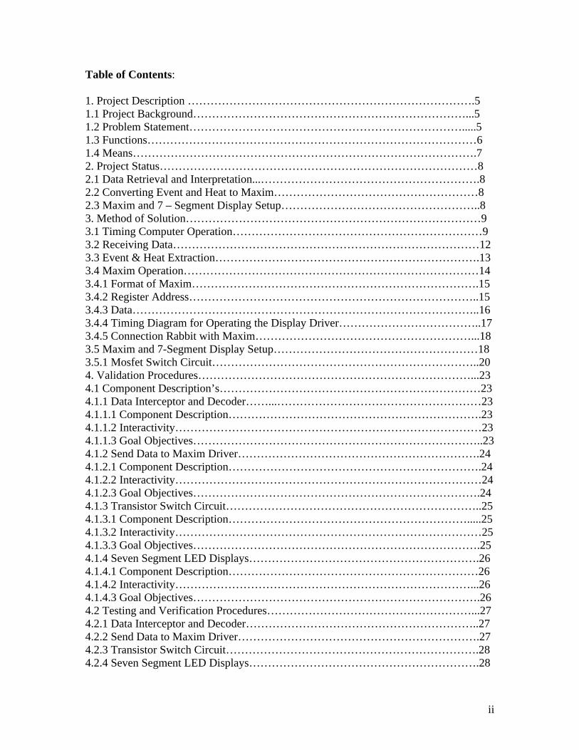
Table of Contents: 1. Project Description ………………………………………………………………….5 1.1 Project Background………………………………………………………………...5 1.2 Problem Statement……………………………………………………………….....5 1.3 Functions……………………………………………………………………………6 1.4 Means……………………………………………………………………………….7 2. Project Status…………………………………………………………………………8 2.1 Data Retrieval and Interpretation...………………………………………………….8 2.2 Converting Event and Heat to Maxim………………………………………………8 2.3 Maxim and 7 – Segment Display Setup……………………………………………..8 3. Method of Solution……………………………………………………………………9 3.1 Timing Computer Operation…………………………………………………………9 3.2 Receiving Data………………………………………………………………………12 3.3 Event & Heat Extraction…………………………………………………………….13 3.4 Maxim Operation……………………………………………………………………14 3.4.1 Format of Maxim………………………………………………………………….15 3.4.2 Register Address…………………………………………………………………..15 3.4.3 Data………………………………………………………………………………..16 3.4.4 Timing Diagram for Operating the Display Driver………………………………..17 3.4.5 Connection Rabbit with Maxim…………………………………………………...18 3.5 Maxim and 7-Segment Display Setup………………………………………………18 3.5.1 Mosfet Switch Circuit……………………………………………………………..20 4. Validation Procedures………………………………………………………………...23 4.1 Component Description’s……………………………………………………………23 4.1.1 Data Interceptor and Decoder……...………………………………………………23 4.1.1.1 Component Description………………………………………………………….23 4.1.1.2 Interactivity………………………………………………………………………23 4.1.1.3 Goal Objectives…………………………………………………………………..23 4.1.2 Send Data to Maxim Driver……………………………………………………….24 4.1.2.1 Component Description………………………………………………………….24 4.1.2.2 Interactivity………………………………………………………………………24 4.1.2.3 Goal Objectives………………………………………………………………….24 4.1.3 Transistor Switch Circuit…………………………………………………………..25 4.1.3.1 Component Description……………………………………………………….....25 4.1.3.2 Interactivity………………………………………………………………………25 4.1.3.3 Goal Objectives………………………………………………………………….25 4.1.4 Seven Segment LED Displays…………………………………………………….26 4.1.4.1 Component Description…………………………………………………………26 4.1.4.2 Interactivity……………………………………………………………………...26 4.1.4.3 Goal Objectives………………………………………………………………….26 4.2 Testing and Verification Procedures………………………………………………...27 4.2.1 Data Interceptor and Decoder……………………………………………………..27 4.2.2 Send Data to Maxim Driver……………………………………………………….27 4.2.3 Transistor Switch Circuit………………………………………………………….28 4.2.4 Seven Segment LED Displays…………………………………………………….28
iii
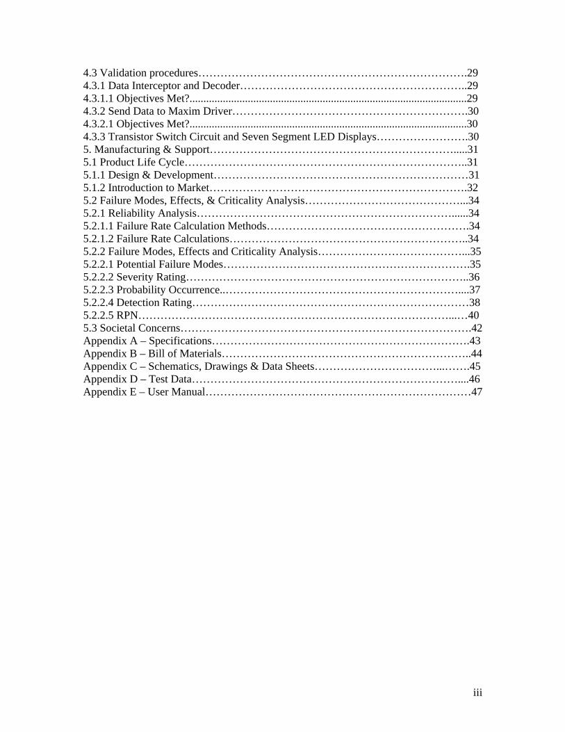
4.3 Validation procedures……………………………………………………………….29 4.3.1 Data Interceptor and Decoder……………………………………………………..29 4.3.1.1 Objectives Met?....................................................................................................29 4.3.2 Send Data to Maxim Driver……………………………………………………….30 4.3.2.1 Objectives Met?....................................................................................................30 4.3.3 Transistor Switch Circuit and Seven Segment LED Displays…………………….30 5. Manufacturing & Support………………………………………………………….....31 5.1 Product Life Cycle…………………………………………………………………..31 5.1.1 Design & Development……………………………………………………………31 5.1.2 Introduction to Market…………………………………………………………….32 5.2 Failure Modes, Effects, & Criticality Analysis……………………………………...34 5.2.1 Reliability Analysis……………………………………………………………......34 5.2.1.1 Failure Rate Calculation Methods……………………………………………….34 5.2.1.2 Failure Rate Calculations………………………………………………………..34 5.2.2 Failure Modes, Effects and Criticality Analysis…………………………………...35 5.2.2.1 Potential Failure Modes………………………………………………………….35 5.2.2.2 Severity Rating…………………………………………………………………..36 5.2.2.3 Probability Occurrence..………………………………………………………....37 5.2.2.4 Detection Rating…………………………………………………………………38 5.2.2.5 RPN…………………………………………………………………………...…40 5.3 Societal Concerns…………………………………………………………………….42 Appendix A – Specifications…………………………………………………………….43 Appendix B – Bill of Materials…………………………………………………………..44 Appendix C – Schematics, Drawings & Data Sheets……………………………...…….45 Appendix D – Test Data………………………………………………………………....46 Appendix E – User Manual………………………………………………………………47
iv
Abstract
The Inland Empire Swimming Committee consists of 19 clubs from parts of Washington and Idaho. All of the clubs share a single scoring system and transport it between meets in a custom-built trailer. The scoring system consists of a scoring computer, which runs a timer, handles incoming time signals, determines placing and sends this information to a scoreboard.
The scoreboard is actually a collection of single, 8.5’ x 14” display boards containing anywhere from 1 to 10 of these individual boards. Because the Inland Empire Swimming Committee has only one of these display boards to use, the useful information is not displayed for a long enough time, namely, the event and heat numbers are displayed very briefly between matches. This results in swimmers and spectators missing their events and not knowing where they are in the meet.
The goal of the swimming scoreboard Senior Design team is to design and build an informational display system to display the current event and heat number for each event and heat. To accomplish this goal, we will employ a microcontroller to receive the data stream coming from the timing computer and to translate the event and heat numbers. We will then send this data on to a display driver that will be running five 7-segment displays. The five displays will present the event number (3 digits) and the heat number (2 digits).

5
1. Project Description 1.1. Project Background
The Inland Empire Swimming Committee consists of 19 clubs from parts of
Washington and Idaho. All of the clubs share a single scoring system and transport it
between meets in a custom-built trailer. The scoring system consists of a scoring
computer, which runs a timer, handles incoming time signals, determines placing and
sends this information to a scoreboard.
1.2. Problem Statement
The scoreboard is actually a collection of single, 8.5’ x 14” display boards
containing anywhere from 1 to 10 of these individual boards. Because the Inland
Empire Swimming Committee has only one of these display boards to use, the useful
information is not displayed for a long enough time, namely, the event and heat numbers
are displayed very briefly between matches. This results in swimmers and spectators
missing their events and not knowing where they are in the meet.
The goal of the swimming scoreboard Senior Design team is to design and build
an informational display system to display the current event and heat number for each
event and heat. To accomplish this goal, we will employ a microcontroller to receive the
data stream coming from the timing computer and to translate the event and heat
numbers. We will then send this data on to a display driver that will be running five 7-
segment displays. The five displays will present the event number (3 digits) and the heat
number (2 digits).
6
1.3. Functions
Our project’s primary objective is to display the event and heat information, with
3 sub-objectives. The first is Data Retrieval and Interpretation, the second is Data
Transmission and the third is Data Display.
1. Data Retrieval and Interpretation:
1.1 Setup a microcontroller’s serial port to receive the data coming from the timing computer.
1.2 Find the channel in the data stream that contain the event and heat
number.
1.3 Interpret the hex values following the channel into the appropriate event and heat number.
2. Data Transmission:
2.1. Convert event and heat number to Maxim display format. Maxim receives 16 bits serial-data which contains register address and actual data .
2.2. Get the clock and chip select working. When chip select is active low, the data begins to be sent. One bit is sent on one clock, so 16 bits data need 16 clocks to be sent.
2.3. Send the setup codes which are the address of control registers. The control registers consist of shutdown mode, decode mode, and scan limit.
2.4. Send actual data which is the event and heat number. The first sent is digit15, the most significant bit.
3. Display the Data:
3.1. Obtain a display driver. We don’t want to program the microcontroller to output the necessary signals to drive the displays.. 3.2. Obtain appropriate displays. We need at least 5” displays, and we will need 5 of them.

7
3.3. Develop a power supply system to drive the displays, display driver, and microcontroller.
1.4. Means
1. Data Retrieval and Interpretation:
1.1 In order to receive the data stream, the microcontroller was setup to receive a serial signal with the same parameters as the timing computer; 9600 BAUD, 8 data bits, 1 stop bit and even parity. Please refer to Appendix A for further timing computer operation information.
1.2 Properly connect the datastream coming from the timing computer to the microcontroller. Since the microcontroller had a female serial
connection, it received serial data on pin 3.
1.3 Only one program for the microcontroller to receive the data, decode the event and heat, and then send the display driver the proper signals. This program has two variables, event_num and heat_num that are updated whenever an incoming event and heat number are detected.
2. Data Transmission:
2.1 The Maxim display driver receives 16 bits serial-data which are labeled D0 – D15. D0-D7 contain the data which is one digit number(0-9), and D8 – D11 contain register address which assign 7 segment LED, and D12 – D15 are “Don’t care” bits. Refer to Appendix B for further information on how the Maxim display driver works. 2.2 Data will be sent to the Maxim using 3 transmission lines. Din (Serial-
Data Input), CS’ (Chip-Select Input), and CLK (Serial-Clock Input).
3. Data Display
3.1 The five 7 segment displays will be connected to the Maxim display driver. 3.2. Voltage regulators will be used to convert the 120V AC input into the appropriate DC voltages for the Maxim chip and 7 segment displays.
8
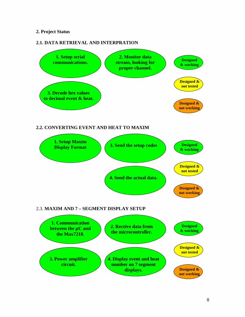
2. Project Status
2.1. DATA RETRIEVAL AND INTERPRATION
2.2. CONVERTING EVENT AND HEAT TO MAXIM
2.3. MAXIM AND 7 – SEGMENT DISPLAY SETUP
1. Communication between the µC and
the Max7218.
2. Receive data from the microcontroller.
3. Power amplifier circuit.
4. Display event and heat number on 7 segment
displays.
Designed & working
Designed & not tested
Designed & not working
1. Setup Maxim Display Format
3. Send the setup codes
4. Send the actual data.
Designed & working
Designed & not tested
Designed & not working
1. Setup serial communications.
2. Monitor data stream, looking for
proper channel.
3. Decode hex values to decimal event & heat.
and heat.
Designed & working
Designed & not tested
Designed & not working
9
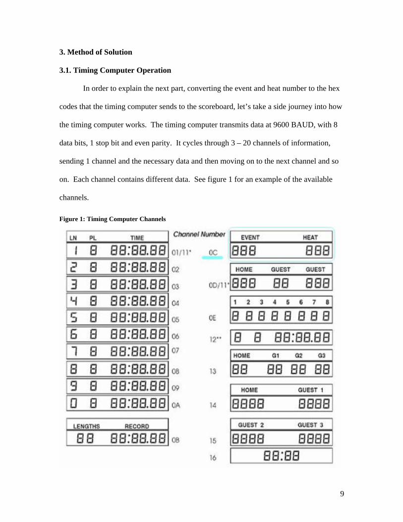
3. Method of Solution 3.1. Timing Computer Operation
In order to explain the next part, converting the event and heat number to the hex
codes that the timing computer sends to the scoreboard, let’s take a side journey into how
the timing computer works. The timing computer transmits data at 9600 BAUD, with 8
data bits, 1 stop bit and even parity. It cycles through 3 – 20 channels of information,
sending 1 channel and the necessary data and then moving on to the next channel and so
on. Each channel contains different data. See figure 1 for an example of the available
channels.
Figure 1: Timing Computer Channels
10
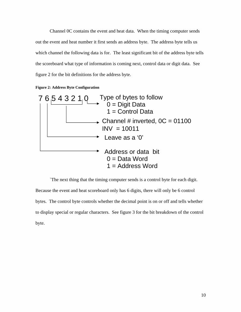
Channel 0C contains the event and heat data. When the timing computer sends
out the event and heat number it first sends an address byte. The address byte tells us
which channel the following data is for. The least significant bit of the address byte tells
the scoreboard what type of information is coming next, control data or digit data. See
figure 2 for the bit definitions for the address byte.
Figure 2: Address Byte Configuration
7 6 5 4 3 2 1 0
Address or data bit0 = Data Word1 = Address Word
Leave as a ‘0’
Channel # inverted, 0C = 01100 INV = 10011
Type of bytes to follow0 = Digit Data1 = Control Data
`The next thing that the timing computer sends is a control byte for each digit.
Because the event and heat scoreboard only has 6 digits, there will only be 6 control
bytes. The control byte controls whether the decimal point is on or off and tells whether
to display special or regular characters. See figure 3 for the bit breakdown of the control
byte.
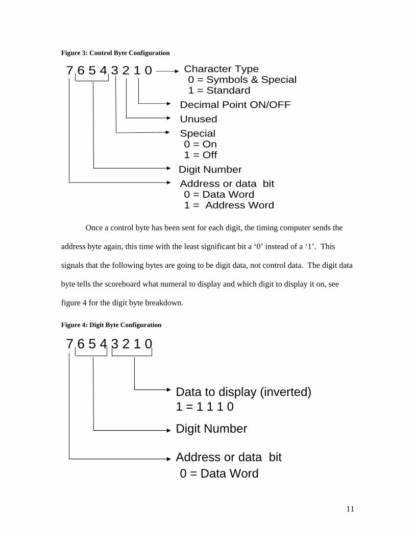
11
Figure 3: Control Byte Configuration
7 6 5 4 3 2 1 0
Address or data bit0 = Data Word1 = Address Word
Digit Number
Special
Character Type0 = Symbols & Special1 = Standard
0 = On1 = Off
UnusedDecimal Point ON/OFF
Once a control byte has been sent for each digit, the timing computer sends the
address byte again, this time with the least significant bit a ‘0’ instead of a ‘1’. This
signals that the following bytes are going to be digit data, not control data. The digit data
byte tells the scoreboard what numeral to display and which digit to display it on, see
figure 4 for the digit byte breakdown.
Figure 4: Digit Byte Configuration
7 6 5 4 3 2 1 0
Address or data bit0 = Data Word
Digit Number
Data to display (inverted) 1 = 1 1 1 0
12
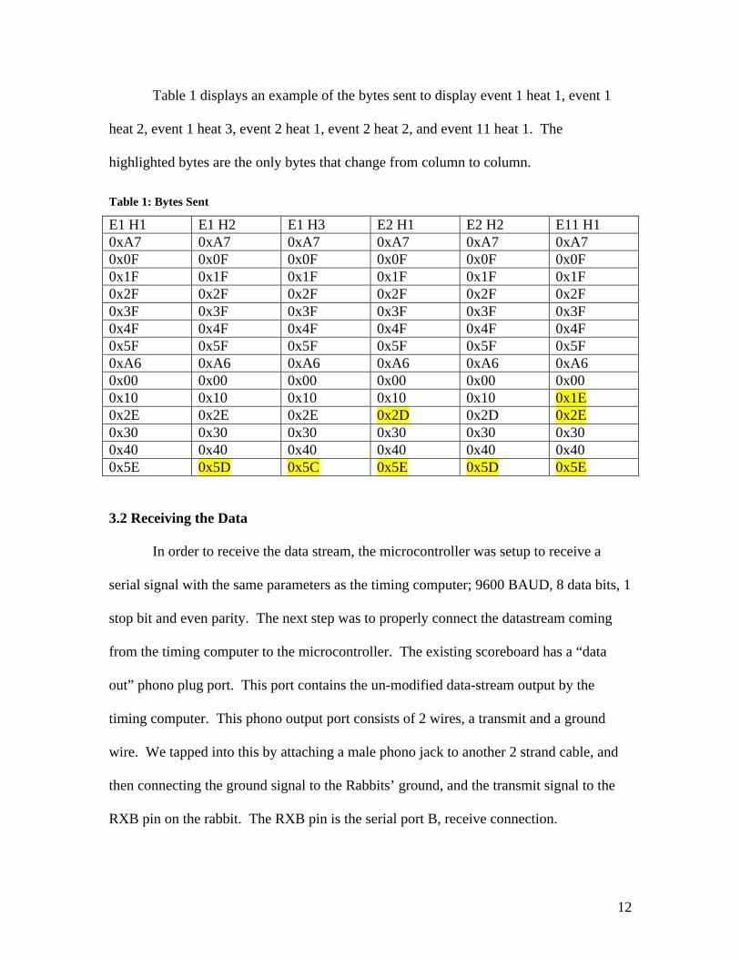
Table 1 displays an example of the bytes sent to display event 1 heat 1, event 1
heat 2, event 1 heat 3, event 2 heat 1, event 2 heat 2, and event 11 heat 1. The
highlighted bytes are the only bytes that change from column to column.
Table 1: Bytes Sent
E1 H1 E1 H2 E1 H3 E2 H1 E2 H2 E11 H1 0xA7 0xA7 0xA7 0xA7 0xA7 0xA7 0x0F 0x0F 0x0F 0x0F 0x0F 0x0F 0x1F 0x1F 0x1F 0x1F 0x1F 0x1F 0x2F 0x2F 0x2F 0x2F 0x2F 0x2F 0x3F 0x3F 0x3F 0x3F 0x3F 0x3F 0x4F 0x4F 0x4F 0x4F 0x4F 0x4F 0x5F 0x5F 0x5F 0x5F 0x5F 0x5F 0xA6 0xA6 0xA6 0xA6 0xA6 0xA6 0x00 0x00 0x00 0x00 0x00 0x00 0x10 0x10 0x10 0x10 0x10 0x1E 0x2E 0x2E 0x2E 0x2D 0x2D 0x2E 0x30 0x30 0x30 0x30 0x30 0x30 0x40 0x40 0x40 0x40 0x40 0x40 0x5E 0x5D 0x5C 0x5E 0x5D 0x5E
3.2 Receiving the Data
In order to receive the data stream, the microcontroller was setup to receive a
serial signal with the same parameters as the timing computer; 9600 BAUD, 8 data bits, 1
stop bit and even parity. The next step was to properly connect the datastream coming
from the timing computer to the microcontroller. The existing scoreboard has a “data
out” phono plug port. This port contains the un-modified data-stream output by the
timing computer. This phono output port consists of 2 wires, a transmit and a ground
wire. We tapped into this by attaching a male phono jack to another 2 strand cable, and
then connecting the ground signal to the Rabbits’ ground, and the transmit signal to the
RXB pin on the rabbit. The RXB pin is the serial port B, receive connection.

13
Every time a byte is received it triggers an interrupt and gets stored in a received
buffer. When a byte is put into the received buffer, it is checked to see if is equal to
0xA6, which means channel 0C, digit data to follow. If it is, then the next 8 bytes
coming from the timing computer are captured into a generic array to hold them while the
decoding operations are taking place.
If a value greater than 0x7F is received before 8 bytes have been captured after
0xA6, the channel was interrupted and this value is the new channel. Any stored bytes
are discarded, and the Rabbit will wait for the next 0xA6 to come by. 0x7F was chosen
as the cutoff value because of the way the timing computer sends data. At the very most,
the timing computer will never send data for more than 8 digits. Since the digit number
is contained in the most significant digit of the hex number, anything over 0x7F is greater
than the number of digits supported, and therefore must be a new channel number.
3.3 Event & Heat Extraction
When 8 bytes are received after 0xA6, and none of them are greater than 0x7F,
the event and heat extraction function is called. The extraction function goes through the
array containing the 8 digit data bytes and performs comparisons on them. If the byte is
less than 16, we know it is for digit 0, if it is between 16 and 32 we know it is for digit 1,
if it’s between 32 and 48 it is for digit 2 and so on. A series of if statements are used to
make these comparisons and determine which digit the byte contains data for.. Once
inside the proper ‘if’ statement, the byte is sent to the compute_numeral function that
returns the appropriate decimal value.
The compute_numeral function first mod’s the byte with 16 to get the remainder
and get rid of the digit number part. The remainder is then the inverted binary equivalent
14
of the decimal numeral. A series of switch/case statements quickly turns this inverted
binary number into the proper decimal equivalent. This is then returned to the parent
function which multiplies it by 100, 10, or 1 (depending on the digit number) and adds it
to the appropriate temporary heat or event number. We know which one to multiply by,
because the if statements pick out which digit that the byte is for. Only the first 3 bytes
and the last 3 bytes are used. The first 3 bytes contain the event number, and the last 3
bytes contain the heat number.
3.4 Maxim Operation
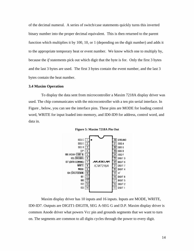
To display the data sent from microcontroller a Maxim 7218A display driver was
used. The chip communicates with the microcontroller with a ten pin serial interface. In
Figure , below, you can see the interface pins. These pins are MODE for loading control
word, WRITE for input loaded into memory, and ID0-ID9 for address, control word, and
data in.
Figure 5: Maxim 7218A Pin Out
Maxim display driver has 10 inputs and 16 inputs. Inputs are MODE, WRITE,
ID0-ID7. Outputs are DIGIT1-DIGIT8, SEG A-SEG G and D.P. Maxim display driver is
common Anode driver what powers Vcc pin and grounds segments that we want to turn
on. The segments are common to all digits cycles through the power to every digit.
15
3.4.1 Format of Maxim
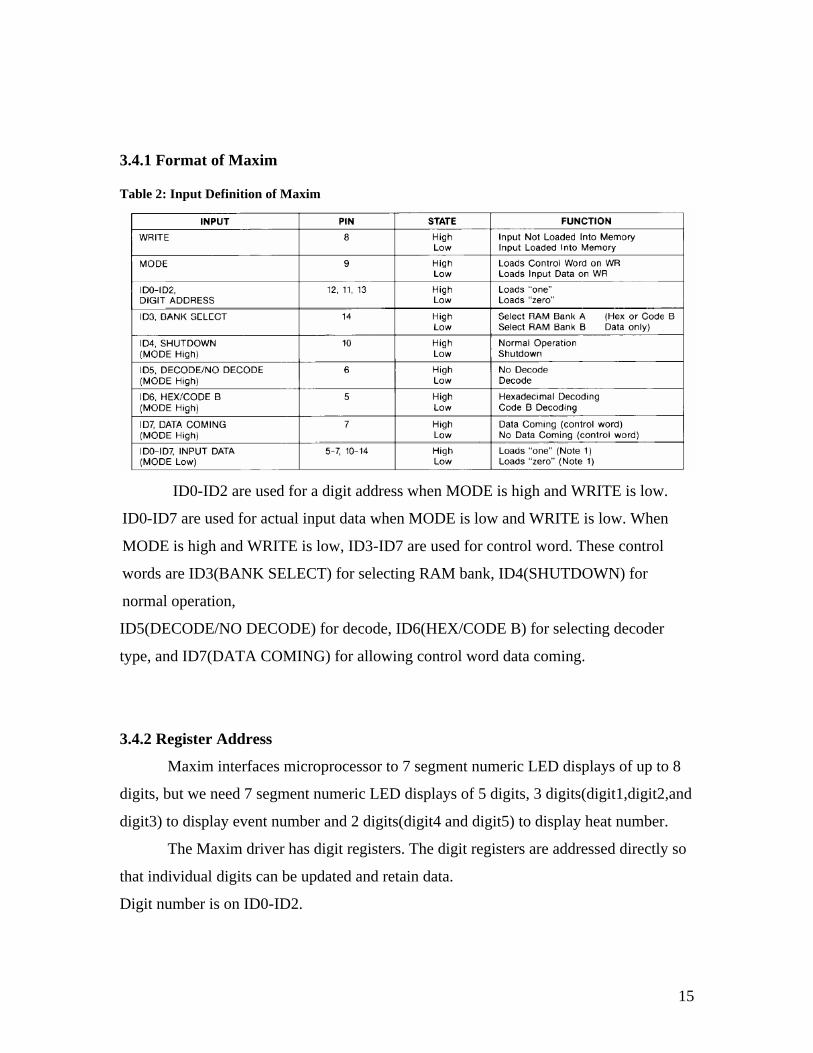
Table 2: Input Definition of Maxim
ID0-ID2 are used for a digit address when MODE is high and WRITE is low.
ID0-ID7 are used for actual input data when MODE is low and WRITE is low. When
MODE is high and WRITE is low, ID3-ID7 are used for control word. These control
words are ID3(BANK SELECT) for selecting RAM bank, ID4(SHUTDOWN) for
normal operation,
ID5(DECODE/NO DECODE) for decode, ID6(HEX/CODE B) for selecting decoder
type, and ID7(DATA COMING) for allowing control word data coming.
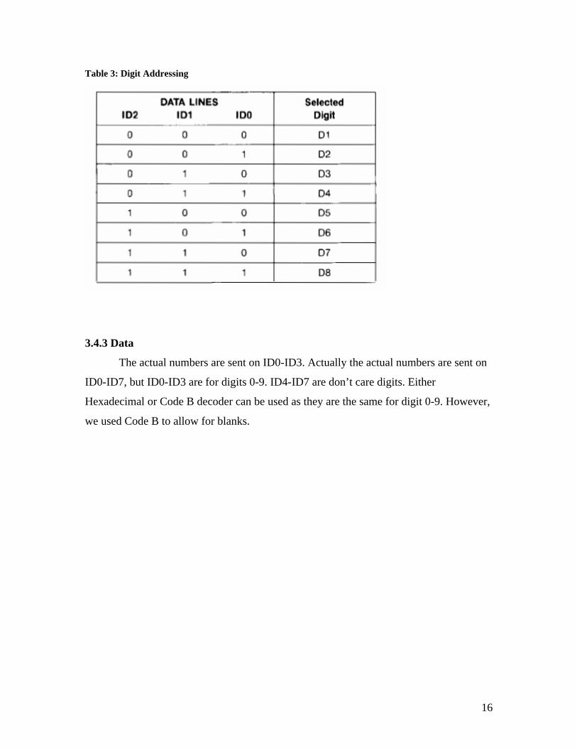
3.4.2 Register Address
Maxim interfaces microprocessor to 7 segment numeric LED displays of up to 8
digits, but we need 7 segment numeric LED displays of 5 digits, 3 digits(digit1,digit2,and
digit3) to display event number and 2 digits(digit4 and digit5) to display heat number.
The Maxim driver has digit registers. The digit registers are addressed directly so
that individual digits can be updated and retain data.
Digit number is on ID0-ID2.
16
Table 3: Digit Addressing
3.4.3 Data
The actual numbers are sent on ID0-ID3. Actually the actual numbers are sent on
ID0-ID7, but ID0-ID3 are for digits 0-9. ID4-ID7 are don’t care digits. Either
Hexadecimal or Code B decoder can be used as they are the same for digit 0-9. However,
we used Code B to allow for blanks.
17
Table 4: Display Font
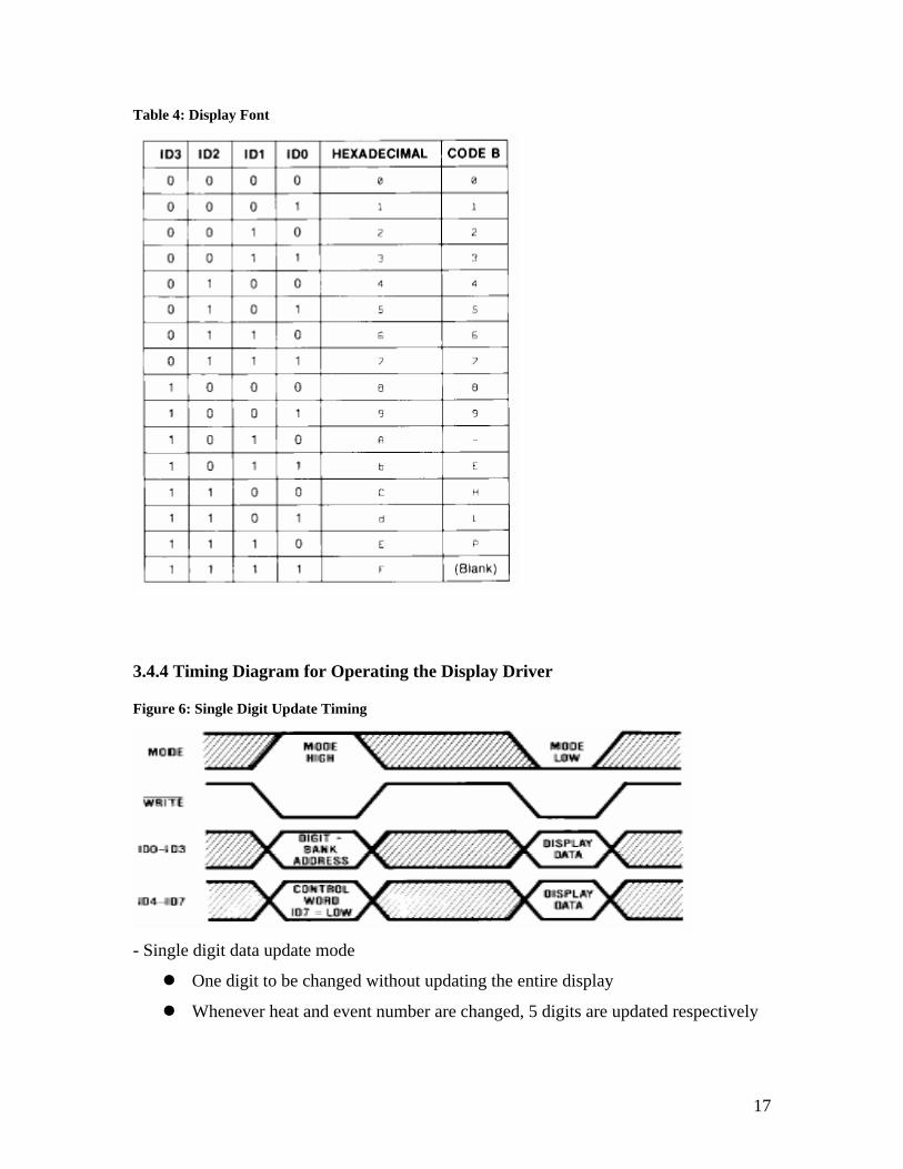
3.4.4 Timing Diagram for Operating the Display Driver
Figure 6: Single Digit Update Timing
- Single digit data update mode
l One digit to be changed without updating the entire display
l Whenever heat and event number are changed, 5 digits are updated respectively
18
- First, the control register is updated with MODE high, Data coming low, and the
address of the digit to be updated. Second, the actual data is transferred from ID0-ID7
into the selected digit’s RAM location with MODE low.
3.4.5 Connection Rabbit with Maxim
- Rabbit microprocessor needs 10 input pins. We used 2 from port C, 3 from port D, and
5 from port E.
ü MODE = pin9 on display driver, PD3 on rabbit
ü WRITE = pin8 on display driver, PD4 on rabbit
ü ID0 = pin12 on display driver, PD5 on rabbit
ü ID1 = pin11 on display driver, PE0 on rabbit
ü ID2 = pin13 on display driver, PE1 on rabbit
ü ID3 = pin14 on display driver, PC0 on rabbit
ü ID4 = pin10 on display driver, PE2 on rabbit
ü ID5 = pin6 on display driver, PC2 on rabbit
ü ID6 = pin5 on display driver, PE4 on rabbit
ID7 = pin7 on display driver, PE5 on rab
3.5 Maxim and 7 – Segment Display Setup
To display the data sent from the microcontroller a Maxim ICM7218A display
driver was used. The chip communicates with the microcontroller with a ten pin serial
interface. In Figure 5, above, you can see the interface pins. These pins are ID0-ID3, ID4
for shutdown mode, ID5 for decode, ID6 for HEX A/CodeB, ID7 for data coming, write,
and mode.
The V+ pin is the 5V positive supply voltage. DIG1-DIG8 pins were to control
each of the digits. The SEGA-SEGG pins were used to connect to each of the 7 segments.
These connections would source current to the display segments. The chip was able to
control each of the digits by constantly refreshing the digits. Once a digit is written it will
hold that value until it changed by a new data stream. The refresh rate of the chip is so
19
fast that the human eye can’t detect it therefore it looks as if it is always on, instead of
blinking.
The 7 segment displays are common anode, which means that all the anodes are
connected together and sending a low signal to each of the cathodes controls each of the
segments. Each of the digits segment is made of 10 LED’s in series. The height of each
digit is 5 inches and the height of each segment is 2.5 inches. The maximum ratings for
the 7 segment displays are as follows: The forward voltage per LED is 2 V at 20mA.
Since the forward voltage per LED was 2.0 volts, we needed to use 24 volts at 15 mA for
each digit to reach its maximum brightness. Since the Maxim driver digit output was 5
volts, the 24-volt source was switched using a MOSFET circuit that was controlled by the
Maxim driver output signals.
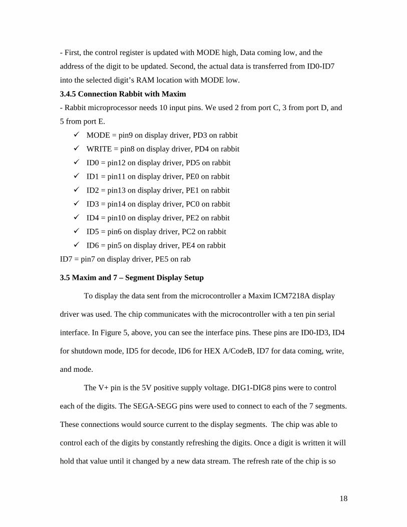
Figure 7: Maxim Driver Output Flow Chart and Truth Table

20
The way that the Maxim display driver controls the digits and segment is shown
in figure 6. According to the truth table the only way that a segment will turn on is when
the (+) digit output of the driver is high and when the (–) segment output is low. The
MOSFET switch circuit will not respond to any other case.
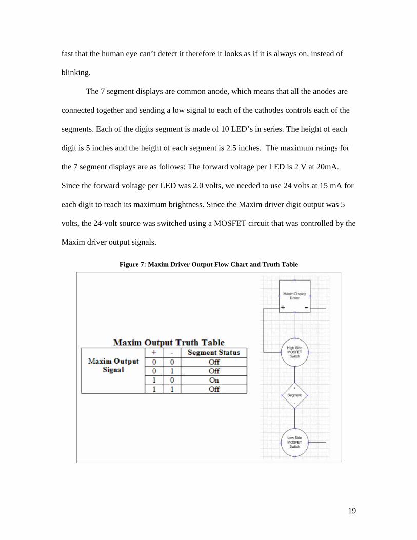
3.5.1 MOSFET Switch Circuit
In order to switch sufficient power to the digits a MOSFET switch circuit was
designed to control the voltage and current levels. The switch circuit was made of 2
2N7000 NMOS transistors, a SPPB08PO6P PMOS transistor, a logic inverter and 2 one-
quarter watt resistors. This switch has a high side voltage of 24 volts, which is controlled
by the Maxim driver digit and segment outputs. The following figure (Figure 8) shows
the circuit diagram of the switch.
21
Figure 8: Mosfet Switch Schematic
The complete circuit contains five high side switches, for each of the digits; and
seven low side switch, for each of the segments. When the MOSFET switch was initially
designed, a 5 k ohm resistor was used for the resistance between the +24 volts and the
PMOS gate. The only problem with this was that a large resistor along with the internal
capacitance was creating a large (RC) time constant. This large time constant would lead
to a ghosting effect on the digits as the Maxim driver cycled through the digits. The
following figure (Figure 9) shows the voltage across the 5k resistor.
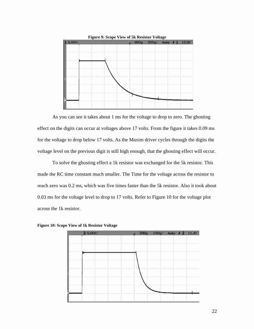
22
Figure 9: Scope View of 5k Resistor Voltage
As you can see it takes about 1 ms for the voltage to drop to zero. The ghosting
effect on the digits can occur at voltages above 17 volts. From the figure it takes 0.09 ms
for the voltage to drop below 17 volts. As the Maxim driver cycles through the digits the
voltage level on the previous digit is still high enough, that the ghosting effect will occur.
To solve the ghosting effect a 1k resistor was exchanged for the 5k resistor. This
made the RC time constant much smaller. The Time for the voltage across the resistor to
reach zero was 0.2 ms, which was five times faster than the 5k resistor. Also it took about
0.03 ms for the voltage level to drop to 17 volts. Refer to Figure 10 for the voltage plot
across the 1k resistor.
Figure 10: Scope View of 1k Resistor Voltage
23
4. Validation Procedures
4.1. Component Description’s
4.1.1 Data Interceptor and Decoder
4.1.1.1 Component Description
The data interceptor and decoder is the component that will intercept the data
coming from the timing computer and then extract the event and heat numbers from the
data stream. This component consists of a connection to the data stream coming from the
timing computer as well as software for the Rabbit microprocessor.
4.1.1.2 Interactivity
The data interceptor and decoder connects directly to the data stream from the
timing computer via a serial connection that is physically plugged into the existing
scoreboard. The existing scoreboard has a data out terminal that routs incoming data
from the timing computer directly through to the next scoreboard in line. Our data
interceptor will connect at this point. After extracting the appropriate event and heat
number from this data stream it will send these numbers to the next component in line,
the Send Data to Display Driver component.
4.1.1.3 Goal Objectives
This component will achieve the objectives of intercepting the data stream
coming from the timing computer and extracting the event and heat information from that
data.

24
4.1.2 Send Data to Maxim Driver.
4.1.2.1 Component Description.
The Send Data to Maxim Driver is the component that will send the data from the
Rabbit microprocessor to Maxim driver. The Rabbit processor receives the event and heat
number from the Interpreter and Decoder component. This Send Data to Maxim Driver
component converts event and heat number to Maxim diver format and sends 10 bit serial
data which contain register address and actual data.
4.1.2.2 Interactivity
The Maxim display driver interfaces the Rabbit microprocessor to a 5 digit 7
segment display. The Rabbit microprocessor sends converted data which contain control
registers, register address, and actual data to Maxim driver. Converted data is for single
digit update mode which allows one digit to be changed without updating the entire
display. The each event and heat number is sent to maxim driver whenever event and heat
number is updated from timing computer. In single digit update mode, first the control
register is updated with MODE high, WRITE low, DATA COMING low, the desired
data format, and the address of the digit to be updated on data lines. A second write to the
Maxim driver, this time with MODE low, transfers the actual data into selected digit's
RAM location. Whenever event and heat number is updated, single digit update occur
five times for 3 digit event number and 2 digit heat number. After sending data, Maxim
driver will drive 5 7-segment displays.
4.1.2.3 Goal Objectives
This components objective is to send data which contain control registers, register
address, and actual data to Maxim driver. To send data to Maxim driver, the data from

25
timing computer should be converted to Maxim display format.
4.1.3 Transistor Switch Circuit
4.1.3.1. Component Description.
The transistor switch circuit handles the task of taking the 5-volt output control
signal from the Maxim display driver and switches the 24-volt power supply to the 7-
segment displays. This is necessary because the output of the Maxim is only 5 volts,
which is much less than the voltage that the displays run at. This component consists of a
NPN bipolar transistor and a 24-volt power supply.
4.1.3.2 Interactivity
The common anode of the 7-segment display is connected to the positive 24-volt
supply and each segment is connected to the collector of each transistor. The emitter is
connected to the negative of the voltage supply. The control voltage from the Maxim
display driver is connected across the base and emitter. When the control signal from the
display driver is sent to the transistor it send current through the base emitter and the
transistor acts as a switch to connect the 24 volts to the 7-segment display.
4.1.3.3 Goal Objectives
This components objective is to act as a switch to supply the necessary voltage to
the 7-segment displays using the low voltage control signal from the display driver.
26
4.1.4 Seven Segment LED Displays.
4.1.4.1 Component Description.
The 7-segment displays are used to display the event and heat numbers that are
generated from the timing computer. The displays are made up of 7-segments and each
segment consists of 10 LED’s that are in series. Due to the internal circuitry of the
LED’s each display needs 18 volts to bring the display to its brightest state. This supply
voltage is high because the voltage drop across each diode is .7 volts and each LED
needs about 1 volt to bring it to its brightest state.
4.1.4.2 Interactivity
Each display digit is connected to its respective transistor switch circuit
depending on which digit it is. There are three digits used to display the event and two
digits to display the heat. The common anode of each digit is connected to the positive
voltage from the power supply and each segment is connected to the collector of each
transistor. The circuit is then completed when the display driver sends the control signal
to its respective digit, therefore displaying the correct event and heat numbers for the
meet.
4.1.4.3 Goal Objectives
This components objective is to display the event and heat numbers that are
generated from the timing computer. These displays must be bright enough to be read
from about 100 feet so all the viewers can see them.

27
4.2 Testing and Verification Procedures
4.2.1 Data Interceptor and Decoder
To test the data interceptor and decoder component, the timing computer was
going to be used to set up a practice swim event and change event and heat numbers. The
data stream would be connected to the component and the data interceptor and decoder
would work its magic. Unfortunately, the timing computer that was going to be used for
testing broke, and with the main timing computer being used for swim meets, this was no
longer a viable option.
Luckily, we were able to obtain sample data from the timing computer. With this
sample data, a timing computer simulator was set up on another microcontroller and this
would output data in the format of the timing computer. This data stream would be used
to test the data interceptor and decoder.
To test the data interceptor and decoder component, the sample data stream
coming from the timing computer simulator will be connected to the input of the data
interceptor and decoder. The sample data stream will contain known values for the event
and heat. Intermixed with these hex values will be hex values for other channels and
random information. Also, the event and heat data will start to be sent, and then be
interrupted by another channel, in order to see if the data interceptor and decoder can
recover the proper event and heat numbers.
4.2.2 Send Data to Maxim Driver
To test the Send Data to Maxim Driver, The Rabbit microcontroller will be
connected to the data interceptor and decoder and receive the current event and heat
numbers. The Rabbit microcontroller also will be connected to the Maxim
28
microcontroller. The Rabbit microcontroller needs 10 I/O ports for output. The Maxim
driver will receive the data from 10 I/O ports Rabbit microcontroller output. In order to
see if the Maxim driver receives the proper event and heat numbers, the Maxim display
driver will be connected to 5 digit 7-segment displays and 7-segment displays will
display the data in proper numbers and positions.
4.2.3 Transistor Switch Circuit
To test the transistor switch circuit a series of voltages and current were ran
through the collector and the base. These voltages were similar to the ones that are
supplied by the display system. To test, an LED was connected from the supply voltage
to the collector and a simulated control signal was sent to the base emitter. When the
control signal was sent through the base the LED on the collector turned on, which means
the circuit works as planned.
After the circuit performed to its expectations, it was tested for its maximum
ratings. The maximum ratings that were used for the testing were way above the circuit’s
normal ratings. Therefore there is a huge margin or error if the circuit becomes unstable
for some reason.
4.2.4 Seven Segment LED Displays.
The 7-segment displays were tested by running the rated current through each
segment of each digit. This showed that the digits were not defective. The digits then
were tested in the transistor switch circuit. As the control signal from the display driver
was sent to the digit it would light up each of the corresponding digits. This test showed
that the transistor switch circuit could in fact be used to run the digits from the low
29
voltage control signals from the display driver. After this was done there was not much
else used to test the digits because a failure test was out of the question.
4.3. Validation Procedures
4.3.1 Data Interceptor and Decoder
In order to validate the results achieved from testing the data interceptor and
decoder, the output of the function (the extracted event and heat numbers) will be
compared with the event and heat numbers that were input. If this component is
functioning properly, an incoming event and heat number should produce an identical
outgoing event and heat number.
4.3.1.1 Objectives Met?
The objectives for the data interceptor and decoder component were:
-intercepting the data stream coming from the timing computer.
-extracting the event and heat information from that data.
The data interceptor and decoder met the objective of intercepting the data stream
coming from the decoder. The data stream is input to the microcontroller via a serial
connection at 9600 BAUD and even parity.
The data interceptor and decoder met the objective of extracting the event and
heat information from the data stream. Even when the event and heat were interrupted,
the component waited until they were fully sent again before updating the internal event
and heat numbers.

30
4.3.2 Send Data to Maxim Driver
In order to validate the results achieved from testing the Send Data to Maxim
Driver, the output of the component (the current event and heat numbers) will be
displayed on 7-segment displays in proper numbers and positions.
4.3.2.1. Objectives Met?
The objectives for the Send Data to Maxim Driver were:
- converting Maxim display format
- sending data to Maxim driver.
The Send Data to Maxim Driver met the objective of converting Maxim display
format. The control registers, register address and actual data for Maxim display driver
are set.
The Send Data to Maxim Driver met the objective of sending data to Maxim
driver. The Rabbit microcontroller needs 10 I/O ports for output. The Maxim driver will
receive the data from 10 I/O ports Rabbit microcontroller output.
4.3.3 Transistor Switch Circuit and Seven Segment LED Displays.
In order to validate the results achieved from transistor switch circuit and the 7-
segment displays, the digits must be displaying the correct event and heat numbers. Also
to validate the transistor circuit the display must be bright enough to be seen from about
200 feet away.

31
5. Manufacturing & Support
5.1 Product Life Cycle
The Swim Team Scoreboard Project has identified six stages in the product
lifecycle of the event and heat display board:
1. Design & Development 2. Introduction 3. Growth 4. Maturity 5. Decline 6. Death
For each of these stages, we will answer
• Who are the customers or users? • What support will they need? • What needs, concerns, problems will they face? • What issues affect support costs? • How can product revenue be maximized? • What effect do design choices have on the PLC?
As a brief refresher, the event and heat display board will be attached to the existing
scoreboard, and will rely on data coming from the timing computer in order to find the
current event and heat numbers, and then display them continuously throughout the meet.
5.1.1 Design & Development
In the design and development stage, the event and heat scoreboard progressed
from an idea, to a plan, to a functioning prototype, and from there to a useable product.
There are no customers for this stage (besides the sponsor, who won’t be using the
product during the design and development stage), but the users are none other than
ourselves. When we test each part of the finished product we will be using it, as well as
the testing of the finished product to ensure functionality.
32
Since we are the design and construction team, the support we need will come in
the form of advice and suggestions from our sponsor’s and advisors. We also will utilize
the manufacturer of the timing computer for information on the output of their system, so
that we will be able to integrate our system with theirs appropriately.
As far as needs, concerns, and problems that we will encounter, they will all be
design and manufacture related. Several big hurdles have presented themselves over the
course of this project. The first was interpreting the data stream that emanates from the
timing computer, finding out all the dirty little details about how it works, the format of
the data, where the pertinent information was, etc. The next big hurdle was setting up a
communications link between the outside world and our system, as well as the subparts
of our system.
The support costs are entirely the cost of the equipment and supplies needed at
this stage. Because we do not have a production-ready model, we have no incoming
revenue, so it can’t be maximized at this stage. One of the requirements laid out by the
customer was to minimize the overall cost of this system. We have worked this in to the
design, by going with a microcontroller that offered a one-time high cost for licensing
and software, but the actual microcontroller product is fairly cheap if bought in quantity.
The rest of the products that we decided to use are easily obtainable to allow for future
replacement of worn-out or broken parts. We have also endeavored to minimize the
number of individual parts in our system to maximize the total lifetime of our product.
5.1.2 Introduction to Market
In the introduction to market phase, the primary customer will be our sponsor, the
Inland Empire Swimming Committee. After an initial trial and exposure at a swim meet,
33
the customers will be any of the swimming teams within the Inland Empire Swimming
division, as well as any other teams with representatives present to view the operation of
our system. The customer base will slowly grow as word spreads from team to team,
although this will never be a high volume product, it could conceivably be sold in the
thousands, eventually.
The initial customers should not need a lot of support. Another design
consideration was to make this product as user friendly as possible. The theory of
operation is to be able to plug in the power and the data line coming from the existing
scoreboard and it will handle itself from there. Sufficient testing will have been
performed on the system in the design phase to ensure full functionality and error free
operation. In the unlikely event that something does go wrong, there are only 2 support
options. Either a part needs to be replaced, or the code needs to be tweaked.
As far as needs, concerns, or problems that the initial customers will face, the
product will be used in a hostile environment, e.g. high humidity, lots of transportation,
possible rough handling, possible immersment, etc. Any of these situations could present
a problem for our customer. If the event and heat display does break as a result of one or
more of the above conditions, the likely culprit will be physical hardware. The software
will survive, which is where most of the development cost would normally go to in this
type of product.
The support costs at this stage will likely come from the failure of any hardware
that would need to be replaced. Although unlikely, it is possible that some small costs
could be incurred by a need for further tweaking of the code, if the unit does not perform
as expected, or if something slipped by in testing.
34
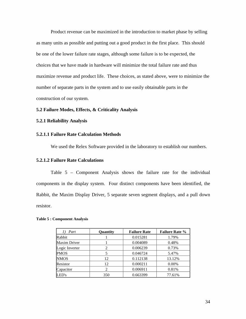
Product revenue can be maximized in the introduction to market phase by selling
as many units as possible and putting out a good product in the first place. This should
be one of the lower failure rate stages, although some failure is to be expected, the
choices that we have made in hardware will minimize the total failure rate and thus
maximize revenue and product life. These choices, as stated above, were to minimize the
number of separate parts in the system and to use easily obtainable parts in the
construction of our system.
5.2 Failure Modes, Effects, & Criticality Analysis
5.2.1 Reliability Analysis
5.2.1.1 Failure Rate Calculation Methods
We used the Relex Software provided in the laboratory to establish our numbers.
5.2.1.2 Failure Rate Calculations
Table 5 – Component Analysis shows the failure rate for the individual
components in the display system. Four distinct components have been identified, the
Rabbit, the Maxim Display Driver, 5 separate seven segment displays, and a pull down
resistor.
Table 5 : Component Analysis
1) Part Quantity Failure Rate Failure Rate % Rabbit 1 0.015281 1.79% Maxim Driver 1 0.004089 0.48% Logic Inverter 2 0.006239 0.73% PMOS 5 0.046724 5.47% NMOS 12 0.112138 13.12% Resistor 12 0.000211 0.00% Capacitor 2 0.006911 0.81% LED's 350 0.663399 77.61%
35
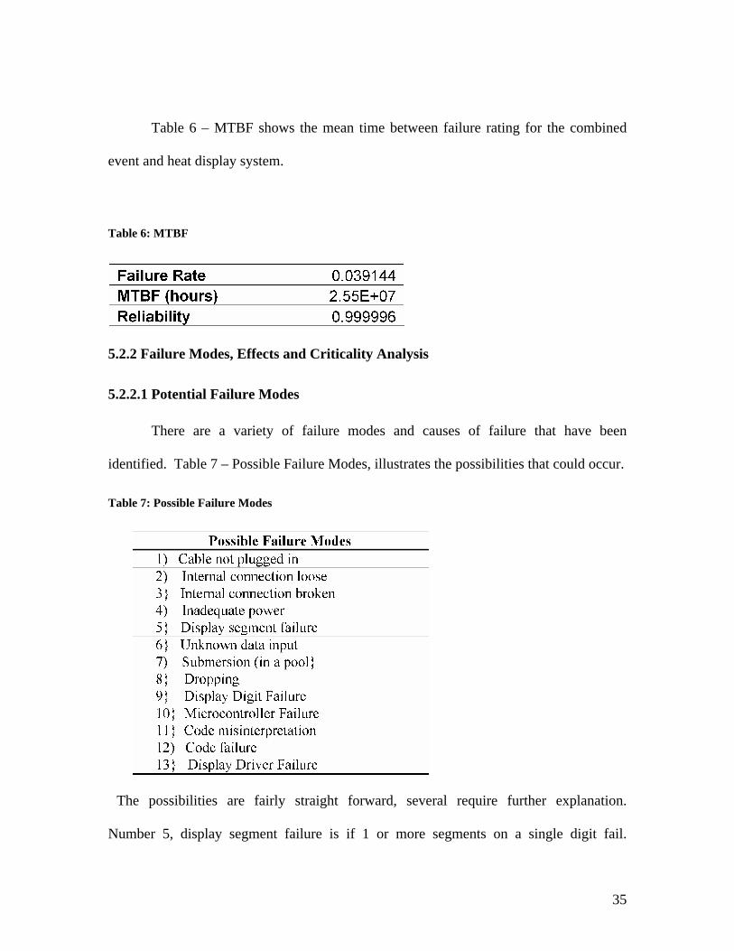
Table 6 – MTBF shows the mean time between failure rating for the combined
event and heat display system.
Table 6: MTBF
5.2.2 Failure Modes, Effects and Criticality Analysis
5.2.2.1 Potential Failure Modes
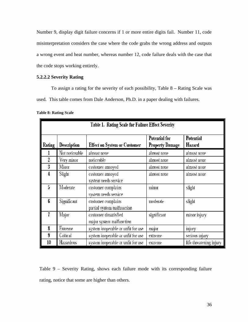
There are a variety of failure modes and causes of failure that have been
identified. Table 7 – Possible Failure Modes, illustrates the possibilities that could occur.
Table 7: Possible Failure Modes
The possibilities are fairly straight forward, several require further explanation.
Number 5, display segment failure is if 1 or more segments on a single digit fail.
36
Number 9, display digit failure concerns if 1 or more entire digits fail. Number 11, code
misinterpretation considers the case where the code grabs the wrong address and outputs
a wrong event and heat number, whereas number 12, code failure deals with the case that
the code stops working entirely.
5.2.2.2 Severity Rating
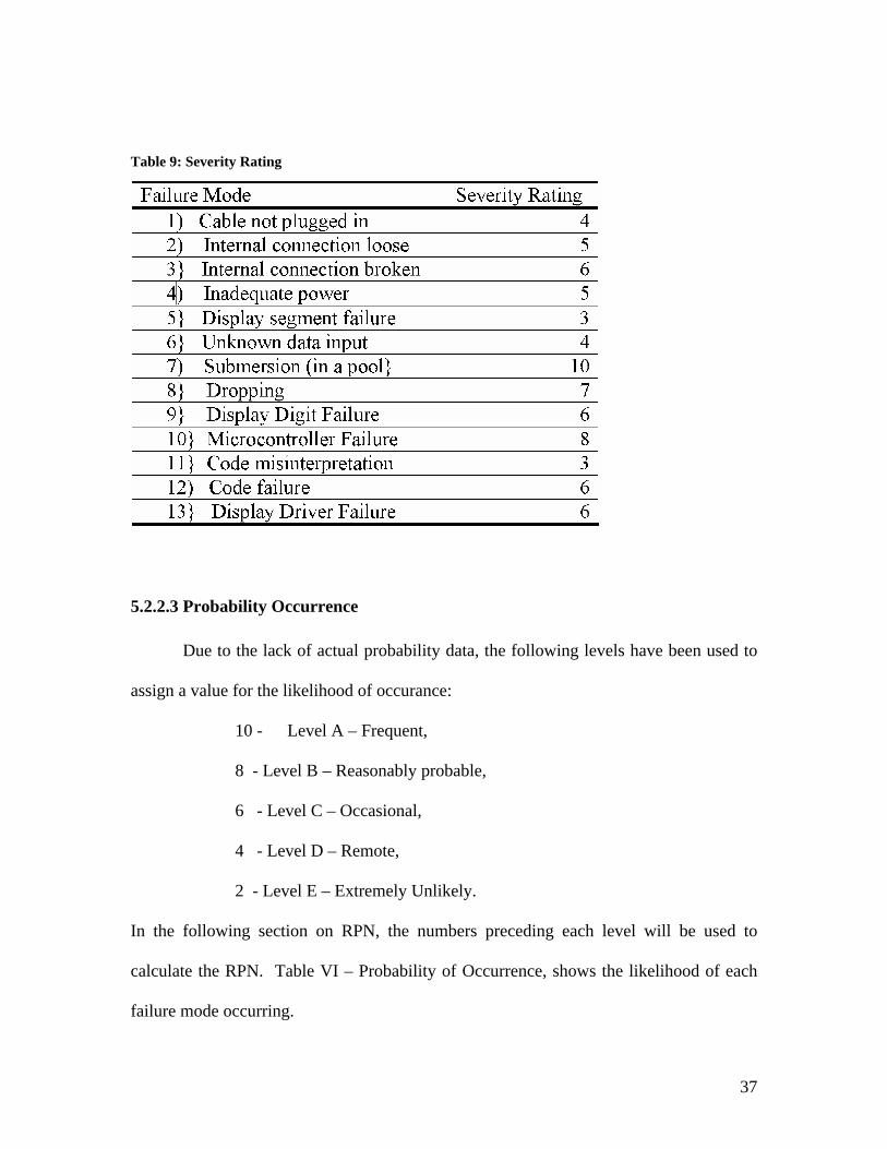
To assign a rating for the severity of each possibility, Table 8 – Rating Scale was
used. This table comes from Dale Anderson, Ph.D. in a paper dealing with failures.
Table 8: Rating Scale
Table 9 – Severity Rating, shows each failure mode with its corresponding failure
rating, notice that some are higher than others.
37
Table 9: Severity Rating
5.2.2.3 Probability Occurrence
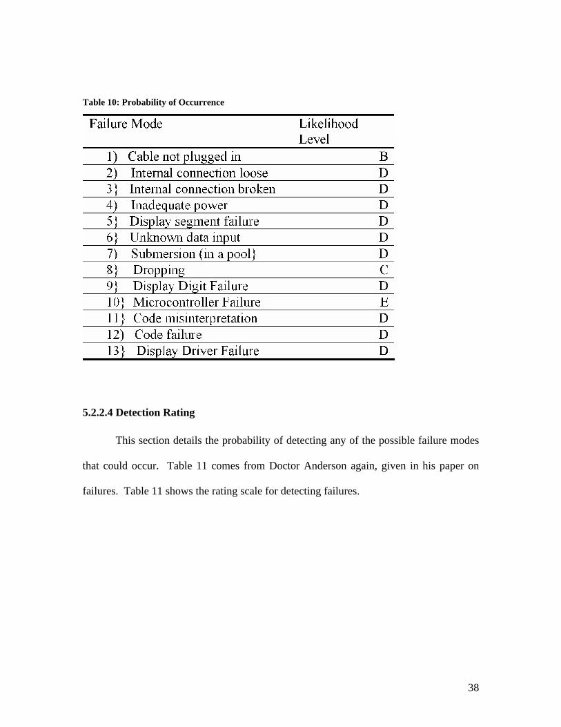
Due to the lack of actual probability data, the following levels have been used to
assign a value for the likelihood of occurance:
10 - Level A – Frequent,
8 - Level B – Reasonably probable,
6 - Level C – Occasional,
4 - Level D – Remote,
2 - Level E – Extremely Unlikely.
In the following section on RPN, the numbers preceding each level will be used to
calculate the RPN. Table VI – Probability of Occurrence, shows the likelihood of each
failure mode occurring.
38
Table 10: Probability of Occurrence
5.2.2.4 Detection Rating
This section details the probability of detecting any of the possible failure modes
that could occur. Table 11 comes from Doctor Anderson again, given in his paper on
failures. Table 11 shows the rating scale for detecting failures.
39
Table 11: Detection Rating
Table 12 – Failure Detection illustrates the possibilities of detecting each of the failure
modes.

40
Table 12: Detection Likelihood
5.2.2.5 RPN
The final part of this Analysis is the Risk Priority Number (RPN). The RPN
illustrates the failure modes that present the most risk to the system. Table IX – RPN
Calculations shows the failure modes in descending order with the greatest RPN shown
first. The RPN is calculated by multiplying the failure severity rating by the probability
of occurrence, by the probability of detection. Remember for the probability of
occurrence, a modified ranking has been used, as described above.
41
Table 13: RPN - Calculations
Table X – RPN, shows the final RPN values according to rank.
42
Table 14: RPN
5.3 Societal Concerns
The only concerns are that the 24V power supply will supply enough current (5A)
that it could be a hazard if misused. Also, if the display board is submerged or dropped
in a pool, electrocution, while unlikely, could possibly result.
In order to make the display board more rugged, a printed circuit board should be
developed. This will result in a decrease in the number of required wires for the entire
system. Also, the wires that still remain can be either encased in round cable wrap or
replaced with some type of wire strip, and the ends could even be sauderd on.
43
Appendix A – Specifications
Inputs:
- RS232 Input via ¼” phono plug - 9600 Baud - Even Parity - 8 data bits - 1 stop bit
- 120V AC input
Outputs:
None
Physical:
- Maxim 7218A Common Anode Display Driver - Rabbit RCM2200 - 5 – 5” 7-Segment Displays - 5 – PMOS SPP08P06P TO-220 Package - 12 – NMOS 2N7000 TO-92 Package - SN7404 Logic Inverter - 24V Power Supply
Electrical:
- Rabbit Microcontroller & Proto-Board – 12V DC - Maxim Display Driver – 5V DC - Logic Inverter – 5V DC - Mosfet High Side Switch – 24V DC - Mosfet Control Signal – 0-5V DC
44
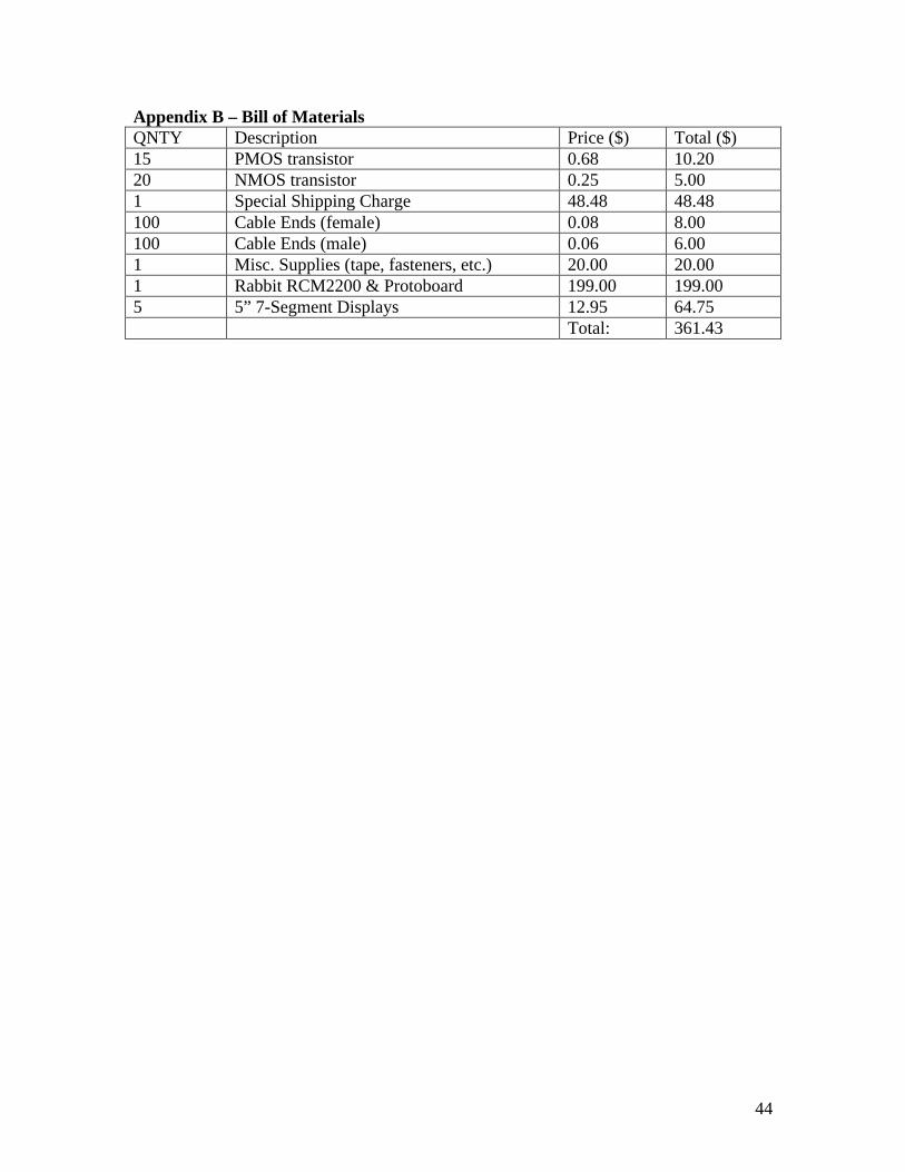
Appendix B – Bill of Materials QNTY Description Price ($) Total ($) 15 PMOS transistor 0.68 10.20 20 NMOS transistor 0.25 5.00 1 Special Shipping Charge 48.48 48.48 100 Cable Ends (female) 0.08 8.00 100 Cable Ends (male) 0.06 6.00 1 Misc. Supplies (tape, fasteners, etc.) 20.00 20.00 1 Rabbit RCM2200 & Protoboard 199.00 199.00 5 5” 7-Segment Displays 12.95 64.75 Total: 361.43

45
Appendix C – Schematics, Drawings & Data Sheets

46
Appendix D – Test Data

47
Appendix E – Users Manual
I. Introduction
The purpose of this manual is to provide a basic overview and understanding of
the event and heat display board. This manual will cover the installation and initial setup
of the event and heat display board, as well as how to use it. Finally, and perhaps the
most important aspect covered will be the troubleshooting section.
The event and heat display board is a simple device with only two inputs. The
first is a phono plug for receiving data, and the second is a standard power plug that will
work on any 120V AC standard wall outlet. The purpose of the display board is to
continuously show the current event and heat numbers of a swim meet.
II. Installation
The installation process of the event and heat display board is remarkably simple.
Since this display board is meant to be somewhat transportable, this installation topic will
refer to setting up the display board at every new meet.
The first step in installing the event and heat display board is to connect the grey
phono plug coming out of the device into either the Colorado System’s Timing Computer
directly, or into the data output port of an existing scoreboard. The second step is to plug
the power cord coming out of the device into either an extension cord coming from a wall
outlet or directly into a wall outlet. Finally, ensure that the event and heat display board
is in a secure, sturdy location.
III. Initial Setup
48
Like the Installation section, this Initial Setup section will reference the process
that occurs whenever the display device is brought to a new meet. This means that the
display board will need to be installed and setup multiple times.
After the installation procedures have been followed, and the timing computer is
up and running, the display board is ready to go and should not require any more
attention, other than to adjust the angle or location.
IV. Using the System
This display board will work with the Colorado Timing Systems System 4 or 5
timing computer, anything earlier or later has not been tested and is not guaranteed to
work. The communications speed of the timing computer must be set at 9600 BAUD. If
this is the case, the display board is ready to go and should be displaying the event and
heat number that is on the timing computer.
The digits and digit driver are common anode type. This means that to turn on a
segment, the digit’s power pin is applied with 18V, and the segment(s) that we want on
are grounded. The other segments are not grounded. As a result, each digit has 1 power
wire going into it, along with 7 segment wires. The single power wire is unique to each
digit, but all of the digits share the same segment wires.
The grey phono wire coming into the device is the data carrier. It contains only 2
separate wires. The black wire with the green tape around it is ground and can be
connected to any available ground pin on the Rabbit (refer to figure 1). The other one is
red and can be connected to only the RXB pin on the Rabbit. Again, refer to figure 1 for
the location of these pins.

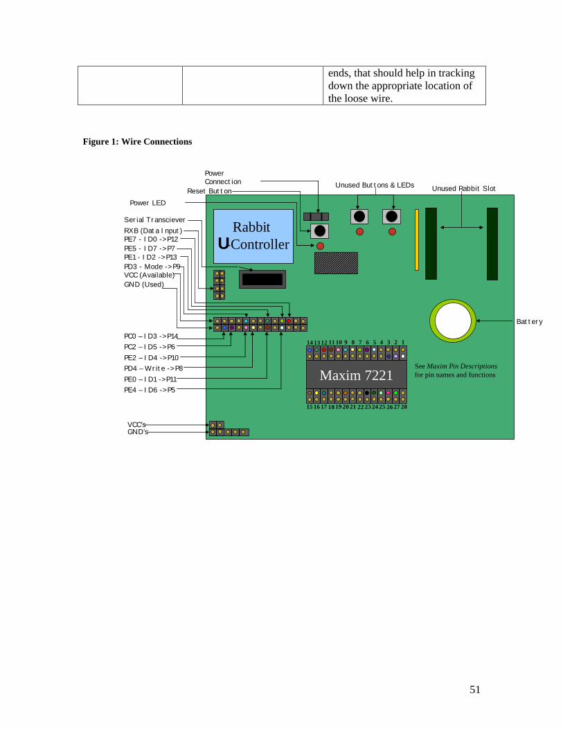
49
The Rabbit microcontroller needs to communicate with the Maxim display driver,
so there are 10 short wires going from one part of the green board to another. These
connections are somewhat colorcoded and the appropriate connections can be found by
referring to Figure 1. The Maxim display driver then sends 5 digit outputs (the power
signal) and 7 segment outputs to the amplifier circuits. The outputs of these amplifier
circuits go directly to the digit’s, either a power signal or a segment signal. Refer to
Figure XX for the appropriate connections (color coded).
V. Troubleshooting
This troubleshooting section will identify the main and most likely problems that
can occur, as well as the multiple causes and individual solutions for each problem.
Following is a list of problems covered in this section:
1. All digits are blank 2. The board only displays a ‘0’ for the event and a ‘0’ for the heat 3. 1 or more digits dos’t turn on at all 4. Certain segments of the digits don’t turn on 5. A wire came loose
The table below, table I shows the problems as well as their various causes and solutions.
Table 15: Troubleshooting
Problem Cause Solution The power cord is not plugged in.
1. Make sure that the power cord coming from the display board is plugged in to a wall outlet.
The internal outlet strip is turned off.
Reach in and flip the orange switch away from “Off”
1 or both of the internal power cords are unplugged from the outlet strip
Carefully plug them back in and ensure that the outlet strip is turned on
The small red & white striped wires coming from the 24V power supply are not connected to the circuits
Referring to Figure 1, carefully insert the loose power cable back into the appropriate place on the circuit board.
All digits are blank
All of the digit power wires Referring to Figure 1, carefully
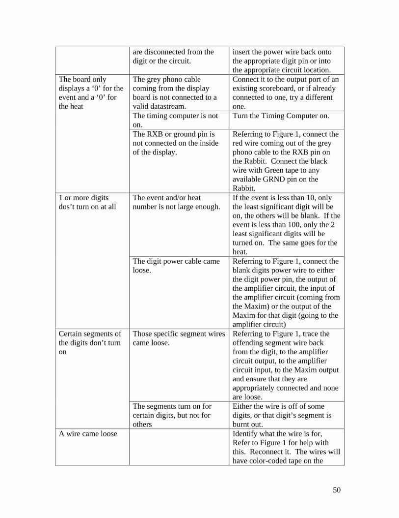
50
are disconnected from the digit or the circuit.
insert the power wire back onto the appropriate digit pin or into the appropriate circuit location.
The grey phono cable coming from the display board is not connected to a valid datastream.
Connect it to the output port of an existing scoreboard, or if already connected to one, try a different one.
The timing computer is not on.
Turn the Timing Computer on.
The board only displays a ‘0’ for the event and a ‘0’ for the heat
The RXB or ground pin is not connected on the inside of the display.
Referring to Figure 1, connect the red wire coming out of the grey phono cable to the RXB pin on the Rabbit. Connect the black wire with Green tape to any available GRND pin on the Rabbit.
The event and/or heat number is not large enough.
If the event is less than 10, only the least significant digit will be on, the others will be blank. If the event is less than 100, only the 2 least significant digits will be turned on. The same goes for the heat.
1 or more digits dos’t turn on at all
The digit power cable came loose.
Referring to Figure 1, connect the blank digits power wire to either the digit power pin, the output of the amplifier circuit, the input of the amplifier circuit (coming from the Maxim) or the output of the Maxim for that digit (going to the amplifier circuit)
Those specific segment wires came loose.
Referring to Figure 1, trace the offending segment wire back from the digit, to the amplifier circuit output, to the amplifier circuit input, to the Maxim output and ensure that they are appropriately connected and none are loose.
Certain segments of the digits don’t turn on
The segments turn on for certain digits, but not for others
Either the wire is off of some digits, or that digit’s segment is burnt out.
A wire came loose
Identify what the wire is for, Refer to Figure 1 for help with this. Reconnect it. The wires will have color-coded tape on the
51
ends, that should help in tracking down the appropriate location of the loose wire.
Figure 1: Wire Connections
Rabbit U-Controller
Power Connection
Reset ButtonPower LED
Unused Buttons & LEDs Unused Rabbit Slot
Battery
Serial TranscieverRXB (Data Input)
PD3 - Mode -> P9
PE7 - ID0 -> P12PE5 - ID7 -> P7PE1 - ID2 -> P13
VCC (Available)GND (Used)
PC0 – ID3 -> P14PC2 – ID5 -> P6PE2 – ID4 -> P10PD4 – Write -> P8PE0 – ID1 -> P11PE4 – ID6 -> P5
Maxim 7221
1234567891011121314
18171615 22212019 26252423 2827
See Maxim Pin Descriptionsfor pin names and functions
VCC’sGND’s