Influence of deposition parameters on the structure and ... · Influence of deposition parameters...
28
Manufacturing Nanostructures 293 11 Influence of deposition parameters on the structure and properties of nitride coatings A.D. Pogrebnjak 1* , N.A. Azarenkov 2 , V.M. Beresnev 2 , S.V. Litovchenko 2 1 Sumy State University, 2, Rymsky Korsakov Str., 40007 Sumy, Ukraine 2 Kharkiv National University, 21, Svobody Sq., 4, 61022 Kharkiv, Ukraine Outline: Introduction………………………………………………………………………………………………………………………………… 294 Methods……………………………………………………………………………………………………………………………………… 294 Conclusions…………………………………………………………………………………………………………………………………. 316 References………………………………………………………………………………………………………………………………….. 317
Transcript of Influence of deposition parameters on the structure and ... · Influence of deposition parameters...

Manufacturing Nanostructures 293 293
11 Influence of deposition parameters on the structure and properties of nitride coatings A.D. Pogrebnjak
1*, N.A. Azarenkov
2, V.M. Beresnev
2, S.V. Litovchenko
2
1Sumy State University, 2, Rymsky Korsakov Str., 40007 Sumy, Ukraine 2Kharkiv National University, 21, Svobody Sq., 4, 61022 Kharkiv, Ukraine
Outline: Introduction………………………………………………………………………………………………………………………………… 294 Methods……………………………………………………………………………………………………………………………………… 294 Conclusions…………………………………………………………………………………………………………………………………. 316 References………………………………………………………………………………………………………………………………….. 317

Manufacturing Nanostructures 294 294
Introduction
High-entropy alloys (HEAs) – are multicomponent alloys containing five or more principal elements, mixed in equiatomic ratios [1]. The main difference between conventional multi-component alloys and HEAs is that HEAs don’t have a dominant principle element; and this concept is a breakthrough in the field of alloys development [2-10]. Phase composition investigations of high-entropy alloys evidence, that predominantly only one solid-solution phase with fcc and/or bcc lattice, or amorphous phase is formed in HEAs. Formation of the various phases is not observed. Such structural stability promotes improves the physical and mechanical characteristics of HEAs. Various nitrides ([11-19]) and carbides [20] based on high-entropy were investigated. High mechanical hardness and Young modulus, high durability and corrosion resistance, thermal stability make high-entropy alloys one of the promising and interesting materials in science.
Methods High-entropy alloy TiZrHfVNb was obtained using vacuum-arc melting in anatmosphere of high-purity argon Ar. Melting was performed using nonconsumable tungsten electrode and a copper water-cooled hearth. To homogenize the alloy, the ingots were remelted six to seven times. Nitrides of high-entropy alloys (TiZrHfVNb)N were obtained using cathodic-vacuum-arc-vapor-deposition in a Bulat-6 setup. [21] The following deposition parameters were used: substrate voltage bias (Ub) varied from -40 V to -200 V, the arc current did not exceed 85 A, working gas pressure (N2) in the chamber varied from 0.03 Pa to 0.7 Pa. The deposition conditions employed for all of samples, are presented in Table 11.1. TABLE 11.1 Deposition parameters and lattice parameters for multicomponent coatings (TiZrHfVNb)N
№ Ub, V P, Pa Concentration, % Lattice
parameter, а, nm
N Ti V Zr Nb Hf
504* -200 710-1
– 44 5 30 5 14 0.4420
505 -110 510-1
49,15 16,63 5,91 8,17 8,88 11,26 0,4405
506 -100 210-1
49,05 22,92 5,04 6,84 7,47 8,68 0,4380
507 -50 510-1
51,13 25,31 4,72 5,70 6,31 6,84 0,4362
508* -100 110-1
– 57 5 18 5 13 0.4380
509 -100 310-2
44,70 25,31 4,57 7,60 7,99 9,83 0,4376
510 -50 210-1
49,11 19,67 5,65 7,68 8,24 9,64 0,4395
512 -200 810-2
46,65 17,03 2,79 12,01 12,54 8,99 0,4435
513 -40 810-2
– 34,66 8,88 19,53 23,16 13,76 0,3371
514 -200 210-1
47,69 16,41 1,93 13,34 13,90 6,72 0,4435
515 -200 310-2
36,05 20,13 2,28 17,12 17,50 6,93 0,4433
523 -230 2.310-1
43,44 17,80 1,45 16,39 16,99 3,92 0,4408 * – concentration of composing elements determined by RBS analysis
Manufacturing Nanostructures 295 295
Thermal annealing was conducted under the temperature 600°С under a residual pressure of 100 Pa for 30 min in air using a furnace Vacutherm-Ceram VT 1200.X-ray diffraction (XRD) was used to investigate the structure and phase composition of nitride high-entropy coatings (TiZrHfVNb)N.
X-ray strain measurement method and technique of multiple inclined shooting with α-sin2
dependencies were used to determine level of residual stresses in the coatings, elastic properties of materials (Poisson's ratio), and crystal lattice period in the unstressed state. The phase composition and structural studies were performed on the X-ray diffractometer DRON-3M and Rigaku RINT-2500, MDG Japan, in the filtered radiation of Cu-Ka using in the secondary beam graphite monochromator. The diffraction spectra were surveyed in the point-by-point scanning mode with a step 2Θ = 0.05–0.1. X-ray diffraction was employed using a grazing incidence beam, in Cr emission, at angle 3. To study the stress-strain state of the coatings, X-ray strain measurements (“α-sin
2φ” method) and its modifications
commonly applied to the coatings with strong axial texture [21–25] was used. Transmission electron microscopy was used for investigation of the structure and phase composition of high-entropy alloys nitrides (TiZrHfVNb)N after thermal treatment. Transmission electron microscope used was JEOL 2100F in the light-field mode, and in diffraction mode, with accelerating voltage 200 kV and 250 kV. Elemental composition and elemental distribution in the depth of the coating were obtained using Rutherford backscattering spectrometry (RBS) method with He
+ ions of 1.7 MeV the scattering angle
was =170 with a normal fall of probing ions to the surface of coated samples. The energy resolution of detector was 16 keV. A dose of helium ions was 5 Ci. To interpret the RBS spectra and element profiles over the coatings depth, standard software was used [26].The RBS method can determine the presence major elements in the coating but it is not suitable for concentration with satisfactory accuracy. Therefore, energy-dispersive spectroscopy (EDS) method was used. Scanning electron microscope (SEM with EDS) JEOL – 7000F (Japan) was also used. The SEM images of coatings’ surface, its cross-section, and elemental distribution in the coatings and cross-section in elemental contrast were obtained. A positron annihilation spectroscopy (PAS) (Halle, Germany) was used for analysis of vacancy type defects. Using slow positron microbeam was obtained by positron annihilation energy spectra, to enable calculation of important characteristic of material, the S-parameter of Doppler broadening of an annihilation peak depending on the energy of the incident positron beam (30 keV), i.e. on the depth of the analysis [27]. Proton microbeam (μ-PIXE) was employed for elemental analysis. The initial energy of an electrostatic accelerator IAP (Sumy) was 1.4 MeV with the beam size of 0.4 μm (the charge was 3x10
−10 C/pixel, the
raster was 50x50, and the step size was 0.5 μm) *28+.Elements maps of Ti, Zr, Hf, V, Nb distribution before (as deposited) and after annealing up to 873 K were obrained. Mechanical properties such as microhardness and Young modulus were measured using Micro Durometer produced by CSM (Switzerland); load changed discrete from 500 mN to 1.5 N. Vickers hardness was measured using Micro Durometer DM8-B under loads of 0.05 kg and 0.1kg. Tribological properties (friction coefficient, wear rate) of nitride coatings were investigated on the automated friction machine “Tribometer”, GSM Instruments in air atmosphere by “ball-disk” scheme at 293 K. The ball with a diameter of 6 mm was made of sintered certificated material-Al2O3. The coatings were deposited on steel (45 HRC = 55) discs with a diameter of 50 mm and a thickness of 5 mm. The load was 3.0 N, sliding velocity 10 cm/s. The microscopic investigation of wear grooves, and elemental composition were investigated.
Manufacturing Nanostructures 296 296
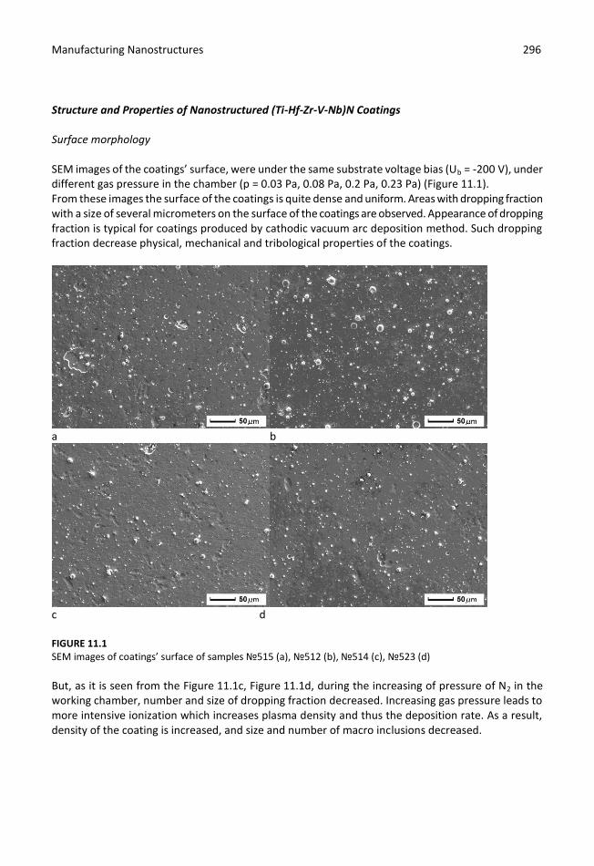
Structure and Properties of Nanostructured (Ti-Hf-Zr-V-Nb)N Coatings Surface morphology SEM images of the coatings’ surface, were under the same substrate voltage bias (Ub = -200 V), under different gas pressure in the chamber (p = 0.03 Pa, 0.08 Pa, 0.2 Pa, 0.23 Pa) (Figure 11.1). From these images the surface of the coatings is quite dense and uniform. Areas with dropping fraction with a size of several micrometers on the surface of the coatings are observed. Appearance of dropping fraction is typical for coatings produced by cathodic vacuum arc deposition method. Such dropping fraction decrease physical, mechanical and tribological properties of the coatings.
а b
c d FIGURE 11.1 SEM images of coatings’ surface of samples №515 (a), №512 (b), №514 (c), №523 (d)
But, as it is seen from the Figure 11.1c, Figure 11.1d, during the increasing of pressure of N2 in the working chamber, number and size of dropping fraction decreased. Increasing gas pressure leads to more intensive ionization which increases plasma density and thus the deposition rate. As a result, density of the coating is increased, and size and number of macro inclusions decreased.
Manufacturing Nanostructures 297 297
Elements and phase structure
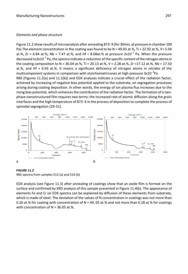
Figure 11.2 show results of microanalysis after annealing 873∘K (for 30min, at pressure in chamber 100 Pa).The element concentration in the coating was found to be N = 49.05 at.%, Ti = 22.92 at.%, V= 5.04
at.%, Zr = 6.84 at.%, Nb = 7.47 at.%, and Hf = 8.68at.% at pressure 2x10⁻² Pa. When the pressure
decreased to3x10−2 Pa, the spectra indicate a reduction of the specific content of the nitrogen atoms in
the coating composition to N = 36.04 at.%, Ti = 20.13 at.%, V = 2.28 at.%, Zr =17.12 at.%, Nb = 17.50 at.%, and Hf = 6.93 at.%. It means a significant deficiency of nitrogen atoms in nitrides of the
multicomponent systems in comparison with stoichiometricones at high pressure 3x10⁻²Pa.
RBS (Figures 11.2(a) and 11.2(b)) and EDX analyses indicate a crucial effect of the radiation factor, achieved by increasing of negative bias potential applied to the substrate, on segregation processes arising during coating deposition. In other words, the energy of ion plasma flux increases due to the rising bias potential, which enhances the contribution of the radiation factor. The formation of a two-phase nanostructured film requires two terms: the increased rate of atomic diffusion along the grain
interfaces and the high temperature of 873∘K in the process of deposition to complete the process of spinodal segregation [29-31].
a b FIGURE 11.2 RBS spectra from samples 512 (a) and 510 (b)
EDX analysis (see Figure 11.3) after annealing of coatings show that an oxide film is formed on the surface and confirmed by XRD analysis of this sample presented in Figure 11.4(b). The appearance of elements Fe and Cr on EDX spectra can be explained by diffusion of these elements from substrate, which is made of steel. The deviation of the values of N concentration in coatings was not more than 0.26 at.% for coating with concentration of N = 49, 05 at.% and not more than 0.18 at.% for coatings with concentration of N = 36.05 at.%.

Manufacturing Nanostructures 298 298
FIGURE 11.3 Microanalysis of coatings, N, Ti, V, Zr, Nb after annealing 873K (for 30 min, at pressure in chamber 100 Pa)
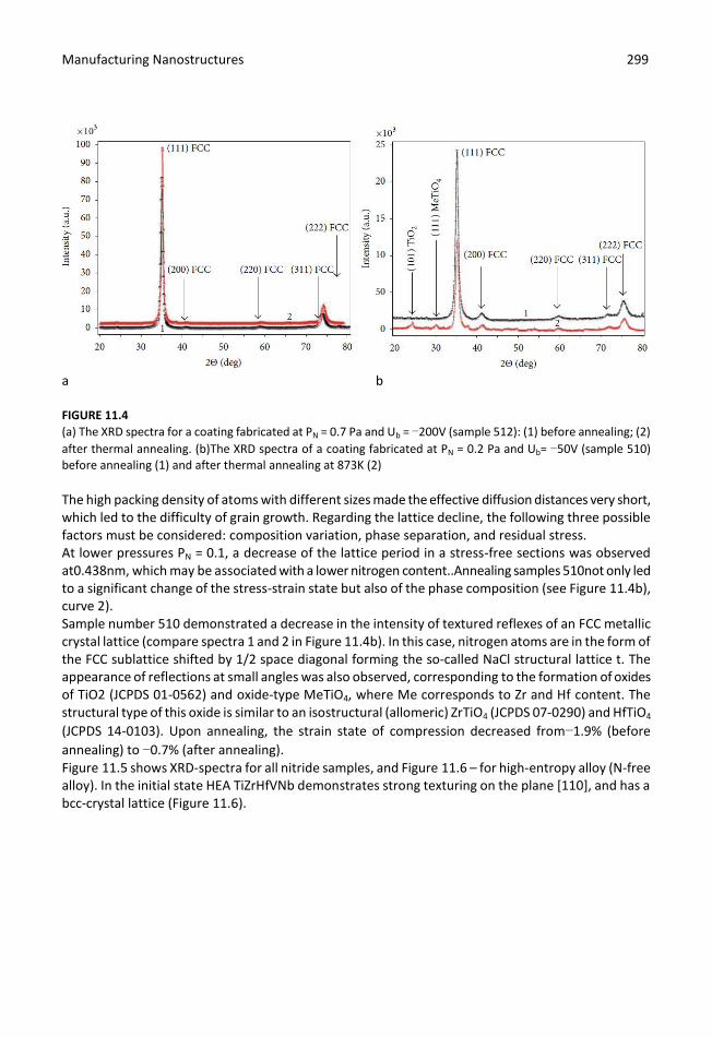
X-ray diffraction for the sample 512 shows the formation of a strong texture with the (111) axis, which is perpendicular to the plane of growth (Figure 11.4). X-ray strain measurements indicate that the samples 512are characterized by the highest value of a lattice period in a stress-free cross-section (a = 0.442 nm). It correlates well with the results of elemental analysis, according to which the highest concentration of nitrogen is observed when the working pressures are high.
An appearance of biaxial texture with (111) and (110) axes at Ubias = −200V resulted in formation of coatings with the highest hardness reaching 58 to 60 GPa and very uniform and smooth surfaces [32-35]. Thermal annealing did not significantly change the structure-phase state of the coatings (Figure 11.4a). However, it reduces a little the deformed state of compression from the strain ratio of 2.76% in initial state (as-deposited state) to 2.59% after annealing. There was only a slight increase from56nm to 68nm of crystal size and a decrease from 0.4424 Ǻ to 0.4386 Ǻ of lattice constant, with annealing temperature from RT to 873 K. The small change in structure and grain size at high temperature annealing may be attributed to the small driving force due to the low grain boundary energy and low kinetics from the sluggish diffusion. The grain boundary energy comes from the energy difference between the state of grain boundaries and that inside the grains. The large lattice distortion effect because of large atomic size difference (the atomic size Ti,1.462 Ǻ; V, 1.316 Ǻ; Zr, 1.603 Ǻ; Hf, 1.578 Ǻ;Nb, 3.301) can markedly raise the overall free energy of crystalline structure. The actual grain boundary energy was lowered significantly leading to very small driving force for coarsening. A detailed mechanism has been proposed by Huang and Yeh [12] for (AlCrNbSiTiV)N coatings.
Manufacturing Nanostructures 299 299
a b FIGURE 11.4
(a) The XRD spectra for a coating fabricated at PN = 0.7 Pa and Ub = −200V (sample 512): (1) before annealing; (2)
after thermal annealing. (b)The XRD spectra of a coating fabricated at PN = 0.2 Pa and Ub= −50V (sample 510) before annealing (1) and after thermal annealing at 873K (2)
The high packing density of atoms with different sizes made the effective diffusion distances very short, which led to the difficulty of grain growth. Regarding the lattice decline, the following three possible factors must be considered: composition variation, phase separation, and residual stress. At lower pressures PN = 0.1, a decrease of the lattice period in a stress-free sections was observed at0.438nm, which may be associated with a lower nitrogen content..Annealing samples 510not only led to a significant change of the stress-strain state but also of the phase composition (see Figure 11.4b), curve 2). Sample number 510 demonstrated a decrease in the intensity of textured reflexes of an FCC metallic crystal lattice (compare spectra 1 and 2 in Figure 11.4b). In this case, nitrogen atoms are in the form of the FCC sublattice shifted by 1/2 space diagonal forming the so-called NaCl structural lattice t. The appearance of reflections at small angles was also observed, corresponding to the formation of oxides of TiO2 (JCPDS 01-0562) and oxide-type MeTiO4, where Me corresponds to Zr and Hf content. The structural type of this oxide is similar to an isostructural (allomeric) ZrTiO4 (JCPDS 07-0290) and HfTiO4
(JCPDS 14-0103). Upon annealing, the strain state of compression decreased from−1.9% (before
annealing) to −0.7% (after annealing). Figure 11.5 shows XRD-spectra for all nitride samples, and Figure 11.6 – for high-entropy alloy (N-free alloy). In the initial state HEA TiZrHfVNb demonstrates strong texturing on the plane [110], and has a bcc-crystal lattice (Figure 11.6).
Manufacturing Nanostructures 300 300
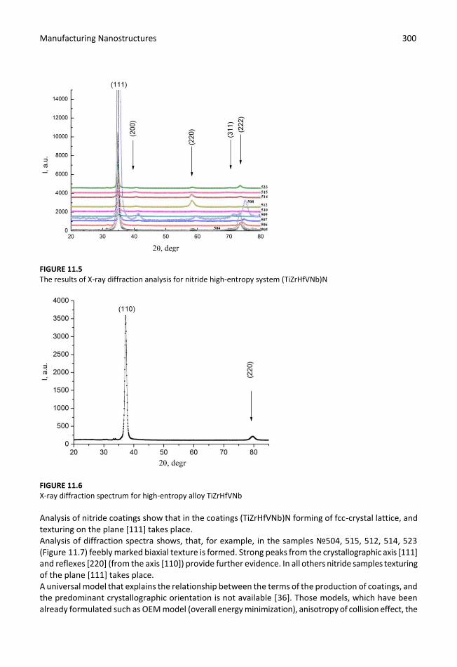
FIGURE 11.5 The results of X-ray diffraction analysis for nitride high-entropy system (TiZrHfVNb)N
FIGURE 11.6 X-ray diffraction spectrum for high-entropy alloy TiZrHfVNb
Analysis of nitride coatings show that in the coatings (TiZrHfVNb)N forming of fcc-crystal lattice, and texturing on the plane [111] takes place. Analysis of diffraction spectra shows, that, for example, in the samples №504, 515, 512, 514, 523 (Figure 11.7) feebly marked biaxial texture is formed. Strong peaks from the crystallographic axis [111] and reflexes [220] (from the axis [110]) provide further evidence. In all others nitride samples texturing of the plane [111] takes place. A universal model that explains the relationship between the terms of the production of coatings, and the predominant crystallographic orientation is not available [36]. Those models, which have been already formulated such as OEM model (overall energy minimization), anisotropy of collision effect, the

Manufacturing Nanostructures 301 301
extended structure zone model, explain only limited cases. However, when applied to experimental results, there are inconsistencies [36]. Thus, OEM model defines the following competing crystallographic planes in the nitride coatings with NaCl-like lattice: [200] plane with the lowest surface energy, the [111] plane with the lowest strain energy and the [220] plane with the lowest stopping energy. Thereby, developing of the plane [111], within the framework of OEM model, evidences about decreasing of stress energy. But according to Abadias et al. [37, 38] increasing of internal stresses is accompanied by increasing improvement in texture [111].
FIGURE 11.7 X-ray diffraction analysis for nitride high-entropy system coatings (TiZrHfVNb)N, obtained under Ub=-200 V
Thus, the following explanation is preferred [37]. Kinetic constraints (e.g. adatom mobility, collisional cascade effects, anisotropy in surface diffusivities) influence on the forming of preferable crystallographic orientation. On the one hand, the [111] plane is more close-packed, than the [220]. Consequently, the [220] plane have a high probability of survival. But on the other hand, the diffusion of metal adatoms on the surface [111] is less, than on the [220]. Thus, adatoms from the [220] can diffuse into the [111] plane, therefore, the [111] orientation can become preferred. Considering the evolution of the crystallographic planes orientation of samples №515, 512, 514, 523, 504, confirmation of the above explanation can be found. Increasing gas pressure in the working chamber leads to the increasing of the plasma ionization degree leading to a reduction of the diffusion length of the adatoms at the substrate during deposition. Initially immobile adatoms on the plane [111] hardly diffuse into the other plane, however, the incorporation (capturing) of adatoms [220] in the plane *111+ occurs. As a result, in the sample №515 peak intensities are very weak, practically no formed structure is observed. This sample the intensity of the plane [111] begins to dominate over the [220] plane (although the intensity of the plane [200] is approximately equal to intensity from the plane [111]). In sample №512, the intensity from the plane *220+ is a little bit more, than for the plane *111+. On increasing the pressure from 0.03 Pa to 0.2 Pa, and even to 0.23 Pa (for samples №514 and №523 respectively) on the X-ray diffraction spectra the increasing of peaks intensity from the plane [111] is
Manufacturing Nanostructures 302 302
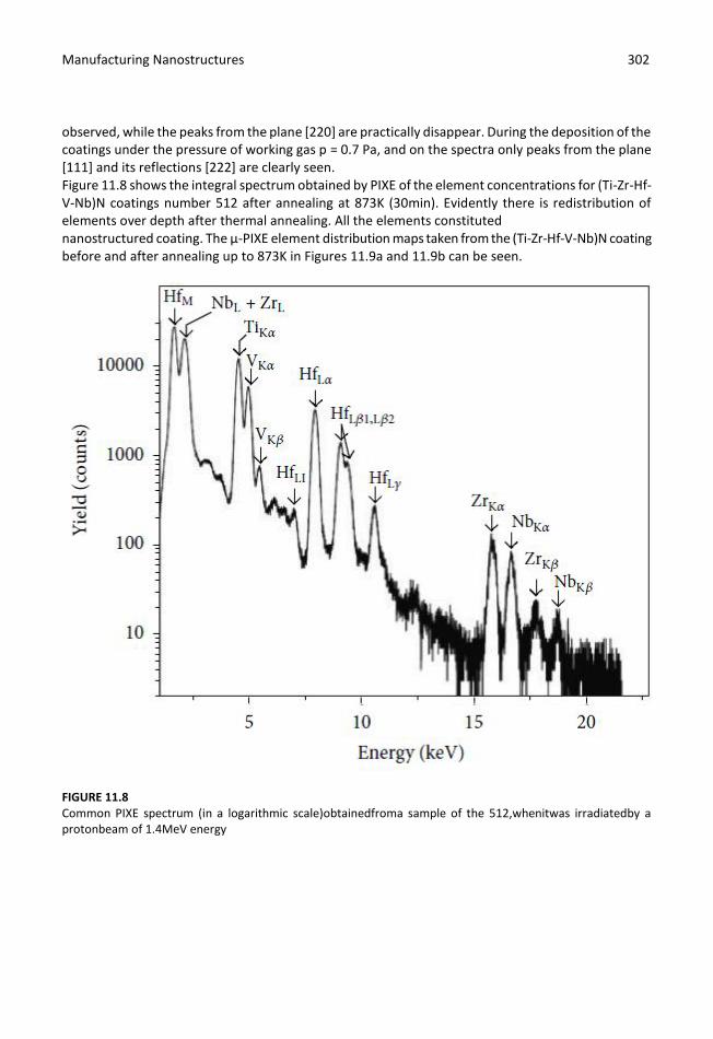
observed, while the peaks from the plane [220] are practically disappear. During the deposition of the coatings under the pressure of working gas p = 0.7 Pa, and on the spectra only peaks from the plane [111] and its reflections [222] are clearly seen. Figure 11.8 shows the integral spectrum obtained by PIXE of the element concentrations for (Ti-Zr-Hf-V-Nb)N coatings number 512 after annealing at 873K (30min). Evidently there is redistribution of elements over depth after thermal annealing. All the elements constituted nanostructured coating. The μ-PIXE element distribution maps taken from the (Ti-Zr-Hf-V-Nb)N coating before and after annealing up to 873K in Figures 11.9a and 11.9b can be seen.
FIGURE 11.8 Common PIXE spectrum (in a logarithmic scale)obtainedfroma sample of the 512,whenitwas irradiatedby a protonbeam of 1.4MeV energy

Manufacturing Nanostructures 303 303
a
b
FIGURE 11.9 Maps of the element distribution in the area of 2.5x2.5 μm (the raster of 50x50, the step size of 0.5 μm) for the sample 512 before (a) and after (b) annealing
Figure 11.9a shows the 3D map of the element distribution in the area of 2.5x2.5 μm for sample 512, with scanning step 0.5 μm. Elements are distributed almost evenly over the surface and in the bulk. Thermal annealing up to 873K(for 30min,at pressure in chamber 100 Pa) leads to the segregation of impurities at the grain interfaces, as shown in maps of these distributions see Figure 11.9b. All the elements forming the coating are arranged, and since the method PIXE is insensitive to nitrogen, the spectrum does not indicate it. The width of these interfaces is about 0.12 ± 0.25 μm, and the size of
large grains reaches up to 0.3–0.8 μm. XRD analysis and μ-PIXE with S-parameter, before and after
annealing, shows that in the structure of (Ti-Zr-Hf-V-Nb)N the grains of 0.3–0.8 μm with nanograins of
45–60 nm fragmented into them are formed. Dimensions of these nanograins were determined by XRD. After annealing, the impurities are segregated at the interfaces of large grains due to

Manufacturing Nanostructures 304 304
thermostimulated diffusion, and an interphase interlayer is formed at small grains as an agglutinating phase. In according to TEM investigations of the structural phase state of coatings with different contents of alloying elements (Si, B, Al), in the TiN system even at a high diffusion mobility of adatoms (i.e., at a
deposition temperature of 400–500°С) a textured two phase grain structure is formed in which the grains of submicron size (0.2–0.6 μm) are surrounded by low angle grain boundaries with angular
misorientations to 5° and by nanograins of size to 20–30 nm [39].
In this case, from the results of [3, 8, 39], as the content of low soluble (under equilibrium conditions) alloying elements increases and their concentration and/or diffusion mobility reaches a certain critical value, the enrichment of the boundaries of growing crystals by these elements occurs and, correspondingly, the grain size decreases [40]. This effect, along with the nonequilibrium deposition conditions, favors the formation of randomly oriented nanocrystallites. Electron diffraction from the coatings, obtained by C-PVD method, of the samples №504 and №508
(after thermal annealing 600°C during 30 minutes, 100 Pa) The effect of thermal high temperature annealing on the structural phase state of the coatings was investigated for samples №504 and №508. X-ray diffraction spectra for these coatings in the initial state (before thermal annealing) are shown on the Figure 11.5. X-ray strain measurements evidence, that the largest value of crystal lattice for sample №504 is equal а = 0.4420 nm, and for sample №508 а = 0.4380 nm (see Table 11.1). Microstructure and diffraction analysis, obtained by transmission electron microscopy for investigated samples after thermal annealing, are shown on the Figure 11.10. Analysis of diffraction data gave the lattice parameter of the samples after annealing. Thus, for the sample №504 а = 0,4327 nm, and for the sample №508 а = 0,4376 nm.
a b FIGURE 11.10 The microstructure and results of diffraction analysis, obtained by TEM method for the samples №504 (a) and №508 (b)
Thermal annealing thus leads to decreasing of the crystal lattice parameter, and the value of deformation also decreased, as evidenced by X-ray data tensometry.

Manufacturing Nanostructures 305 305
Stress state of (TiZrHfVNb)N nanostructured coatings The crystalline group method can be used to study the tension deformation state of textured coatings. It is based on the using of instructional techniques used to determine the state of stress-deformed single-crystal objects, namely: the measurement of interplanar spacings between different planes (hkl)
is conducted at certain angles of inclination *41+. α–sin2 dependencies, obtained for the samples
№506, 510 and 514 are shown in the Figure 11.11 (where a – is a crystal lattice parameter, – angle of the sample during the measurement). These samples were obtained under the same gas pressure P = 0.2 Pa, but under different voltage substrate bias (Table 11.1).
FIGURE 11.11
Dependences of α-sin2 obtained using the crystalline group method for the [111] axis of the nitride high-entropy
(TiZrHfVNb)N coating
The analysis shows that all coatings are under compressive stress state. The stress gradients are
evidenced along the film thickness: data measured at > 70° shows positive deviation from linear fit for samples №506 and №510. Less deviation is observed for sample №514 deposited at higher bias voltage (-200V). The slope of linear plots of the experimental data lines give the value of residual stresses in the coatings increases when using large values of negative substrate voltage during the deposition of nitride coatings.
Manufacturing Nanostructures 306 306
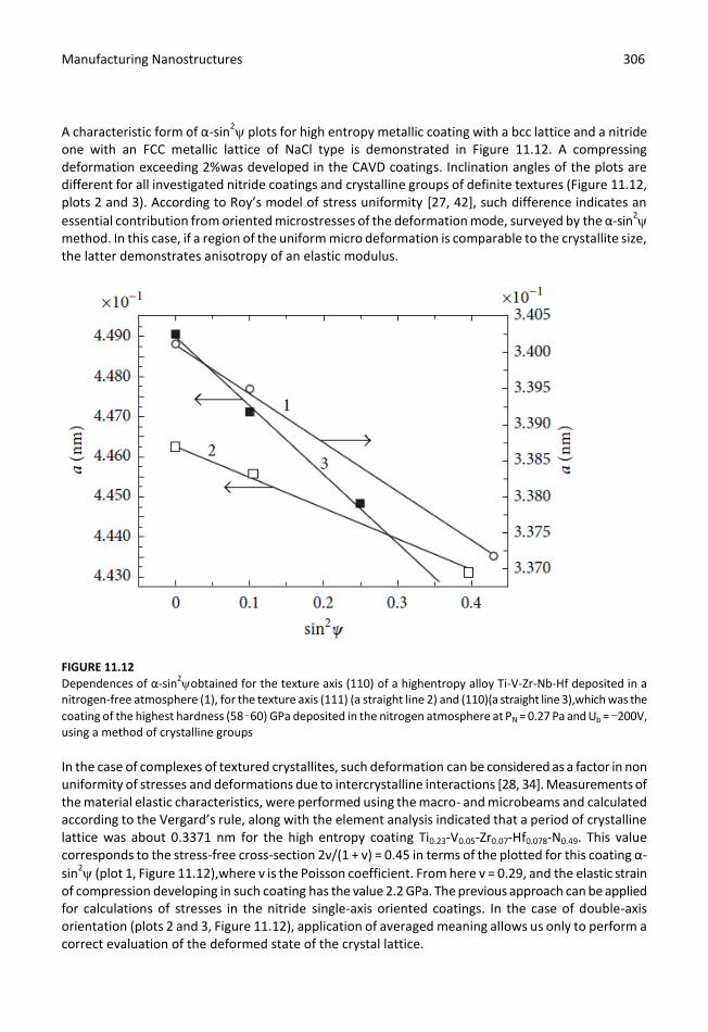
A characteristic form of α-sin2 plots for high entropy metallic coating with a bcc lattice and a nitride
one with an FCC metallic lattice of NaCl type is demonstrated in Figure 11.12. A compressing deformation exceeding 2%was developed in the CAVD coatings. Inclination angles of the plots are different for all investigated nitride coatings and crystalline groups of definite textures (Figure 11.12, plots 2 and 3). According to Roy’s model of stress uniformity [27, 42], such difference indicates an
essential contribution from oriented microstresses of the deformation mode, surveyed by the α-sin2
method. In this case, if a region of the uniform micro deformation is comparable to the crystallite size, the latter demonstrates anisotropy of an elastic modulus.
FIGURE 11.12
Dependences of α-sin2obtained for the texture axis (110) of a highentropy alloy Ti-V-Zr-Nb-Hf deposited in a
nitrogen-free atmosphere (1), for the texture axis (111) (a straight line 2) and (110)(a straight line 3),which was the
coating of the highest hardness (58–60) GPa deposited in the nitrogen atmosphere at PN = 0.27 Pa and Ub = −200V, using a method of crystalline groups
In the case of complexes of textured crystallites, such deformation can be considered as a factor in non uniformity of stresses and deformations due to intercrystalline interactions [28, 34]. Measurements of the material elastic characteristics, were performed using the macro- and microbeams and calculated according to the Vergard’s rule, along with the element analysis indicated that a period of crystalline lattice was about 0.3371 nm for the high entropy coating Ti0.23-V0.05-Zr0.07-Hf0.078-N0.49. This value corresponds to the stress-free cross-section 2ν/(1 + v) = 0.45 in terms of the plotted for this coating α-
sin2 (plot 1, Figure 11.12),where v is the Poisson coefficient. From here v = 0.29, and the elastic strain
of compression developing in such coating has the value 2.2 GPa. The previous approach can be applied for calculations of stresses in the nitride single-axis oriented coatings. In the case of double-axis orientation (plots 2 and 3, Figure 11.12), application of averaged meaning allows us only to perform a correct evaluation of the deformed state of the crystal lattice.

Manufacturing Nanostructures 307 307
PAS experiments demonstrated that positrons are well localized in the areas of low electron density (i.e., vacancy-type defects divacancies, conglomerates of various vacancies, vacancy complexes, and plus two or three interstitial atoms [31, 32, 43, 44]). As it follows from [32-35, 43, 44], the nanostructured materials, fabricated using the compaction, are good traps for positrons, which then annihilate with two or three components of the positron lifetime τ2, τ3.It is associated with positron annihilation at the grain interfaces, that is, the quasi-amorphous phase, in our case. The presented results (Figures 11.13a and 11.13b)) clearly indicate that the defect profiles (S-parameter) significantly differ for various deposition conditions; see, for example, samples510 and 512. At the same time, thermal annealing in a chamber with at high enough residual pressure (100Pa) leads to even greater changes of the S-parameter over the coating depth. The value of S-parameter for the sample 512decreases from 0.58-0.56 to 0.52-0.51 after annealing, and only when the analyzing energy of
positrons approaches (12.5–15) keV, it increases to 0.53. Analysis of S-parameter curve of the non-annealed sample 510 (13b) allows to conclude that positron-sensitive defects are almost absent throughout the whole coating depth. This means that annihilation occurred mainly with the electrons of the defect-free areas.
a b FIGURE 11.13 Dependencies of the S-parameter of the annihilation peak Doppler broadening measured over (Ti-Zr-Hf-V-Nb)N coating depth, for the samples 512 (a) and 510 (b), after deposition and annealing at 873 K, (100 Pa)
Therefore, the value of S-parameter was minimal and equal to 0.49. As a result of annealing at 873 K, the value of S-parameter increased significantly to 0.53 in the surface layer. The value of S-parameter further increased at positron energy of 14 to 17 keV and approached the maximum possible value 0.59.It should be mentioned that the S-parameter depends on both the concentration and the type of vacancy defects, at which positrons are captured and subsequently annihilate there in the areas of low electron density [32, 43, 44]. Since a grain size of the nanostructured coatings is smaller than a length of positron diffusion track in defect free nanograin, all positrons can reach the grain surface and consequently the interfaces. In this case, most of the volume of available information concerns the defects in the interfaces and triple or more joints. Since the grain size in our experiments varies from 40 to 60 nm, the volume fraction of the
Manufacturing Nanostructures 308 308
interfaces may reach 30 to 35 vol.%, and the interfaces of triple joints may be about 5 to 10 vol.%, and then almost all positrons have to be captured along the interfaces [27]. According to results presented in [32], the total fraction of interfaces can be evaluated as
L
S
L
SLSVS
3)]/(3[1
21
(1)
where L is the grain size and S is the interface width (the near-interface zone). A fraction of the inherent grain interfaces is
21
)]/(3[
L
SLSVI
(2) And a fraction of triple joints is
111 IST VVV (3)
If the distance between the defects is shorter than the positron diffusion length, all positrons have to be captured by defects; that is, we observed the capture saturation. In this case, the positron lifetime spectrum contains only one component [43, 44], and the S-parameter of Doppler broadening seems to have a maximum value. RBS (Figures 11.2a and 11.2b) and EDX analyses for the samples 510 (for which the value of the elastic stress in the initial state is much lower than for sample 512) indicated that two peaks are formed on
the curve of S-parameter when the energy of the positron beam is (3 ÷ 5) keV and (14 ÷ 17) keV. This can be explained by the increased diffusion process of both nitrogen and oxygenatoms near the surfaces of the samples 510. This indicates the appearance of new channels for the annihilation of positrons, which are more efficiently attracted by defects, which appeared at the interface as a result of annealing and formed the new quasi-amorphous and nanostructured phases of nitrides. This conclusion is supported by the results of PIXE-μ analysis, which indicated that an oxide film was formed on the surface, and therefore the value of S-parameter increased. In the coating depth, the elements are redistributed, which confirmed the assumption about the end of the process of spinodal segregation and the formation of new phases along nanograin interfaces [27, 28, 33-35]. The grain growth during annealing is due to mechanism of structural relaxation. The segregation of nitrogen at the grain interfaces hampers the growth of nanocrystals. Evaluation of the nanograins size by XRD, according to the Debye-Scherrer, gave the nanograins size of
55–58 nm for samples 512, which did not change after thermal annealing. Evaluation of the diffusion
length of positrons was L +≈ 100 nm, which was essentially longer than the size of nanograins. According to the conventional interpretation, the nanopores are primarily placed at the lines of intersection of three or more interfaces. Thus, the ratio of intensities of the positron lifetime components decrease with increasing crystallite size confirmed by the theoretical and experimental studies [27, 32, 43, 44]. Therefore, reduction of the S-parameter (sample 512) may be connected to the annealing of interface vacancies, resulting in a decrease of the S-parameter intensity [9, 45, 46]. Moreover, additional nanopores may appear due to the vacancy agglomeration taking place in the process of crystallite growing, even if the latter is not very significant. This may result in the increase of

Manufacturing Nanostructures 309 309
the S-parameter. This was reported in the work of [35], where the intensity of the second component of positron lifetime increased. RBS (Figures 11.2a and 11.2b) and EDX analyses, the strongly structured coatings number 512 with a
high level of compressive strain in the as-deposited states (−2.76%) demonstrate the high oxidation resistance after annealing. This occurred due to low oxygen diffusion to the coating depth and a high degree of filling of the octahedral interstitials by nitrogen atoms during the deposition of coating under conditions of high nitrogen pressure in the chamber. This system does not form a nitride interlayer between nanograins, due to the low diffusion resulting from high compressive stresses. Annealing temperature is insufficient or the energy of atoms is too low to form the interlayer. The main channel allowing the nitrogen atoms to sink for the formation of the nitrideinterlayer is the interphase “coating-substrate” boundary (see the S-parameter curve of the maximum value 0.53 at energy of analyzing positron beam of 13-14 keV). Tribological properties Microindentation was used to investigate the microhardness of samples №506, 507 and 514, under with increasing load from 500 mN to 1.5 mN. Values of microhardness, Young modulus, and the deviations of measured values were obtained as a result of the investigation. Figure11.14 shows the change of microhardness of the coatings from a substrate voltage, for three identical values of the indenter load (0.5 N, 0.75 N and 1 N).
a b FIGURE 11.14 Graphs of microhardness change (a) and Young modulus change (b) of nitride high-entropy alloys under indenter load change
From these dependencies increasing of the negative substrate voltage bias (from -50V (№507) to -200V (№514)) leads to increasing of microhardness (Figure 11.14a), and Young modulus (Figure 11.14b). Points on the graph indicate values of measured parameters (Y axis) for the corresponding samples (X axis). Trend lines (for the corresponding loads) show the character of measurement values change (in our case – increasing of microhardness and Young modulus during the increasing of Ub). Increasing negative voltage substrate bias leads to increasing of ions number, bombarding the surface of the coating, and thus, to increasing of plasma density. This causes decreasing of the grain size in the

Manufacturing Nanostructures 310 310
coatings, grain boundaries in the coating, increase in the compressive residual stresses and increasing of point defects number. This promotes the decreasing of dislocations advancements, and, thus, leads to increasing of the coatings’ microhardness. Vickers hardness was measured for the samples №505, 507, 509, 512, 523 under the loads 0.05 N and 0.1 N. Figure 11.15 shows bar graphs with average values of Vickers hardness for all samples, in increasing order of the substrate voltage values and a working gas pressure.
FIGURE 11.15 Bar graphs which shows changes of Vickers microhardness for the investigated samples
The bar graphs, do not give us an opportunity to consider the influence of deposition parameters on the Vickers microhardness, because simultaneously there are two changing parameters – Ub and P. These two factors influence the mechanical characteristics at the same time, so it’s difficult to estimate their influence on the hardness separately. For example, while comparing microhardness for samples №507 and №505, that during the increasing of Ub from -50 V (for the sample №507) to -110 V (for the sample №505) the increasing of microhardness is observed. The hardness data for more than two samples is needed, to find out how the change of deposition parameters influences on the microhardness change. But nevertheless, shown bar graphs give a general representation, and it is clearly seen, that nitride high-entropy alloys (TiZrHfVNb)N demonstrate high values of mechanical properties. Figure 11.16 shows microphotograph of the pyramidal indenter stamp on the surface of the one of the coating.
Figure 11.16 Images of pyramidal indenter stamps for sample №512

Manufacturing Nanostructures 311 311
Sizes of indenter stamps (diagonal length) is used to determine the numerical value of the microhardness of coatings, according to Vickers. According to [23, 24, 47], increasing of content of low-soluble alloying elements, upon reaching their critical concentration and/or diffusion mobility, leads to enrichment of interfaces of growing crystals with these elements (taking into account the values of mixing entropy of separate nitrides (Table 11.2)), and the total entropy of all metals and nitrides on its basis included to the coatings), and to corresponding decrease of the grain size [48]. TABLE 11.2 Enthalpies of formation (ΔH) of the five binary nitrides
TiN VN ZrN HfN NbN
ΔH, KJ/mole −337.7 −217.2 365.3 −373 −234.7
This effect, along with the nonequilibrium deposition conditions, promoted the formation of randomly oriented nanocrystallites. The maximum nanohardness of𝐻 =58 GPa was obtained also for the samples 512. Elastic modulus for these samples reached the value of E = 618 GPa. For samples 509 and 510,
hardness values were of little lower rates−52 GPa and 46 GPa, respectively. Analysis of the wear byproducts, wear track structure (on the sample), and wear spots (on counterface ball) was provided along with microscopic study of the wear tracks structure on the coating surface and the change of wear spots on the ball. Measurement of the vertical section of wear tracks was performed by profilometer in four diametrically and orthogonally opposite fields and determined the average cross-sectional area and wear tracks. Figure 11.17a presents the results of tribological wear test of the steel substrate.
FIGURE 11.17 (a) Results of tribological tests of steel substrate (steel 45); (b) The results of tribological tests of the “steel 45+coating (Ti-HF-Nb-Zr-V)N-Al2O3counterface”

Manufacturing Nanostructures 312 312
Vacuum-arc coatings of Ti-Zr-Hf-Nb-V (4.0mm thick) were deposited in the nitrogen reaction gas environment on the polished steel disc. The results of the friction tests showed an increase in the surface roughness due to the drop component of the plasma flow (see Figure 11.17b and Table 11.3). TABLE 11.3 Tribological characteristics of the different systems based on Ti, Zr, Hf, Nb, V, N
Sample Friction coefficient, μ Wear factor mm3 x H
-1 x mm
-1
Initial During experiment Of counterface (x10
-5)
Of sample (x10
-5)
Coatings Ti-Hf-Nb-Zr-V-N
0.221 1.030 1.12 0.027
Steel 45 0.204 0.674 0.269 35.36
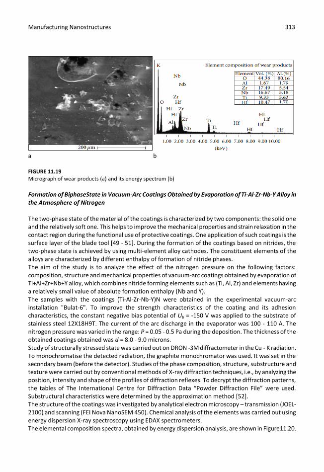
Deposition on the substrate of steel 45 provides an increased durability, thus reducing the wear of steel. The study of friction tracks can give the information about the mechanism of wear. Figure 11.18 shows photographs of friction tracks in vacuum-arc coating (Ti-HF-Nb-Zr-V)N. Results of the study of wear products in the friction process for the coating (Ti-HF-Nb-Zr-V)NAl2O3counterface are shown in Figure 11.19.
a b FIGURE 11.18 Photographs of the surface morphology of friction: (a) general view and (b) friction track
Manufacturing Nanostructures 313 313
a b FIGURE 11.19 Micrograph of wear products (a) and its energy spectrum (b)
Formation of BiphaseState in Vacuum-Arc Coatings Obtained by Evaporation of Ti-Al-Zr-Nb-Y Alloy in the Atmosphere of Nitrogen The two-phase state of the material of the coatings is characterized by two components: the solid one and the relatively soft one. This helps to improve the mechanical properties and strain relaxation in the contact region during the functional use of protective coatings. One application of such coatings is the surface layer of the blade tool [49 - 51]. During the formation of the coatings based on nitrides, the two-phase state is achieved by using multi-element alloy cathodes. The constituent elements of the alloys are characterized by different enthalpy of formation of nitride phases. The aim of the study is to analyze the effect of the nitrogen pressure on the following factors: composition, structure and mechanical properties of vacuum-arc coatings obtained by evaporation of Ti+Al+Zr+Nb+Y alloy, which combines nitride forming elements such as (Ti, Al, Zr) and elements having a relatively small value of absolute formation enthalpy (Nb and Y). The samples with the coatings (Ti-Al-Zr-Nb-Y)N were obtained in the experimental vacuum-arc installation "Bulat-6". To improve the strength characteristics of the coating and its adhesion characteristics, the constant negative bias potential of Ub = -150 V was applied to the substrate of stainless steel 12X18H9T. The current of the arc discharge in the evaporator was 100 - 110 A. The nitrogen pressure was varied in the range: P = 0.05 - 0.5 Pa during the deposition. The thickness of the obtained coatings obtained was d = 8.0 - 9.0 microns. Study of structurally stressed state was carried out on DRON -3M diffractometer in the Cu - K radiation. To monochromatise the detected radiation, the graphite monochromator was used. It was set in the secondary beam (before the detector). Studies of the phase composition, structure, substructure and texture were carried out by conventional methods of X-ray diffraction techniques, i.e., by analyzing the position, intensity and shape of the profiles of diffraction reflexes. To decrypt the diffraction patterns, the tables of The International Centre for Diffraction Data “Powder Diffraction File” were used. Substructural characteristics were determined by the approximation method [52]. The structure of the coatings was investigated by analytical electron microscopy – transmission (JOEL-2100) and scanning (FEI Nova NanoSEM 450). Chemical analysis of the elements was carried out using energy dispersion X-ray spectroscopy using EDAX spectrometers. The elemental composition spectra, obtained by energy dispersion analysis, are shown in Figure11.20.

Manufacturing Nanostructures 314 314
The structural state study, carried out by the X-ray diffraction method, has shown that the coatings obtained at the lowest pressure (0.05 Pa) have a phase with bcc lattice as a crystalline phase, which is typical of the structure of high entropy alloy without formation of own nitride lattice [53]. Apparently nitrogen present in the coating in this case creates formations with amorphous structure, observed as a “halo” in the range of angles 2θ ≈ 31 - 42 degrees with a maximum at an angle 2θ ≈ 36 degrees. Analysis of the spectra in the used range of pressures, the composition of the nitrogen component in the coatings varied from 7.11 at. % (at P = 0.05 Pa) and 1.26 at. % (at P = 0.3 Pa) to 35.42 at. % at P = 0,5 Pa. The content of metal components for Al:Ti:Zr:Nb:Y was observed in proportion of 5:9:10:5:6 respectively.
а
b c FIGURE 11.20 Energy dispersion spectra of the coatings, obtained at different nitrogen pressures: а – P = 0.05 Pa, b – P = 0.3 Pa, c – P = 0.5 Pa
The size of the bcc phase crystallites is small at 7.7 nm. If estimated the content of the phases in the coating by the ratio of the integral intensities, than it is close to 2/1, respectively, for the bcc phase and for phase in amorphous-like condition. For coatings produced at a higher pressure of working atmosphere of 0.3 Pa (Curve 2 in Figure 11.21) the crystalline state becomes apparent for a component phase with a bcc crystalline lattice as well as for the nitride (Ti-Al-Zr-Nb-Y)N phase with fcc lattice (structural type NaCl). The size of the crystallites of the bcc phase was about 11.5 nm and for the nitride fcc phase it was about 5 nm. Lattice period, determined by the position of maximum of diffraction peak, was 0.462 nm. The ratio of bcc and fcc phases is close to 1/2. Analysis of the third spectrum characterizing the coatings obtained at the highest pressure of P = 0.5 Pa, has a higher degree of crystallinity of the constituent phases with the determining content of the

Manufacturing Nanostructures 315 315
fcc phase (the content of bcc and fcc components has a ratio of 1/3). The size of bcc phase crystallites is about 10 nm and the size of nitride fcc phase crystallites is close to 7 nm. Defined by the position of maximum, the period of the lattice is 0.453 nm.
FIGURE 11.21 Areas of diffraction spectra of the coatings deposited at different pressures of nitrogen: curve 1 – P = 0.05 Pa, 2 – P = 0.3 Pa, 3 – P = 0.5 Pa
Analysis shows that the appearance of bcc phase in the coating is determined mainly by the droplet phase, which has a crystal structure at all pressures of nitrogen during the deposition process. Fcc crystal lattice corresponds to the nitride phase. At increasing pressure, the size of the ordering regions increases. It varies from amorphous-like state at the lowest pressure with the content of nitrogen atoms in the coating of about 12 at. % to nanocluster state with the size of ranked structural formations of 5 nm at an average pressure when the content of nitrogen atoms in the coating is 26 at. %. The nanocrystalline state at the maximum pressure with the content of nitrogen atoms in the coating of 36 at. %. Figure 11.22 shows the image of the microstructure of the coating based on (Ti-Al-Zr-Nb-Y)N and micro diffraction from the selected area (see Figure 11.22a). Micro diffraction obtained from this area corresponds to the fcc lattice with a period close to the one obtained by X-ray analysis.

Manufacturing Nanostructures 316 316
FIGURE 11.23 Image of microstructure of the coating based on (Ti-Al-Zr-Nb-Y)N (a) and microdiffraction pattern (b), obtained at nitrogen pressure P = 0.3 Pа
Measurement of universal mechanical characteristic of the coating as hardness showed that with the increase of pressure of nitrogen the hardness of samples varies from 34 GPa at the lowest pressure to 49 GPa at the highest pressure and the content of nitrogen of 36 at. %. The structure of the coating formed at low pressure of the nitrogen atmosphere is the least thermodynamically stable, which determines the lowest hardness of the coatings. Increasing the pressure brings the system to a more stable state with a biphase structure, resulting in increased hardness of up to 49 GPa.
Conclusions The results revealed mechanisms of formation of interfaces in multicomponent coatings and formation of the stress states of nanocrystals, as well as their effect on thermal diffusion of nitrogen and oxygen atoms. By changing the deposition conditions, it is possible to influence the thermal stability and hardness of multicomponent nanostructured coatings. The effect of defect migration on hampering the nanocrystal growing was considered, when the annealing temperature increased. Highentropy nitride alloys and nanostructured coatings on their base contained only the single-phase solid solutions. The structure was composed of the submicron grains of 0.3–0.8 μm, at the interfaces of which the interlayers of impurity atoms were formed. At the same time, the fragmented nanograin structures of 40–60 nm size with subgrains of the nitride phases were formed in the submicron grains. The slow diffusion originating from the higher packing density because of the packing of atoms with different sizes made the effective diffusion distances very short, which led to the enhanced difficulty of grain growth. Regarding the lattice decline, the following three possible factors must be considered: composition variation, phase separation, and residual stress.

Manufacturing Nanostructures 317 317
Nitride coatings (TiZrHfVNb)N, based on high-entropy alloys have been investigated. They formed single-phase structure with fcc crystal lattice and predominant texture [111]. Increasing of negative voltage substrate bias during the deposition of the coatings promoted the formation of single-axe structure, with simultaneous growth of its perfection. High-temperature thermal annealing did not cause significant changes tothe structure and phase state, but a slight change (decrease) of the lattice parameter, and of residual stresses is observed. Coatings, obtained under high values of negative voltage substrate bias, demonstrate high level of residual stresses. Decreasing of voltage bias leads to decreasing of the residual stresses in the investigated coatings. Increasing of substrate bias could enhance the microhardness of (TiZrHfVNb)N nitride coatings from 24,78 GPa to 27,36 GPa. But increasing of working gas in opposite, leads to reduction of microhardness. Changing of deposition parameters of nitride high-entropy alloys (TiZrHfVNb)N influenced the physical, mechanical and structural properties of investigated coatings.
References
1. J.-W. Yeh, Y.-L. Chen, S.-J. Lin, S.-K. Chen, High-entropy alloys, a new era of exploitation, Mater.
Sci. Forum; 2007; 560, 1-9.
2. A. D. Pogrebnjak, Structure and properties of nanostructured (Ti-Zr-Hf-V-Nb)N coatings, Journal
of Nanomaterials; 2013, Article ID 780125, 2013;1-12 .
3. J. Musil, Hard nanocomposite coatings: Thermal stability, oxidation resistance and toughness,
Surf. Coat. Tech.2012; 207, 50-65.
4. A. D. Pogrebnyak, A. P. Shpak, N. A. Azarenkov, V. M. Beresnev, Structures and properties of
hard and superhardnanocomposite coatings, Phys.-Usp.; 2009, 52, № 1, 29-54
5. A. D. Pogrebnyak, A. G. Ponomarev, D. A. Kolesnikov, V. M. Beresnev, F. F. Komarov,
S. S. Mel’nik, M. V. Kaverin, Effect of mass transfer and segregation on the formation of
superhard nanostructured Ti-Hf-N(Fe) coatings, Techn. Phys. Lett.; 2012, 38, N. 7, 623-626,
6. A. D. Pogrebnjak, V. M. Beresnev, A. A. Demianenko, V. S. Baidak, F. F. Komarov, M. V. Kaverin,
N. A. Makhmudov, D. A. Kolesnikov, Adhesive strength, superhardness, and the phase and
elemental compositions of nanostructured coatings based on Ti-Hf-Si-N, Phys. Solid State;
2012, 54, N 9., 1882-1890
7. A. D. Pogrebnjak, A. P. Shpak, V. M. Beresnev, D. A. Kolesnikov, Y. A. Kunitskii, O. V. Sobol,
V.V. Uglov, F. F. Komarov, A. P. Shypylenko, N. A. Makhmudov, A. A. Demyanenko, V. S. Baidak,
V. V. Grudnitskii, Effect of thermal annealing in vacuum and in air on nanograin sizes in hard
and superhard coatings Zr-Ti-Si-N, J. Nanosci. Nanotechn.; 2012, 12, N 12, 9213-9219.
8. A. D. Korotaev, D. P. Borisov, V. Yu. Moshkov, S. V. Ovchinnikov, K. V. Oskomov, Yu. P. Pinzhin,
V. M. Savostikov, A. N. Tymentsev,Nanocomposite and nanostructured superhard Ti-Si-B-N
coatings, Russian Physics Journal; 2007, 50, № 10, 969-979.
9. A. D. Pogrebnjak, O. V. Sobol, V. M. Beresnev, P. V. Turbin, G. V. Kirik, N. A. Makhmudov,
M. V Il'yashenko1, A. P. Shypylenko, M. V. Kaverin, M. Yu. Tashmetov, A. V. Pshyk, Phase
composition, thermal stability, physical and mechanical properties of superhard on base Zr-Ti-

Manufacturing Nanostructures 318 318
Si-N nanocomposite coatings, Nanostructured materials and Nanotechnology IV: Ceramic Eng.
Sci. Proc.; 2010, 31, N. 7, 127- 138.
10. S. Veprek, M.G.J. Veprek-Heijman, Limits to the preparation of superhardnanocomposites:
Impurities, deposition and annealing temperature, Thin Solid Films; 2012, 522, 274-282
11. C.-H. Lai, M.-H. Tsai, S.-J. Lin, J.-W. Yeh, Influence of substrate temperature on structure and
mechanical, properties of multi-element (AlCrTaTiZr)N coatings, Surf. Coat. Technol.;2007, 201,
6993-6998
12. P. K. Huang, J. W. Yeh, Effects of nitrogen content on structure and mechanical properties of
multi-element (AlCrNbSiTiV)N coating, Surf. Coat. Technol.; 2009, 203, 1891-1896.
13. Sh.-Y. Chang, D.-Sh.Chen, 10-nm-thick quinary (AlCrTaTiZr)N film as effective diffusion barrier
for Cu interconnects at 900°C, Appl. Phys. Lett.;2009, 94, art. 231909.
14. S.-Ch. Liang, Z.-Ch. Chang, D.-Ch. Tsai, Y.-Ch. Lin, H.-Sh. Sung, M.-J. Denga, F.-Sh. Shieu, Effects
of substrate temperature on the structure and mechanical properties of (TiVCrZrHf)N coatings,
Appl. Surface Sci.;2011, 257, 7709-7713.
15. Z.-Ch. Chang, Sh.-Ch. Liang, Sh. Han Effect of microstructure on the nanomechanical properties
of TiVCrZrAl nitride films deposited by magnetron sputtering, Nuclear Instrum. Methods in
Phys. Res. B.; 2011, 269, 1973-1976.
16. R. Krause-Rehberg, A. D. Pogrebnyak, V. N. Borisyuk M. V. Kaverin, A. G. Ponomarev,
M. A. Bilokur, K. Oyoshi, Y. Takeda, V. M. Beresnev, O. V. Sobol’, Analysis of local regions near
interfaces in nanostructured multicomponent (Ti-Zr-Hf-V-Nb)N coatings produced by the
cathodic-arc-vapor-deposition from an arc of an evaporating cathode, Physics of Metals and
Metallography; 2013, 114, № 8, 672-680.
17. Aj. K. Mishra, S. Samal, Kr. BiswasSolidification behaviour of Ti–Cu–Fe–Co–Ni high entropy
alloys, Trans. Indian Inst. Metals.; 2012, 65, N 6, 725-730.
18. Ch.-W. Tsai, S.-W. Lai, K.-H. Cheng, M.-H. Tsai, A. Davison, Ch.-H. Tsau, J.-W. Yeh, Strong
amorphization of high-entropy AlBCrSiTi nitride film, Thin Solid Films; 2012, 520, N 7, 2613-
2618.
19. S. A. Firstov, V. F. Gorban', N. A. Krapivka, E. P. Pechkovskiy, Hardening and mechanical
properties of as-cast high-entropy alloys, Composites and Nanostructures; 2011, 2, 5-20 (in
Russian).
20. V. Braic, M. Balaceanu, M. A. Braic A. Vladescu, S. Panseri, A. Russo, Characterization of multi-
principal-element (TiZrNbHfTa)N and (TiZrNbHfTa)C coatings for biomedical applications,
J. Mech. Behavior Biomed. Mater.; 2012, 10, 197-205.
21. O. V. Sobol’, A. D. Pogrebnjak, and V. M. Beresnev, “Effect of the preparation conditions on the
phase composition, structure, and mechanical characteristics of vacuum-Arc Zr-Ti-Si-N
coatings,” The Physics of Metals and Metallography; 2011, vol. 112, no. 2, pp. 188–195.
22. J. Musil, J. Vlcek,ˇ and P. Zeman, “Hard amorphous nanocom-posite coatings with oxidation
resistance above 1000∘C,” Advances in Applied Ceramics; 2008, vol.107, no. 3, pp. 148–154.
23. A. D. Korotaev, V. D. Borisov, V. Yu. Moshkov, C. V. Ovchinnikov, Yu. P. Pinzhin,
A. N. Tyumentsev, Elastic stress state in superhardmultielement coatings, Phys. Mesomech.;
2009, 12, 269-279.

Manufacturing Nanostructures 319 319
24. A. D. Pogrebnjak, V. M. Beresnev, D. A. Kolesnikov et al., “The effect of segregation and
thermodiffusion on the formation of interfaces in nanostructured (Ti-Hf-Zr-V-
Nb)Nmultielement coatings,” Technical Physics Letters; 2013, vol. 39, no. 3, pp. 280–283.
25. O. V. Sobol’, A. A. Andreev, V. F. Gorban et al., “Reproducibility of the single-phase structural
state of the multielement high-entropy Ti-V-Zr-Nb-Hf system and related superhard nitrides
formed by the vacuum-arc method,” Technical Physics Letters; 2012, vol. 38, no. 7, pp. 616–
619.
26. http://www.simnra.com.
27. R. Krause-Rehberg and H. S. Leipner, Positron Annihilation in Semiconductors, vol. 127 of Solid-
State Sciences, Springer, Berlin, Germany, 1999.
28. A. D. Pogrebnjak, A. G. Ponomarev, D. A. Kolesnikov et al., “Effect of mass transfer and
segregation on the formation of superhard nanostructured Ti-Hf-N(Fe) catings,” Technical
Physics Letters; 2012, vol. 38, no. 7, pp. 623–626.
29. A. D. Pogrebnjak and V. M. Beresnev, NanocoatingsNanosystems Nanotechnologies, Bentham
Science, 2012.
30. V.I. Lavrentiev,A.D.Pogrebnjak“High-dose ion implantation into metals” Surface and Coatings
Technology, 1998, vol. 99 (1-2), pp. 24-32
31. H. E. Shaefer, “Investigation of thermal equilibrium vacancies in metals by positron
annihilation,” Physica Status Solidi; 1987, vol. 102, no. 1, pp. 47–65.
32. V. I. Lavrent’yev, A. D. Pogrebnjak, and R. Sandrik, “Evolution of vacancy defects in the surface
layers of a metal irradiated with a pulsed electron beam,” JETP Letters; 1997, vol. 65, no. 8, pp.
651–655.
33. S. Veprek, “The search for novel, superhard materials,” Journal of Vacuum Science &
Technology A; 1999, vol. 17, no. 5, pp. 2401–2421.
34. J. Musil, “Hard and superhard nanocomposite coatings,” Surface and Coatings Technology;
2000, vol. 125, no. 1–3, pp. 322–330.
35. A. I. Gusev, Nanomaterials, Nanostructures and Nanotechnol-ogy, Fizmatlit, Moscow, Russia,
2005.
36. Mahieu, D. Depla, Reactive sputter deposition of TiN layers: modelling the growth by
characterization of particle fluxes towards the substrate; 2009, J. Phys. D: Appl. Phys., 42,
053002.
37. G. Abadias, Y. Y. Tse, Ph. Guérin, V. Pelosin Interdependence between stress, preferred
orientation, and surface morphology of nanocrystallineTiN thin films deposited by dual ion
beam sputtering, J. Appl. Phys.; 2006, 99, 113519-1-113519-13.
38. G. Abadias, L. E. Koutsokeras, A. Siozios, P. Patsalas, Stress, phase stability and oxidation
resistance of ternary Ti–Me–N (Me=Zr, Ta) hard coatings, Thin Solid Films; 2013, 538, 56-70.
39. A.D. Pogrebnjak, I.V.Yakushchenko, A.A.Bagdasaryan, O.V.Bondar, R. Krause-Rehberg, G.
Abadias, P. Chartier, K. Oyoshi, Y.Takeda, V.M. Beresnev, O.V.Sobol, "Microstructure, physical
and chemical properties of nanostructured (Ti-Hf-Zr-V-Nb)N coatings under different
deposition conditions", Materials Chemistry and Physics, 2014, vol. 147(3), pp.1079-1091

Manufacturing Nanostructures 320 320
40. P. Misaelides, A. Hadzidimitrion, F. Noli, E. Pavlidou, A. D. Pogrebnjak, “Investigation of the
characteristics and corrosion resistance of Al2O3/TiN coatings”, Appl. Surf. Sci.; 2006, 252,
8043-8049.
41. C. Genzel, W. Reinmers A study of X-ray residual stress gradient analysis in thin layers with
strong fibre texture, Phys. Stat. Solidi: A-Applied Research; 1998, 166, 751-762.
42. N. A. Azarenkov, O. V. Sobol’, A. D. Pogrebnjak, and V. M. Beresnev, Engineering Vacuum-
Plasma Coatings, National University, Kharkov, Ukraine, 2011.
43. S. V. Rempel’ and A. I. Gusev, “Surface segregation in decom-posing carbide solid solutions,”
JETP Letters; 2008, vol. 88, no. 7, pp. 435–440.
44. R. Wurschum,¨ P. Farber, R. Dittmar, P. Scharwaechter, W. Frank, and H.-E. Schaefer, “Thermal
vacancy formation and self-diffusion in intermetallic Fe3Si nanocrystallites of nanocomposite
alloys,” Physical Review Letters; 1997,vol. 79, no. 24, pp. 4918– 4921.
45. A. D. Pogrebnjak, S. M. Ruzimov, D. L. Alontseva et al., “Structure and properties of coatings on
Ni base deposited using a plasma jet before and after electron a beam irradiation,” Vacuum;
2007, vol. 81, no. 10, pp. 1243–1251.
46. A. D. Pogrebnjak, O. G. Bakharev, N. A. Pogrebnjak Jr. et al., “Certain features of high-dose and
intensive implantation of Al ions in iron,” Physics Letters A;2000, vol. 265, no. 3, pp. 225–232.
47. J. Musil, “Hard nanocomposite coatings: thermal stability, oxidation resistance and toughness,”
Surface and Coatings Technology; 2012, vol. 207, pp. 50–65.
48. V. Ivashchenko, S.Veprek, A.Pogrebnjak, B.Postolnyi, "First-principles quantum molecular
dynamics study of TixZr 1-xN(111)/SiNyheterostructures and comparison with experimental
results",Science and Technology of Advanced Materials, 2014 vol.15(2), a.n. 025007
49. Pogrebnjak A.D., Beresnev V.M., Kolesnikov D.A., Bondar O.V., Takeda Y., Oyoshi K., Kaverin
M.V., Sobol O.V., Krause-Rehberg R., Karwat C. Multicomponent (Ti-Zr-Hf-V-Nb)N
Nanostructure Coatings Fabrication, High Hardness and Wear Resistance //
ActaPhysicaPolonica, A; 2013, Vol. 123, No. 5. – P. 816-818.
50. A.D. Pogrebnjak, Yu.A. Kravchenko, S.B. Kislitsyn, Sh.M. Ruzimov, F. Noli, P. Misaelides, A.
Hatzidimitriou "TiN/Cr/Al2O3 and TiN/Al2O3 hybrid coatings structure features and properties
resulting from combined treatment",Surface and Coatings Technology, 2006, vol.201(6),
pp.2621-2632
51. Azarenkov N.A., Sobol O.V., Beresnev V.M., Pogrebnyak O.D., Kolesnivov D.A., Turbin P.V.,
Torianyk I.M. Vacuum-plasma coatings based on multielement nitrides // Metal physics and
modern technologies; 2013, Vol. 35, No. 8. P. 1061-1084.
52. Palatnik L.S., Fuchs M.Ya, Kosevich V.M. Formation mechanism and substructure of condensed
films. – M.: Science, 1972. – 320 p.
53. A.D. Pogrebnjak, D. Eyidi, G. Abadias, O.V. Bondar, V.M. Beresnev, O.V. Sobol, "Structure and
properties of arc evaporated nanoscaleTiN/MoN multilayered systems", International Journal
of Refractory Metals and Hard Materials, 2015, vol. 48, pp. 222-228