Industrial applications of low-temperature plasma physics - UCLA
12
Industrial applications of low-temperature plasma physics* Francis F. Chent University of California, Los Angeles, California 900241594 (Received14 November 1994; accepted 6 February 1995) The applicationof plasma physics to the manufacturing and processing of materials may be the new frontier of our discipline. Already partially ionized discharges are used in industry, and the performance of plasmas has a large commercialand technological impact. However,the science of low-temperature plasmas is not as well developed as that of high-temperature, collisionlessplasmas. In this paperseveralmajor areas of applicationare described and examples of forefront problemsin each are given. The underlying thesis is that gas discharges have evolved beyond a black art, and that intellectually challenging problems with elegant solutions can be found. 0 I995 American institute of Physics. 1. INTRODUCTION During the past four decades, the science of high- temperature and collisionless plasmas has grown explosively, fueled by the challenging problemsin magneticfusion, iner- tial fusion, and space plasma physics. As funds for basic research in fusion and space plasmas dwindle, it is fortunate that a new application of plasma physics has loomed large within the past five years-that of the use of low- temperature, partially ionized plasmas in manufacturing and materialsprocessing.Indeed, this aspect of plasma physics may ultimately be the one with the greatestimpact on our everydaylives. Although industrial applicationshave drawn great interest in plasma physics-the number of papers pub- lished monthly on plasma-related topics in semiconductor processing alone far exceeds the numberin fusion research at its peak-the field has not benefited from the expertise of the cadreof physicists who have honed their skills in the classi- cal areasof plasma physics. Gas discharges are viewed by them as being an empirical discipline, devoid of elegance and beset with unnecessary complications. The purpose of this paper is to show that intellectually challengingproblems can be found in low-temperature plasma physics, and that the complications of high collisionality and multiple species may be no more complicated and resistantto treatmentthan, say, instabilities in toroidal magnetic fields. The subject is very broad;and with due apologies to all the scientistsworking in this field, we must limit our coverage to a few representative examples in each case.The succeeding sectionswilI discuss semiconductor processing, flat panel displays, ion implanta- tion, plasma polymerization and coating, thermal plasmas, and basic physics of low-temperature plasmas. II. SEMICONDUCTOR PROCESSING A. Physical mechanisms in etching The productionof integrated circuits consistsof repeated stepsof deposition, masking, etching, and stripping to form and connectcircuit elementslike transistorsand capacitors. Hundreds of chips can be made simultaneously on a silicon *Paper 9RV. Bull. Am. Phys. Sot. 39, 1749 (1994). %&ted speaker. wafer, which is typically 4-8 in. in diameternow and lo-12 in. in the near future. To put somefive million transistors on a Pentium chip, for instance, the individual elements have to be below 0.5 ,um in size and moving toward 0.25 pm. Such resolutioncannotbe achieved without a plasma.All comput- ers and other electronic devicesof the future will depend on plasma processing; yet, at the moment, very few plasma physicists have been involved. The plasma is needed for etching in at least three ways: (1) it producesthe atomic species,usually Cl or F, which does the etching; (2) it prepares the substrate surfaceso that the etchantspecies can be more effective: and (3) it provides the directionality that allows the etching to proceed in a straight line. The plasmadoes not always have to touch the surface to perform its functions. The symbiosis between a plasma and an etching gas was demonstrated in the classic 1979 experimentof Coburn and Winters’(Fig. 11,in which they showedthat the etch rate of fluorine in an argonplasma was over an order of magnitudelarger than with either the gas or the plasma alone. In addition to the etch rate, the plasma also provides profile control-the ability to etch a trench with straight sidewalls. Purely chemical etching would undercutthe mask and producea trench with rounded corners. By accelerating ions through a sheath, one can make them impinge on the mask and substrate at right angles, therefore affecting only the surface at the bottom of the trench, not the sides. This is known as anisotropic etching. However, isotropic chemical etching is still present to de- grade the trench profile (Fig. 2). By a fortunate accident, someof the etch productsform a plastic polymer that depos- its on the trench walls and protects them from the chemical etchant, unless they are cleaned by a flux of energeticions. Only by carefully balancing this “passivation” mechanism and the plasma-enhanced etch rate can one producea square trench profile2q3 (Pig. 3). Four types of materials needto be etchedin Ultra Large- Scale Integration (ULSI) processing:silicon (monocrystal- line or polycrystalline, doped or undoped),dielectrics (usu- ally Si02 or SiN,), metals (usually aluminum, tungsten,or molybdenum), and photoresist. Each of theseinvolves differ- ent chemistries and different groups of experts. The pro- cesses that follow are not necessarily thoseusedin any actual production line but will serve to give the flavor of what is 2164 Phys. Plasmas 2 (6), June 1995 1070-664)(/95/2(6)/2164/V/$6.00 0 1995 American Institute of Physics Downloaded 27 Nov 2001 to 128.97.88.10. Redistribution subject to AIP license or copyright, see http://ojps.aip.org/pop/popcr.jsp
Transcript of Industrial applications of low-temperature plasma physics - UCLA

Industrial applications of low-temperature plasma physics* Francis F. Chent University of California, Los Angeles, California 900241594
(Received 14 November 1994; accepted 6 February 1995)
The application of plasma physics to the manufacturing and processing of materials may be the new frontier of our discipline. Already partially ionized discharges are used in industry, and the performance of plasmas has a large commercial and technological impact. However, the science of low-temperature plasmas is not as well developed as that of high-temperature, collisionless plasmas. In this paper several major areas of application are described and examples of forefront problems in each are given. The underlying thesis is that gas discharges have evolved beyond a black art, and that intellectually challenging problems with elegant solutions can be found. 0 I995 American institute of Physics.
1. INTRODUCTION
During the past four decades, the science of high- temperature and collisionless plasmas has grown explosively, fueled by the challenging problems in magnetic fusion, iner- tial fusion, and space plasma physics. As funds for basic research in fusion and space plasmas dwindle, it is fortunate that a new application of plasma physics has loomed large within the past five years-that of the use of low- temperature, partially ionized plasmas in manufacturing and materials processing. Indeed, this aspect of plasma physics may ultimately be the one with the greatest impact on our everyday lives. Although industrial applications have drawn great interest in plasma physics-the number of papers pub- lished monthly on plasma-related topics in semiconductor processing alone far exceeds the number in fusion research at its peak-the field has not benefited from the expertise of the cadre of physicists who have honed their skills in the classi- cal areas of plasma physics. Gas discharges are viewed by them as being an empirical discipline, devoid of elegance and beset with unnecessary complications. The purpose of this paper is to show that intellectually challenging problems can be found in low-temperature plasma physics, and that the complications of high collisionality and multiple species may be no more complicated and resistant to treatment than, say, instabilities in toroidal magnetic fields. The subject is very broad; and with due apologies to all the scientists working in this field, we must limit our coverage to a few representative examples in each case. The succeeding sections wilI discuss semiconductor processing, flat panel displays, ion implanta- tion, plasma polymerization and coating, thermal plasmas, and basic physics of low-temperature plasmas.
II. SEMICONDUCTOR PROCESSING
A. Physical mechanisms in etching
The production of integrated circuits consists of repeated steps of deposition, masking, etching, and stripping to form and connect circuit elements like transistors and capacitors. Hundreds of chips can be made simultaneously on a silicon
*Paper 9RV. Bull. Am. Phys. Sot. 39, 1749 (1994). %&ted speaker.
wafer, which is typically 4-8 in. in diameter now and lo-12 in. in the near future. To put some five million transistors on a Pentium chip, for instance, the individual elements have to be below 0.5 ,um in size and moving toward 0.25 pm. Such resolution cannot be achieved without a plasma. All comput- ers and other electronic devices of the future will depend on plasma processing; yet, at the moment, very few plasma physicists have been involved.
The plasma is needed for etching in at least three ways: (1) it produces the atomic species, usually Cl or F, which does the etching; (2) it prepares the substrate surface so that the etchant species can be more effective: and (3) it provides the directionality that allows the etching to proceed in a straight line. The plasma does not always have to touch the surface to perform its functions. The symbiosis between a plasma and an etching gas was demonstrated in the classic 1979 experiment of Coburn and Winters’ (Fig. 11, in which they showed that the etch rate of fluorine in an argon plasma was over an order of magnitude larger than with either the gas or the plasma alone. In addition to the etch rate, the plasma also provides profile control-the ability to etch a trench with straight sidewalls. Purely chemical etching would undercut the mask and produce a trench with rounded corners. By accelerating ions through a sheath, one can make them impinge on the mask and substrate at right angles, therefore affecting only the surface at the bottom of the trench, not the sides. This is known as anisotropic etching. However, isotropic chemical etching is still present to de- grade the trench profile (Fig. 2). By a fortunate accident, some of the etch products form a plastic polymer that depos- its on the trench walls and protects them from the chemical etchant, unless they are cleaned by a flux of energetic ions. Only by carefully balancing this “passivation” mechanism and the plasma-enhanced etch rate can one produce a square trench profile2q3 (Pig. 3).
Four types of materials need to be etched in Ultra Large- Scale Integration (ULSI) processing: silicon (monocrystal- line or polycrystalline, doped or undoped), dielectrics (usu- ally Si02 or SiN,), metals (usually aluminum, tungsten, or molybdenum), and photoresist. Each of these involves differ- ent chemistries and different groups of experts. The pro- cesses that follow are not necessarily those used in any actual production line but will serve to give the flavor of what is
2164 Phys. Plasmas 2 (6), June 1995 1070-664)(/95/2(6)/2164/V/$6.00 0 1995 American Institute of Physics
Downloaded 27 Nov 2001 to 128.97.88.10. Redistribution subject to AIP license or copyright, see http://ojps.aip.org/pop/popcr.jsp

? 4 l 5 I3 3 : 8 3 3 2
I
0
h+Ion Beam + XeF, Gas 4
1 1
L
/ RESIST
0 100 200 300 400 500 6CKL 700 800 900 L
Time (set)
FIG. 1. Evidence for the catalytic effect of plasma on chemical etching [reprinted with the permission of the American Institute of Physics (Ref. I)].
involved.4 Silicon can be etched by either fluorine or chlo- rine. In chlorine etching, the plasma first dissociates Cl, into Cl atoms. These react with Si to form SiCl, and SiCl,:
Si+2 Cl-SiCl,,
Sic&+2 C1--+SiC14. Here SiCl, is a gas and can be pumped out. In addition,-SiClz polymerizes to form [SiC12], , the passivation agent. If needed, the amount of SiC12 can be increased by adding hy- drogen:
SiC1,+2 H+SiClz+2 HCl. Oxide is also etched by F and Cl, but more slowly than
silicon is. For instance, with fluorine we could use a CF4 .? plasma:
CF4+2 F+CF, (monomer), ai.r;
Si02+4 F-iSiF4+2 0 (gases), ? 1
Si02+2 CF&GF4+2 CO (gases). -_r _,.I., Meanwhile, the silicon is being etched faster by the reaction
Si+4 F-+SiF,. . .
lsotropif2 Directional Vertical etch etch -~ etch
Noions ions, no passivdoo With passitiation
PIG. 2. Square trench profiles require both directional ion flux and passiva- tion with polymers [reprinted with the permission of the American Institute of Physics (Ref. 2)].-
Phys. Plasmas, Vol. 2, No. 6, June 1995 Francis F. Chen 2165
OXIDE
PIG. 3. Variation in trench wall profiles produced by changing the plasma parameters and chemistry [reprinted with the permission of Academic Press (Ref. 3)].
If one wants to etch Si preferentially, one can add oxygen, which frees up more fluorine by combining with the atoms that :fluorine would. otherwise combine with.. However, to etch SiOz faster than Si, one has to add hydrogen, which decreases with fluorine content by forming the stable com- pound HF. This is tricky, because too much hydrogen stops the etching altogether by forming polymers, and the best selectivity for anoxide etch is just short of this poim4 Alu- minum, the most common conductor, is etched by chlorine, but only after an ‘%icubation period,” during.which the pro- tective aluminum oxide layer is etched away. This layer is alwaysXformed because oxygen comes into the discharge from the quartz or glass walls. Photoresist is an organic poly- mer,which can be etched by oxygen and fluorine, or stripped by a wet chemical process. The selectivity in etching photo- resist versus .Si is .of the order of 5, whereas the Si/SiO, selectivity can ‘be of the order of 100. .-
_(L r_ ..: B. Forefront problems. in etching ’
(1) RIE lag and microlo&ding.5. Reactive Ion Etching (RIE) lag is the dependence of the etch rate on the shape of the pattern being etched. For instance, deep trenches are etched more slowly than shallow ones, probably because of the depletion of the necessary,chemical species near the bot- tom. Though -named for the RIE’discharge (defined later), this can occur with any plasma source. Microloading is- a related effect, also due to depletion, in which the etch rate depends on the proximity of neighboring features. It is not clear how a plasma can be designed to avoid this depletion other than by making it denser.’
(2) Particulates. It has been known for some time that dust particles B 1 pm in size are formed from the gases used in etching or deposition6 (Fig. 4). These particles are nega- tively charged to the potential of a floating Langmuir pro!: and are suspended in the plasma at local potential maxima ’ (Fig. 5). Though Selwyn’ has shown that these particles can be pushed along equipotentials by the neutral gas, they can- not be eliminated, and still are a big problem inthe semicon-
Downloaded 27 Nov 2001 to 128.97.88.10. Redistribution subject to AIP license or copyright, see http://ojps.aip.org/pop/popcr.jsp

FIG. 4. Photomicrographs of micron-sized dust particles [Part (a) reprinted with permission of Institute of Physics Publishing (Ref. 7) and Parts (b) and (c) with the permission of Institute of Physics Publishing (Ref. S)].
ductor industry. The potential traps tend to be at the sheath edge just above the wafer, and the particles fall into the wa- fer at plasma turnoff when the sheath collapses. The chips that are destroyed significantly decrease the yield and in- crease the cost of a chip. A remedy for this has been investigated.” By placing metal and dielectric inserts under the wafer, the potential contours in the plasma can be changed to remove the potential traps. The behavior of dusty plasmas provides a connection between plasma processing and the astrophysics and space plasma physics community.
(3) Device damage. The thin oxide layer that insulates the gate of a Metal Oxide Silicon Field Effect Transistor (MOSFET) or such device has to be as thin as possible; pinhole-free oxide gates as thin as tens of angstroms are now possible. However, if electrostatic charges from energetic electrons or ions should accumulate on the surface of the oxide, the large electric field across the dielectric would drive these charges into its interior and become permanently imbedded, rendering the device useless. There is evidence that device damage may occur during plasma turnoff, is cor- related with density gradients, and hence potential gradients, across the wafer,” and is increased by magnetic fields at the wafer,” but there is not yet a full understanding of the mechanism. To avoid damage during etching or deposition, one can put the wafer downstream from the plasma source and use the source only to create the necessary atomic spe- cies, but it would clearly be preferable to tailor the plasma parameters so that damage does not occur.
(4) Electrosfatic chucks. Since the plasma heats the Si wafer (which is a relatively poor thermal conductor) during processing, it is usually necessary to cool it with a flow of helium underneath. The surface roughness of the underside is enough to allow the helium to flow between the wafer and the chuck. Wafers are usually clamped at the edge, but as wafer diameters become larger, the expansion of the wafer causes it to bulge out and change the flow of helium. There is
2166 Phys. Plasmas, Vol. 2, No. 6, June 1995
current activity to develop electrostatic chucks that can hold the wafer flat electrostatically and still allow adequate cbol- ing. It is not clear that this problem has to do with plasma physics.
(5) Neutral beam etching. The problem of device dam- age can be avoided if the directional ions are replaced by directional neutral particles. Though the parameter regime is quite different, neutral beam sources are prevalent in the fu- sion community, and some of this expertise should be appli- cable to the development of neutral beam etching reactors.
(6) LOW-E dielectrics. Finally, there is an interest in de- veloping new insulating materials with a low permittivity. In fact, a variety of permittivities would be useful in future design of optical computing chips (see Sec. V).
C. Dense plasma sourcesi3~24
The most obvious need for plasma physics in plasma processing is in the production of the plasma. There is in-
FIG. 5. Laser-illuminated dust clouds electrostatically trapped in ring- and dome-shaped regions above three round wafers in an etching reactor [re- printed with the permission of the American Institute of Physics (Ref. 6)].
Francis F. Chen
Downloaded 27 Nov 2001 to 128.97.88.10. Redistribution subject to AIP license or copyright, see http://ojps.aip.org/pop/popcr.jsp

tense current activity in the development of dense plasma sources that can increase the etch or ,deposition rate. An ideal source should have the following characteristics.
(i) lJniformity over n large area. It is clearly more eco- nomical to put a large wafer through the same number of steps than a small one, but this requires plasma uniformity to the order of 23% over the entire diameter. It is said that the only difference between computer chips rated at, say, 50 and at 66 MHz is that they come from different parts of the same wafer; those near the edge are not made as accurately and must be rated at a lower speed. Density uniformity also im- plies potential uniformity and straight ion orbits;
(ii) Simplicity and compactness. Since hundreds of pro- cessing machines may be employed at a single manufactur- ing plant, a large premium is placed on simplicity, compact- ness, and reliability of the plasma source. Laboratory sources with long magnetic fields, for instance, would not be com- mercially viable because of. the space they occupy &d the power they would consume:
(iii) High density at low pressure. Typical processing reactors operate with plasma densities in the low IO” crne3 range. New sources being developed would bring the aver- age density up to the 10” cme3 range, increasing the etch rate by an order of magnitude. A higher ionization efficiency also permits operation below 10 mTorr, thus decreasing the likelihood that an ion would suffer a &&ion in the sheath before reaching the substrate.
(ivj High eficiency. Current parallel-plate reactors re- quire only hundreds of watts of RF power and no’magnetic field. Higher-density sources may require more than 1 kW and magnetic field power in addition. The Electron Cyclo- tron Resonance (ECR) source, for instance, requires an 875 G magnetic field. Ideally, any new source should create higher density without a proportionate increase in power consumption. s .
(.v) Straight ion orbits with controllable epergy. For pro- file control, ions are accelerated in a sheath, whose voltage drop is set by the DC potential applied to the etched surface. Since the latter is not always a good conductor, this dc po- tential is created by applying an RF voltage to the substrate and using the unidirectional electron flow to charge the sub- strate negatively. In parallel-plate discharges, this RF bias cannot be controlled independently, since increasing the ap- plied RF voltage increases the density and other parameters also, with the resuIt that the ion energy can be too large. In inductive and ECR sources, the plasma is ionized indepen- dently of the substrate’s RF bias, and .i?n energies of the desired value-say 15-50 eV--can be applied. Uiiifo&y of the plasma near the wafer edge should also be maintained to keep the sheath field perpendicular to. the surface.
(vi) Controllable electron energies. An ideal source should also afford some degree of control over the electron temperature and distribution function in order to affect the molecular species being produced. Furthermore, fast elec- trons, such as runaway electrons in an ECR discharge at low pressure, should be avoided in order to minimize Vacuum Ultraviolet (VUV) and x-ray production and device damage.
(vii) Good selectivity. Each reactor made for a particular process is. optimized to give the necessary selectivity be-
He
Main RF , , 1 ,Gas in’et /,,/Powered electrode
coolant ’ ‘1’ f ._ Bias RF - J Gas outlet
i. LlG. 6. Schematic of an parallel-plate capacitive discharge.
tween the materials being etched. A good plasma source should be flexible enough to be used for different applica- tiohs. .,-
(viii) Benign materiaZS. Only a-few materials are permit- ted iti an etching chamber: Si, Al, and W or MO. Quartz or glass walls contain Si, which is not a contaminant, and oxy- gen, which is needed for passivation. Aluminum is permis- sible as a conductor because it is protected from the Cl or F etchant by its own oxide layer, tid W or MO is attacked only slowly. A plasma source with external electrodes is therefore preferred.
Here we give a brief description of the most popular plasma sources.
(a) Reactive Ion Etcher (RIE). Shown in Fig. 6, this is simply an RF discharge between two^ ~parallel plate elec- trodes, on the lower of which the substrate is clamped. The RF .power is usually applied to the upper pltite, while a smaller RF bias voltage is applied to the substrate. The DC bias- resulting. from both sources can’ be several hundred volts; creating a Child-Langmuir sheath over a cm thick, much thicker than the Debye sheath: At the industrial stan- dard frequency of 13.56 MHz, the ions fall steadily through this sheath with only a small modulation in velocity at -the RF frequency. Because of its simplicity, this type of source is used in the vast majority of semiconductor fabrication lines. Modifications of this source are being evaluated. MERIE is a Magnetically Enhanced RIE. The hollow cathode source is a symmetrically driven RIE with a perforated plate at the ground-potential midplane. Small discharges in the holes ini- tiate the ionization process.
(b) Electron Cyclotron Resonance (ECR).15 A spinoff from the technology developed for ECRF heating of fusion plasmas, these 2.45 GHz sources (Fig. 7) have been used in a variety of ways, from close-coupled diamond-deposition machines with a resonance (w=w,) layer close to the sub- strate to ‘a downstream reactor, in which the plasma is ex- panded into a uniformizing chamber with permanent magnet multidipole confitiement. The source can produce high den- sity at low pressure, and is preferred for some processes by the Japanese, who hold most of the patents on ECR reactors.
(c) Transfomzer Coupled Plasma (TCP). I6 Developed
Phys. Plasmas, Vol. 2, No. 6, June 1995 Francis F. Chen 2167
Downloaded 27 Nov 2001 to 128.97.88.10. Redistribution subject to AIP license or copyright, see http://ojps.aip.org/pop/popcr.jsp

Quartz window -, Microwave
Gas1
Plasma stream \
Vacuum $ l-+b g;rLEi
FIG. 7. Schematic of an ECR plasma source (reprinted with the permission of Plenum Press).
specifically for producing large-area plasmas, these devices have a flat coil, shaped like the heating coil on an electric range, on top of the processing chamber, separated from it by a quartz plate and sometimes also a slotted Faraday shield (Fig. 8). The coil applies an azimuthal RF electric field to the gas, breaking it down and forming a plasma just under the quartz plate. The plasma diffuses downward to the wafer. The patent is held by Lam Research Corp.,17 which has be- gun marketing TCP reactors. Intense activity has recently begun on the modeling of this new device.
(d) Radio-Frequency Inductive (RFI).16 This is essen- tially the same as the TCP, except for the shape of the cross section of the RF coil. Research on this device was done at IBM.”
(e) Helicon Wave Source (HWS).*9 This relative new- comer employs an external antenna of varying design and a dc magnetic field to excite a propagating helicon wave, a cylindrically confined low-frequency whistler wave (Fig. 9). The wave efficiently ionizes the plasma with usually l-2 kW of RF power. This type of discharge produces higher densi- ties at the same RF power level than other RF sources,2o for
RF Power In-,
Gos Inlet
FIG. 8. Schematic of a RF inductively coupled discharge [reprinted with permission of Institute of Physics Publishing (Ref. 16)].
SOURCE SOLENOID
SUBSTRAE- WATER COOLING
FIG. 9. Schematic of a helicon plasma source [reprinted with the permission of the American Institute of Physics (Ref. 20)].
reasons that are not yet clear. It is thought that primary elec- trons are accelerated to ionizing energies by wave-particle interactions, but this has not been confirmed experimentally in a convincing manner. Though most experimentation is on the m= 1 azimuthal mode of the helicon wave, the m =0 mode has been successfully used in a source marketed by Plasma Materials Technologies, Inc., with many of the ideal features listed above. (f) inductively Coupled Plasma (ICP).‘6 This is an RF- excited plasma employing a helical antenna wound around a cylindrical discharge tube. Direct electrostatic coupling is usually avoided by adding a Faraday shield. The RF does not excite a resonant wave as in the helicon source, but nonethe- less a fairly high density of uniform plasma can be produced.
D. Numerical modeling
Different techniques are needed to model the plasma sources, the chemical and surface interactions, and the mi- croscopic processes in the etching of patterns. Modeling the plasma is usually done with hybrid codes, which treat the plasma as a fluid, except where particle kinetics is necessary, such as in reactive colIisions2’ Other packages that treat the antenna coupling and external circuitry, the collision cross sections, the chemical reactions, etc. are coupled to the fluid model. Two-dimensional calculations are now standard. The RIE and ECR discharges have been modeled extensively by many groups2’ and are the best understood of the various
2168 Phys. Plasmas, Vol. 2, No. 6, June 1995 Francis F. Chen
Downloaded 27 Nov 2001 to 128.97.88.10. Redistribution subject to AIP license or copyright, see http://ojps.aip.org/pop/popcr.jsp

sources. Modeling of the TCP and RFI sources has recently drawn the attention of several groups.23-25 The modeling of helicon.and other inductive sources has not yet received in- tensive treatment.
What occurs on a surface when it is attacked by plasma and corrosive gases is best seen in molecular dynamics simu- lations in which each atom is followed and the intermolecu- lar forces are taken into account in detail. This promising technique is computer intensive, and only a few studies have been made so farZ6 Similarly, Monte Carlo computations have to be used to treat ‘RIE lag and microloading in pat- terned wafers.
E. Diagnostics and sensors
The difference between a diagnostic and a sensor is that while a diagnostic can be a complicated and expensive piece of equipment used in the laboratory, a sensor is a simple, cheap, and foolproof device used on a production line. For example, a commonly used sensor is the end point detector, which spectroscopically detects the presence of, say, a Si line to show when one has etched through to the silicon. New, reliable sensors are in great. demand for -monitoring the manufacturing process and for quality control. In the labora- tory, a large number of diagnostic techniques from both plasma physics and chemical engineering have been used. Some of these and their acronyms are now listed. Laser- induced fluorescence (LIF) and multiphoton variations of LIF; electron spectroscopy for chemical analysis (ESCA); optical emission and absorption spectroscopy [VUV, UV, vis- ible, infrared (IR)]; attenuated total internal reflection; micro-Raman scattering; Fourier transform infrared (FTLR) absorption spectroscopy; infrared diode laser absorption: resonance-enhanced multiphoton ionization spectroscopy (REMPI); high resolution electron energy loss spectroscopy (HREELS); mass spectrometry (MS); low-energy electron diffraction spectroscopy (LEEDS); film interference mea- surements; x-ray photoelectron spectroscopy (XPS); Auger electron spectroscopy (AES); and coherent anti-Stokes Ra- man scattering (CARS). Though the list is long, there is still a need for developing new diagnostics for detecting the many physical and chemical processes involved in plasma processing.
F. Deposition, cleaning, and stripping
Plasma Enhanced Chemical Vapor Deposition (PECVD) and other deposition processes are at least as important as etching, but we have not specifically discussed them, be- cause the same kinds of plasmas are involved, and there are fewer problems of plasma physics interest in deposition than in etching. Stripping of photoresist and cleaning of substrates (and of spacecraft panels) can be done with plasmas, but they are commonly done by wet chemistry. In the long run, how- ever, dry processing will prevail because the other steps de- mand plasma processing, and because the environmental problem of liquid wastes would be avoided.
OFF Light Source
’ ! Transparent Electrode ‘Polarizer (mlyzing)
1 Polarizer (Polarizing) ‘Transparent Electrode
FTG. 10. Mechanism of a liquid crystal display [reprinted with the permis- sion of O’Mara Associates and Van Nostrand Reinhold (Ref. 28)].
Ill. FLAT PANEL DISPLAYS
A. Principles of flat-panel display technology27728
We are just at the threshold of this industry, which is predicted to grow many-fold over the next ten years. The cost of color flat-panel displays (FPDs) is at the moment so high that the market is driven by applications that can stand the expense: portable computers, camcorder viewfinders, and aircraft cockpits. Cathode ray tubes (CRTS) are the standard to which new displays are compared, but FPDs, being more compact and energy efficient than CRTs, will eventually re- place the CRT, much as the transistor has replaced the vacuum tube: As the price of color FPDs drops, we can ex- pect to see them used in desktop, as well as notebook, com- puters; in high-definition television (HDTV); and in automo- bile and aircraft dashboards, where a myriad of dials can be replaced by a single panel on which any information can be called up, including maps and other navigation aids. The highest resolution being shown now is only 1280X 1024 pix- els (times 3 or 4 for color), which is crude compared with ULSI chips; and for this reason, wet processing, rather than plasma processing, is used for most of the steps. Eventually, however, the industry will be driven to the use of plasmas because of the need for speed and the environmental impact of liquid wastes. The goal of the Active Matrix Liquid Crys- tal Display (AMLCD) industry is to produce 60 plates per hour per fabrication line, which would not be possible with- out faster etching with dense plasmas.
To illustrate the problems in designing FPDs, consider a simple liquid crystal (LC) display (Fig 10). Imagine a layer of liquid crystal material, perhaps 0.1 mm thick, placed be- tween two vertical glass plates, each covered with polarizing material. Backlight from a fluorescent source goes through the right polarizer, and its polarization is changed.90” by the
Phys. Plasmas, Vol. 2, No. 6, June 1995 Francis F. Chen 2169
Downloaded 27 Nov 2001 to 128.97.88.10. Redistribution subject to AIP license or copyright, see http://ojps.aip.org/pop/popcr.jsp

Horhanw Elactrcd~
FIG. 11. Schematic of a Super-misted Nematic LCD (passive matrix) and a Thin-Film Transistor (active matrix) LCD display, showing the difference in electrode configuration. The liquid crystal layer is not shown [reprinted with the permission of O’Mara Associates and Van Nostrand Reinhold (Ref. 2811.
LC. The left polarizer is oriented so that the light does not go through the top plate. When a horizontal electric field is ap- phed to the LC material, its crystals align themselves hori- zontally, allowing the light to pass. The LC is then divided into pixels by rows of conductors in the x direction on the right plate and columns of conductors in the y direction on the left plate (Fig. 11). A voltage, say -5 V, is applied suc- cessively to each of the bottom rows, completing a sweep of the whole frame every 60th of a second. The data signals of, say +5 V, are applied to the top cohnnns, turning on the proper pixels at the proper time. The conductors on the top plate must be transparent and are usually made of indium- tin-oxide (ITO). For color, the pixels are in groups of three or four [RGB (red-green-blue) or RGBG], each with an al igned color filter. Each of the rows and columns is con- nected to a driver circuit, which applies the required volt- ages. There are clever mu ltiplexing schemes that reduce the number of connections necessary and also the information that needs to be transmitted; for instance, only those pixels that are to be changed on each sweep need to be addressed.
Making electrical connections to both plates makes as- sembly difficult. There is also the problem of feedthrough: the signal can couple through the capacitance of one pixel into a neighboring pixel. To avoid this, the LC material should have a sharp current-voltage (Z-V) characteristic, so that it is insensitive to voltages smaller than the intended one. Supertwisted nematic (SIN) materials were developed for this purpose. At the same time, there must be a provision
for a gray scale: light must be transmitted at different inten- sities Furthermore, a capacitor should ideally be attached across each pixel to that the applied voltage is held until the next sweep. Clearly, these connections between the plates would be impossible to align. Spacers have to be introduced to keep the plate spacing uniform. These problems are soIved in AMLCDs, which use plasmas only in fabrication, and in other devices that use the Z-V characteristics of the plasma itself to provide the memory between frames.
There are other problems that display systems need to deal with. Electrical efficiency is especially important in por- table computers. Here, the ma in power consumption is by the backlight, which already utilizes the high efficiency of fluo- rescent lights. The viewing angle is a problem with LCDs; these are already optimized to provide a greater horizontal than vertical angle, and there are proposals to divide each pixel into several pixels, each aimed in a different direction Television displays are more difficult to design than mon itor displays, because the signal must decay fast enough to por- tray rapid motion. Contrast, gray scale, and visibility in bright light are other criteria. F inally, simplicity, reliability, ruggedness, and cost are the ultimate market considerations.
B. Active matrix liquid crystal (AMLCD) displaysz8
Many of the problems listed above are solved in the active-matrix system, in which a thin-film transistor (TFT) is made at one corner of each pixel. Both the rows and the columns are deposited on the bottom plate. The top plate is grounded, and the voltage on the LC is switched on and off by the TFT. Since the signals need be applied only to the high- impedance gate of the TIT, the problems with feedthrough or decay of the signal between sweeps can be solved. The driver circuits handIe a low-power level, and no interconnections need to be made between plates. W ith the exception of special kinds of glass, polycrystalline silicon (p-Si) cannot be deposited on the glass substrates because of the high temperatures required, and therefore amorphous sili- con (a-Si) is used. The mob ility in a-Si is too low for mak- ing driver circuits but is sufficient for the relatively crude TFTs. This means that, for the moment, the driver circuits must be on a separate chip that is connected to the rows and columns. In the future, one hopes to have all the driver cir- cuits, pixels, TFTs, and interconnects all fabricated at the same time on the same substrate. Note that the spacers for the liquid crystal gap can be deposited along with the TFTs, and that the aperture taken up by these opaque objects is only a small fraction of the total pixel area. Amorphous silicon has to be hydrogenated to improve the electron mob ility by removing impurity traps. Plasma processing can be used to speed up and improve the quality of the deposition, etching, ion doping, and hydrogenation processes. In displays as well as in ULSI chips, contamination by dust is a ma jor problem; the ultimate cost is sensitive to the yield,29 and too many inoperative pixels can make a display unacceptable. At the moment, color AMLCDs are lim ited to about 9 in. in diago- nal length, cost about $1000 each, and are almost exclusively manufactured in Japan. There is room for improvement on all counts.
2170 Phys. Plasmas, Vol. 2, No. 6, June 1995 Francis F. Chen
Downloaded 27 Nov 2001 to 128.97.88.10. Redistribution subject to AIP license or copyright, see http://ojps.aip.org/pop/popcr.jsp

C. Plasma-addressed liquid crystal (PALC) displays30
A new system under development by Technical Visions, Inc., replaces the TFT switches of the AMLCD with glow discharges and avoids silicon technology altogether. The row electrodes are now conducting strips deposited inside semi- circular grooves about 0.3 m m wide etched into the bottom glass plate. A second strip electrode inside each groove is connected to ground. The voltage to be applied across the LCs is applied to column electrodes on the upper plate. The row electrodes are floating in the off state, but when a volt- age pulse is applied to them, the gas in the grooves breaks down into a transverse glow discharge, and the row elec- trodes are grounded through the plasma, turning on the pix- els. Once such a discharge is initiated, it takes much less voltage to maintain it. This is a plasma switch; a backlight is still needed to view the LCs. For television applications, there is a problem of making the discharges decay fast enough to give the required frequency response. A m ixture of gases is used that strikes a compromise among breakdown voltage, decay time, and sputtering. damage to the groove walls. The engineering of this display makes direct use of low-temperature plasma physics.
D. Thin film electroluminescent (TFEL) displays27
An electroluminescent material gives off light when a voltage is applied. Robust and requiring no backlighting, this type of display was one of the first flat-panel displays made. Development of TFEL displays is actively being pursued, but so far the fabrication process has little to do with plasmas.
E. AC plasma displays (ACPD)
A plasma display has ‘pixels each of which acts like a m iniature fluorescent lamp. When a high-pressure neon- argon discharge is struck in the pixel, ultraviolet light is gen- erated, and this is converted into visible light with good-&- ficiency, just as in fluorescent lights. Different phosphors are used for color, and no backlight is required. The preferred method is to use AC rather than DC excitation. An AC volt- age is applied between the row electrodes on the bottom plate and the column electrodes on the top plate. The plasma cells are coated with an insulating layer of magnesium oxide, which provides the memory mechanism. Once the discharge has been triggered on by a pulse, the charges that accumulate on the dielectric are sufficient to reignite the discharge on the next half-cycle of the AC; thus, the discharge remains on until a signal comes along to kill it. It is clear that these littie discharges cannot be made small enough to make a high- resolution monitor display, but they are ideal for the large displays used for presentations or wall-hung television screens, which would be hard to make with liquid crystals. Full color AC plasma displays of 30-40 in. diagonal have been demonstrated,31732 and recently a 21 in. diagonal color TV display has been shown that uses this technology, 32
F. Field emission displays (FED)
Arrays of m icrotips can be etched in MO, together with holes centered on these in an anode plate above them by a
Extracted Ion BePm
G-4 ,~’ Ezz”zy 1 ,!
Vacuum
Positive Ions Strike AU Surfaces at Normal Incidence
.@) ’ Vacuum
FIG. 12. In ion beam implantation (a), the object must be rotated to exppse the surfaces to be implanted. In PSII (b), a plasma covers the object, and ions are accelerated onto a11 surface by the sheath drop [reprinted with the permission of J. Conrad (private communication, 1994)].
self-masking process. These tips are so sharp that field emis- sion can occur for potentials as low as 50 V.33 The electrons go through the anode holes, sometimes after passing through a control grid, and strike phosphors to produce light of dif- ferent colors as in a cathode ray tube (CRT). This concept of a flat-panel CRT has not been developed as far as the others, but the activity is increasing. There are questions on sputter- ing and lifetime of the m icrotips and on the best operating voltage. It may be possible to make the m icrotips out of diamond. In that case, plasma processing may be called for, though it has not been used so far.
IV. PLASMA SOURCE ION IMPLANTATION (PSll)34
Implantation of nitrogen and other atoms deeply into a surface can greatly improve such properties of the surface as hardness, friction, and resistance to wear and corrosion. This can be done in two ways: by energetic ion beams of the implanted atom, or by immersing the object in a plasma of the implanted species and giving the object a -50 kV pulse, say, to accelerate the plasma ions through a sheath (Fig. 12). If the sheath is thin, the plasma will surround an object of irregular shape, and the object does not have to be turned to expose all of its faces to the ion beam. PSI1 is not only faster, but also simpler. Examples of its use can be found in the hardening of cutting tool tips, the improvement in friction and wear of artificial knee joints, the corrosion proofing of concrete reinforcement bars, and the surfacing of magnetic and optical disks. The power supplies for PSII are rather large: >50 kV at 50 A and 2 kHz. Many papers have been written on the design and switching of such supplies.35 To
Phys. Plasmas, Vol. 2, No. 6, June 1995 Francis F. Chen 2171
Downloaded 27 Nov 2001 to 128.97.88.10. Redistribution subject to AIP license or copyright, see http://ojps.aip.org/pop/popcr.jsp

make the situation worse, there is the problem of secondary emission from the target. The secondary electrons go to the anode (the walls), and not only do they heat up the walls, but their current also has to be provided by the power supply. To alleviate this problem, magnetic insulation has been suggested,36 but this may be difficult to implement for com- plicated shapes. It is clear that thin sheaths are desirable for perpendicular acceleration of the ions into the workpiece, and denser plasmas will give thinner sheaths. The dense plasma sources being developed for etching can also be ap- plied to PSII. Thus, there are a number of interesting plasma problems connected with this process.
V. PLASMA POLYMERIZATION AND COATING
Organic coatings applied with plasma have a number of applications.37
(i) Barrier coatings. Leakprooling of common contain- ers can be done by exposing their interiors to a CF, plasma. Gas tanks can be made impervious to gasoline (though, cu- riously, not to methanol); and plastic soft drink bottles, for instance, can be made more impervious to the outward dif- fusion of CO2 and the inward diffusion of 02. Medical cap- sules are another example. The exteriors of containers can also be treated with plasmas to improve their adhesion, usu- ally by adding a NH, group to the polymer chain. For in- stance, potato chip bags can be printed, and car bumpers can be painted more easily after plasma treatment.
(ii) Fibrous materials. Both wool and synthetic fibers can be colored more easily after being immersed in a plasma. Wood and paper are other fibrous materials commonly treated. Filter paper and rainwear can be made less absor- bent, and diapers can be made more absorbent by plasma treatment, in this case by adding an OH group to the mol- ecules by exposure to an HDMSO plasma.
(iii) Optical coatings and optical jibers. Deposition of dielectric layers of different indices of refraction has long been done by sputtering. It is now possible to do this by PECVD, and special plasmas can be developed for this pur- pose.
(iv) Integrated optics for optical computing. A future prospect is the integration of optical components into com- puting chips. In this case there would be a need for plasma deposition of polymers of varying index of refraction in the manufacturing process.
(v) Cleaning and sterilization of biomedical surfaces. Another application on the horizon is the sterilization of medical containers and the cleaning of surfaces exposed to dangerous biomedical substances. Though cleaning with liq- uids is always possible, plasma processing would lower the volume of toxic wastes that have to be disposed of.
(vi) Plasma polymerization.38 This is an active research area at present, but the large commercial impact is yet to come. When monomers are polymerized into a plastic layer without plasma, the polymer chains tend to be aligned with one another. However, when the polymerization is done in a plasma, the polymer chains are highly cross-linked, resulting in a plastic that is much stronger than usual. The most com- mon substance treated this way is plasma polymerized me- thyl methacrylate (PPMMA). MMA is a commonly known
Plasma Cathode CH,+ H, Gas, ?,,,
A&de
Non-LTE
BoundarvIaver -
Substrate FIG. 13. Schematic of a thermal plasma jet [reprinted with the permission of J. ffender (private communication, 1994)].
as Plexiglas or Lucite. Research on plasma polymerization is being done with the various plasma sources discussed before, including ECR and RFI sources. It is not known why the plasma has its beneficial effect; almost certainly, the break- ing of bonds by the electrons plays a role. One of the goals of the research is to understand the reason for the cross- linking by detecting the precursors of the final product. Op- timization of the process is difficult because of the many variables involved. One has to understand the roles of the plasma density, electron temperature, operating pressure, and RF frequency on the one hand, and of the gas mixture, flow rate, and substrate temperature on the other. To make the process more amenable to practical application, several steps can be taken. One is to invent devices to form a polymer layer on the inside of containers and on convoluted surfaces. Another is to treat continuous webs of material on a moving belt. Perhaps one can invent new plastic materials that are more easily recyclable.
VI. THERMAL PLASMAS3’
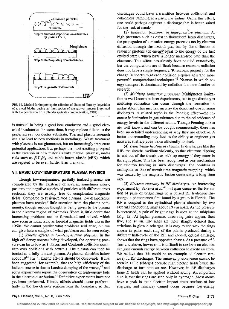
Thermal plasmas are a generic term for high-pressure plasmas that are so collisional that the particles and gases are in thermal equilibrium, though the radiation is, of course, not. Spray treatments of turbine blades and other airplane and automobile parts to harden the surfaces is already com- monplace. In fact, the manufacture of wire-arc sprays and other such equipment is a billion-dollar business. Unfortu- nately, not much of this money goes into research. The future lies not so much in the continued improvement of these de- vices but in finding new and exciting applications for them. For instance, diamond deposition is best done with thermal plasmas because of their high densities. Figure 13 shows such an apparatus. It has recently been found that the adhe- sion of a diamond coating can be strengthened by depositing a metal layer when the diamond crystals are half-grown, and then continuing to grow the crystals on top of the layer (Fig. 14). With a cheap method for diamond coatings, we can imagine that all cutting and sanding tools of the future will be so treated, and will hardly ever wear out. Since diamond
2172 Phys. Plasmas, Vol. 2, No. 6, June 1995 Francis F. Chen
Downloaded 27 Nov 2001 to 128.97.88.10. Redistribution subject to AIP license or copyright, see http://ojps.aip.org/pop/popcr.jsp
Diamond particles _-.
1 Substrate
Step 1: diamond deposition on substrates by plaSma CVD
Metal binder
Step 2: electroplating of metal binder
Step 3: re-growth of diamonds
FIG. 14. hletbod for improving the adhesion of diamond films by deposition of a metal binder during an interruption of the growth process [reprinted with the permission of E. Pfender (private communication, 1994)].
,..
is unusual in being a good heat conductor and a good elec- trical insulator at the same time, it may replace silicon as the preferred semiconductor substrate. Thermal plasma research can also lead to new methods in metallurgy. Waste treatment with plasmas is not glamorous, but an increasingly~important potential application. But perhaps the most exciting prospect is the creation of new materials with thermal plasmas, mate- rials such as p-CsN, and cubic boron nitride (cBN), which are reputed to be even harder than diamond.
VII. BASIC LOW-TEMPERATURE PLASMA PHYSICS
Though low-temperature, partially ionized plasmas are complicated by the existence of several, sometimes many, positive and negative species of particles with different cross sections, they are usually free ‘of complicated magnetic fields. Compared to fusion-related plasmas, low-temperature plasmas have received little attention from the plasma com- munity, though serious thought is being given to the plasma in the divertor region of tokamaks. There is little doubt that interesting problems can be formulated and solved, which now seem as intractable as toroidal magnetic fields did in the 1950s. We cannot predict what problems will arise, but we can give here a sample of what problems can be seen today.
(4) Transit-time heating in sheaths. In discharges like the RIE, the sheaths oscillate violently, so that electrons dipping in and out of the sheath can pick up energy if they enter in the right phase. This has been recognized as one mechanism for .electron heating in such discharges. The problem is analogous to that of transit-time magnetic pumping, which was treated by the magnetic fusion community a long time ago.
(1) Kinetic effects in low-temperature plasmas. In the high-efficiency sources being developed, the operating pres- sure can be as low as 1 mTorr, and Coulomb collisions domi- nate over collisions with neutrals. The plasma can then be treated as a fully ionized plasma. At plasma densities below about 1013 cmV3, kinetic effects should be observable. It has been suggested, for example, that the high efficiency of the helicon source is due to Landau damping of. the waves,” and some experiments report the observation of high-energy tails in the electron distribution.41 Definitive experiments have not yet been performed. Kinetic effects should occur preferen- tially in the low-density regions near the boundary, so that
(5) Elec&n runaway in RF discharges. An interesting experiment by Sakawa et a1.43 in Japan concerns the forma- tion of. pairs .of bright rings in a pulsed RF hydrogen dis- charge, a phenomenon first found by a group in Florida. The RF is coupled~ to the cylindric.al plasma chamber by two external conducting rings about 10 cm apart. As the pressure is increased,, a pair of bright rings is seen at the midplane (Fig. 15). At higher pressure, three ring pairs appear, then five, and, so on. The rings are more sharply defined than striations in glow discharges. It is easy to see why the rings appear in pairs: each ring of the pair is produced during a different half-cycle of the RF, and indeed, optical emission shows that the rings have *opposite phases. At a pressure of 3 Torr and above, however, it is difficult to see how an electron can gain enough energy between collisions to excite an atom. We believe that this could be an example of electron run- away in RF discharges. The runaway phenomenon cannot be seen in DC discharges because high electric fields cause the discharge to turn into an arc. However, in RF discharges large E fields can be applied without arcing. An important clue is that the rings are seen only in hydrogen. Most atoms have a peak in their electron impact cross sections at low energies, and runaway cannot occur because low-energy
Phys. Plasmas, Vol. 2, No. 6, June 1995 Francis F. Chen
discharges could have a transition between collisional and collionless damping at a particular radius. Using this effect, one could perhaps engineer a discharge that is better suited for the task at hand:: f
(2) Radiation transport in high-pre&re plasmas. At high pressures such as exist in fluorescent lamp discharges, the propagation of ionization energy proceeds not by.electron diffusion through the neutral gas, but by the diffusion of resonant photons (of-energf equal to the energy of the first excited state), which have a longer meanfree path than the electrons. This effect has already been studied extensively, but the computations are difficult because resonant radiation does not have a single frequency. To account properly for the change in Spectrumlat each collision requires new and more powerful computational techniques.4z Plasmas in which en- ergy transport is dominated by radiation is a new frontier of research. -
(3) Multistep iofzization processes. Multiphoton ioniza- tion is well known in laser experiments, but in gas discharges multistep ionization can occur through the formation of metastables. This mechanism may the dominant one in some discharges. A related topic. is the Penning effect-the in- crease in ionization in gas mixtures due to the coincidence of energy levels in the different atoms. Though Penning mixes are well known and can be bought commercially, there has been no detailed understanding of why they are effective. A better understanding may lead to the ability to engineer gas mixtures that are -even more efficiently ionized.
2173
Downloaded 27 Nov 2001 to 128.97.88.10. Redistribution subject to AIP license or copyright, see http://ojps.aip.org/pop/popcr.jsp

FIG. 15. Discrete ring pairs seen in a high-pressure RF discharge [reprinted with the permission of Y. Sakawa (Ref. 43)]. The number of pairs and their positions change with pressure, as shown in the graph.
electrons see a rising cross section as they gain energy. How- ever, hydrogen has a monotonically falling cross section (the cross section at low energy being enhanced by dipole inter- action), and could support runaway electrons. This is an ex- ample of a detailed experiment that needs a good theory.
(6) RF and microwave discharges for lighting. High- pressure discharges for the lighting industry is an area of research that is active, but not so active as to justify a sepa- rate section. The fluorescent lamp has a surprisingly high efficiency@ (65% conversion of electricity to UV) which probably cannot be further improved, but work is still being done to understand these discharges. At the same time, there is demand for new light sources based on microwave or RF excitation. For military applications, extremely bright and efficient lighting is needed for large areas, and for the home market the absence of internal electrodes may make a light bulb both long-lived and efficient. Though many inventions have been made, none, as yet, has been commercially suc- cessful that is not a variety of the fluorescent light.
(7) Effective use of instabilities. Normally, instabilities are undesirable, but in nonfusion applications one may actu- ally wish to excite instabilities. For instance, if one wanted to make an intense electron beam source out of a magnetized RF discharge, there would be no problem extracting the elec- trons, but ions would also have to be extracted in order to keep the plasma neutral. In that case, it would help to have an instability drive the ions out in another direction. Simi- larly, in the AVLIS scheme described below, an instability could be used to extract the ions more rapidly.
(8) Lsotope separation. The Plasma Separation Process is an isotope separation scheme based on selective cyclotron acceleration of ions of a certain mass. This process was in-
2174 Phys. Plasmas, Vol. 2, No. 6, June 1995 Francis F. Chen
vented by Dawson and developed by TRW, Inc.“’ Though the separation of uranium by this method is no longer funded, the process will work for any element. There is a need for medical isotopes produced this way. Discharges with differ- ent elements would have to be developed. Another isotope separation process is Atomic Vapor Laser Isotope Separation (AVLIS), which is based on selective ionization of one iso- tope by laser light.46 Once ionized, the separated ions must be driven out of the plasma and collected. To speed up the collection process, Japanese researchers have tried heating the electrons to increase the ion acoustic velocity and cyclo- tron heating the ions in a magnetic field. Thus, the problems are not laser problems, but real plasma problems.
VIII. CONCLUSION AND ACKNOWLEDGMENTS
In conclusion, we hope that these examples have given an idea of the excitement in the developing field of low- temperature plasma physics and of the opportunities for ap- plying to this field the techniques learned in studying high- temperature plasmas.
ACKNOWLEDGMENTS
We thank all the colleagues who lent their materials for this survey and apologize for any major misrepresentations that may have been made.
This work was supported by the National Science Foun- dation, the Wisconsin Engineering Research Center for Plasma-Aided Manufacturing, and the Liver-more Plasma Physics Research Institute.
‘J. W. Cobum and H. E Winters, J. Appl. Phys. SO, 3 189 (1979). 2J. W, Cobum, Plasma Etching and Reactive ion Etching, American Vacuum Society Monograph Series (American Institute of Physics, New York, 1982). p. 2.
3D. L. Flamm, in Plasma Etching, edited by D. M. Manos and D. L. Flamm (Academic, New York, 19891, p. 151.
4A. J. van Roosmaten, J. A. G. Baggerman, and S. J. H. Brader, Dry Etch- ing for VLSI (Plenum, New York, 1991), Chap. 6.
‘R. A. Gottscho, C. W. Jurgensen, and D. J. Vitkavage, J. Vat. Sci. Technol. B 10, 2133 (1992).
‘G. S. Selwyn, 3. E. Heidenreich, and K. L. Hailer, Appl. Phys. Lett. 57, 1876 (1990).
‘A. Garscadden. B. N. Ganguly, P. D. Haaland, and J. Williams, Plasma Sources Sci. Technol. 3, 239 (1994).
‘H. M. Anderson, S. Radovanov, J. L. Mock, and P J. Resnick, Plasma Sources Sci. Technol. 3,302 (1994).
9G. S. Selwyn, Plasma Sources Sci. Technol. 3, 340 (1994). “G. S. Selwyn (private communication, 1994). “S Fang and J. P McVittie, IEEE Electron. Devices Lett. ED-13,288, 347
(l.992). 12K. Nojiri and K. T. Tsunokuni, J. Vat, Sci. Technol. B 11, 1819 (1993). 13M. A. Lieberman and R. A. Gottscho, in Physics of Thin Films, edited by
M. Francomb and I. Vossen (Academic, New York, 19941, Vol. 18, pp. 1-119.
I40 A. Popov, in High Density Plasma Sources (Noyes, NJ, in press). tsJ.‘Asmussen, J. Vat. Sci. Technol. A 7, 883 (1989). 16J. P Hopwood, Plasma Sources Sci. Technol. 1, 109 (1992). “5. S. Ogle, US. Patent No. 4, 948, 458 (14 August 1990). “5 Hopwood, C. R. Guarnieri, S. J. Whitehair, and I. J. Cuomo, J. Vat. Sci.
Technol. A 11, 147, 152 (1993). 19F F Chen, “Helicon plasma sources,” in Ref. 14. “A. J. Perry and R. W. Boswell, Appl. Phys. Lett. 55, 148 (1989). “M. J. Hartig and M. I. Kushner, Appl. Phys. Lett. 62, 1594 (1993). 22V. Vabedi, C. K. Birdsall, M. A. Lieberman, G. DiPeso, and T. Rognlien,
Phys. Fluids B 5, 2719 (1993).
Downloaded 27 Nov 2001 to 128.97.88.10. Redistribution subject to AIP license or copyright, see http://ojps.aip.org/pop/popcr.jsp

asP. L. G. Ventzek, R. J. Hoekstra, M. J. Kushner, J. Vat. Sci. Technol. B 12, 461 (1994).
%G. diPeso, V. Vahedi, D. Hewett, and T. Rognlien, J. Vat. Sci. Technol. A 12, 1387 (1994).
ssR. A. Stewart, P. Vitello, and D. B.‘Graves, J. Vat. Sci. Technol. B 12,. 478 (1994).
*‘M. E. Barone and D. B. Graves, J. Appl. Phys. (in press). “J. A. Castellano, Handbook ofDisplay Technology (Academic, New York,
1992). %W. C. O’Mara, Liquid Crystal Flat Panel Displays (Van Nostrand Rein-
hold, New York, 1993). sgT. J. King, Xerox Corp. (private communication, 1994). 3oT. S. Buzak, SID’90 Digest (Society for Information Display, Santa Ana,
CA, 1990), p. 420. 311? S. Friedman, SID’93 Digest (Society for Information Display, Santa
Ana, CA, 1993), p. 176. s*S. Mikoshiba, Information Display 10, 21 (1994). 33D Peters, I. Paulus, and D. Stephani, J. Vat. Sci. Technol. B 12, 652
(l-994). % R. Conrad and K. Sridharan, in .I. Vat. Sci. Technol. B 12, 807 (1994).
35J. N. Matossian, J, Vat. Sci. Technol. B 12, 850 (1994). 36D. Rej, B. Wood, ‘R. Faehl, and H. Fleischmann, J. Vat. Sci. Technol. B
12, 861 (1994). 37D. Demon (private communication, 1994). 38R. d’ Agostino, Plasma Deposition, Treatment, und Etching of Polymers
(Academic, New York, 1990). 3gM. I: Boulos, P. Fauchais, and E. Pfender, Thermal Plasmas (Plenum, New
York, 1994). 40E F. Chen, Plasma Phys. Controlled Fusion 33, 339 (1991). 41P. Zhu and R. W. Boswell, Phys. Fluids B 3, 869 (1991). 42R. C. Wamsley, K. Mitsuhashi, and J. E. Lawler, Phys. Rev. E 47, 3540
(1993). 43Y. Sakawa, M. Hot? T Shoji, and T. Sato; “Evolution of paired luminous , .
rings in pulsed capacitive radio frequency discharges,” submitted to Phys. Rev. Lett.
44R. Piejak (private communication, 1994). 45F. E Chen, in From Fusion to Light Sufing, edited by T. Katsouleas
(Addison-Wesley, New York, 1991), p. 191. - 46K. Yamada, T. Tetsuka, and Y. Degucm, J. Appl. Phys. 67, 6734 (1990).
Phys. Plasmas, Vol. 2, No. 6, June 1995 Francis F. Chen 2175
Downloaded 27 Nov 2001 to 128.97.88.10. Redistribution subject to AIP license or copyright, see http://ojps.aip.org/pop/popcr.jsp