Indo-Spain Workshop Advances in Wafer Based Crystalline Si ... · being developed at IITB for point...
65
Advances in Wafer Based Crystalline Si Indo-Spain Workshop Advances in Wafer Based Crystalline Si cell Technology @ IITB Chetan S. Solanki March 2011 Department of Energy Science and Engineering Department of Energy Science and Engineering Indian Institute of Technology Bombay
Transcript of Indo-Spain Workshop Advances in Wafer Based Crystalline Si ... · being developed at IITB for point...

Advances in Wafer Based Crystalline SiIndo-Spain Workshop
Advances in Wafer Based Crystalline Sicell Technology @ IITB
Chetan S. Solanki
March 2011
Department of Energy Science and EngineeringDepartment of Energy Science and Engineering
Indian Institute of Technology Bombay

Acknowledgements Sastry A., Vinshu B., Vikrant C., Som M.,
Prof Anil, Dr. Meril

Contents Solar PV and India
National Center for Photovoltaic Research and Education (NCPRE)
Research directions on c-Si cells- Alternative metallization- Alternative metallization- Alternative junction- Alternative surface passivationp- Module cleaning solution
Summery
Chetan S Solanki, IIT Bombay 3
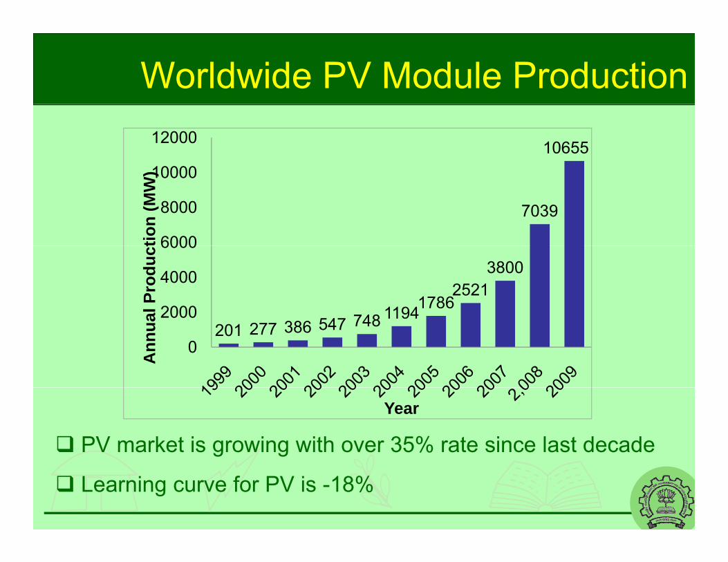
Worldwide PV Module Production
1065510000
12000)
7039
6000
8000
10000tio
n (M
W)
748 119417862521
3800
2000
4000
6000
al P
rodu
ct
201 277 386 547 748 1194
0
2000
Ann
ua
PV market is growing with over 35% rate since last decade
Year
Learning curve for PV is -18%
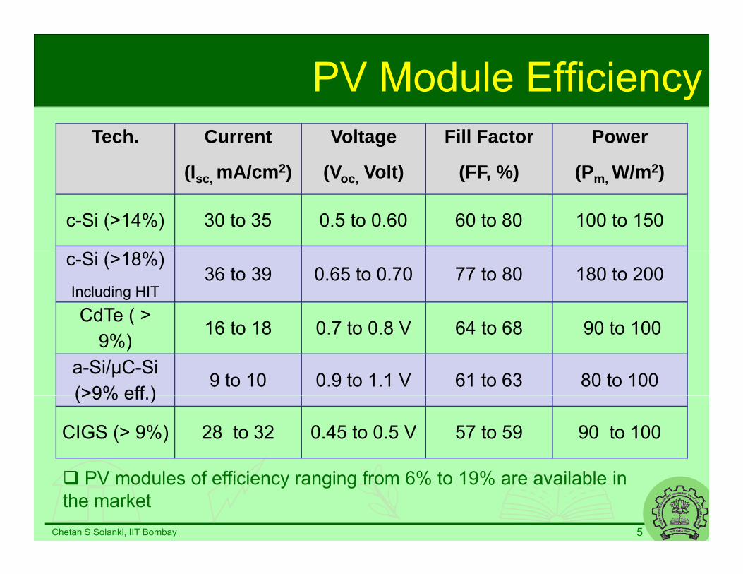
PV Module EfficiencyTech. Current
(Isc mA/cm2)
Voltage
(Voc Volt)
Fill Factor
(FF, %)
Power
(Pm W/m2)( sc, ) ( oc, ) ( , %) ( m, )
c-Si (>14%) 30 to 35 0.5 to 0.60 60 to 80 100 to 150
c-Si (>18%)
Including HIT36 to 39 0.65 to 0.70 77 to 80 180 to 200
CdTe ( > 16 t 18 0 7 t 0 8 V 64 t 68 90 t 100
(9%)
16 to 18 0.7 to 0.8 V 64 to 68 90 to 100
a-Si/µC-Si (>9% eff )
9 to 10 0.9 to 1.1 V 61 to 63 80 to 100(>9% eff.)
CIGS (> 9%) 28 to 32 0.45 to 0.5 V 57 to 59 90 to 100
Chetan S Solanki, IIT Bombay 5
PV modules of efficiency ranging from 6% to 19% are available in the market
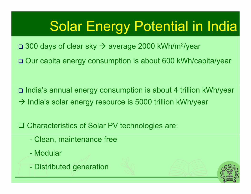
Solar Energy Potential in India 300 days of clear sky average 2000 kWh/m2/year
Our capita energy consumption is about 600 kWh/capita/year Our capita energy consumption is about 600 kWh/capita/year
India’s annual energy consumption is about 4 trillion kWh/year India’s solar energy resource is 5000 trillion kWh/year
Characteristics of Solar PV technologies are:
- Clean, maintenance free
- Modular
- Distributed generation
Solar PV in IndiaCurrent cell and module manufacturing capacity is about 400 and 750 MWp respectively
Jawaharlal Nehru National Solar Mission (JNNSM) has been announced to promote solar PV electricity generation in Indiaannounced to promote solar PV electricity generation in India
SIPS scheme for promoting solar PV manufacturing in India
Target is to install 20,000 MW of Solar power in India by 2022 stirred lot of activities in the country
The Mission document mentions NCPRE at IIT Bombay:“setting up of a National Centre for Photovoltaic Research & Education
Chetan S Solanki, IIT Bombay 7
at IIT Bombay, drawing upon its Department of Energy Science & Engineering and its Centre of Excellence in Nanoelectronics”

National Centre for Photovoltaic Research & Education (NCPRE)( )
• IIT Bombay’s activities in Energy, Semiconductors, Materials and Power Electronics will converge together in NCPRE
• NCPRE will be the country’s major academic centre to support the photovoltaics (PV) part of the Jawaharlal Nehru National Solar Mission
• NCPRE has started functioning in October 2010, with a funding from the Government of Rs. 47.5 crore for 5 years
• NCPRE will be highly interdisciplinary, drawing upon the expertise of g y p y, g p p51 faculty members from 13 Departments at IIT Bombay
• NCPRE will cover many aspects of PV, including solar cells, new materials, power electronics, grid connection, rural deployment and p g p ypolicy issues
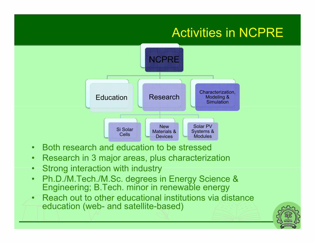
Activities in NCPRE
NCPRE
Education ResearchCharacterization,
Modeling & Simulation
Si Solar Cells
New Materials &
Devices
Solar PV Systems & Modules
• Both research and education to be stressed• Research in 3 major areas, plus characterization• Strong interaction with industry
Devices Modules
• Strong interaction with industry• Ph.D./M.Tech./M.Sc. degrees in Energy Science &
Engineering; B.Tech. minor in renewable energy• Reach out to other educational institutions via distance• Reach out to other educational institutions via distance
education (web- and satellite-based)

Facilities for NCPRE• Excellent facilities already exist at IIT Bombay for silicon
fabrication, power electronics and solar cells:
Furnaces Implantater RTP Anneal Solar Cell TesterHWCVD
St t f th t f iliti ill b t th h thGate Stack Tool Solar Modules Power Electronics
• State-of-the-art new facilities will be set up through the funding of NCPRE

Education & Training- @ NCPRE Programmes at IITB Ph.D. M.Tech. M.Sc. B.Tech. Minor programme at UG level
Preparation of Course Material Preparation of Course Material Course Modules Laboratory Kits Teacher Training Programmes Training “Master Technicians”Training Master Technicians
Distance Education Web- and Satellite-based Post-Graduate Diploma for working professionals
Training programmes for Industry Short-term courses Certificate programmes Post Graduate Diploma for working professionals Post-Graduate Diploma for working professionals
Indian National Photovoltaics Users’ Programme (as a separate project)
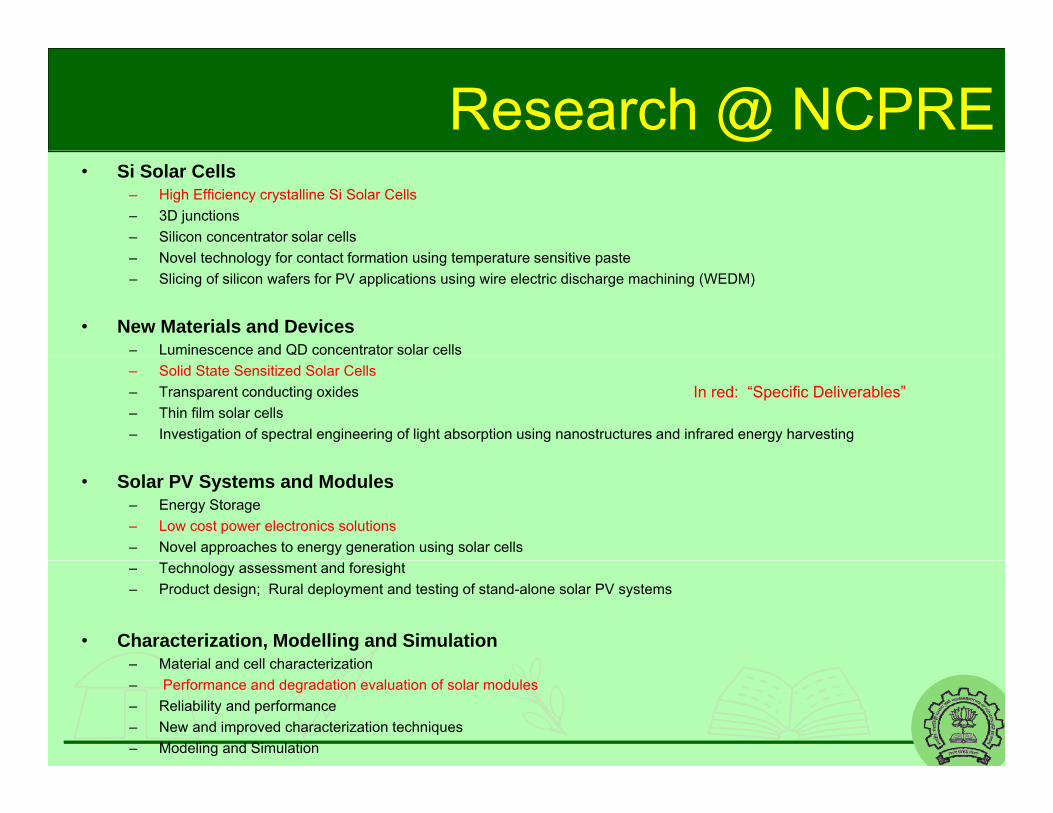
Research @ NCPRE• Si Solar Cells
– High Efficiency crystalline Si Solar Cells– 3D junctions– Silicon concentrator solar cells
N l t h l f t t f ti i t t iti t– Novel technology for contact formation using temperature sensitive paste– Slicing of silicon wafers for PV applications using wire electric discharge machining (WEDM)
• New Materials and Devices– Luminescence and QD concentrator solar cells– Solid State Sensitized Solar Cells– Transparent conducting oxides– Thin film solar cells– Investigation of spectral engineering of light absorption using nanostructures and infrared energy harvesting
In red: “Specific Deliverables”
• Solar PV Systems and Modules– Energy Storage– Low cost power electronics solutions– Novel approaches to energy generation using solar cells – Technology assessment and foresight– Product design; Rural deployment and testing of stand-alone solar PV systems
• Characterization, Modelling and SimulationMaterial and cell characterization– Material and cell characterization
– Performance and degradation evaluation of solar modules– Reliability and performance– New and improved characterization techniques– Modeling and Simulation

Research on C-Si Solar Cells
Chetan S Solanki, IIT Bombay 13

Technology gaps: Laboratory vs Industrial
Ideal Example of Si
Ref: L.L. Kazmerski / Journal of Electron Spectroscopy and Related Phenomena 150 (2006) 105–135.
Ideal
Best lab
Best com. cells
Typical Typical com.
module
Large “W/m2” is important high efficiency is important
Chetan S Solanki, IIT Bombay 14
g p g y p
All laboratory processes are not commercially vaible
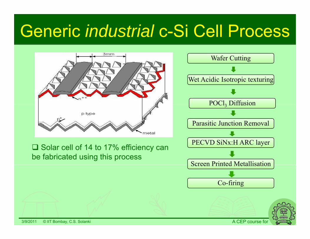
Generic industrial c-Si Cell ProcessWafer Cutting
Standard processWet Acidic Isotropic texturing
POCl3 DiffusionPOCl3 Diffusion
Parasitic Junction Removal
PECVD SiNx:H ARC layer
Screen Printed Metallisation
Solar cell of 14 to 17% efficiency can be fabricated using this process
Co-firing
Screen Printed Metallisation
3/9/2011 © IIT Bombay, C.S. Solanki A CEP course for 15
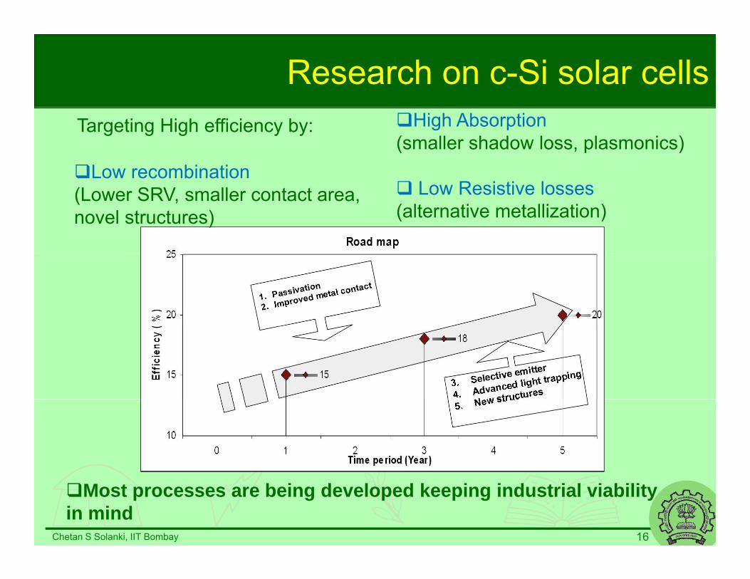
Research on c-Si solar cellsHigh Absorption (smaller shadow loss, plasmonics)
Low recombination
Targeting High efficiency by:
Low Resistive losses(alternative metallization)
(Lower SRV, smaller contact area, novel structures)
Chetan S Solanki, IIT Bombay 16
Most processes are being developed keeping industrial viability in mind

Towards 18% cellBasic cell processes are being developed and optimized
Silicon Nitride
Front contact(Ti/Pd/Ag)
P-type Substrate
N-type emitter (Phosphorus doped)
B k C t t (Al)yp
Back Contact (Al)
Chetan S Solanki, IIT Bombay 17

Approach for 20% cell18% cell. PC1D Simulation Parameters
Total series resistance = 0 01Ω
Reduction in SRV from 105
cm/s to few 100 cm/s can enhance current by about 3 Total series resistance 0.01Ω
Shunt conductance = 0.002Sτn = 100 μs, τp = 50 μsFront surface: Sn = Sp = 105 cm/s
ymA/cm2 and voltage by about 30 mV
Selective metal contact ispJunction Depth = 0.3 μmJsc = 36 mA/cm2
Voc = 0.640 V
Selective metal contact is being developed at IITB for point contact, selective emitter and electroplated contacts
FF = 78%p
2 to 3 % absolute enhancement in efficiency is obtainable Overall more thanobtainable Overall more than 20%
Chetan S Solanki, IIT Bombay 18
Ref: Bernhard V. et al, C-Si solar cells, John Wiley and Sons, 1998.

Alternative MetallizationMetal contact patterningMetal contact patterning
Metal contact deposition
Chetan S Solanki, IIT Bombay 19
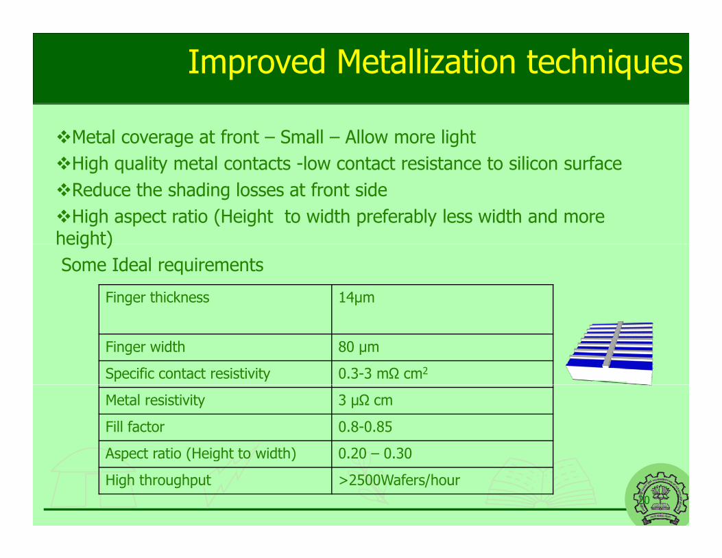
Improved Metallization techniques
Metal coverage at front – Small – Allow more light High quality metal contacts -low contact resistance to silicon surfaceReduce the shading losses at front sideHigh aspect ratio (Height to width preferably less width and more height)height)Some Ideal requirements
Finger thickness 14µm
Finger width 80 µm
Specific contact resistivity 0.3-3 mΩ cm2
Metal resistivity 3 µΩ cm
Fill factor 0.8-0.85
Aspect ratio (Height to width) 0 20 – 0 30
20
Aspect ratio (Height to width) 0.20 0.30
High throughput >2500Wafers/hour
Metallization techniques
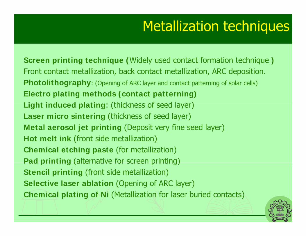
Screen printing technique (Widely used contact formation technique )Front contact metallization, back contact metallization, ARC deposition.Front contact metallization, back contact metallization, ARC deposition.Photolithography: (Opening of ARC layer and contact patterning of solar cells)
Electro plating methods (contact patterning)Li ht i d d l ti (thi k f d l )Light induced plating: (thickness of seed layer)Laser micro sintering (thickness of seed layer)Metal aerosol jet printing (Deposit very fine seed layer)Hot melt ink (front side metallization)Chemical etching paste (for metallization)Pad printing (alternative for screen printing)Pad printing (alternative for screen printing)Stencil printing (front side metallization)Selective laser ablation (Opening of ARC layer)Ch i l l ti f Ni (M t lli ti f l b i d t t )Chemical plating of Ni (Metallization for laser buried contacts)

ARC Patterning for plated contactsOpening of ARC coatings:
U i h i l t hi ARC ( ll ARC thi k i b t 0 05Using chemical etching, ARC (generally ARC thickness is about 0.05 –1.54 µm) can be removed selectively.For example: HF, H3PO4.
Metallization can be done after opening of the ARC coatings using Ni/Cu process.
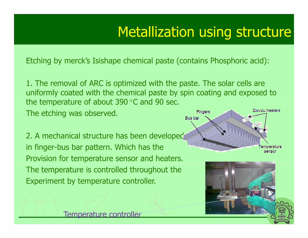
Metallization using structure
Etching by merck’s Isishape chemical paste (contains Phosphoric acid):
1. The removal of ARC is optimized with the paste. The solar cells are uniformly coated with the chemical paste by spin coating and exposed to the temperature of about 390C and 90 sec.the temperature of about 390 C and 90 sec.The etching was observed.
2 A h i l t t h b d l d2. A mechanical structure has been developed in finger-bus bar pattern. Which has the Provision for temperature sensor and heaters.The temperature is controlled throughout the Experiment by temperature controller.
23Temperature controller
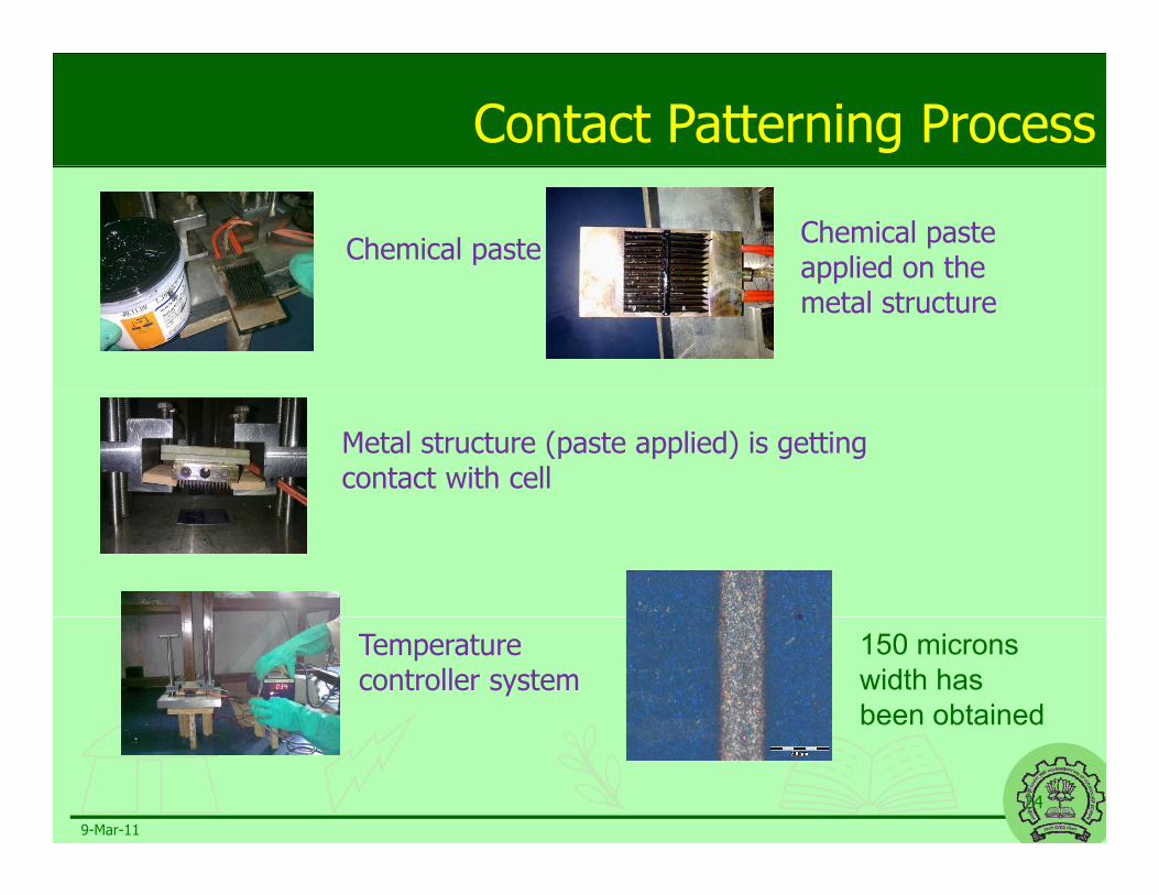
Contact Patterning Process
Chemical paste Chemical paste applied on the ppmetal structure
Metal structure (paste applied) is getting contact with cell
Temperature controller system
150 microns width has been obtained
9-Mar-11
24
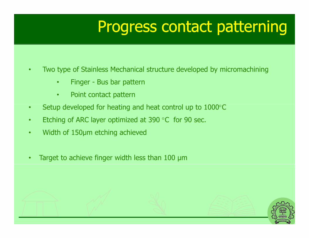
Progress contact patterningProgress contact patterning
• Two type of Stainless Mechanical structure developed by micromachining
• Finger - Bus bar pattern
• Point contact pattern
• Setup developed for heating and heat control up to 1000C
• Etching of ARC layer optimized at 390 C for 90 sec.
• Width of 150µm etching achievedWidth of 150µm etching achieved
• Target to achieve finger width less than 100 µm

Ni/Cu two step metallization for c-Si solar cells
Chetan S Solanki, IIT Bombay 26

Two step metallization to reduce the series resistance of the solar cell
• High series resistance of the commercial c-Si solar cells• Due to the higher resistance of screen printed grid lines and also
higher contact resistivityhigher contact resistivity• Electro-deposition is one of the possible answer to reduce the
resistance of the grid lines• Use of Silicide (NiSi) to reduce the contact resistivity between the( ) y
metal-semiconductor contact (silicide is confirmed using XRD aXPS analysis)
• Two step metalization of electro-deposited contacts to reduce thegrid lines resistance and the contact resistivity
• Ni/Cu are two suitable choices, due to their low cost, easy availability and ease of processing
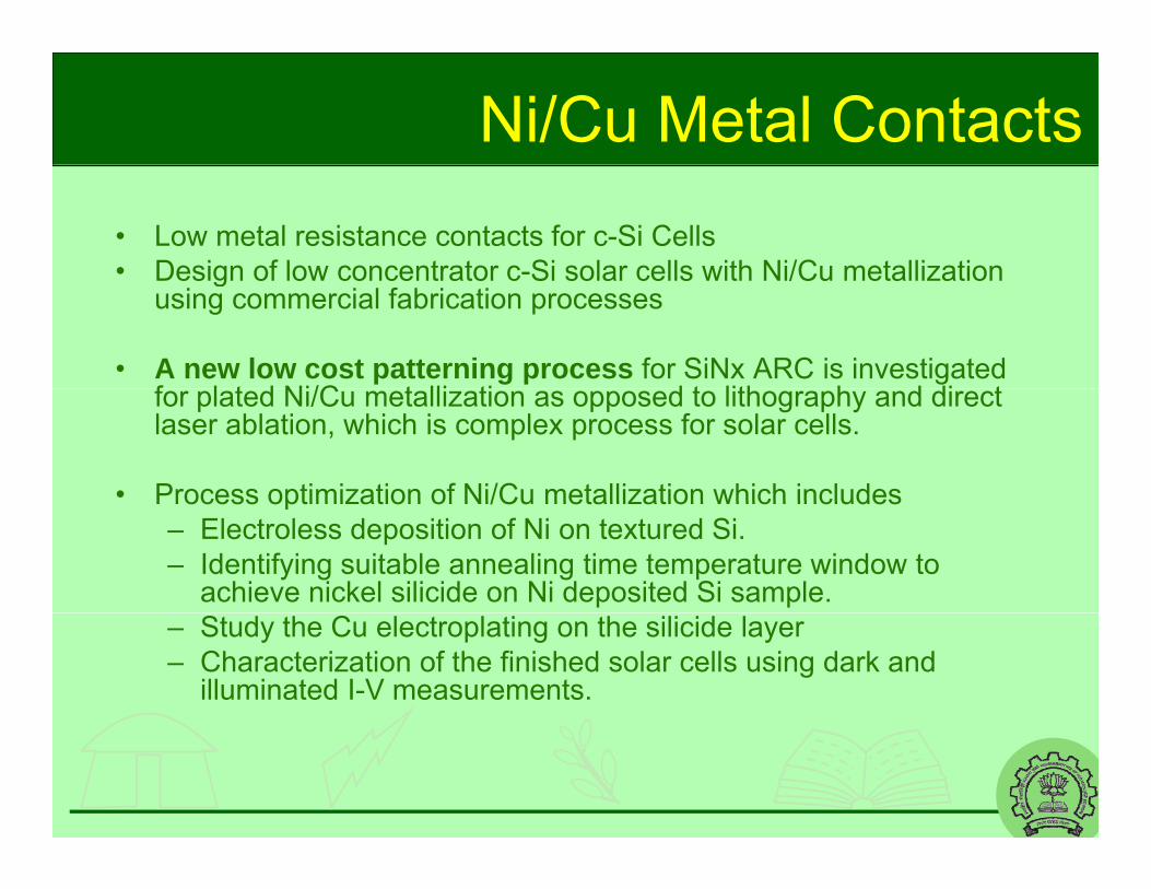
Ni/Cu Metal Contacts• Low metal resistance contacts for c-Si Cells• Design of low concentrator c-Si solar cells with Ni/Cu metallizationDesign of low concentrator c Si solar cells with Ni/Cu metallization
using commercial fabrication processes
• A new low cost patterning process for SiNx ARC is investigated f l t d Ni/C t lli ti d t lith h d di tfor plated Ni/Cu metallization as opposed to lithography and direct laser ablation, which is complex process for solar cells.
• Process optimization of Ni/Cu metallization which includesProcess optimization of Ni/Cu metallization which includes – Electroless deposition of Ni on textured Si. – Identifying suitable annealing time temperature window to
achieve nickel silicide on Ni deposited Si sample. – Study the Cu electroplating on the silicide layer – Characterization of the finished solar cells using dark and
illuminated I-V measurements.
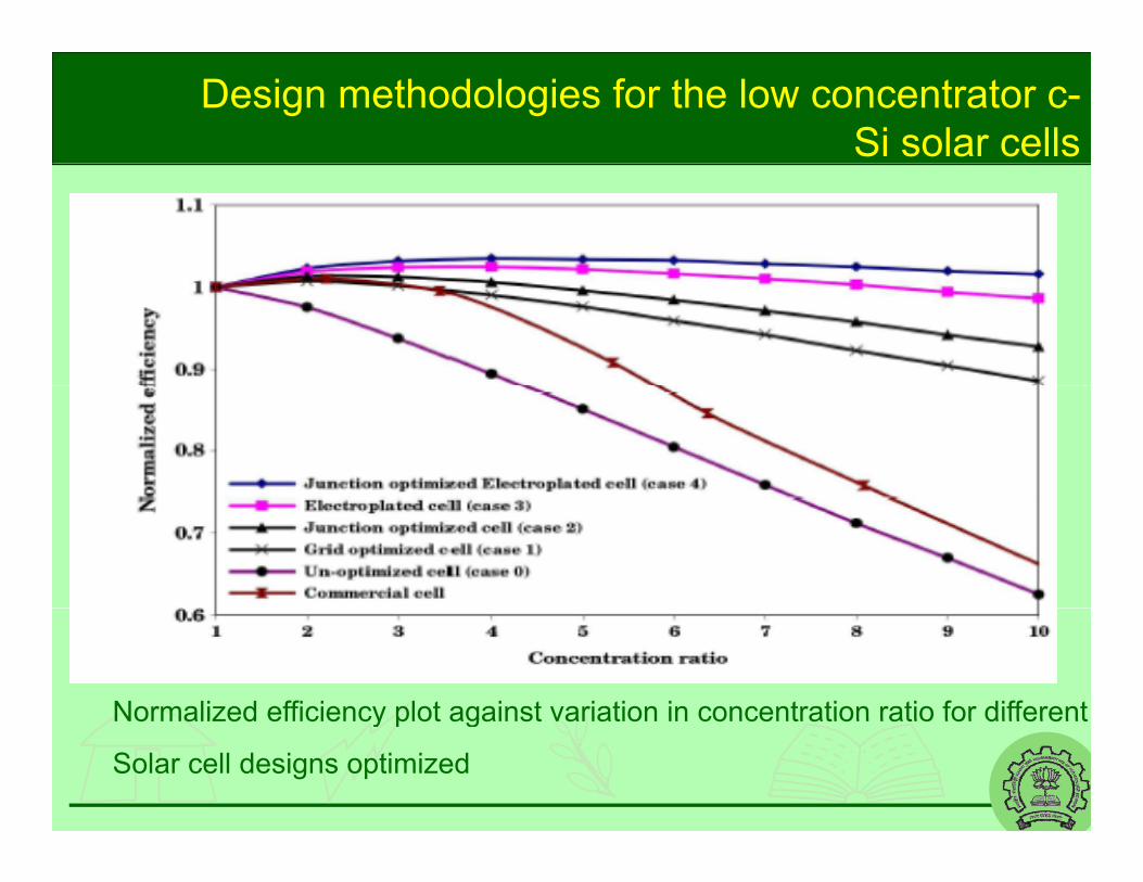
Design methodologies for the low concentrator c-Si solar cells
Normalized efficiency plot against variation in concentration ratio for differentNormalized efficiency plot against variation in concentration ratio for different
Solar cell designs optimized

Results of optimization study
Optimization procedure used forthe design of the solar cell
Relative change in efficiency from 1sun obtained for solar celloperating at 10 sun
Junction optimized electroplated solarcell
+2-3 %
Electroplated grid optimized solar cell -1 %
Junction and grid optimized solar cell -5 %
Grid optimized solar cell -10 %
Unoptimized solar cell -35 %Unoptimized solar cell 35 %
Commercial solar cell(experimental estimated value)
-30%

NiSi as a contacting material for solar cells
Contact resistivity of NiSi contacts on solar cells and comparison with screen printed contacts

Process steps for two step metallization

Deposition conditions of Ni/Cu
• The electroless Nickel plating on the N-type Si wafers with resistivity in the range of 0.1- 0.6 and sheet resistance in the range of 6.5-7.5 Ω/ has been done.S l d C f BATH COMPOSITION f l t l Ni• Selected Components for BATH COMPOSITION for electroless Ni-plating
1. Nickel chloride hexahydrate (NiCl2.6H2O, 30g/l) as a basic source of metal2 Sodium hypophosphite monohydrate (NaH PO H O 20g/l) as a reducing2. Sodium hypophosphite monohydrate (NaH2PO2.H2O, 20g/l) as a reducing
agent3. Ammonium chloride (NH4Cl, 50g/l) as buffering agent for stability of solution
for long time.4. Triammonium citrate (C6H17N3O7, 65g/l) as the complexing agent.• Here traditional sensitization by stannous chloride (SnCl2.2H2O, 50g/l) and
activation by palladium chloride (PdCl2) has been applied.
• Selected Components for BATH COMPOSITION for Cu-electroplating
1. Cupric sulphate (CuSO4.5H2O, 40g/l) as a basic source of metal1. Cupric sulphate (CuSO4.5H2O, 40g/l) as a basic source of metal2. H2SO4, 25 ml/l
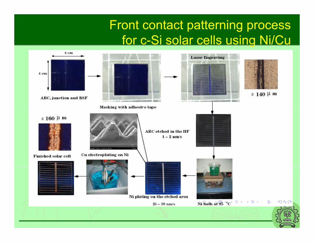
Front contact patterning processfor c-Si solar cells using Ni/Cug
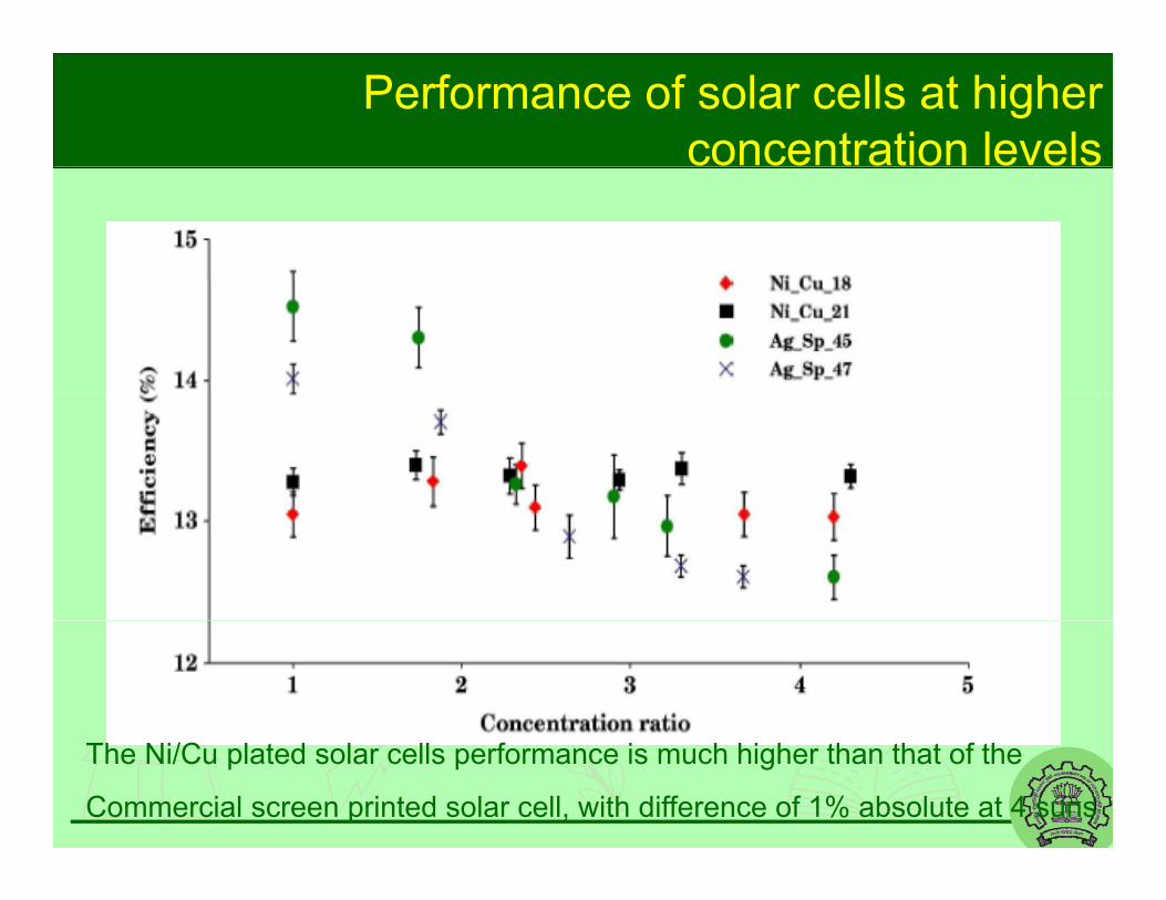
Performance of solar cells at higher concentration levels
The Ni/Cu plated solar cells performance is much higher than that of the
Commercial screen printed solar cell, with difference of 1% absolute at 4 suns
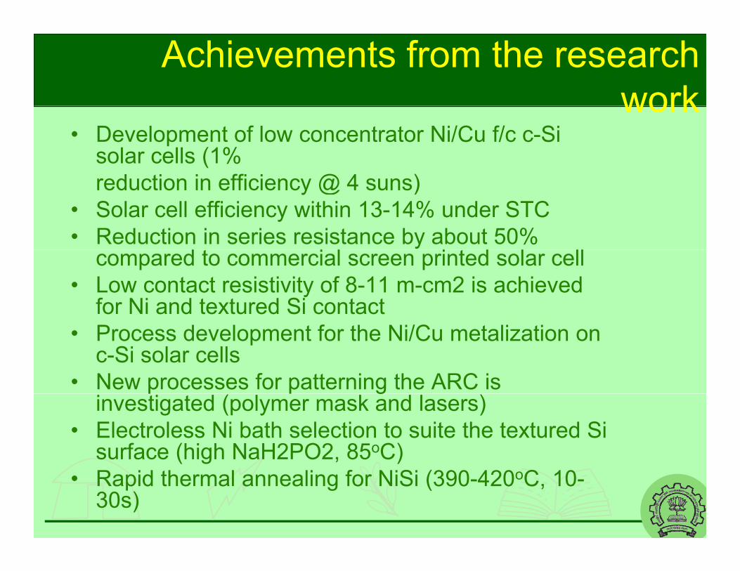
Achievements from the research workwork
• Development of low concentrator Ni/Cu f/c c-Si solar cells (1%
d ti i ffi i @ 4 )reduction in efficiency @ 4 suns)• Solar cell efficiency within 13-14% under STC• Reduction in series resistance by about 50%
d i l i d l llcompared to commercial screen printed solar cell• Low contact resistivity of 8-11 m-cm2 is achieved
for Ni and textured Si contact• Process development for the Ni/Cu metalization on
c-Si solar cells• New processes for patterning the ARC is p p g
investigated (polymer mask and lasers)• Electroless Ni bath selection to suite the textured Si
surface (high NaH2PO2, 85oC)• Rapid thermal annealing for NiSi (390-420oC, 10-
30s)

Adhesion: A problem
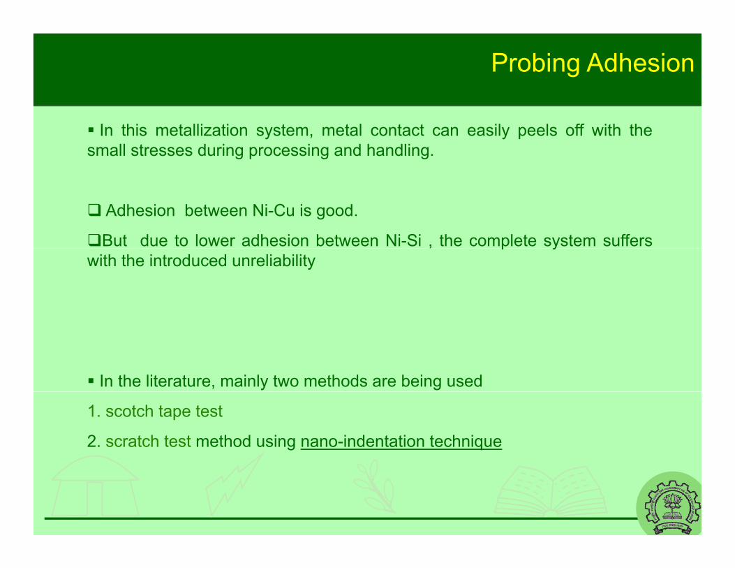
Probing Adhesion
In this metallization system, metal contact can easily peels off with thesmall stresses during processing and handling.
Adhesion between Ni-Cu is good.
But due to lower adhesion between Ni-Si , the complete system suffers, p ywith the introduced unreliability
In the literature, mainly two methods are being used
1. scotch tape test
2. scratch test method using nano-indentation technique
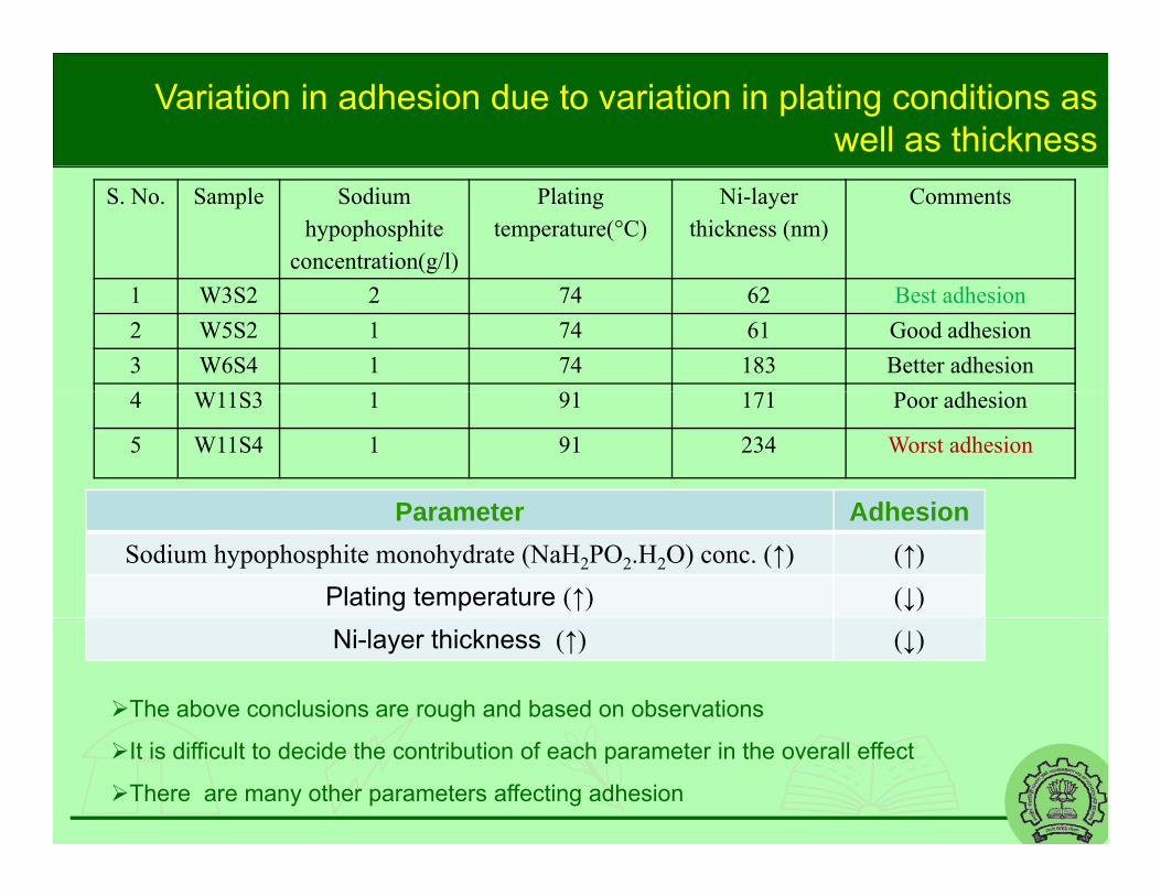
Variation in adhesion due to variation in plating conditions as well as thickness
S. No. Sample Sodium hypophosphite
concentration(g/l)
Plating temperature(°C)
Ni-layer thickness (nm)
Comments
1 W3S2 2 74 62 Best adhesion2 W5S2 1 74 61 Good adhesion3 W6S4 1 74 183 Better adhesion
dh i4 W11S3 1 91 171 Poor adhesion
5 W11S4 1 91 234 Worst adhesion
P t Adh iParameter AdhesionSodium hypophosphite monohydrate (NaH2PO2.H2O) conc. (↑) (↑)
Plating temperature (↑) (↓)Ni-layer thickness (↑) (↓)
The above conclusions are rough and based on observations
It is difficult to decide the contribution of each parameter in the overall effect
There are many other parameters affecting adhesion
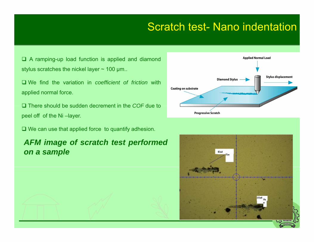
Scratch test- Nano indentation
A ramping-up load function is applied and diamond
stylus scratches the nickel layer ~ 100 μm..
We find the variation in coefficient of friction with
applied normal force.
There should be sudden decrement in the COF due to There should be sudden decrement in the COF due to
peel off of the Ni –layer.
We can use that applied force to quantify adhesion.
AFM image of scratch test performedon a sample
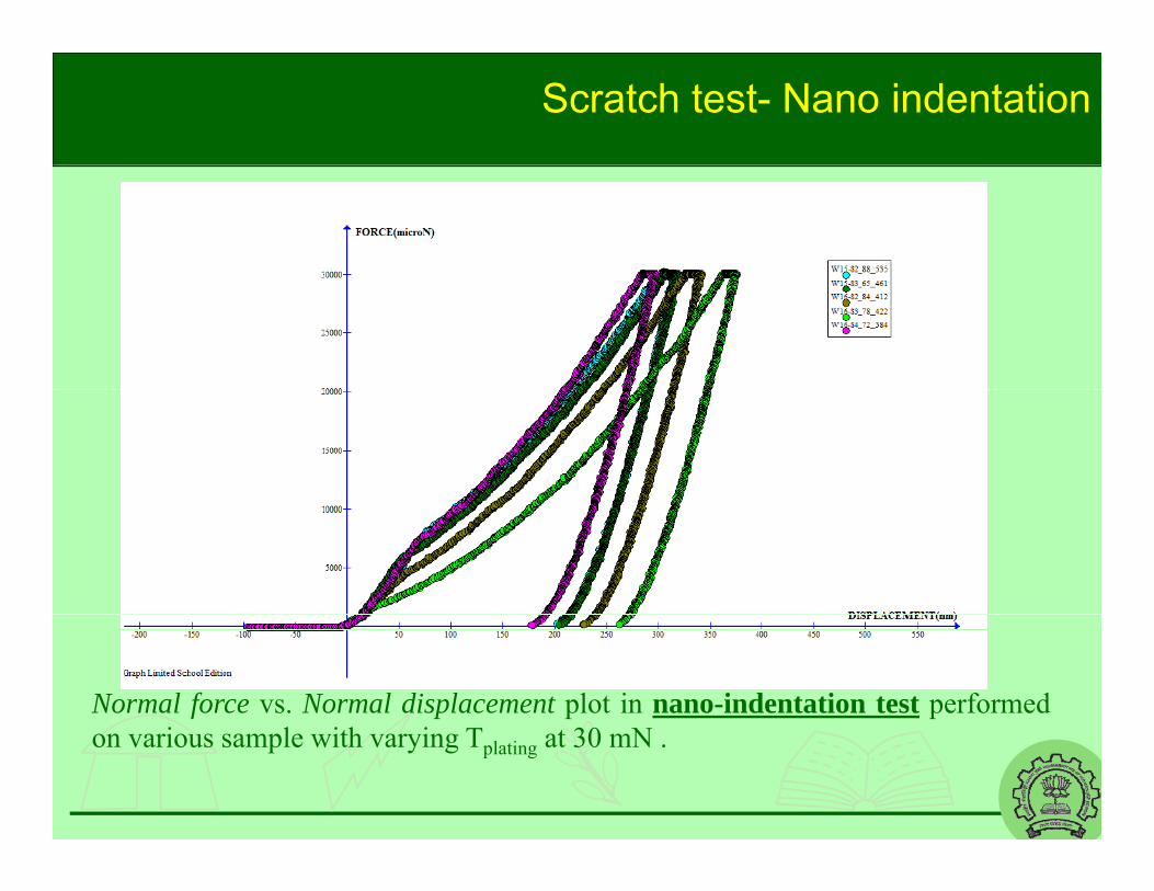
Scratch test- Nano indentation
Normal force vs. Normal displacement plot in nano-indentation test performedon various sample with varying Tplating at 30 mN .

Alternative Junction
Chetan S Solanki, IIT Bombay 31st May-09 42

3D Junction solar cells3D junction as compared to planner junction in conventional cells
Better carrier collection , carriers are generated close to junction
Suitable for low lifetime c SiSuitable for low lifetime c-Si materials, like solar grade Si
Smaller shadow losses –as low as 0-3 % compared to 7-8% in conventional cells
Theoretical and Experimental
43
pstudies are in progress
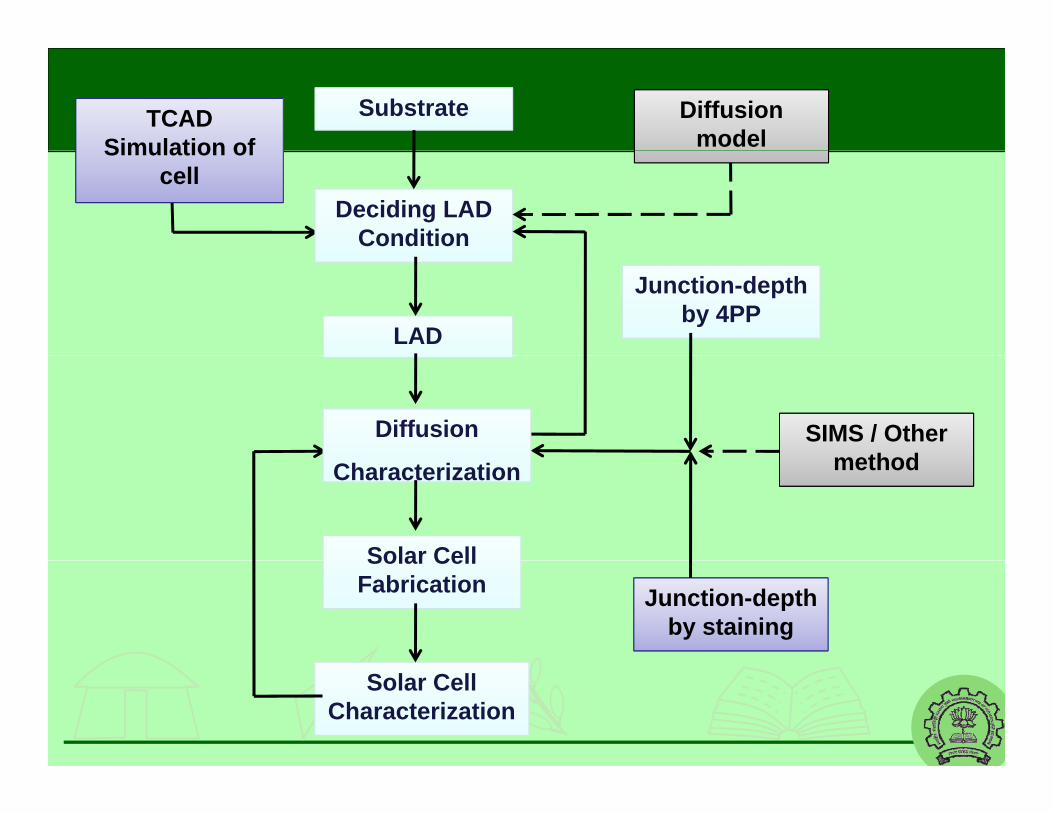
Substrate Diffusion model
TCAD Simulation of
Deciding LAD Condition
Simulation of cell
LAD
Junction-depth by 4PP
SIMS / Other method
Diffusion
Solar Cell
methodCharacterization
Solar Cell Fabrication Junction-depth
by staining
Solar Cell Characterization
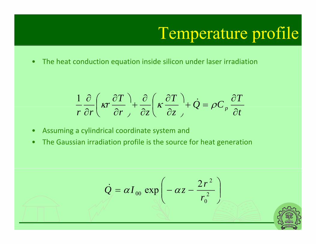
Temperature profile • The heat conduction equation inside silicon under laser irradiation
TCQTTr
1
• Assuming a cylindrical coordinate system and
tCQ
zzrr
rr p
• The Gaussian irradiation profile is the source for heat generation
2
2
002exprrzIQ
0r

Temperature profile • The boundary conditions assumed for this problem is
(i) at r = 0, 0
rT
(ii) at , T=Tar
(iii) & (iv) at z = 0 & z = L ,
44 TTTThT
• And the initial condition is
(v) at t 0 T 300
TTTThz ac
(v) at t = 0, T = 300
Temperature profile - Solution
• Solved using numerical method
V i i f h l d i i d h l diff i i i h• Variation of thermal conductivity and thermal diffusivity with temperature
• 3‐D transient state3 D transient state
• Finite difference method applied
• Explicit method
• Calculation of temperature rise after 1 ns during the pulse irradiation

Experimental – Jn-depth measurement
Etch solution HF:HNO3 = 1:100 Measured voltage with 10 mA current 10 s etch stepsp 3-5 nm/s etch rate Not verified with SIMS data
48

Contd. 6
8
)
4
6
Volta
ge (V
)0
2
0 5 10 15 20Vo
0 5 10 15 20Steps
Emitter sheet i t ( h / )
Junction depth with correction factor (nm)resistance (ohms/sq.)
p ( )
50 – 60709595
40 – 50 221210176176
15 – 20 410 49
P-type c-silicon surface passivation using sputtered
aluminum oxide(AlAl22OO33)
Chetan S Solanki, IIT Bombay 50

Background
• It is difficult to find a suitable passivation layer for p‐type c‐Si surfaces as most available oxide layers contains positive charges.y p g
•• AlAl22OO3 3 is known to contain a lot of negative charges irrespective of the deposition technique.
• ALD deposited AlAl22OO33 layer contains negative charges ~5‐6X 10¹²ALD deposited AlAl22OO3 3 layer contains negative charges 5 6X 10
/ cm² and comparatively less interface charges ~ 10¹¹ /eV‐cm²
• As deposited AlAl22OO33 layers do not passivates the c‐Si layers much but it passivates the c Si layer effectively after annealing in the temperature ~4250Cpassivates the c‐Si layer effectively after annealing in the temperature 4250C
• Surface recombination velocity < 10 cm/sec has been achieved for c‐Si surfaces with ALD AlAl22OO3 3 layers.

Properties of Al2O3
• Al2O3 has a very large bandgap of ~8.8 eVAl2O3 has a very large bandgap of 8.8 eV for crystalline Al2O3.
• The Al2O3 film is therefore transparent for the wavelength region which is relevant for t e a e e gt eg o c s e e a t osilicon solar cell (400‐1100 nm).
• Optical band gap of 6.4± 0.1 eV was experimentally calculated for ALD a‐Al2O3 p yfilm, is still large.
• The refractive index of Al2O3 was ~1.65 i.e slightly greater than that SiO2 (1.46).g y g ( )
G.Dingemans and W.M.M. Kessels, “Proceedings of the 25th European Photovoltaic Solar Energy Conference, Valencia, Spain(2010)”
Properties of Al2O3
• Firing process dose not activate the Al2O3 surface passivation. However, deposition of SiN capping layer on Al2O3 activates the surface passivation. SiN capping does not increase the good thermal stability of Al2O3 passivation.
• Al2O3 layer has negative charges, therefore produces an accumulation layer at the rear Si surface. Hence not suffered from parasitic shunting effect as it is in the case of SiN X.
• The interface defect density of c‐Si/Al2O3 system was found unaffected by ultraviolet radiation.
• The negative fixed charge density in Al2O3 was found to be increased on exposure to UV light due to photon induced electron injection.
Al2O3 by sputtering
Experiment:
• Applied Materials Endura system(PVD sputtering) is used to deposit Al2O3 layer on p‐type c‐Si (1‐5 ohm‐cm, <100>, cz).
• The characteristics of the deposited Al2O3 layers are changed with p 2 3 y gvariation in oxygen and argon flow rates and RF power.
• Al2O3 layers are deposited in 5‐ steps
• RCA is carried out on all the wafers and 2% HF deposition justRCA is carried out on all the wafers and 2% HF deposition just before the Al2O3 deposition.
• Aluminum is used for both front and back contacts and deposited using Evaporationusing Evaporation.
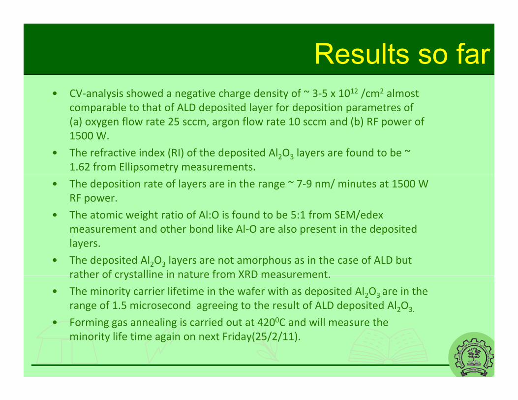
Results so far• CV‐analysis showed a negative charge density of ~ 3‐5 x 10¹² /cm2 almost
comparable to that of ALD deposited layer for deposition parametres of (a) oxygen flow rate 25 sccm, argon flow rate 10 sccm and (b) RF power of(a) oxygen flow rate 25 sccm, argon flow rate 10 sccm and (b) RF power of 1500 W.
• The refractive index (RI) of the deposited Al2O3 layers are found to be ~ 1.62 from Ellipsometry measurements.
• The deposition rate of layers are in the range ~ 7‐9 nm/ minutes at 1500 W RF power.
• The atomic weight ratio of Al:O is found to be 5:1 from SEM/edexd h b d lik Al O l i h d i dmeasurement and other bond like Al‐O are also present in the deposited
layers.
• The deposited Al2O3 layers are not amorphous as in the case of ALD but rather of crystalline in nature from XRD measurementrather of crystalline in nature from XRD measurement.
• The minority carrier lifetime in the wafer with as deposited Al2O3 are in the range of 1.5 microsecond agreeing to the result of ALD deposited Al2O3.
• Forming gas annealing is carried out at 4200C and will measure the g g gminority life time again on next Friday(25/2/11).
Surface Plasmons for Enhanced Absorption
Chetan S Solanki, IIT Bombay 56
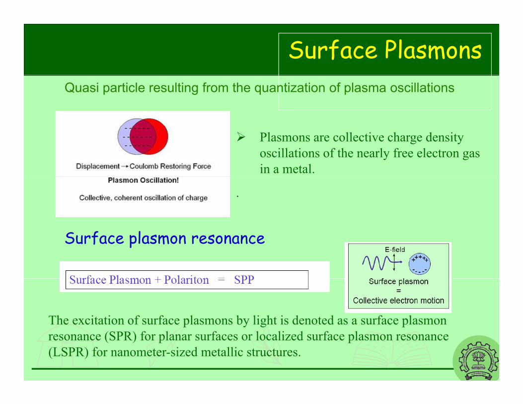
Surface PlasmonsQuasi particle resulting from the quantization of plasma oscillations
Plasmons are collective charge density oscillations of the nearly free electron gas in a metal.
.
Surface plasmon resonance
The excitation of surface plasmons by light is denoted as a surface plasmon resonance (SPR) for planar surfaces or localized surface plasmon resonance (LSPR) for nanometer-sized metallic structures.

Conventional Silicon solar cells
•Thick absorption layers (wafers) due to indirect bandgap Plasmonics
Thin film solar cells
•High quality wafers to ensure carrier life time of thick layers
Metals nano particles
•Thinner cells to compromise low carrier diffusion length due
we need thinner wafers and methods to increase absorption enhancement in thinner wafers +
Metals nano particles enable efficient
incorporation of light
Thinner cells to compromise low carrier diffusion length due to high defect density
•Thinner cells reduce the amount of light absorbed
Thi fil l llIncrease the absorption of thinner films
Thin film solar cells
•Low efficiency
Exciting New Opportunity!
Combining the field of Plasmonics and photovoltaics
•Low cost
To improve the efficiency

360 Sun tracking system with g yAutomatic Cleaning System for Solar
PV module
Chetan S Solanki, IIT Bombay 59
Effect of dust on PV modules
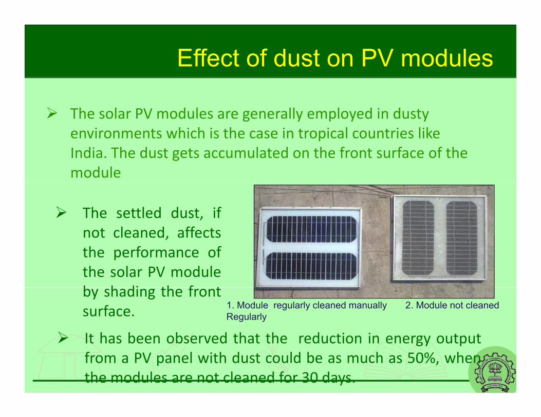
The solar PV modules are generally employed in dusty i t hi h i th i t i l t i likenvironments which is the case in tropical countries like
India. The dust gets accumulated on the front surface of the module
The settled dust, ifnot cleaned affectsnot cleaned, affectsthe performance ofthe solar PV moduleb h di th f t
1. Module regularly cleaned manually 2. Module not cleaned Regularly
by shading the frontsurface.
It has been observed that the reduction in energy output It has been observed that the reduction in energy outputfrom a PV panel with dust could be as much as 50%, whenthe modules are not cleaned for 30 days.

360 degrees tracking cum cleaning
Sun tracking cum cleaning mechanism for Solar PV module is
l i d i hexplained in the two steps (A and B) mentioned below:
A. Tracking mechanism A single axis tracking of the
solar PV module is done alongsolar PV module is done along with the automated cleaning mechanism.
The module is rotated 360 degrees in 24 hours.
The module starts its rotation from vertical position at the time of sunrise facing east (perpendicular to ground) and rotates at the rate of 15° per hour as shown in Figure

Cleaning Mechanism
Cleaning Brush which slides down Sliding
Cleaning Brush which slide Wheels Sliding Rod.
The Automated Cleaning mechanism is
which slide down
Sliding Wheels
Cleaning mechanism is implemented using brush, rod & sliding wheels as shown in
Sliding Rod
wheels as shown in Figure 4.
When panel comes in a vertical position at 6 am and 6 pm the sliding rod and wheels slides on the panel from upwards direction and cleans the panel two times in a daydirection and cleans the panel two times in a day.
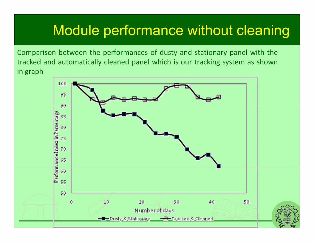
Module performance without cleaningComparison between the performances of dusty and stationary panel with thetracked and automatically cleaned panel which is our tracking system as shownin graph
Module Cleaning and Cost of Electricity
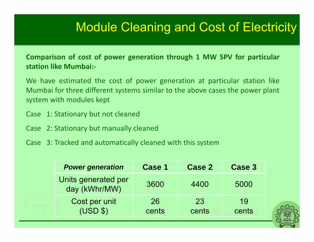
Comparison of cost of power generation through 1 MW SPV for particularstation like Mumbai:‐
We have estimated the cost of power generation at particular station likeMumbai for three different systems similar to the above cases the power plantsystem with modules kept
Case 1: Stationary but not cleaned
Case 2: Stationary but manually cleaned
Case 3: Tracked and automatically cleaned with this system
Power generation Case 1 Case 2 Case 3Power generation Case 1 Case 2 Case 3Units generated per
day (kWhr/MW) 3600 4400 5000
Cost per unit (USD $)
26cents
23cents
19cents
Thank you for your
Chetan S Solanki, IIT Bombay 65
attention