INDEX Code Exp Name of Experiment Date of Allotment … · · 2016-11-13Name of Experiment Date...
20
INDEX S.No Category of Assignme nt Code Exp eri men t No. Name of Experiment Date of Allotment of experiment Date of Evaluation Max. Marks Marks obtaine d Signature of Faculty 1. 1 Simulation using ORCAD 2. MANDATOR Y EXPERIMENT LR (10) 2 To simulate half adder circuit 3. 3 To simulate full adder circuit 4. 4 To simulate logical part of ALU 5. 5 To simulate four bit binary adder subtractor 6. 6 To simulate and study the tri-state buffer 7. 7 To simulate the common bus using tri-state buffers and decoder. 8. 8 To simulate the common bus using multiplexers.
Transcript of INDEX Code Exp Name of Experiment Date of Allotment … · · 2016-11-13Name of Experiment Date...

INDEX
S.No Category
of
Assignme
nt
Code Exp
eri
men
t
No.
Name of Experiment Date of
Allotment
of
experiment
Date of
Evaluation
Max.
Marks
Marks
obtaine
d
Signature
of Faculty
1.
1 Simulation
using ORCAD
2.
MANDATOR
Y
EXPERIMENT
LR
(10)
2 To simulate
half adder
circuit
3. 3 To simulate full
adder circuit
4. 4 To simulate
logical part of
ALU
5. 5 To simulate
four bit binary
adder subtractor
6. 6 To simulate and
study the tri-state
buffer
7. 7 To simulate the
common bus
using tri-state
buffers and
decoder.
8. 8 To simulate the
common bus
using
multiplexers.

9. 9 Study of 8085
Microprocessor
10. 10 Study of instruction
set of 8085
microprocessor.
11. 11. To simulate and
study 2:4 and 3:8
decoder.
12. Design
Based
Open
Ended
experimen
t**
PR
(10)
10
13. Viva Viva
(5)
5

EXPERIMENT NO.1
AIM: Simulation using ORCAD.
Digital Circuits
Procedure for simulation of circuits on ORCAD capture tool:
1) Click the capture lite icon from desktop or from the start menu.
2) Click on file, then on new, and then click on project.
3) Write the name of the project and choose the location to store it, then click “OK” and
make sure to choose analog or mixed A/D option and then again click “OK”.
4) Next pop-up window opens Pspice project on this choose a blank project option, then
click “OK”.
5) Now realize the circuits using proper components.
6) Now choose Pspice option on top toolbar and click on new simulation profile.
7) Enter the name of the profile and then click on “OK”.
8) In the next window choose options and then choose gate level simulation. Choose the
option and initialize all flip-flops to zero, then click on “OK”.
V place voltage where we need to see the outputs.
9) Lastly click the “Run” button in Pspice or Run option to see the resulting output.
Analog Circuits
Procedure for simulation of circuits on ORCAD capture tool:
The use of resistors and capacitors:-
1) Click on “place part” on the right hand side of the window. 2) Then click on analog library and select the required resistor and capacitor.
The use of Transistor:-
1) Click on “place part” on the right hand side of the window. 2) Click on the EVAL library and select the required transistor (E.G. Q2N2222).
The use of source:-
1) Click on “place part” on the right hand side of the window. 2) Then click on source library.

The use of ground:-
10) Click on ‘GND’ on the right hand side of the window. 11) Select CAPSYM library. 12) Select GND. 13) Click OK. 14) Edit properties to set “Name=0”.
To select the arrow in op-amp as a filter:-
1) Select the ‘(PWR/Q)’ from the right hand side of the window. 2) Select ‘Vcc_arrow’. 3) Name = V+ or V- 4) While using a dc source always use a DC source.
To change the value of any component:-
1) Select the component. 2) Right click on it. 3) Click “edit properties “. 4) Change the values of desired components.
To change the name of any component:-
1) Select NI on the right hand side of the window (not alias). 2) Change name. 3) Right click on it 4) Edit properties and click “OK”. 5) Box with the required name will be placed.
To change the direction of any of selected component:-
1) Place it on the required place and right click on it. 2) Select rotate and it will rotate by 90 degrees. 3) Select it as many times as rotation is required. 4) After placing all the components join them through the wire and you will obtain the
required circuit.
For Output:-
1) Click Pspice simulation. 2) Select new simulation. 3) Select analysis type which can be different for different experiments.

EXPERIMENT NO.2
AIM: To design the circuit of half adder.
IC USED: 7486(X-OR), 7408(AND).
THEORY: A half adder is a logical circuit that performs an additional operation on two binary
digits. The half adder produces a sum and a carry value which are both binary digits.
A half adder circuit has two inputs A and B and two outputs – S representing sum and C
representing carry.
S = A xor B i.e. (A’B + AB’)
C = A and B i.e. (A.B)
TRUTH TABLE:
A B S C
0 0 0 0
0 1 1 0
1 0 1 0
1 1 0 1

SCHEMATIC DIAGRAM:
WAVEFORM:
RESULT: The output waveform of half adder is verified.

EXPERIMENT NO.3
AIM: To design the circuit of full adder.
IC USED: 7486(X-OR), 7408(AND), 7432(OR).
THEORY: A full adder is a logical circuit that performs an additional operation on three binary
digits. The half adder produces a sum and a carry value which are both binary digits.
A full adder circuit has three inputs A,B and Cin and two outputs – S representing sum and Cout
representing carry.
S = A xor B xor C
C = A.B +C(A xor B)
TRUTH TABLE:
A B Cin S Cout
0 0 0 0 0
0 0 1 1 0
0 1 0 1 0
0 1 1 0 1
1 0 0 1 0
1 0 1 0 1

1 1 0 0 1
1 1 1 1 1
SCHEMATIC DIAGRAM:
WAVEFORM:
RESULT: The output waveform of Full Adder is verified.

EXPERIMENT NO.4
AIM: To design logical part of ALU.
IC USED: 74153(4×1 MUX), 7432(OR), 7404(NOT), 7408(AND), 7486(XOR).
THEORY: In computing, an arithmetic logic unit (ALU) is a digital circuit that performs
arithmetic and logical operations. The ALU is a fundamental building block of the central
processing unit (CPU) of a computer, and even the simplest microprocessors contain one for
purposes such as maintaining timers. The processors found inside modern CPUs and graphics
processing units (GPUs) accommodate very powerful and very complex ALUs; a single
component may contain a number of ALUs.
Mathematician John von Neumann proposed the ALU concept in 1945.
Below is a block diagram for an ALU:
Truth table of the ALU
S1 S0 OUTPUT
0 0 A and B
0 1 A or B
1 0 A xor B
1 1 Not A

SCHEMATIC:
WAVEFORM:
RESULT: The ALU is designed and its output is verified.

EXPERIMENT NO.5
AIM: To design a 4-bit adder subtractor.
IC USED: 7483A (4-bit adder), 7486(X-OR).
THEORY: It is a combinational circuit which can act as both a binary adder and a binary
subtractor. It is constructed using 4 full adders. Block diagram of the circuit is shown below:
In this case if sub is 0, then the circuit acts as an adder,else subtractor. Subtraction is done by
adding two’s compliment of B to A, which effectively results in A - B.
SCHEMATIC DIAGRAM:

WAVEFORM:
RESULT: The circuit of a 4-Bit adder subtractor is designed and verified.

EXPERIMENT NO.6
Aim: To simulate and study the tristate buffer.
ICs used: Tri state buffer 74125 Theory: In digital electronics three-state, tri-state, or 3-state logic allows an output port to assume a high
impedance state in addition to the 0 and 1 logic levels, effectively removing the output from the circuit.
This allows multiple circuits to share the same output line or lines (such as a bus).
Truth Table
A Tri-state Buffer
A Q
0 0
1 1
Boolean Expression Q = A Read as A gives Q
The "Tri-state Buffer"As well as the standard Digital Buffer seen above, there is another type of digital
Buffer circuit whose output can be "electronically" disconnected from its output circuitry when required.
This type of Buffer is known as a 3-State Buffer or commonly Tri-state Buffer.
A Tri-state Buffer can be thought of as an input controlled switch which has an output that can be
electronically turned "ON" or "OFF" by means of an external "Control" or "Enable" signal input. This
control signal can be either a logic "0" or a logic "1" type signal resulting in the Tri-state Buffer being in
one state allowing its output to operate normally giving either a logic "0" or logic "1" output. But when
activated in the other state it disables or turns "OFF" its output producing an open circuit condition that is
neither "High" or "low", but instead gives an output state of very high impedance, high-Z, or more
commonly Hi-Z. Then this type of device has two logic state inputs, "0" or a "1" but can produce three
different output states, "0", "1" or "Hi-Z" which is why it is called a "3-state" device.
There are two different types of Tri-state Buffer, one whose output is controlled by an "Active-HIGH"
control signal and the other which is controlled by an "Active-LOW" control signal, as shown below.
Active "HIGH" Tri-state Buffer
Symbol Truth Table
Enable A Q
1 0 0

Tri-state Buffer 1 1 1
0 0 Hi-Z
0 1 Hi-Z
Read as Output = Input if Enable is equal to "1"
An Active-high Tri-state Buffer is activated when a logic level "1" is applied to its "enable" control line
and the data passes through from its input to its output. When the enable control line is at logic level "0",
the buffer output is disabled and a high impedance condition, Hi-Z is present on the output.
Active "LOW" Tri-state Buffer
Symbol Truth Table
Tri-state Buffer
Enable A Q
0 0 0
0 1 1
1 0 Hi-Z
1 1 Hi-Z
Read as Output = Input if Enable is NOT equal to "1"
An Active-low Tri-state Buffer is the opposite to the above, and is activated when a logic level "0" is
applied to its "enable" control line. The data passes through from its input to its output. When the enable
control line is at logic level "1", the buffer output is disabled and a high impedance condition, Hi-Z is
present on the output.
SCHEMATIC DIAGRAM:

WAVEFORM:
RESULT: The truth table of the tri-state buffer should match with the simulation graph of the tri-state
buffer .

EXPERIMENT NO. 7
Aim: To simulate the common bus using tri-state buffers and decoder.
Software Used: ORCAD Capture
Theory: A bus system can be constructed with three-state gates instead of multiplexers. A three-state gate
is a digital circuit that exhibits three states. Two of these states are signals equivalent to logic 1 and 0 as in
conventional gate. The third state is a high-impedance state. The high-impedance state behaves like an
open circuit, which means that the output is disconnected and does not have a logic significance. Three-
state gates may perform any conventional logic, such as AND or NAND. However, the one most
commonly used in the design of a bus system is the buffer gate.
The construction of a bus system with three-state buffers is demonstrated below. The outputs of four
buffers are connected together to form a single bus line. The control inputs to the buffers determine which
of the four normal inputs will communicate with the bus line. No more than one buffer may be in the
active state at any given time. The connected buffers must be controlled so that only one three-state buffer
has access to the bus line while all other buffers are maintained in a high-impedance state.
One way to ensure that no more than one control input is active at any given time is to use a decoder, as
shown in the diagram. When the enable input of the decoder is 0, all of its four outputs are 0, and the bus
line is in a high-impedance state because all four buffers are disabled. When the enable input is active,
one of the three-state buffers will be active, depending on the binary value in the select inputs of the
decoder. Careful investigation will reveal that the figure below is another way of constructing a 4x1
multiplexer since the circuit can be replaced as one would make a bus system with a multiplexer.

SCHEMATIC DIAGRAM:
WAVEFORM:
RESULT: The circuit of common bus using tri-state buffers and decoder is designed and
verified.

EXPERIMENT NO. 11
AIM: To simulate and design a 2:4 and 3:8 decoders.
IC USED: 7404(NOT), 7408(AND).
THEORY: A decoder is a device which does the reverse of an encoder, undoing the encoding so
that the original information can be retrieved. The same method used to encode is usually just
reversed in order to decode.
In digital electronics, a decoder can take the form of a multiple-input, multiple-output logic
circuit that converts coded inputs into coded outputs, where the input and output codes are
different.
Decoders have 3 inputs and 8 outputs. The binary input fed at input will be decoded to provide
either logical high or low on one of the 8 outputs, which is termed as octal equivalent for that
binary input. For a binary input 100, which is 4 in octal number system, the output pin called
O4 will go either high or low.
Truth table for 2:4 Decoder:
.
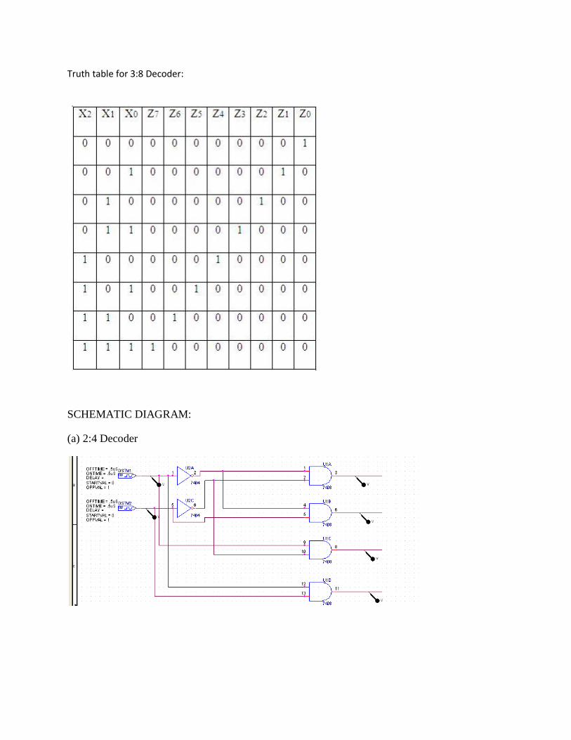
Truth table for 3:8 Decoder:
SCHEMATIC DIAGRAM:
(a) 2:4 Decoder

(b) 3:8 Decoder
WAVEFORM:
(a) 2:4 Decoder:
(b) 3:8 Decoder
RESULT: 2:4 and 3:8 decoder are designed and outputs are verified.