Incorporating DFT into your 3D Chip Stack Design Flo/media... · Incorporating DFT into your 3D...
35
Incorporating DFT into your 3D Chip Stack Design Flow Instructions: Audio on 1-877-669-3239 Password 3DIC Upon joining, please mute your phone Please feel free to direct comments or questions to the meeting host or attendees, using the chat window in the right hand pane of the Webex meeting tool July 11, 2011 1 Incorporating DFT into your 3D Chip Stack Design Flow
Transcript of Incorporating DFT into your 3D Chip Stack Design Flo/media... · Incorporating DFT into your 3D...

Incorporating DFT into your 3D
Chip Stack Design Flow
Instructions:Audio on 1-877-669-3239
Password 3DIC
Upon joining, please mute your phone
Please feel free to direct comments or questions to the
meeting host or attendees, using the chat window in the right
hand pane of the Webex meeting tool
July 11, 2011 1Incorporating DFT into your 3D Chip Stack Design Flow
Incorporating DFT into your 3D
Chip Stack Design Flow
Hsu Ho, Jeetendar Narsinghani, Hudson An,
Robert Mallard
CMC Microsystems
July 11, 2011
July 11, 2011 2Incorporating DFT into your 3D Chip Stack Design Flow
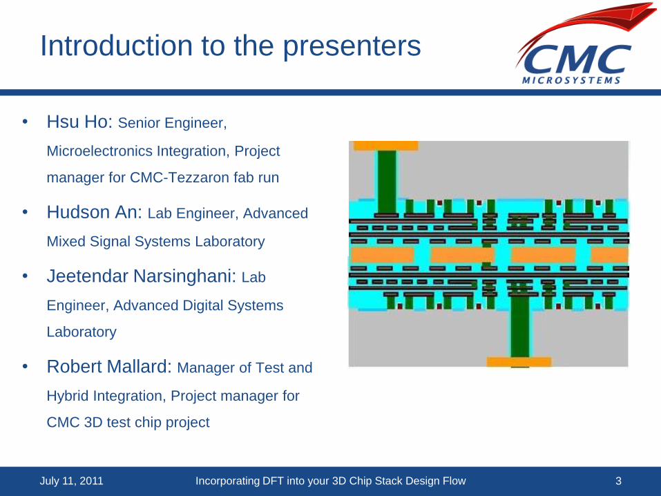
Introduction to the presenters
• Hsu Ho: Senior Engineer,
Microelectronics Integration, Project
manager for CMC-Tezzaron fab run
• Hudson An: Lab Engineer, Advanced
Mixed Signal Systems Laboratory
• Jeetendar Narsinghani: Lab
Engineer, Advanced Digital Systems
Laboratory
• Robert Mallard: Manager of Test and
Hybrid Integration, Project manager for
CMC 3D test chip project
July 11, 2011 3Incorporating DFT into your 3D Chip Stack Design Flow
3D IC stacking
Pilot fab run through CMC
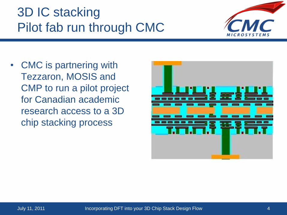
• CMC is partnering with
Tezzaron, MOSIS and
CMP to run a pilot project
for Canadian academic
research access to a 3D
chip stacking process
July 11, 2011 4Incorporating DFT into your 3D Chip Stack Design Flow

Scope of CMC 3D Test Chip Project
• Develop a “reference design” mixed signal
microelectronic test chip based on a 3D
chip stacking architecture / process:
– exploring application of DFT in a 3D IC design
flow
• Process test structures for gaining a better
understanding of the technology
– Structures include TSV chain, TSV
characterization structures, bond metal chain,
ring oscillator, amplifier, individual MOS devices
on top & bottom tiers, photo diode for backside
illumination, etc.
• The chips will be made available to the
community; we welcome your input on
what additional test structures to include
July 11, 2011 5Incorporating DFT into your 3D Chip Stack Design Flow

CMC 3D Test Chip Project Outputs
• Fabricated chips (packaged parts and loose die)
• Mixed signal design files (schematic, RTL, layout, script file)
• Application notes
– describing the design flow used for the reference design and step-
by-step design execution instructions
– describing the test plan and its implementation
• Series of webinars linking project outputs and related
technologies
– Emphasis on design flow to address testability in a 3D IC stack
• JTAG, CAD environment, insertion of 1149.1 in an ASIC design, next generation
DFT approaches, industry perspectives on importance of DFT
July 11, 2011 6Incorporating DFT into your 3D Chip Stack Design Flow

Objectives of today‟s webinar
• What is the design flow?
• How does DFT enter into the
flow?
• What tools are required to
implement the design?
• What issues have arisen to date
during the CMC 3D IC test chip
project?
July 11, 2011 7Incorporating DFT into your 3D Chip Stack Design Flow
Objectives of today‟s webinar
• The presentation may raise as
many questions as it answers
• We‟re interested in your
feedback:
– How well does the flow work for
academic users of the
technology?
– What is missing?
– Alternate approaches available?
– How can the flow be improved?
July 11, 2011 8Incorporating DFT into your 3D Chip Stack Design Flow
Overview
• Description of Tezzaron chip
stacking technology available
through CMC
• 3D IC test challenges
• High level test strategy
• Overview of CMC 3D IC test chip
• Overview of design flow
• Incorporation of DFT in design
flow
July 11, 2011 9Incorporating DFT into your 3D Chip Stack Design Flow

Tezzaron 3D-IC Technology with
Fine-Pitch TSV
• MOSIS/CMP/CMC in partnership for the offering of
MPW service based on Tezzaron‟s SuperContact
technology and GlobalFoundries‟ 0.13um CMOS LP
process
• Technology specifics:
• Middle-of-line TSV process
• 2-tier face-to-face wafer bond
• 0.13um CMOS for both top and bottom tier: 6 metal
layers, 1.5V/3.3V MOS devices
• Only top tier thinned to expose TSV
• Backside metal on top tier allowing flip-chip
attachment of user device or wire bond
Inter-tier connection by top
metal bond (not TSV)
IO through backside metal
July 11, 2011 10Incorporating DFT into your 3D Chip Stack Design Flow

Tezzaron 3D-IC Technology with
Fine-Pitch TSV
• Physical design kit (PDK) supporting 3D-IC design
with ARM cell libraries is available. PDK is primarily
based on the following CAD products:
• Cadence‟s Spectre, Virtuoso, Encounter, Assura for
design capture, circuit simulation, manual layout,
automatic place & route and layer fill
• Mentor Graphics„ Calibre for DRC and 3D LVS
• Synopsys‟ Design Vision for digital synthesis
Inter-tier connection by top
metal bond (not TSV)
IO through backside metal
July 11, 2011 11Incorporating DFT into your 3D Chip Stack Design Flow

Tezzaron 3D-IC Technology with
Fine-Pitch TSV
• Thinning of bottom-tier die to connect to the
TSV may be done outside of the MPW
services by third-party sources (e.g. Ziptronix)
July 11, 2011 12Incorporating DFT into your 3D Chip Stack Design Flow
3D Chip Stacks: Test challenges
• Test, de-bug and isolate faults
• Top die is the only with I/O access,
delivering test patterns to the bottom
die in a packaged stack
• Ability to isolate each tier to run
scan based tests
• Is the interconnect reliable?
• Test the interconnect!
• Known good die (KGD) requirements
to be met
• Wafer level probing
• Cost !!!!
July 11, 2011 13Incorporating DFT into your 3D Chip Stack Design Flow

• Wafer level pre-screen of individual die
• System functional tests through primary I/O
• System power/ground/shorts test via primary I/O
• JTAG 1149.1 tests for tier to tier (and general) interconnect
• Inaccessible test points are to be bi-directional, allowing 1149.1
testing for connectivity
• 1149.1 for low speed functional testing
• “At speed” testing using BIST (memory, analog, logic where
needed)
• Implementation of function-specific embedded instrumentation,
compliance with p1687
• Digital (1149.1) access to all embedded instruments (including
BIST)
3D IC stack testing
Generalized high level test strategy
July 11, 2011 14Incorporating DFT into your 3D Chip Stack Design Flow
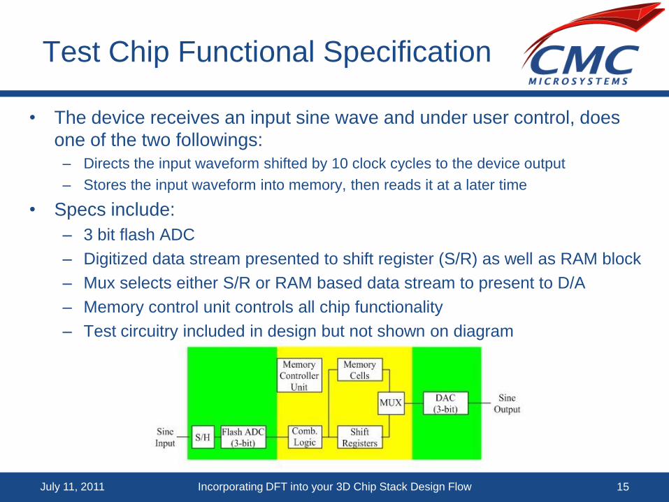
Test Chip Functional Specification
• The device receives an input sine wave and under user control, does
one of the two followings:
– Directs the input waveform shifted by 10 clock cycles to the device output
– Stores the input waveform into memory, then reads it at a later time
• Specs include:
– 3 bit flash ADC
– Digitized data stream presented to shift register (S/R) as well as RAM block
– Mux selects either S/R or RAM based data stream to present to D/A
– Memory control unit controls all chip functionality
– Test circuitry included in design but not shown on diagram
July 11, 2011 15Incorporating DFT into your 3D Chip Stack Design Flow
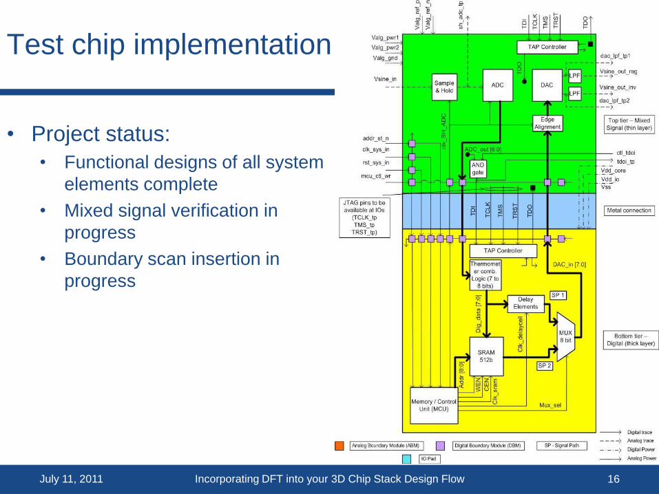
Test chip implementation
• Project status:
• Functional designs of all system
elements complete
• Mixed signal verification in
progress
• Boundary scan insertion in
progress
July 11, 2011 16Incorporating DFT into your 3D Chip Stack Design Flow

Design Flow and CAD Toolset for
3D IC stack (excluding DFT)
•The following slides schematically describe the
flow for a general 3D IC stack design
•general design flow
•further details on
•single-tier block assembly
•3D LVS
•The flow is similar to 2D flow except for steps in
filled boxes
July 11, 2011 17Incorporating DFT into your 3D Chip Stack Design Flow
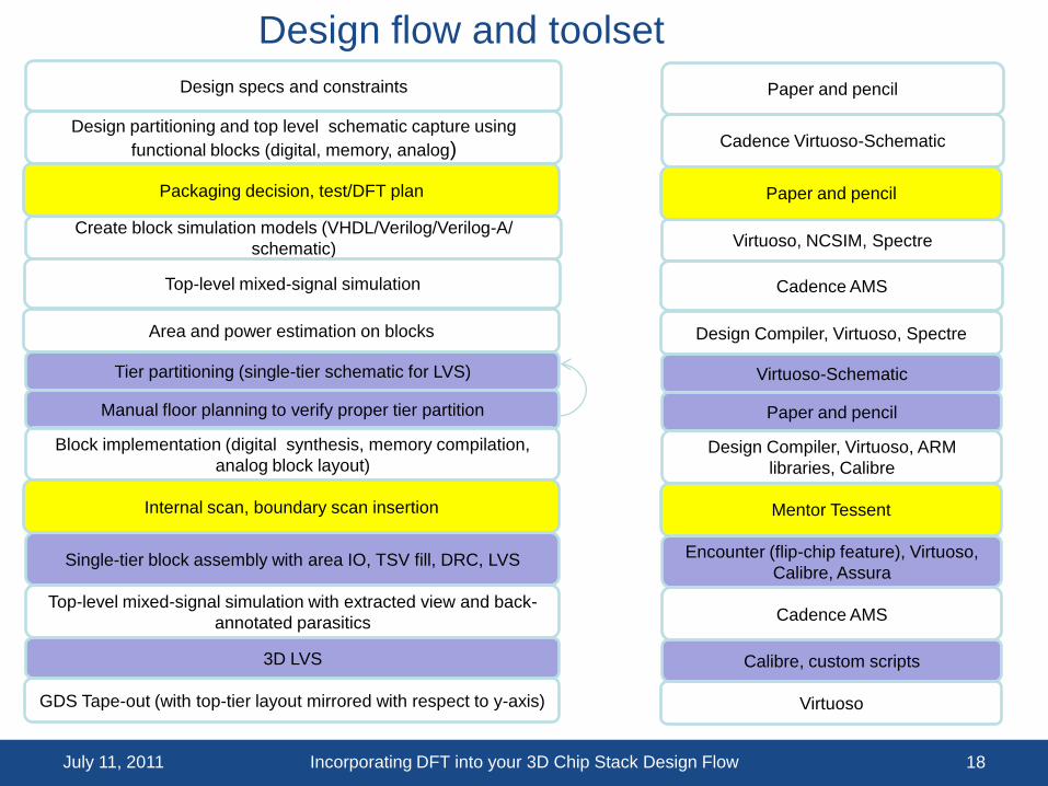
Design flow and toolset
July 11, 2011 18Incorporating DFT into your 3D Chip Stack Design Flow
Paper & pencil
Cadence Virtuoso-Schematic
Cadence Virtuoso-Schematic,
NCSIM, Spectre
Cadence AMS
Design Vision, Virtuoso-Layout
Virtuoso-Schematic
Paper & pencil
Design Vision, Virtuoso, ARM
librariesEncounter, Virtuoso, Calibre,
Assura
Cadence AMS
Calibre
Virtuoso
Design specs and constraints
Design partitioning and top level schematic capture using
functional blocks (digital, memory, analog)
Create block simulation models (VHDL/Verilog/Verilog-A/
schematic)
Top-level mixed-signal simulation
Area and power estimation on blocks
Tier partitioning (single-tier schematic for LVS)
Manual floor planning to verify proper tier partition
Block implementation (digital synthesis, memory compilation,
analog block layout)
Single-tier block assembly with area IO, TSV fill, DRC, LVS
Top-level mixed-signal simulation with extracted view and back-
annotated parasitics
3D LVS
GDS Tape-out (with top-tier layout mirrored with respect to y-axis)
Internal scan, boundary scan insertion
Packaging decision, test/DFT plan
Design specs, performance metrics, design
constraints, packaging requirements
Top-level schematic with functional blocks
(digital, memory, analog)
Block simulation model (VHDL/Verilog/Verilog-A/
schematic)
Top-level mixed-signal simulation
Digital synthesis and preliminary analog layout
for block area estimation
Tier partitioning (single-tier schematic for LVS)
Manual floor planning to verify proper tier
partition
Digital block synthesis, memory compilation,
analog block layout implementation
Single-tier block assembly, DRC, LVS, extraction
Top-level mixed-signal simulation with extracted
view and back-annotated parasitics
3D LVS
GDS Tape-out (with top-tier layout mirrored with
respect to y-axis)
Paper and pencil
Cadence Virtuoso-Schematic
Virtuoso, NCSIM, Spectre
Cadence AMS
Design Compiler, Virtuoso, Spectre
Virtuoso-Schematic
Paper and pencil
Design Compiler, Virtuoso, ARM
libraries, Calibre
Encounter (flip-chip feature), Virtuoso,
Calibre, Assura
Cadence AMS
Calibre, custom scripts
Virtuoso
Mentor Tessent
Paper and pencil
DFT Agenda
• Why DFT?
• 3D IC Testing – Approach
• DFT Insertion
• Interconnect Tests
• Testing Analog Circuits & Memory using 1149.1
• DFT flow – Boundary & Internal Scan
• Test Equipment
July 11, 2011 Incorporating DFT into your 3D Chip Stack Design Flow 19
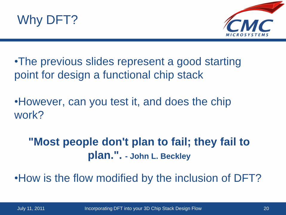
Why DFT?
July 11, 2011 Incorporating DFT into your 3D Chip Stack Design Flow 20
•The previous slides represent a good starting
point for design a functional chip stack
•However, can you test it, and does the chip
work?
"Most people don't plan to fail; they fail to
plan.". - John L. Beckley
•How is the flow modified by the inclusion of DFT?

3D IC Test Approach
• Functional Tests– Open and shorts tests: Primary I/O
– Power Bus Shorts Test
– System functional tests through primary I/O
• Debug Mode– JTAG 1149.1 tests for tier to tier interconnect
– Monitor inaccessible nets (test points)
– Individual Block level tests using internal scan (Digital)
– Analog circuit tests using JTAG 1149.1
• Other tests (optional)– Power measurements
– Shmoo tests (Freq vs. Vdd)
July 11, 2011 Incorporating DFT into your 3D Chip Stack Design Flow 21

DFT Insertion
• Boundary Scan on MS and Digital Tier– TAP ports accessible from top
MS tier
– TAP Controller
– Instruction and data registers
– Boundary scan cells
• Internal scan on Digital Tier– Functional testing
– Fault detection and diagnosis (S-A-X)
• MS and Digital Tier connected at metal layer
• Option to control each tier individually
July 11, 2011 Incorporating DFT into your 3D Chip Stack Design Flow 22

Interconnect Tests
• Chain Integrity Test
– Dead chain
– Broken connection
• Testing shorts and
opens (metal
bonding)
• Interaction tests
– Ports not connected to
BSC
• Bi-directional IOs
July 11, 2011 Incorporating DFT into your 3D Chip Stack Design Flow 23
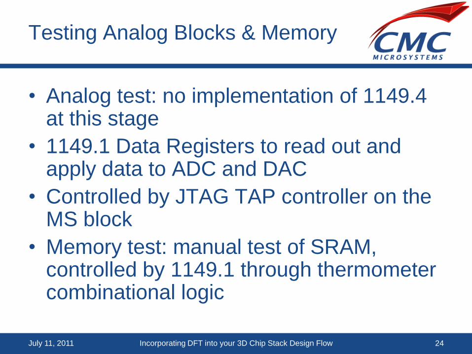
Testing Analog Blocks & Memory
• Analog test: no implementation of 1149.4 at this stage
• 1149.1 Data Registers to read out and apply data to ADC and DAC
• Controlled by JTAG TAP controller on the MS block
• Memory test: manual test of SRAM, controlled by 1149.1 through thermometer combinational logic
July 11, 2011 24Incorporating DFT into your 3D Chip Stack Design Flow
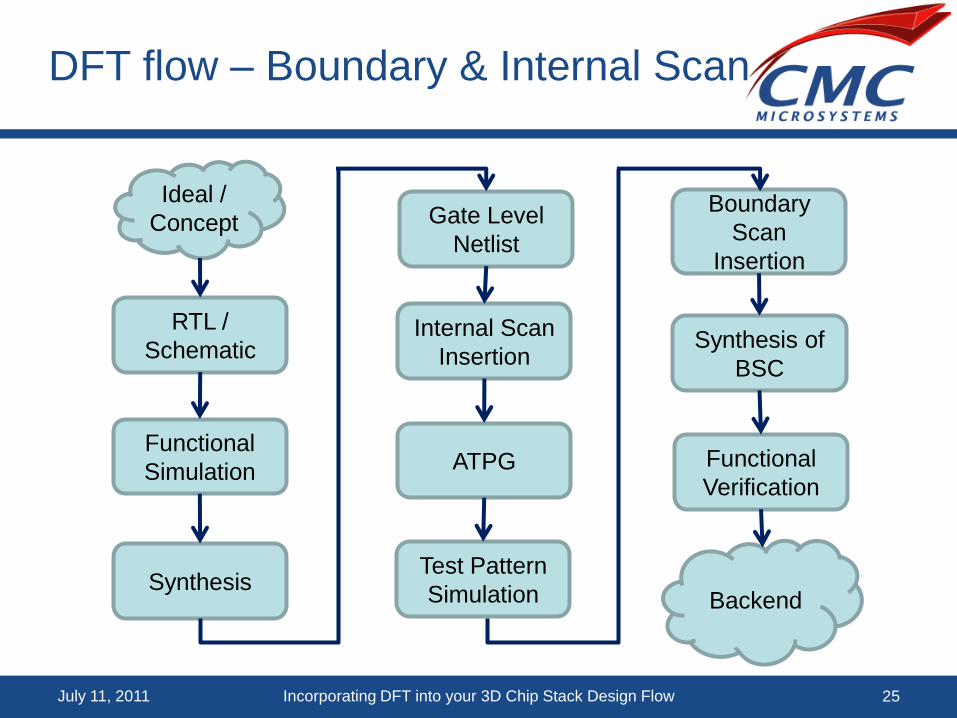
DFT flow – Boundary & Internal Scan
July 11, 2011 Incorporating DFT into your 3D Chip Stack Design Flow 25
RTL /
Schematic
Synthesis
Internal Scan
Insertion
Boundary
Scan
Insertion
ATPG
Test Pattern
Simulation
Functional
Simulation
Gate Level
Netlist
Synthesis of
BSC
Functional
Verification
Ideal /
Concept
Backend
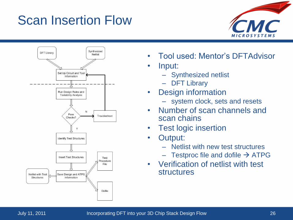
Scan Insertion Flow
• Tool used: Mentor‟s DFTAdvisor
• Input: – Synthesized netlist
– DFT Library
• Design information– system clock, sets and resets
• Number of scan channels and scan chains
• Test logic insertion
• Output:– Netlist with new test structures
– Testproc file and dofile ATPG
• Verification of netlist with test structures
July 11, 2011 Incorporating DFT into your 3D Chip Stack Design Flow 26

Boundary Scan Flow
• Tool used: Mentor‟s BSDArchitect
• Input: HDL Entity of top-level
• Run BSDArchitect
• Outputs:– HDL with BS inserted
(_bscan)
– IO description of top-level BS entity (_top)
– HDL test bench (_tb)
– BSDL description of BS (_bscan.bsd)
– Testproc and dofile ATPG
– WGL format test vectors
• Synthesize BS Logic
• Boundary Scan Verification
July 11, 2011 Incorporating DFT into your 3D Chip Stack Design Flow 27

Design flow and toolset
July 11, 2011 28Incorporating DFT into your 3D Chip Stack Design Flow
Paper & pencil
Cadence Virtuoso-Schematic
Cadence Virtuoso-Schematic,
NCSIM, Spectre
Cadence AMS
Design Vision, Virtuoso-Layout
Virtuoso-Schematic
Paper & pencil
Design Vision, Virtuoso, ARM
librariesEncounter, Virtuoso, Calibre,
Assura
Cadence AMS
Calibre
Virtuoso
Design specs and constraints
Design partitioning and top level schematic capture using
functional blocks (digital, memory, analog)
Create block simulation models (VHDL/Verilog/Verilog-A/
schematic)
Top-level mixed-signal simulation
Area and power estimation on blocks
Tier partitioning (single-tier schematic for LVS)
Manual floor planning to verify proper tier partition
Block implementation (digital synthesis, memory compilation,
analog block layout)
Single-tier block assembly with area IO, TSV fill, DRC, LVS
Top-level mixed-signal simulation with extracted view and back-
annotated parasitics
3D LVS
GDS Tape-out (with top-tier layout mirrored with respect to y-axis)
Internal scan, boundary scan insertion
Packaging decision, test/DFT plan
Design specs, performance metrics, design
constraints, packaging requirements
Top-level schematic with functional blocks
(digital, memory, analog)
Block simulation model (VHDL/Verilog/Verilog-A/
schematic)
Top-level mixed-signal simulation
Digital synthesis and preliminary analog layout
for block area estimation
Tier partitioning (single-tier schematic for LVS)
Manual floor planning to verify proper tier
partition
Digital block synthesis, memory compilation,
analog block layout implementation
Single-tier block assembly, DRC, LVS, extraction
Top-level mixed-signal simulation with extracted
view and back-annotated parasitics
3D LVS
GDS Tape-out (with top-tier layout mirrored with
respect to y-axis)
Paper and pencil
Cadence Virtuoso-Schematic
Virtuoso, NCSIM, Spectre
Cadence AMS
Design Compiler, Virtuoso, Spectre
Virtuoso-Schematic
Paper and pencil
Design Compiler, Virtuoso, ARM
libraries, Calibre
Encounter (flip-chip feature), Virtuoso,
Calibre, Assura
Cadence AMS
Calibre, custom scripts
Virtuoso
Mentor Tessent
Paper and pencil

Test equipment
• Bench top
• ATE
• Vectors
• Requires BSDL file
– Test equipment
July 11, 2011 Incorporating DFT into your 3D Chip Stack Design Flow 29

• TSV integrity
• As TSV process maturity (yield) is imperfect, inclusion
of redundant tier to tier interconnect is an advisable
strategy
• In the CMC 3D test chip:
• Primary I/O is TSV
• Inclusion of redundant interconnect is viable as the TSV is
significantly smaller than the bond metal pattern; The IO
cells in the kit already have a TSV wrapper with a lot of
TSVs for each pad.
• Tier to tier interconnect is face to face
• 2x2 bond pad redundancy will be employed
• Will they all be tested using 1149.1?
Further design considerations
July 11, 2011 30Incorporating DFT into your 3D Chip Stack Design Flow
Possible gotchas
• Limitations of 1149.4 when large numbers of pins needed:
• Area intensive due to interconnect length/logic, DC leakage issues
• Some innovative solutions discussed in Steve Sunter‟s
presentation of June 20 (e.g. on-chip ADC, comparators, special
case of SerDes)
• Similar area cost issues for TSV test using 1149.1 if tier to
tier interconnect density becomes too high?
• What implications for chip/system design if TSV integrity never
manages to reach the quality levels of in-plane interconnect?
• Fault tolerance, redundancy
• KGD
• Supply chain issues: availability of die, accessibility of BSDL files
July 11, 2011 31Incorporating DFT into your 3D Chip Stack Design Flow

July 11, 2011 32Incorporating DFT into your 3D Chip Stack Design Flow
Summary
• 3D IC stacks pose some inherent
testability challenges
• Many of these challenges can be
addressed using existing test
standards and methods
• The CAD environment supporting
3D design is rapidly evolving; the
inclusion of DFT requires some
relatively straightforward additions
to the basic flow
• A proper test approach involves
requires rigorous planning at the
design inception stage

Stay in touch with the project
Questions and comments? Contact Rob Mallard at [email protected]
For regular updates on upcoming webinars in this series:
http://www.cmc.ca/en/NewsAndEvents/Events/3DIC_WebinarSeries.aspx
July 11, 2011 33Incorporating DFT into your 3D Chip Stack Design Flow
For more information
•First fab run has a Sept 19 design submission deadline
July 11, 2011 34Incorporating DFT into your 3D Chip Stack Design Flow
CMC 3D IC Test
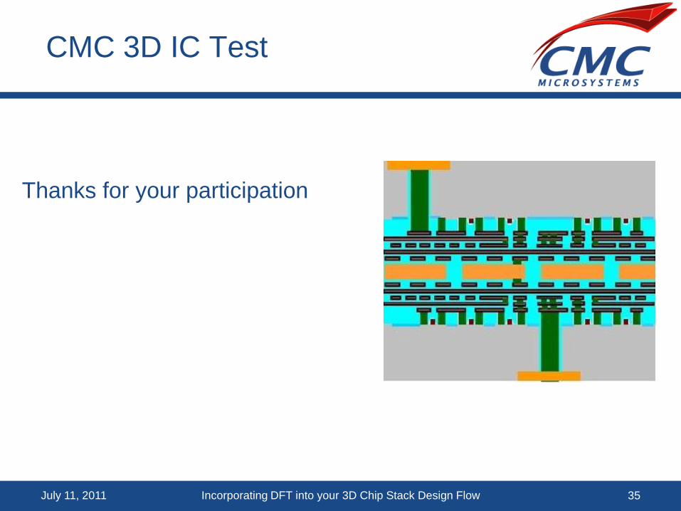
Thanks for your participation
July 11, 2011 35Incorporating DFT into your 3D Chip Stack Design Flow