Inclusion Voiding in Gull Wing Solder Joints · Inclusion Voiding in Gull Wing Solder Joints T.L....
27
Inclusion Voiding in Gull Wing Solder Joints T.L. Lewis 1 , C.O. Ndiaye 2 and J.R. Wilcox 3 IBM Corporation 1 Rochester, MN, 2 Poughkeepsie, NY, 3 Endicott, NY Abstract Solder voiding in ball grid array (BGA) solder joints has been well characterized and documented in IPC-A-610 and IPC- 7095 which define industry recommended BGA solder workmanship criteria and methods of inspection. Solder voiding limits associated with other, non-BGA, Surface Mount Technology (SMT) solder joint types however are neither well defined nor well understood in the industry. According to IPC guidelines, the amount and size of solder voids are simply to be specified by customer/vendor agreement. In the absence of well defined voiding criteria though, the morphology of solder joint fillets seen in final visual inspection often becomes the sole arbiter of solder workmanship and quality. Among the various SMT solder interconnect designs used in IBM applications, one of the more common SMT leaded structures is the Gull Wing design found on SMT connectors. Three distinct types of solder voiding have been observed in these Gull Wing solder joints: solder inclusion voids, solder exclusion voids, and solidification hot tears. The most prevalent of the three has been inclusion voids, also known as solder process voids. Such solder inclusion voids in SMT leaded solder joints have been observed using either IR/convection or vapor phase reflow processes. This paper provides definitions of the different voiding types encountered in Gull Wing solder joint geometries. It further provides corresponding reliability data that support some level of inclusion voiding in these solder joints and identifies the final criteria being applied for certain IBM Server applications. Such acceptance criteria can be applied using various available x-ray inspection techniques on a production or sample basis. The bulk of supporting data to date has been gathered through RoHS server exempt SnPb eutectic soldering operations but it is expected to provide a reasonable baseline for pending Pb-free solder applications. Background Solder voiding has been a common phenomenon in mass reflow soldering processes used in the server/telecomm industries, being variously characterized as process anomalies, process indicators and/or solder defects. As surface mount technologies (SMT) have taken precedence over Pin through Hole (PTH) technologies, Ball Grid Array (BGA) components have been the main vehicle for industry classification of solder joint voiding. A solder void is defined here as a hole or enclosed volume of space within the solder joint that lacks solder material. This space may be comprised of a combination of gas, solid residues and liquid non-metallic materials or possibly vacuum. The main classifications of solder voiding within BGA and PTH soldering applications have been identified by Aspandiar [1] as the following: Inclusion / Macrovoids – Voids containing byproducts that result from fluxing reactions inherent to the solder reflow/melting process. Also known as process voids, these voids generally do not affect interconnect reliability unless they are present at interfacial regions of the solder joints where cracks can form or they accumulate at other regions of local stress concentration. Planar Microvoids – Small voids residing substantially in a common plane at the interface between the printed circuit board (PCB) lands and the solder. These voids are uncommon on PCBs using OSP finishes but can occasionally be found on PCBs with fusible metal surface finishes such as immersion silver [2]. Such metal surface finishes can entrap hollow caverns within the finish deposit as an artifact of the deposition process. These caverns would in turn locally outgas during soldering to produce fine arrays of interfacial voids. Planar microvoids are generally not detectable in time zero functionality test but can seriously degrade solder joint reliability. Shrinkage Voids – Voids caused by the volume shrinkage of the solder alloy on the phase change from liquid to solid. There is a low incidence of shrinkage voids in SnPb eutectic soldering. They are seen more frequently with SnAgCu solder alloys. These voids necessarily form in the regions of the joint that are last to solidify, most frequently in the middle regions of the solder joint furthest removed from the interfacial intermetallic regions formed between the solder and base metals of the components leads or PCB lands. There are no documented instances showing that shrinkage voids affect solder joint reliability. Micro-via Voids – Voids that are formed from the outgassing of micro-vias in a PCB land, either capped or open. Voids are usually a consequence of solder reflow and the characteristics of the micro-via. Large micro-via voids located in stress concentration points within solder joints and high stress areas of a package can possibly affect reliability of the interconnect [3]. Intermetallic Microvoids – Voids that form within the intermetallic compound (IMC) between the base metal of the component lead or PCB land and the solder. These voids do not form immediately during the soldering process, but grow after extended thermal aging. IMC microvoids can substantially degrade the interconnect reliability through embrittlement of the interfaces [4].
Transcript of Inclusion Voiding in Gull Wing Solder Joints · Inclusion Voiding in Gull Wing Solder Joints T.L....
Inclusion Voiding in Gull Wing Solder Joints
T.L. Lewis1, C.O. Ndiaye
2 and J.R. Wilcox
3
IBM Corporation 1Rochester, MN,
2Poughkeepsie, NY,
3Endicott, NY
Abstract
Solder voiding in ball grid array (BGA) solder joints has been well characterized and documented in IPC-A-610 and IPC-
7095 which define industry recommended BGA solder workmanship criteria and methods of inspection. Solder voiding
limits associated with other, non-BGA, Surface Mount Technology (SMT) solder joint types however are neither well
defined nor well understood in the industry. According to IPC guidelines, the amount and size of solder voids are simply to
be specified by customer/vendor agreement. In the absence of well defined voiding criteria though, the morphology of solder
joint fillets seen in final visual inspection often becomes the sole arbiter of solder workmanship and quality. Among the
various SMT solder interconnect designs used in IBM applications, one of the more common SMT leaded structures is the
Gull Wing design found on SMT connectors. Three distinct types of solder voiding have been observed in these Gull Wing
solder joints: solder inclusion voids, solder exclusion voids, and solidification hot tears. The most prevalent of the three has
been inclusion voids, also known as solder process voids. Such solder inclusion voids in SMT leaded solder joints have been
observed using either IR/convection or vapor phase reflow processes. This paper provides definitions of the different voiding
types encountered in Gull Wing solder joint geometries. It further provides corresponding reliability data that support some
level of inclusion voiding in these solder joints and identifies the final criteria being applied for certain IBM Server
applications. Such acceptance criteria can be applied using various available x-ray inspection techniques on a production or
sample basis. The bulk of supporting data to date has been gathered through RoHS server exempt SnPb eutectic soldering
operations but it is expected to provide a reasonable baseline for pending Pb-free solder applications.
Background
Solder voiding has been a common phenomenon in mass reflow soldering processes used in the server/telecomm industries,
being variously characterized as process anomalies, process indicators and/or solder defects. As surface mount technologies
(SMT) have taken precedence over Pin through Hole (PTH) technologies, Ball Grid Array (BGA) components have been the
main vehicle for industry classification of solder joint voiding. A solder void is defined here as a hole or enclosed volume of
space within the solder joint that lacks solder material. This space may be comprised of a combination of gas, solid residues
and liquid non-metallic materials or possibly vacuum. The main classifications of solder voiding within BGA and PTH
soldering applications have been identified by Aspandiar [1] as the following:
Inclusion / Macrovoids – Voids containing byproducts that result from fluxing reactions inherent to the solder
reflow/melting process. Also known as process voids, these voids generally do not affect interconnect reliability
unless they are present at interfacial regions of the solder joints where cracks can form or they accumulate at other
regions of local stress concentration.
Planar Microvoids – Small voids residing substantially in a common plane at the interface between the printed
circuit board (PCB) lands and the solder. These voids are uncommon on PCBs using OSP finishes but can
occasionally be found on PCBs with fusible metal surface finishes such as immersion silver [2]. Such metal surface
finishes can entrap hollow caverns within the finish deposit as an artifact of the deposition process. These caverns
would in turn locally outgas during soldering to produce fine arrays of interfacial voids. Planar microvoids are
generally not detectable in time zero functionality test but can seriously degrade solder joint reliability.
Shrinkage Voids – Voids caused by the volume shrinkage of the solder alloy on the phase change from liquid to
solid. There is a low incidence of shrinkage voids in SnPb eutectic soldering. They are seen more frequently with
SnAgCu solder alloys. These voids necessarily form in the regions of the joint that are last to solidify, most
frequently in the middle regions of the solder joint furthest removed from the interfacial intermetallic regions
formed between the solder and base metals of the components leads or PCB lands. There are no documented
instances showing that shrinkage voids affect solder joint reliability.
Micro-via Voids – Voids that are formed from the outgassing of micro-vias in a PCB land, either capped or open.
Voids are usually a consequence of solder reflow and the characteristics of the micro-via. Large micro-via voids
located in stress concentration points within solder joints and high stress areas of a package can possibly affect
reliability of the interconnect [3].
Intermetallic Microvoids – Voids that form within the intermetallic compound (IMC) between the base metal of
the component lead or PCB land and the solder. These voids do not form immediately during the soldering process,
but grow after extended thermal aging. IMC microvoids can substantially degrade the interconnect reliability
through embrittlement of the interfaces [4].
Pinhole Microvoids – Voids caused by entrapped PCB fabrication chemicals within pinholes of the Cu lands or
PTH walls that react during the reflow soldering process. The pinholes occur due to outgassing within the copper
plating process at the PCB fabricator [1].
IPC-A-610 [5] and IPC-7095 [6] define BGA solder workmanship criteria and methods of inspection, respectively. Solder
voiding limits associated with other, non-BGA, SMT solder joint types however are neither well defined nor well understood
in the industry. According to IPC guidelines, the allowable level and size of non-BGA solder voids are simply to be
specified by customer agreement. In the absence of well defined voiding criteria though, the morphology of solder joint
fillets seen in final visual inspection often becomes the sole arbiter of solder workmanship and quality. The objective of the
present work is to provide meaningful acceptance criteria for solder voids encountered in Gull-wing solder joint geometries.
This work provide supporting reliability data to safely allow some level of inclusion voiding in such solder joints and further
identifies the final acceptance criteria being applied for certain IBM Server applications. The proposed criteria can be
applied using available x-ray inspection techniques on a production or sample basis with verification by destructive
techniques such as cross sectioning or dye and pry inspection. The bulk of supporting data have been gathered from SnPb
eutectic soldering operations (RoHS server exempt) but are expected to provide a reasonable baseline for pending Pb-free
solder applications as well.
Industry Specifications for Solder Voiding
As stated previously, the most commonly referenced industry standard for solder joint workmanship, IPC-A-610, defines
acceptability criteria for solder voids within BGA solder joints. For most IBM server applications, Class 2 requirements
apply and IPC-A-610 workmanship criteria are followed with only minor modifications. For Class 2 product, IPC-A-610
defines BGA solder voids to be a defect is when the cumulative projected area of all voids in any given solder ball is greater
then 25% in an x-ray image. IPC-7095 is much more comprehensive in its treatment of voiding in BGA solder joints;
describing sources of voiding, how to calculate the void percentage guidelines, how to inspect for voiding, providing
recommendations for control limits for multiple applications and providing methods of process characterization with multiple
corrective action recommendations for specific BGA applications. Of note, IPC-7095 states that “Current industry data
suggests that voids in the solder joint are not a reliability concern. In fact, the appearance of a void after assembly reflow is
an indicator that the reflow process has taken place and the BGA ball has changed characteristics.” Most research agrees
that voids by themselves are not a reliability concern but rather the location of the voids within the solder joint that
determines their negative impact, if any, on the reliability of the joint. Voids forming at the intermetallic layers / interfacial
surfaces near the base metals of the component metal leads or PCB lands can be stress concentration points for cracking
during aging and environmental stress situations [7].
For non-BGA solder joints IPC and other industry standards for voiding are not as rigorous. IPC-A-610 declares,
“Blowholes, pinholes, voids, etc.,” to be process indicators for Class 2 product “providing the solder connection meets all
other requirements”. Thus it stipulates no limits on the size of internally contained solder voids in SMT gull-wing joints.
IPC-A-610 does define acceptable and unacceptable workmanship criteria for solder joint fillets. If the amount of voiding is
acceptable to the customer and the solder fillets meet IPC-A-610 workmanship criteria then the solder joint meets required
form, fit, function for all classes. IBM restrictions on solder voids have in the past also been vague, in that for non-BGA
solder joints the solder voiding shall be less than 25% of the solder joint [8]. At the present, there is no viable non-
destructive technique that can be used to implement this acceptance criterion in production, limiting its usefulness.
Considering that server applications are using increasingly more solder interconnects that are non-BGA, including SMT array
backplane connectors, this criterion needs to be redefined [9].Voids Observed in SMT Array Connector Gull-wing Joints
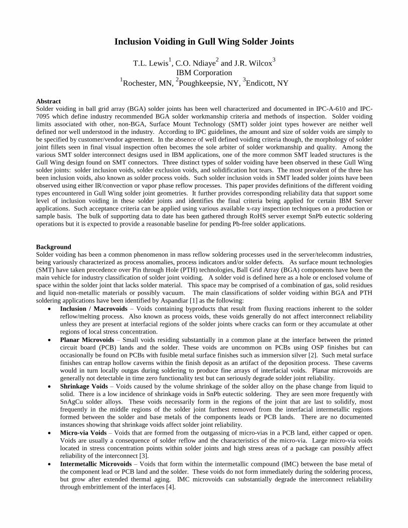
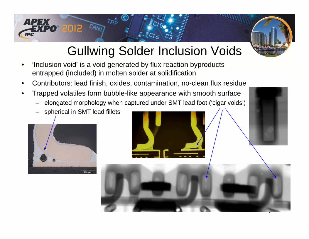
1. Inclusion Voids
The most frequently observed solder voids in leaded SMT array connectors are inclusion voids. Similar to BGA process
voids, these gull-wing inclusion voids are large macrovoids generated by flux reaction byproducts entrapped in molten
solder. Solder inclusion voids are a long recognized, and virtually unavoidable, consequence of SMT solder paste assembly.
Most entrap fully activated, no-clean flux residues. In gull-wing SMT joints, these voids range in shape from roughly
spherical to highly elongated (cigar shaped) morphologies. All have a bubble-like appearance with smooth walled surfaces.
Figure 1 shows several examples of inclusion voids in gull-wing solder joints.
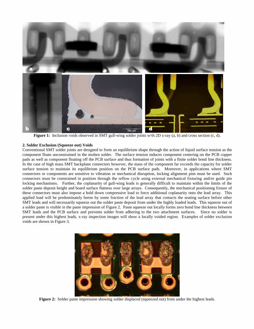
Figure 1: Inclusion voids observed in SMT gull-wing solder joints with 2D x-ray (a, b) and cross section (c, d).
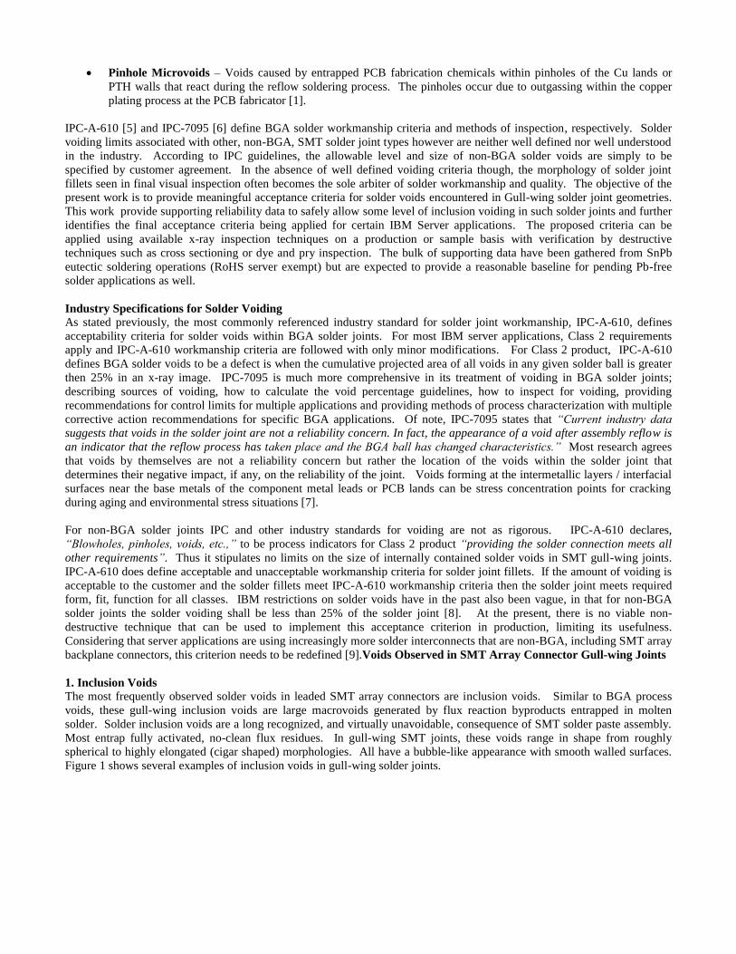
2. Solder Exclusion (Squeeze out) Voids Conventional SMT solder joints are designed to form an equilibrium shape through the action of liquid surface tension as the
component floats unconstrained in the molten solder. The surface tension induces component centering on the PCB copper
pads as well as component floating off the PCB surface and thus formation of joints with a finite solder bond line thickness.
In the case of high mass SMT backplane connectors however, the mass of the component far exceeds the capacity for solder
surface tension to maintain its equilibrium position on the PCB surface pads. Moreover, in applications where SMT
connectors or components are sensitive to vibration or mechanical disruption, locking alignment pins must be used. Such
connectors must be constrained in position through the reflow cycle using external mechanical fixturing and/or guide pin
locking mechanisms. Further, the coplanarity of gull-wing leads is generally difficult to maintain within the limits of the
solder paste deposit height and board surface flatness over large arrays. Consequently, the mechanical positioning fixture of
these connectors must also impose a hold down compressive load to force additional coplanarity onto the lead array. This
applied load will be predominately borne by some fraction of the lead array that contacts the seating surface before other
SMT leads and will necessarily squeeze out the solder paste deposit from under the highly loaded leads. This squeeze out of
a solder paste is visible in the paste impression of Figure 2. Paste squeeze out locally forms zero bond line thickness between
SMT leads and the PCB surface and prevents solder from adhering to the two attachment surfaces. Since no solder is
present under this highest leads, x-ray inspection images will show a locally voided region. Examples of solder exclusion
voids are shown in Figure 3.
Figure 2: Solder paste impression showing solder displaced (squeezed out) from under the highest leads.
aa
bb cc
aa
dd
aa
Figure 3: Solder Exclusion Voids found in SMT Gull-wing solder joints viewed in a.) cross-section and b.) 3D x-ray scans.
3. Motion Induced Voids: Hot Tearing and Ductile Rupture
Hot tearing is a well known solidification phenomenon in the field of metal casting [10]. As the solidification front in a mass
of molten metal propagates through the melt, the front must always have access to a stable pool of liquid metal to supply the
solidification process and form a defect free solid. If that liquid supply is disrupted, the solidifying metal is starved for
material and leaves void or space in the final casting. In metal casting, the most common reason for disrupting the supply of
liquid is solidification nucleating on opposing fixed external surfaces. In the case of SMT gull-wing component soldering,
hot tearing occurs through motion and/or disturbance of the joint during solidification by outside environmental factors
and/or internal material design issues with the component. Specifically, a thermally induced dimensional instability in the
component materials or the relative displacement of individual leads accumulates as solder solidification events propagate
through a large array component. This displacement forces sufficient separation of liquid solder from solid to form a tear or
void. If the solder joint has fully solidified prior to the disruptive displacement, ductile rupture may occur in the solder at
some high homologous temperature just below the melting point. Either mechanism produces a solder defect beneath the
lead foot. One should note that often the solder fillets are still visually maintained during such tearing or rupture events.
Examples of motion induced voids are shown in Figure 4.
Figure 4: Motion induced (ductile rupture) voids found in SMT gull-wing solder joints using a.) cross-section and
b.) 3D x-ray scans.
Other types of solder joint voiding not observed in the present array connector application, and hence not discussed here,
include microvia induced voids and interfacial microvoiding phenomena such as planar microvoiding from surface finish
reactions [2] and Kirkendall-like solid state voiding in the Cu3Sn intermetallic [4].
Gull-wing Solder Process Void Experience
The high density area array gull-wing SMT connector of interest is used in a range of enterprise server class products
assembled at various manufacturing sites. While the bulk of assembly production to date has used SnPb eutectic solder,
Inclusion void in heel fillet
Exclusion void under signal lead
bb aa
bb aa
several Pb-free solder applications have recently been qualified (e.g., [11]). Depending on the thermal masses involved,
some are reflowed with conventional forced convection reflow while others must use a vapor phase reflow process to
accommodate the very high thermal mass of the connector assembly. Despite this manufacturing variety, occurrences of
solder inclusion (or process) voids have been observed in all cases.
Solder inclusion voids are found in both header and receptacle backplane connectors, each of which use fundamentally
similar copper lead geometries. Because of the obscuring mass of the receptacle connector body, voids tend to be more
readily observed in x-ray inspection of the header connectors. It may also be that the receptacle wafers can exhibit more
temperature induced movement (distortion) during reflow and may thus be less likely to capture stagnant voids of process
gasses under the leads.
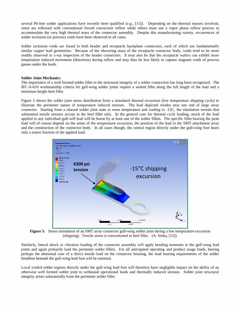
Solder Joint Mechanics
The importance of a well formed solder fillet to the structural integrity of a solder connection has long been recognized. The
IPC-A-610 workmanship criteria for gull-wing solder joints require a wetted fillet along the full length of the lead and a
minimum height heel fillet.
Figure 5 shows the solder joint stress distribution from a simulated thermal excursion (low temperature shipping cycle) to
illustrate the perimeter nature of temperature induced stresses. The lead depicted resides near one end of large array
connector. Starting from a relaxed solder joint state at room temperature and cooling to -15C, the simulation reveals that
substantial tensile stresses accrue in the heel fillet only. In the general case for thermal cycle loading, much of the load
applied to any individual gull-will lead will be borne by at least one of the solder fillets. The specific fillet bearing the peak
load will of course depend on the sense of the temperature excursion, the position of the lead in the SMT attachment array
and the construction of the connector body. In all cases though, the central region directly under the gull-wing foot bears
only a minor fraction of the applied load.
Figure 5: Stress simulation of an SMT array connector gull-wing solder joint during a low temperature excursion
(shipping). Tensile stress is concentrated in heel fillet. (A. Sinha, [12]).
Similarly, lateral shock or vibration loading of the connector assembly will apply bending moments to the gull-wing lead
joints and again primarily load the perimeter solder fillets. For all anticipated operating and product usage loads, barring
perhaps the abnormal case of a direct tensile load on the connector housing, the load bearing requirements of the solder
bondline beneath the gull-wing lead foot will be minimal.
Local voided solder regions directly under the gull-wing lead foot will therefore have negligible impact on the ability of an
otherwise well formed solder joint to withstand operational loads and thermally induced stresses. Solder joint structural
integrity arises substantially from the perimeter solder fillet.
-15°C shipping excursion
6300 psi tension
Eutectic SnPb solder inclusion voids in connector gull wing solder joints have been found to nearly always coalesce into a
single, large cigar shaped void directly under the central region of the lead foot. The stress concentration associated with a
smooth walled void, located away from the high stress fillet regions, was found to be small and thus have minimal impact on
the thermal fatigue mechanisms operating in the solder fillet regions. The primary objective of the solder joint quality
specification strategy should therefore be to assure the structural integrity of the load bearing solder fillet regions.
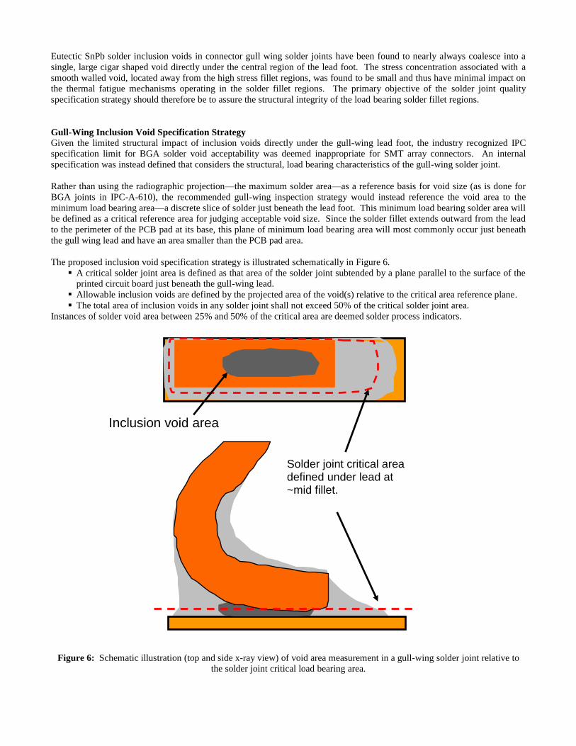
Gull-Wing Inclusion Void Specification Strategy
Given the limited structural impact of inclusion voids directly under the gull-wing lead foot, the industry recognized IPC
specification limit for BGA solder void acceptability was deemed inappropriate for SMT array connectors. An internal
specification was instead defined that considers the structural, load bearing characteristics of the gull-wing solder joint.
Rather than using the radiographic projection—the maximum solder area—as a reference basis for void size (as is done for
BGA joints in IPC-A-610), the recommended gull-wing inspection strategy would instead reference the void area to the
minimum load bearing area—a discrete slice of solder just beneath the lead foot. This minimum load bearing solder area will
be defined as a critical reference area for judging acceptable void size. Since the solder fillet extends outward from the lead
to the perimeter of the PCB pad at its base, this plane of minimum load bearing area will most commonly occur just beneath
the gull wing lead and have an area smaller than the PCB pad area.
The proposed inclusion void specification strategy is illustrated schematically in Figure 6.
A critical solder joint area is defined as that area of the solder joint subtended by a plane parallel to the surface of the
printed circuit board just beneath the gull-wing lead.
Allowable inclusion voids are defined by the projected area of the void(s) relative to the critical area reference plane.
The total area of inclusion voids in any solder joint shall not exceed 50% of the critical solder joint area.
Instances of solder void area between 25% and 50% of the critical area are deemed solder process indicators.
Figure 6: Schematic illustration (top and side x-ray view) of void area measurement in a gull-wing solder joint relative to
the solder joint critical load bearing area.
Solder joint critical area defined under lead at ~mid fillet. (under SMT lead)
Inclusion void area
This specification strategy does require a computed tomography or laminography x-ray inspection tool to capture both the
void area and the critical solder joint cross-section area beneath the gull-wing lead. Such tools are now commonly used in
the production of complex server board assemblies. They can be programmed to produce an x-ray image slice under the gull-
wing lead and calculate relative void areas in real time for 100% coverage of production solder joints if desired.
Note that it is not necessary to explicitly specify the allowable inclusion void location. Process voids forming in the lead
fillets readily escape to the free surface before solidification, leaving only those voids directly under the lead foot. Inclusion
voids in the structurally important side or toe fillets are rare and always small. Instances of small spherical inclusion voids in
the heel fillet are not uncommon but generally they occur above the plane of the defined critical load bearing area. If they are
found to intersect the critical reference plane there are should be summed and factored into the acceptability decision.
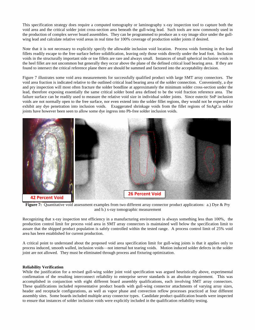
Figure 7 illustrates some void area measurements for successfully qualified product with large SMT array connectors. The
void area fraction is indicated relative to the outlined critical load bearing area of the solder connection. Conveniently, a dye
and pry inspection will most often fracture the solder bondline at approximately the minimum solder cross-section under the
lead, therefore exposing essentially the same critical solder bond area defined to be the void fraction reference area. The
failure surface can be readily used to measure the relative void size in individual solder joints. Since eutectic SnP inclusion
voids are not normally open to the free surface, nor even extend into the solder fillet regions, they would not be expected to
exhibit any dye penetration into inclusion voids. Exaggerated shrinkage voids from the fillet regions of SnAgCu solder
joints have however been seen to allow some dye ingress into Pb-free solder inclusion voids.
Figure 7: Quantitative void assessment examples from two different array connector product applications: a.) Dye & Pry
and b.) x-ray tomographic measurement
Recognizing that x-ray inspection test efficiency in a manufacturing environment is always something less than 100%, the
production control limit for process void area in SMT array connectors is maintained well below the specification limit to
assure that the shipped product population is safely controlled within the tested range. A process control limit of 25% void
area has been established for current production.
A critical point to understand about the proposed void area specification limit for gull-wing joints is that it applies only to
process induced, smooth walled, inclusion voids—not internal hot tearing voids. Motion induced solder defects in the solder
joint are not allowed. They must be eliminated through process and fixturing optimization.
Reliability Verification
While the justification for a revised gull-wing solder joint void specification was argued heuristically above, experimental
confirmation of the resulting interconnect reliability to enterprise server standards is an absolute requirement. This was
accomplished in conjunction with eight different board assembly qualifications, each involving SMT array connectors.
These qualifications included representative product boards with gull-wing connector attachments of varying array sizes,
header and receptacle configurations, as well as vapor phase and convection reflow processes practiced at four different
assembly sites. Some boards included multiple array connector types. Candidate product qualification boards were inspected
to ensure that instances of solder inclusion voids were explicitly included in the qualification reliability testing.
26 Percent Void 42 Percent Void
Solder inclusion voids were confirmed in the various connector gull-wing joints of each product qualification sample with
void areas measuring up to 50% of the critical reference area. Most of were of the elongated cigar shape morphology. All
were in SnPb eutectic solder.
Board assembly qualification for server class product includes a suite of reliability tests on representative product boards. The
primary test for establishing wear out characteristics of solder joints is the Accelerated Thermal Cycle test. ATC was
therefore the primary means of validation for the gull-wing solder inclusion void specification.
Translating ATC test results to acceptable field life is generally done with an equation of the form proposed by Norris and
Landzberg [13]. Solder fatigue life is expressed in the form of a stress test Acceleration Factor (AF); the ratio of field life to
laboratory test life. The equation is comprised of three terms, each a ratio of laboratory conditions to field conditions: a
temperature induced strain term, a cyclic frequency term, and a thermal activation term. Writing the thermal activation term
in the classic Arrehenius form, where k ≡ Boltzmann’s constant, the Norris-Landzberg equation becomes:
T refers to the cyclic temperature range (maximum – minimum), ƒ is the cyclic frequency, and T is the peak cyclic dwell
temperature. The subscripts t and 0 indicate laboratory test conditions and field conditions, respectively.
This simplified form assumes isothermal temperature distribution in the assembly, i.e., no temperature differences between
components and board. This would generally be the case for assembled boards thermal cycling in a laboratory chamber. The
ratio of approximate interconnect strains then simplifies to a ratio of cyclic temperature ranges.
The activation energy for thermal cycle fatigue damage of solder joints, Ea, has been experimentally observed to depend on
solder alloy and perhaps package structure. For SnPb eutectic solder, the activation energy has been shown to be 0.12 eV
[14]. The SMT array connectors of interest are used exclusively in enterprise server applications where the target field life
for product qualifications is 1250 power On/Off cycles. In a typical server installation, the power On cycle may drive a
35°C board temperature increase above 25°C ambient (T0=35°C, T0=60°C). These parameters are used to calculate the
minimum laboratory cycling exposure to assure the required field reliability.
Table 1 lists two examples qualification cases to illustrate the method. In each case, at least 30% of the SMT lead population
was confirmed to have some level of inclusion solder voiding in the gull-wing solder joints. Key qualification attributes are
listed. In Case 1 for instance, five functional boards were subjected ATC test with a temperature cycle of 10 to 70 °C at 1
cycle per hour. Each board contained multiple SMT array connectors for a total of 20160 tested leads per board. Using the
modified Norris-Landzberg equation above, the minimum number stress cycles to meet server reliability requirements was
calculated to be 561 cycles. All five boards completed 1000 cycles of ATC testing and remained electrically functional as
tested through the SMT connectors. In Case 2, six functional boards completed an ATC test with a temperature cycle of 0 to
100 °C at 1 cycle per hour. Each board contained two SMT connectors with total of 1968 SMT leads per board. The
minimum number of stress cycles to meet server reliability requirements was calculated to be 112 cycles. All six boards
completed 1000 cycles of ATC testing and again tested to be electrically functional through the connectors. The proposed
specification criterion for gull-wing inclusion voids was therefore confirmed with a comfortable level of conservatism; from
~2X to 9X the required ATC testing lifetimes without detectable reliability consequences.
Table 1: Two Cases of array connector Gull-wing joints with Solder Inclusion Voids subjected to ATC Reliability Testing
Case
Number of
Functional
Boards
Number of
SMT Leads
per Board
Tt
(°C)
Tt
(°C)
Acceleration
Factor
Cycles per
Hour
Minimum
ATC Cycles
Required
Cycles
Tested
(PASS)
1 5 20160 70 60 2.2 1 561 1000
2 6 1968 100 100 11 1 112 1000
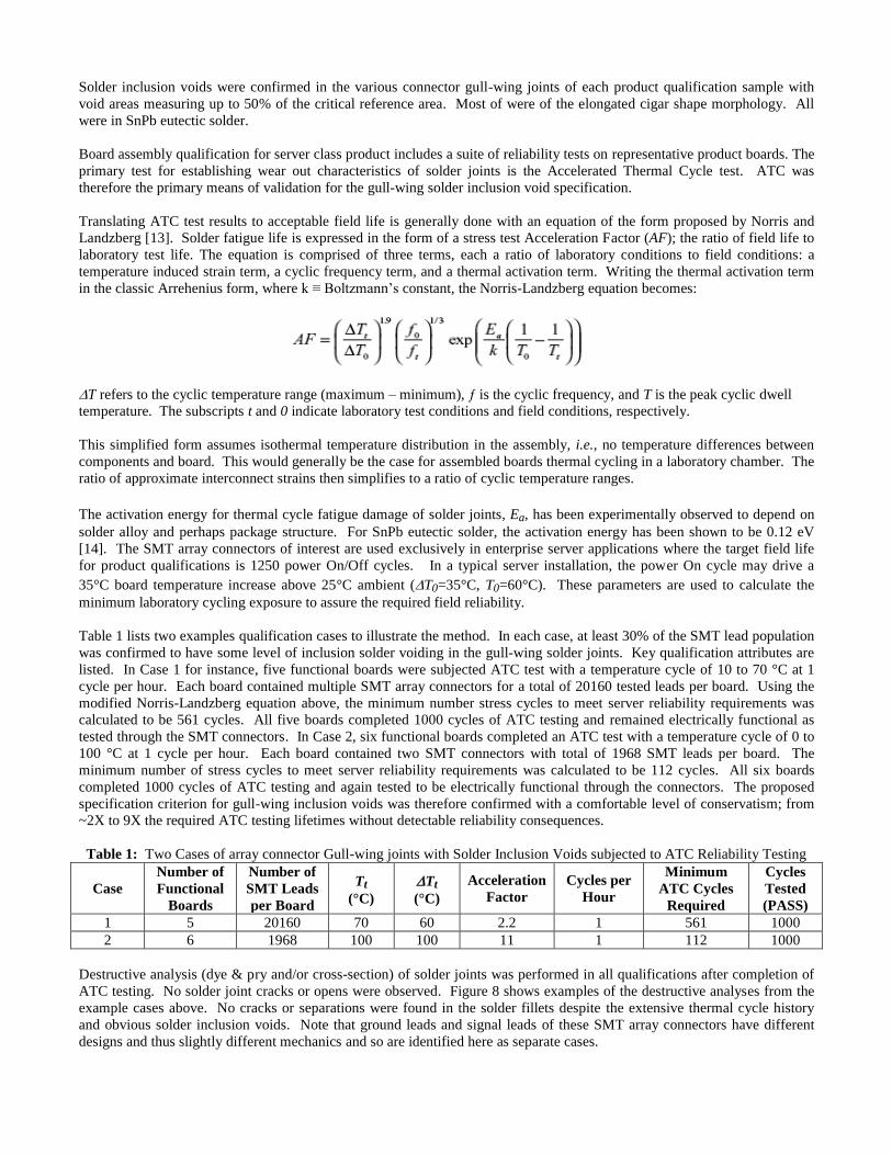
Destructive analysis (dye & pry and/or cross-section) of solder joints was performed in all qualifications after completion of
ATC testing. No solder joint cracks or opens were observed. Figure 8 shows examples of the destructive analyses from the
example cases above. No cracks or separations were found in the solder fillets despite the extensive thermal cycle history
and obvious solder inclusion voids. Note that ground leads and signal leads of these SMT array connectors have different
designs and thus slightly different mechanics and so are identified here as separate cases.
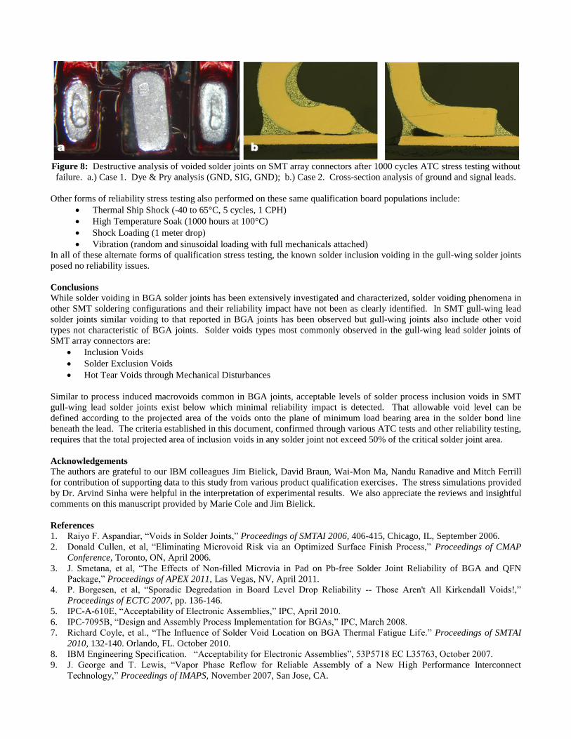
Figure 8: Destructive analysis of voided solder joints on SMT array connectors after 1000 cycles ATC stress testing without
failure. a.) Case 1. Dye & Pry analysis (GND, SIG, GND); b.) Case 2. Cross-section analysis of ground and signal leads.
Other forms of reliability stress testing also performed on these same qualification board populations include:
Thermal Ship Shock (-40 to 65°C, 5 cycles, 1 CPH)
High Temperature Soak (1000 hours at 100°C)
Shock Loading (1 meter drop)
Vibration (random and sinusoidal loading with full mechanicals attached)
In all of these alternate forms of qualification stress testing, the known solder inclusion voiding in the gull-wing solder joints
posed no reliability issues.
Conclusions
While solder voiding in BGA solder joints has been extensively investigated and characterized, solder voiding phenomena in
other SMT soldering configurations and their reliability impact have not been as clearly identified. In SMT gull-wing lead
solder joints similar voiding to that reported in BGA joints has been observed but gull-wing joints also include other void
types not characteristic of BGA joints. Solder voids types most commonly observed in the gull-wing lead solder joints of
SMT array connectors are:
Inclusion Voids
Solder Exclusion Voids
Hot Tear Voids through Mechanical Disturbances
Similar to process induced macrovoids common in BGA joints, acceptable levels of solder process inclusion voids in SMT
gull-wing lead solder joints exist below which minimal reliability impact is detected. That allowable void level can be
defined according to the projected area of the voids onto the plane of minimum load bearing area in the solder bond line
beneath the lead. The criteria established in this document, confirmed through various ATC tests and other reliability testing,
requires that the total projected area of inclusion voids in any solder joint not exceed 50% of the critical solder joint area.
Acknowledgements
The authors are grateful to our IBM colleagues Jim Bielick, David Braun, Wai-Mon Ma, Nandu Ranadive and Mitch Ferrill
for contribution of supporting data to this study from various product qualification exercises. The stress simulations provided
by Dr. Arvind Sinha were helpful in the interpretation of experimental results. We also appreciate the reviews and insightful
comments on this manuscript provided by Marie Cole and Jim Bielick.
References
1. Raiyo F. Aspandiar, “Voids in Solder Joints,” Proceedings of SMTAI 2006, 406-415, Chicago, IL, September 2006.
2. Donald Cullen, et al, “Eliminating Microvoid Risk via an Optimized Surface Finish Process,” Proceedings of CMAP
Conference, Toronto, ON, April 2006.
3. J. Smetana, et al, “The Effects of Non-filled Microvia in Pad on Pb-free Solder Joint Reliability of BGA and QFN
Package,” Proceedings of APEX 2011, Las Vegas, NV, April 2011.
4. P. Borgesen, et al, “Sporadic Degredation in Board Level Drop Reliability -- Those Aren't All Kirkendall Voids!,”
Proceedings of ECTC 2007, pp. 136-146.
5. IPC-A-610E, “Acceptability of Electronic Assemblies,” IPC, April 2010.
6. IPC-7095B, “Design and Assembly Process Implementation for BGAs,” IPC, March 2008.
7. Richard Coyle, et al., “The Influence of Solder Void Location on BGA Thermal Fatigue Life.” Proceedings of SMTAI
2010, 132-140. Orlando, FL. October 2010.
8. IBM Engineering Specification. “Acceptability for Electronic Assemblies”, 53P5718 EC L35763, October 2007.
9. J. George and T. Lewis, “Vapor Phase Reflow for Reliable Assembly of a New High Performance Interconnect
Technology,” Proceedings of IMAPS, November 2007, San Jose, CA.
aa bb
10. M.C. Flemings, Solidification Processing, McGraw-Hill, 1974, pp.253-256.
11. PK Pu, et al, “Lead-Free Solder Assembly Implementation for a Mid-Range Power Systems Server,” Proceedings of
SMTAI” 2011, 581-588, Ft. Worth, TX, October 2011.
12. Arvind Sinha, IBM S&TG Development, private communication.
13. K.C. Norris and A.H. Landzberg, IBM Journal of Research and Development. Vol. 13, May 1969, pp. 266-271.
14. IBM Engineering Specification. “IBM Specification for Printed Circuit Board Assembly (PCBA) Reliability Tests”,
0871889 EC L35590, July 2007.
Inclusion Voiding in Gullwing Solder JointsIBM Corporation
Theron Lewis, Jim Wilcox, Cheikhou O. Ndiaye
[email protected] CorporationRochester, MN
Agenda
• Introduction / Objectives
• Solder Voiding Criteria
• Solder Voiding in Gullwing Joints
• Solder Inclusion Void Criterion
• Reliability Verification
• Summary and Conclusions
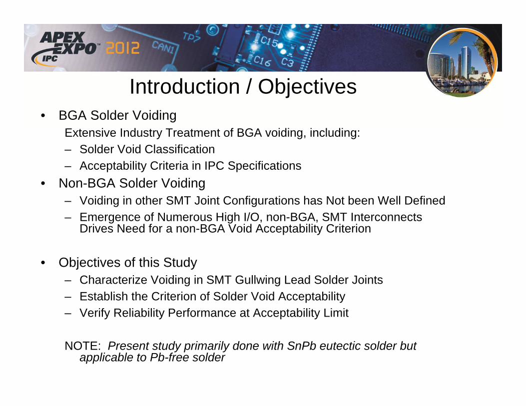
Introduction / Objectives• BGA Solder Voiding
Extensive Industry Treatment of BGA voiding, including:– Solder Void Classification– Acceptability Criteria in IPC Specifications
• Non-BGA Solder Voiding – Voiding in other SMT Joint Configurations has Not been Well Defined– Emergence of Numerous High I/O, non-BGA, SMT Interconnects
Drives Need for a non-BGA Void Acceptability Criterion
• Objectives of this Study– Characterize Voiding in SMT Gullwing Lead Solder Joints– Establish the Criterion of Solder Void Acceptability– Verify Reliability Performance at Acceptability Limit
NOTE: Present study primarily done with SnPb eutectic solder but applicable to Pb-free solder
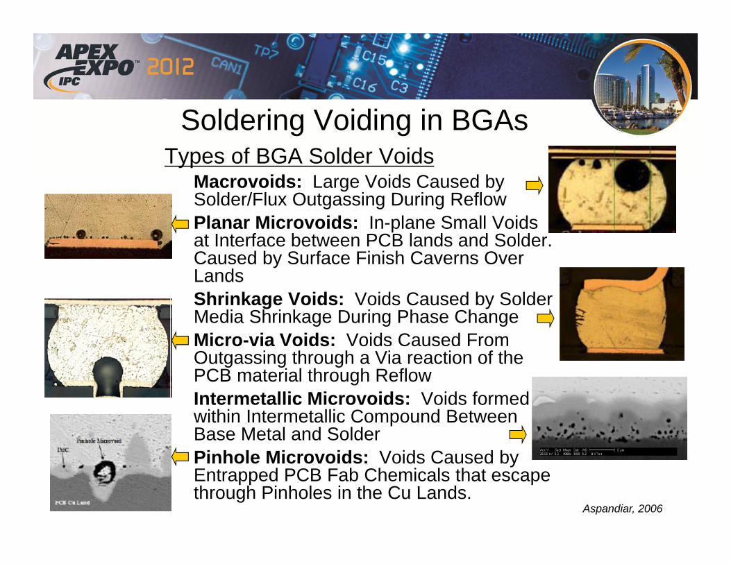
Soldering Voiding in BGAsTypes of BGA Solder Voids– Macrovoids: Large Voids Caused by
Solder/Flux Outgassing During Reflow– Planar Microvoids: In-plane Small Voids
at Interface between PCB lands and Solder. Caused by Surface Finish Caverns Over Lands
– Shrinkage Voids: Voids Caused by Solder Media Shrinkage During Phase Change
– Micro-via Voids: Voids Caused From Outgassing through a Via reaction of the PCB material through Reflow
– Intermetallic Microvoids: Voids formed within Intermetallic Compound Between Base Metal and Solder
– Pinhole Microvoids: Voids Caused by Entrapped PCB Fab Chemicals that escape through Pinholes in the Cu Lands.
Aspandiar, 2006

Solder Voiding Criteria• Most Server Applications follow IPC Class 2 Requirements• IPC-A-610 (Class 2)
– BGA joint: Solder ball with cumulative area of voids greater than 25% area of x-ray image constitutes a defect.
– Non-BGA joint: “Blowholes, pinholes, voids, etc.,” are Process Indicators “providing the solder connection meets all other requirements.”
• IPC-7095– More comprehensive treatment of BGA solder voiding, including
• Common sources of voiding • Inspection, Analysis and Classification of Solder Voids• Recommendations for control limits in multiple applications • Methods of process characterization with recommended corrective actions.
– “Current industry data suggests that voids in the solder joint are not a reliability concern. In fact, the appearance of a void after assembly reflow is an indicator that the reflow process has taken place and the BGA ball has changed characteristics.”
– Other research has shown voids at the intermetallic layers / interfaces can be stress concentration points for cracking during environmental stress situations.
• Legacy Internal Engineering Specification– Solder voiding shall be less than 25% of the solder joint volume.– Non-destructive technique to implement in a production environment not available.
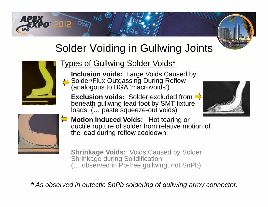
Solder Voiding in Gullwing JointsTypes of Gullwing Solder Voids*– Inclusion voids: Large Voids Caused by
Solder/Flux Outgassing During Reflow(analogous to BGA ‘macrovoids’)
– Exclusion voids: Solder excluded from beneath gullwing lead foot by SMT fixture loads (… paste squeeze-out voids)
– Motion Induced Voids: Hot tearing or ductile rupture of solder from relative motion of the lead during reflow cooldown.
– Shrinkage Voids: Voids Caused by Solder Shrinkage during Solidification(… observed in Pb-free gullwing; not SnPb)
–* As observed in eutectic SnPb soldering of gullwing array connector.
7
Gullwing Solder Inclusion Voids• ‘Inclusion void’ is a void generated by flux reaction byproducts
entrapped (included) in molten solder at solidification• Contributors: lead finish, oxides, contamination, no-clean flux residue• Trapped volatiles form bubble-like appearance with smooth surface
– elongated morphology when captured under SMT lead foot (‘cigar voids’)– spherical in SMT lead fillets
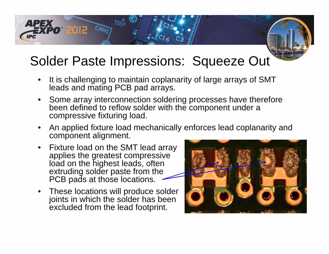
Solder Paste Impressions: Squeeze Out• It is challenging to maintain coplanarity of large arrays of SMT
leads and mating PCB pad arrays. • Some array interconnection soldering processes have therefore
been defined to reflow solder with the component under a compressive fixturing load.
• An applied fixture load mechanically enforces lead coplanarity and component alignment.
• Fixture load on the SMT lead array applies the greatest compressive load on the highest leads, often extruding solder paste from the PCB pads at those locations.
• These locations will produce solder joints in which the solder has been excluded from the lead footprint.
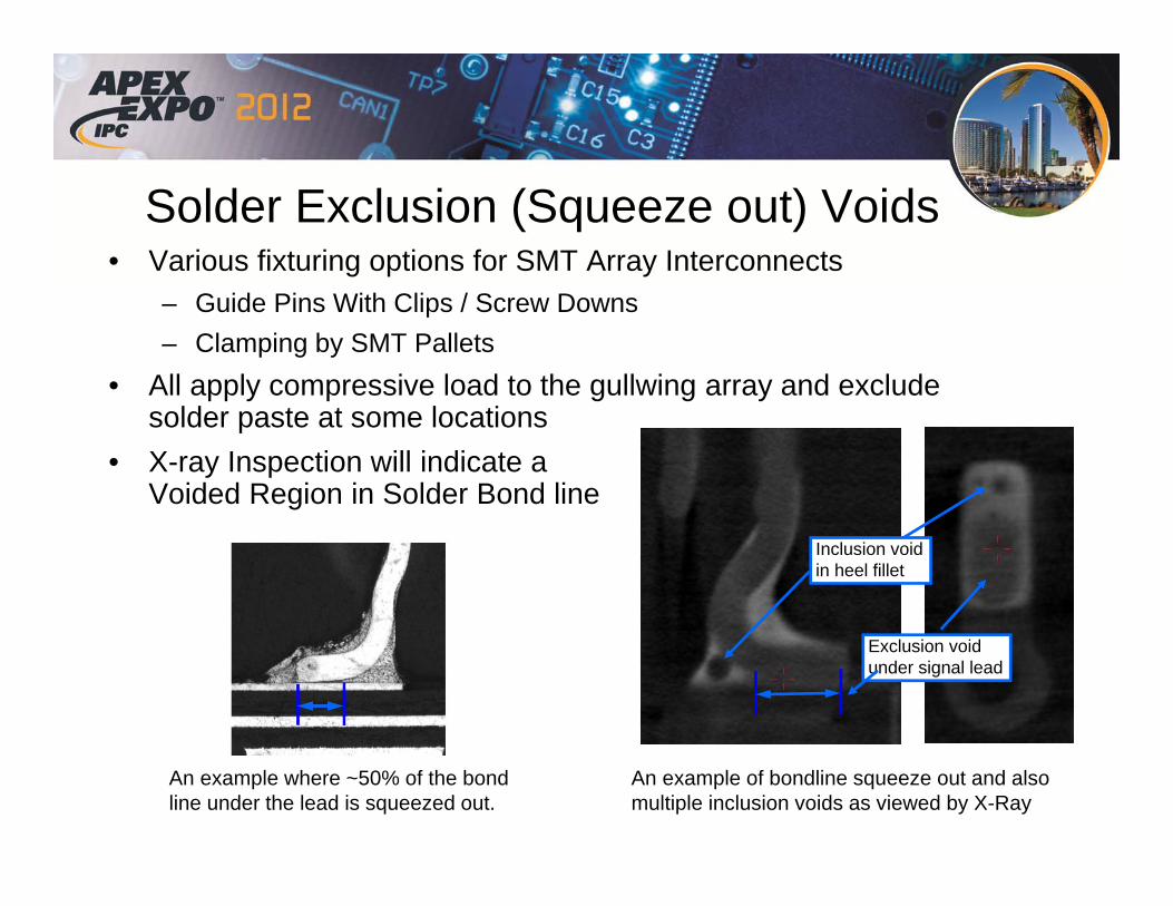
Solder Exclusion (Squeeze out) Voids• Various fixturing options for SMT Array Interconnects
– Guide Pins With Clips / Screw Downs– Clamping by SMT Pallets
• All apply compressive load to the gullwing array and exclude solder paste at some locations
• X-ray Inspection will indicate a Voided Region in Solder Bond line
An example where ~50% of the bond line under the lead is squeezed out.
An example of bondline squeeze out and also multiple inclusion voids as viewed by X-Ray
Inclusion void in heel fillet
Exclusion void under signal lead
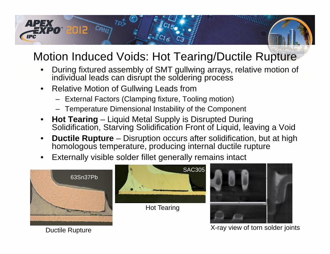
Motion Induced Voids: Hot Tearing/Ductile Rupture• During fixtured assembly of SMT gullwing arrays, relative motion of
individual leads can disrupt the soldering process• Relative Motion of Gullwing Leads from
– External Factors (Clamping fixture, Tooling motion)– Temperature Dimensional Instability of the Component
• Hot Tearing – Liquid Metal Supply is Disrupted During Solidification, Starving Solidification Front of Liquid, leaving a Void
• Ductile Rupture – Disruption occurs after solidification, but at high homologous temperature, producing internal ductile rupture
• Externally visible solder fillet generally remains intact
Ductile Rupture
Hot Tearing
SAC30563Sn37Pb
X-ray view of torn solder joints
Gullwing Process Void Experience • Typical Gullwing SMT Leaded Components
– QFPs– TSOPs– SMT Electrolytic Caps– Other Components
• High Density Area Array Connectors– Replaced PTH Connectors– Up to 5040 I/O SMT Leads– Due to Mating/Plugging of Cards, Solder Joints can be Under Tensile and/or
Compression Forces– Have Put Renewed Focus On Solder Joint Quality
• Solder Inclusion Voiding– Despite Variety of Manufacturing Methods and Paste Chemistry, Inclusion Voids
can be Found in all Classes– Occurs in Vapor Phase Reflow or Convection Reflow– Occurs in Pb Free Solder or SnPb Eutectic Solder
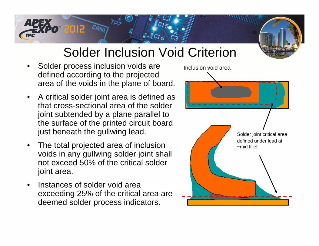
Solder Inclusion Void CriterionInclusion void area
Solder joint critical areadefined under lead at ~mid fillet
• Solder process inclusion voids are defined according to the projected area of the voids in the plane of board.
• A critical solder joint area is defined as that cross-sectional area of the solder joint subtended by a plane parallel to the surface of the printed circuit board just beneath the gullwing lead.
• The total projected area of inclusion voids in any gullwing solder joint shall not exceed 50% of the critical solder joint area.
• Instances of solder void area exceeding 25% of the critical area are deemed solder process indicators.
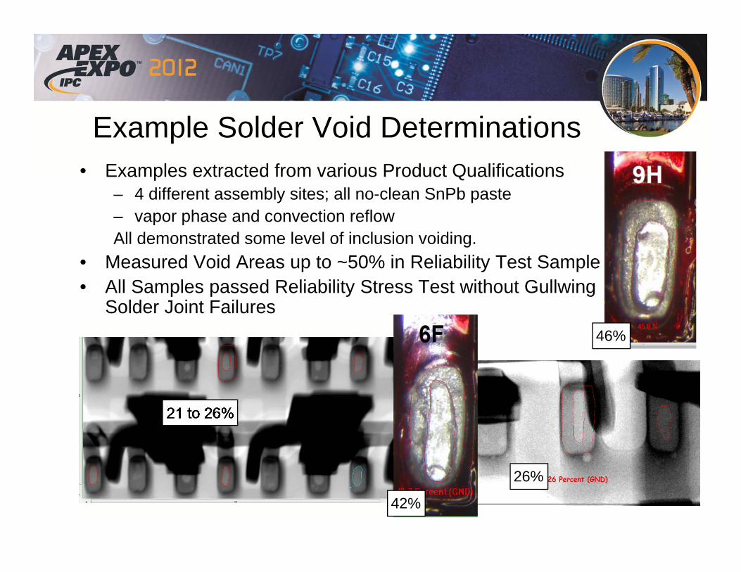
Example Solder Void Determinations• Examples extracted from various Product Qualifications
– 4 different assembly sites; all no-clean SnPb paste– vapor phase and convection reflowAll demonstrated some level of inclusion voiding.
• Measured Void Areas up to ~50% in Reliability Test Sample• All Samples passed Reliability Stress Test without Gullwing
Solder Joint Failures
26%
46%
42%
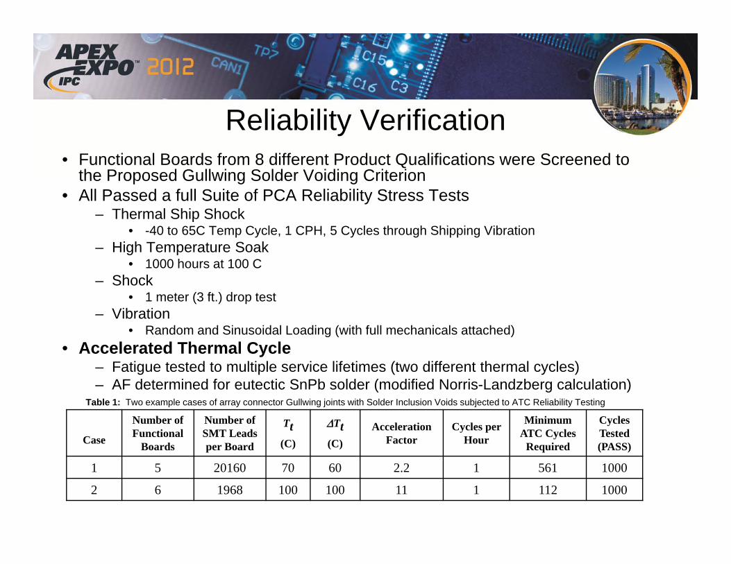
Reliability Verification• Functional Boards from 8 different Product Qualifications were Screened to
the Proposed Gullwing Solder Voiding Criterion • All Passed a full Suite of PCA Reliability Stress Tests
– Thermal Ship Shock• -40 to 65C Temp Cycle, 1 CPH, 5 Cycles through Shipping Vibration
– High Temperature Soak• 1000 hours at 100 C
– Shock• 1 meter (3 ft.) drop test
– Vibration• Random and Sinusoidal Loading (with full mechanicals attached)
• Accelerated Thermal Cycle – Fatigue tested to multiple service lifetimes (two different thermal cycles) – AF determined for eutectic SnPb solder (modified Norris-Landzberg calculation)
Table 1: Two example cases of array connector Gullwing joints with Solder Inclusion Voids subjected to ATC Reliability Testing
Case
Number of Functional
Boards
Number of SMT Leads per Board
Tt (C)
Tt (C)
AccelerationFactor
Cycles per Hour
Minimum ATC Cycles
Required
Cycles Tested (PASS)
1 5 20160 70 60 2.2 1 561 1000
2 6 1968 100 100 11 1 112 1000
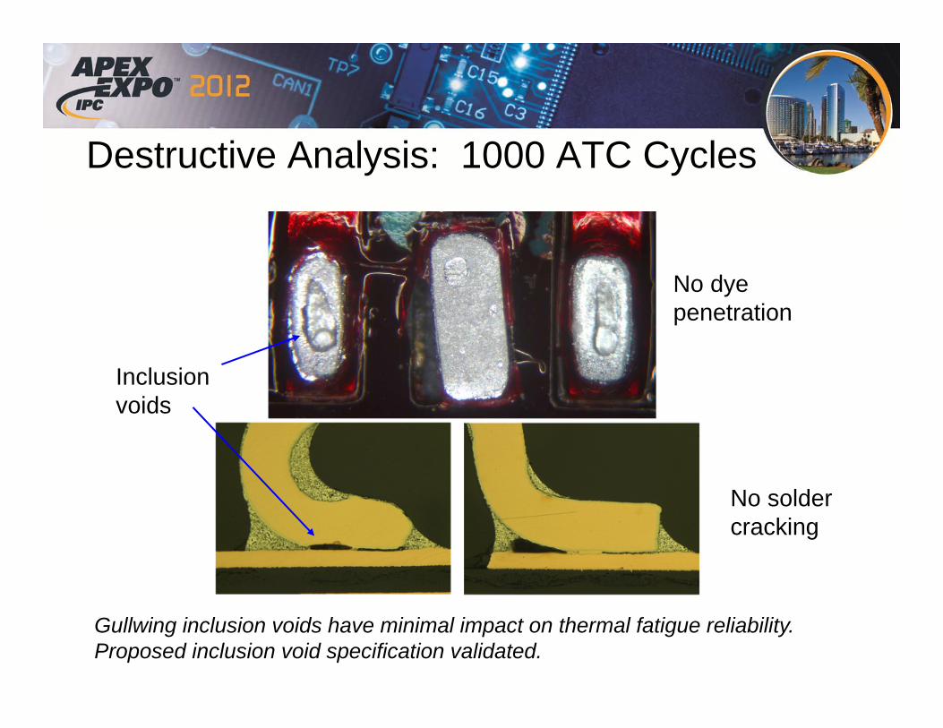
Destructive Analysis: 1000 ATC Cycles
No dye penetration
No solder cracking
Inclusion voids
Gullwing inclusion voids have minimal impact on thermal fatigue reliability. Proposed inclusion void specification validated.
Summary and Conclusions• BGA Solder Voiding has been Extensively Investigated and Characterized.• Current Industry Guidelines Regarding Solder Inclusion Voids are Vague for
Non-BGA SMT Components. – Voiding Behavior is not well Defined in other SMT Solder Joint Configurations
• Most Common Type of Voids Observed in Gullwing Lead Solder Joints:– Solder Inclusion Voids– Solder Exclusion Voids– Motion Induced Hot Tearing or Ductile Rupture
• A Workable Criterion Has been Established for Inclusion Voids in Gullwing Leaded SMT Joints Relative to a Critical Load Bearing Area
– Total projected area of inclusion voids in gullwing solder joint shall not exceed 50% of the critical solder joint area
• Multiple Assembly Qualifications have Validated this Acceptability Limit for Gullwing Inclusion Voids through Reliability Testing.
– Structural Integrity of Gullwing Solder Fillets are Not Affected by Inclusion Voids– Voided Joints can still Meet the Reliability, Form, Fit, and Function Required

Acknowledgements
• The authors are grateful to our IBM colleagues for technical data contributions to this study– Jim Bielick – Wai-Mon Ma – Mitch Ferrill– David Braun – Nandu Ranadive – Phil Isaacs
• Stress simulations provided by Dr. Arvind Sinha were helpful in the interpretation of experimental results.
• We also appreciate reviews and insightful comments on this manuscript provided by – Jim Bielick – Marie Cole