In situ TEM Observation of Cu-Sn Soldering v4.docx
28
1 In Situ Visualization of Metallurgical Reactions in Nanoscale Cu/Sn Diffusion Couples 1 Qiyue Yin 1 , Fan Gao 2 , Zhiyong Gu 2 , Eric A. Stach 3 , Guangwen Zhou 1 2 1 Department of Mechanical Engineering & Multidisciplinary Program in Materials Science and 3 Engineering, State University of New York at Binghamton, NY 13902 4 2 Department of Chemical Engineering, University of Massachusetts Lowell, Lowell, MA 01854 5 3 Center for functional Nanomaterials, Brookhaven National Laboratory, Upton, NY 11973 6 7 Abstract 8 The Cu-Sn metallurgical soldering reaction in two-segmented Cu-Sn nanowires is visualized in real 9 time using in-situ transmission electron microscopy. By varying the relative lengths of Cu and Sn 10 segments, we show that the metallurgical reaction starts at ~ 200 °C with the formation of a Cu-Sn 11 solid solution for the Sn/Cu length ratio smaller than 1:5 while the formation of Cu-Sn intermetallic 12 compounds (IMC) for larger Sn/Cu length ratios. Upon heating the nanowires up to ~ 500 °C, two 13 phase transformation pathways occur, η-Cu 6 Sn 5 → ε-Cu 3 Sn → δ-Cu 41 Sn 11 for nanowires with a long 14 Cu segment and η-Cu 6 Sn 5 → ε-Cu 3 Sn → γ-Cu 3 Sn with a short Cu segment. The dynamic in situ TEM 15 visualization of the evolution of Kirkendall voids demonstrates that Cu diffuses faster both in Sn and 16 IMCs than that of Sn in Cu and IMCs, which is the underlying cause of the dependence of the IMC 17 formation and associated phase evolution on the relative lengths of the Cu and Sn segments. 18 19 20 *To whom correspondence should be addressed. Email: [email protected] 21 22 BNL-108171-2015-JA
Transcript of In situ TEM Observation of Cu-Sn Soldering v4.docx

1
In Situ Visualization of Metallurgical Reactions in Nanoscale Cu/Sn Diffusion Couples 1
Qiyue Yin1, Fan Gao
2, Zhiyong Gu
2, Eric A. Stach
3, Guangwen Zhou
1 2
1Department of Mechanical Engineering & Multidisciplinary Program in Materials Science and 3
Engineering, State University of New York at Binghamton, NY 13902 4
2Department of Chemical Engineering, University of Massachusetts Lowell, Lowell, MA 01854 5
3Center for functional Nanomaterials, Brookhaven National Laboratory, Upton, NY 11973 6
7
Abstract 8
The Cu-Sn metallurgical soldering reaction in two-segmented Cu-Sn nanowires is visualized in real 9
time using in-situ transmission electron microscopy. By varying the relative lengths of Cu and Sn 10
segments, we show that the metallurgical reaction starts at ~ 200 °C with the formation of a Cu-Sn 11
solid solution for the Sn/Cu length ratio smaller than 1:5 while the formation of Cu-Sn intermetallic 12
compounds (IMC) for larger Sn/Cu length ratios. Upon heating the nanowires up to ~ 500 °C, two 13
phase transformation pathways occur, η-Cu6Sn5 → ε-Cu3Sn → δ-Cu41Sn11 for nanowires with a long 14
Cu segment and η-Cu6Sn5 → ε-Cu3Sn → γ-Cu3Sn with a short Cu segment. The dynamic in situ TEM 15
visualization of the evolution of Kirkendall voids demonstrates that Cu diffuses faster both in Sn and 16
IMCs than that of Sn in Cu and IMCs, which is the underlying cause of the dependence of the IMC 17
formation and associated phase evolution on the relative lengths of the Cu and Sn segments. 18
19
20
*To whom correspondence should be addressed. Email: [email protected]
22
BNL-108171-2015-JA

2
1. Introduction 1
With the development of materials synthesis and processing approaches, fabrication of well-2
defined nanostructures has become an everyday experience. A natural extension of this progress is to 3
find ways to combine nanostructures of various origins, characters, and components, which requires 4
making nanoscale contacts in these nanostructures and has become one of the main challenges in 5
nanoscale integration[1, 2]
. As an essential part of electronic circuits, lead-free (Pb-free) nano-solders 6
hold tremendous potential as a viable solution for replacing traditional tin/lead (Sn/Pb) solders which 7
have toxic properties and may be harmful for health and the environment. Pb-free nano solders also 8
offer exceptional opportunities for making nanoscale contacts as needed with the miniaturization of 9
devices as well as the production of nanosized circuits. Pb-free solders have been extensively 10
produced in bulk, powder and thin films[3-9]
. Different solder nanowires such as Sn, In, Sn-Cu, Sn-Ag, 11
have been synthesized directly using electrodeposition in nanoporous templates[10-12]
. However, the 12
knowledge of many properties of Pb-free nanosolders, including diffusion, intermetallic reaction 13
mechanisms and phase evolution is still very limited. 14
The binary copper-tin (Cu-Sn) system is one of the simplest metallurgical options for various 15
methods of the interconnection in three-dimensional (3D) integration because of their easy formation 16
of Cu-Sn intermetallic compounds (IMCs) that serve as the mechanical bonding between Sn-based 17
solder and the copper pad of a printed circuit board (PCB)[13, 14]
. The presence of a thin interfacial Cu-18
Sn IMC layer is essential for the bondability of the Cu pad because the IMC promotes good wetting 19
between solder and copper[15-20]
. Although the solid-state growth of Cu-Sn IMCs has been investigated 20
extensively, almost all the previous studies have been dealt with the bulk materials, which may differ 21
significantly from the nanoscale soldering in a number of ways owning to the size and geometrical 22
effects associated with nanosolders, including the amount of solder formed at the joint, diffusion path, 23
phase evolution of IMCs, geometry of the IMC solder joint, and formation of voids in the IMC and at 24
the joint interfaces. All these potential factors can significantly affect the growth and bondability of 25
IMC for forming stable nanoscale contacts[21-27]
. By choosing two-segment Cu-Sn nanowires as a 26

3
model system in which Sn acts as the solder element and Cu serves as a functional element, we aim to 1
understand the nanoscale metallurgical soldering reaction at temperatures up to ~ 500 °C. Although the 2
reflow temperature for typical soldering reactions normally does not go beyond 300 °C it is also of 3
fundamental interest for understanding how the IMCs such as Cu3Sn and Cu6Sn5 IMCs formed at the 4
lower temperatures evolve at high temperatures in addition to the potential applications in developing 5
the solders with high temperature tolerance. Using in-situ transmission electron microcopy (TEM) 6
observations, we elucidate the phase/structural transformation of various IMCs and its dependence on 7
length of the Sn and Cu segments as well as the formation and growth of Kirkendall voids by the 8
reactive diffusion between Cu and Sn. 9
10
11
2. Experimental 12
The Cu-Sn two-segment nanowires were fabricated by room-temperature sequential 13
electrodeposition assisted with polycarbonate nanoporous membrane templates (Whatman). Cu was 14
deposited first using a commercial Cu plating electrolyte (Cu U-bath RTU, Technic, Inc) with the 15
current controlled at 2 mA/cm2. After Cu plating, the Sn layer was electroplated by commercial Sn 16
plating electrolyte (Sn concentrate with make-up solutions, Technic, Inc.) with the current controlled 17
at 18 mA/cm2. After the electroplating, the polycarbonate membrane was dissolved in 18
dichloromethane to release the nanowires into the solvent. Details of the synthesis of the nanosolders 19
can be found from previous work[28, 29]
. The as-prepared Cu-Sn nanowires were kept as a solution in 20
ethanol. TEM samples were prepared by the powder sample preparation method with ultrasonic 21
dispersion followed with drop casting onto a lacey carbon film supported by TEM Mo grid purchased 22
from Ted Pella, which was then mounted onto a Gatan heating holder with rapid heating capability 23
using a Gatan hot-stage temperature controller. In-situ TEM observations of the soldering reaction in 24
the Cu-Sn nanowires were performed using a JEOL JEM2100F transmission electron microscope 25
operated at 200 kV. To clarify the structure of IMCs formed after heating, some of the samples was 26

4
further examined by a traditional double tilt holder after rapidly cooling the sample to room 1
temperature with a cooling rate of ~ 100 °C/min. 2
3
3. Results and Discussion 4
Cu and Sn two segments are fabricated in the form of nanowires for the soldering reaction 5
study. Fig. 1(a) shows a backscattered scanning electron microscopy (SEM) image of the as-6
synthesized Cu-Sn nanowires, where the bright segments of the nanowires correspond to the Sn-rich 7
segments while the slightly dark segments correspond to the Cu-rich segments owing to the heavier 8
atom of Sn than Cu. Fig. 1(b) shows a scanning transmission electron microscopy (STEM) bright-9
field (BF) image of an as-synthesized nanowire with the corresponding energy-dispersive X-ray 10
spectroscopy (EDS) elemental mapping shown in Figs. 1(c, d), from which the Sn and Cu segments 11
can be easily identified. The EDS mapping reveals that the Sn segment has some intensity signal of 12
Cu while the Cu segment has much less Sn signal, suggesting there is more interdiffusion of Cu into 13
the Sn segment. Quantitative spot-mode EDS analyses of the compositions of the Cu and Sn segments 14
indicate that the purity for the Cu segment is ~ 99% and the Sn segment has the purity of ~ 90%. The 15
high purityof the two segments is also confirmed by electron diffraction analysis of the nanowire. Figs. 16
1(e, f) are selected area electron diffraction (SAED) patterns obtained from the Sn and Cu segments, 17
respectively. The indexing of these patterns matches well with the crystal structures of pure Sn and Cu. 18
These compositional and structural features of the nanowires are confirmed by checking other dozens 19
of as-prepared Cu-Sn two segment nanowires. 20
To study the Cu/Sn soldering reaction, a single nanowire is selected for in-situ heating TEM 21
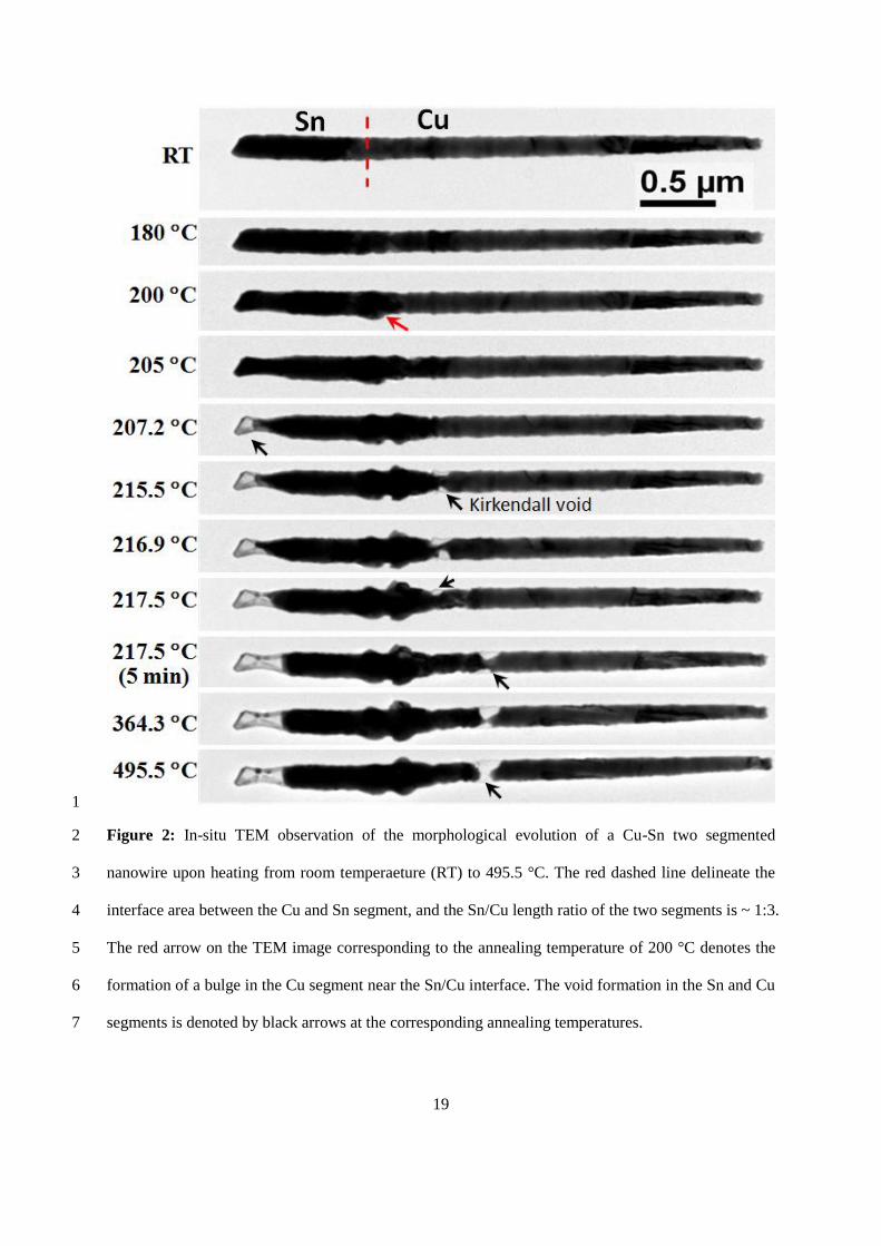
observations. Fig. 2 shows the morphological evolution of a nanowire while it is being heated from 22
room temperature (RT) to 495.5 °C with the holding time of ~ 1 min for each temperature interval 23
unless specified. The dashed line denotes the original interface region of the two segments as known 24
from the EDS analysis shown in Figs. 1(c, d, e and f), with the Sn segment on the left and the long Cu 25
segment on the right. The Sn/Cu length ratio of the two segments is about 1:3. The nanowire has no 26

5
obvious changes in morphology until it is being heated to ~ 200 °C, at which a bulge starts to become 1
visible in the Cu segment near the Sn/Cu interface. Concurrent with the bulge formation, the diameter 2
for the Sn segment near its end on the left is shrinking (see the corresponding TEM images at 200 °C 3
and 205 °C). This trend becomes more obvious as the temperature is raised to 207 °C; the TEM image 4
obtained at this temperature shows that a void is formed at the left end of the Sn segment, where the 5
outer layer of the void is a native amorphous Sn oxide layer formed from the sample preparation. 6
With further increase in temperature, the bulge grows larger with more Sn depleted from the end of 7
the Sn segment, as seen from the void growth. Meanwhile, new voids are formed in the Cu segment 8
near the bulge (see the TEM image corresponding to the temperature of 215.5 °C). The voids in the 9
Cu segment migrate away from the bulge and merge, forming a larger void with the continued 10
annealing at 217.5 °C for 5 min. Further increase in the annealing temperature to 364 °C and then to 11
495.5 °C results in the void growth that eventually leads to the breakage of the Cu segment. 12
The above in-situ TEM observation reveals that the Cu-Sn metallurgical reaction occurs 13
around 200 °C and the bulge formation around this temperature range can be attributed to the 14
formation of the IMC η-phase Cu6Sn5. As copper diffuses into tin, it forms Cu6Sn5 by 15
6Cu+5Sn→Cu6Sn5, ∆Vm=Vm (Cu6Sn5)-5Vm (Sn) = 115.28 cm3/mol -5˟16.29 cm
3/mol =33.83cm
3/mol, 16
we can tell that the combined volume of the Cu6Sn5 and the displaced tin atoms is greater than the 17
original volume of tin atoms in that space. The volume expansion results in the formation of the bulge. 18
The bulge morphology observed here also resembles the typical scallop shape of η-Cu6Sn5 observed 19
in bulk solders[21, 30-36]
. However, as seen clearly from the in-situ TEM images, the η-Cu6Sn5 bulge is 20
formed initially in the Cu segment, suggesting that Sn diffuses into the Cu segment to form the IMC. 21
This is different from the bulk soldering reaction for which the formation of η-Cu6Sn5 scallops is 22
typically attributed to the diffusion of Cu into Sn[37-43]
. However, once the IMC is formed, the reaction 23
is mainly limited to the Sn segment by Cu diffusion into Sn through the formed IMC. This is 24
evidenced by the void formation in the Cu segment near the IMC/Cu interface due to the Kirkendall 25
effect, i.e., the diffusion of Cu in the IMC is faster than that of Sn in the IMC[44, 45]
. With the 26

6
continued IMC growth, Sn is gradually consumed by reacting with incoming Cu atoms supplied by 1
solid-state diffusion of Cu through the IMC layer, which results in the void growth at the end of the 2
Sn segment. One can see that the void in the Sn segment has no noticeable change after the 3
temperature is raised above 217.5 °C and thereafter, indicating that Sn has been completely 4
consumed to form the IMC at this reaction stage. The continued growth of the Kirkendall void in the 5
Cu segment at the temperature above 217.5 °C suggests that more Cu diffuses to the reacted region to 6
form Cu-rich IMCs while the nanowire is being heated to the higher temperatures. One can also note 7
that the morphology and length of the Cu segment on the right of the Kirkendall void remains 8
unchanged during the entire annealing process, demonstrating that there is little diffusion of Sn to the 9
Cu segment due to the slower diffusion rate of Sn in the IMC than that of Cu in the IMC. 10
For pure Sn, it has been reported that the melting temperature starts to decrease when the size 11
of the nanoparticles is below 50 nm[46-48]
. The DSC profile of the pure tin nanowires with 50nm 12
diameters indicates the melting point 231.2℃ , very close to the bulk Sn. Thus we believe the 13
nanowires being studied in our study with an average diameter ~150nm have close melting point as 14
bulk Sn 231.93℃. The Gatan heating holder used for this in situ study has its temperature measured 15
by a thermocouple in contact with the cylinder furnace within about ±15K. And this temperature 16
measurement error varies with the temperature range. The measured temperature is higher than the 17
actual specimen temperature when conduction is the main thermal transfer under vaccum until 18
radiation starts to predominate at higher temperature. However, this measured melting point of Sn is 19
45℃ higher than the measured temperature 200℃ when bulging started, as shown in Fig. 2. Therefore, 20
the formation of the bulge is not caused by the melting of the Sn segment. Both the Cu-Sn 21
metallurgical reaction and the formation of voids in the Cu and Sn segments shown in Fig. 2 occurs in 22
the solid state. 23
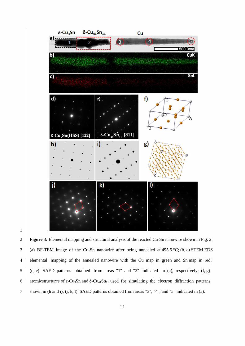
The nanowire shown in Fig. 2 was then rapidly cooled down to room temperature (cooling rate 24
~100 oC/min) from the peak temperature of 495.5 °C and the crystal structure and chemical 25

7
composition of the different regions as indicated in Fig. 3(a) of the reacted Cu-Sn solder were 1
characterized in detail by TEM. Figs. 3(b, c) are the EDS elemental maps of Cu and Sn, which show 2
high concentration of Cu in the Sn segment while still weak intensity of Sn in the Cu segment (the 3
zero drop of both Cu and Sn signals corresponds to the Kirkendall void formed between the two 4
segments). The elemental mapping is consistent with the in-situ TEM observations (Fig. 2) of the 5
morphological evolution of the soldering reaction induced mainly by Cu diffusion through the IMC to 6
react with Sn. Figs. 3(d, e) are SAED patterns obtained from region "1" and "2" indicated by the 7
dashed rectangles shown in Fig. 3(a), which reveal that area "1" is ε-Cu3Sn while area "2" is δ-8
Cu41Sn11. There is no particular orientation relationship between the two IMC phases. Figs. 3(f, g) 9
show the structure models of the hexagonal superstructure (HSS) of ε-Cu3Sn[31]
and cubic δ-10
Cu41Sn11[49]
and Figs. 3(h, i) are the simulated electron diffraction patterns of ε-Cu3Sn[122] and δ-11
Cu41Sn11[311], respectively, both of which match well with the experimental diffraction patterns 12
shown in Figs. 3(d, e). Figs. 3(j, k, l) are SAED patterns obtained from areas "3", "4", and "5" in the 13
Cu-rich segment on the right of the Kirkendall void, as indicated in Fig. 3(a). All these patterns can be 14
indexed well with the same zone axis [110] of Cu FCC structure with different in-plane rotations (i.e., 15
the Cu segment shows a texture structure aligned along [110] with multi twinning boundaries which 16
are visible in the TEM BF image shown in Fig. 3(a)). Since the Cu segment contains a small amount 17
of Sn, the structure can be regarded as α-Cu(Sn), a solid solution of Sn in Cu. In the Cu-Sn phase 18
diagram this solid solution of Sn in Cu has a composition up to 9.1 at% Sn, depending on the 19
temperature. 20
The Kikuchi lines and SAED pattern reveal that there are only ε-Cu3Sn and δ-Cu41Sn11 in the 21
reacted Sn segment, where δ-Cu41Sn11 is located adjacent to the Kirkendall void in the original Cu 22
segment and ε-Cu3Sn is located on the Sn end, as marked in Fig. 3(a) by the black dashed and red 23
rectangles, respectively. The EDS line scan along the longitudinal direction of the nanowire gives 24
three different Sn atomic compositions, 27.0%, 21.1% , 8.5%, which correspond to area 1(ε-Cu3Sn), 25
area 2 (δ-Cu41Sn11), and area 3 (α-Cu), respectively. .According to the Cu-Sn phase equilibrium, δ-26

8
Cu41Sn11 is a thermodynamically stable phase ranging from 350 to 590 °C [50, 51]
, which is formed by 1
consuming the ε-Cu3Sn phase formed at the lower temperature with Cu supplied from the Cu segment 2
as the reaction temperature is raised above 217 °C, as shown in Fig. 2. The absence of the η-Cu6Sn5 3
phase in the reacted Sn segment suggests that η-Cu6Sn5 is completely converted to the ε-Cu3Sn phase 4
while only a portion of the ε-Cu3Sn phase adjacent to the Cu segment is transformed into δ-Cu41Sn11 5
owing to the supply of Cu from the Cu segment at the higher temperature. To confirm that the η-6
Cu6Sn5 phase is the initial phase formed from the Cu-Sn solid state reaction, we also performed an in-7
situ TEM isothermal annealing experiment of a nanowire sample at 210 °C for 20 min, as shown in 8
Fig. 4. Fig. 4(a) is a TEM image of an unreacted Cu-Sn nanowire at room temperature, insets are the 9
SAED patterns confirming the presence of the Cu and Sn segments, where the Sn/Cu length ratio of 10
the two segments is similar to that of the nanowire shown in Fig. 2., Fig. 4(b) is a TEM image of the 11
same Cu-Sn nanowire being annealed at ~ 210 °C for 20 min. The Cu region (denoted by the dashed 12
box) adjacent to the original Cu/Sn interface shows the tendency to develop into a small bulge and the 13
electron diffraction analyses indicates that this region has the η-Cu6Sn5 phase while the rest of the 14
nanowire still maintains the Sn and Cu phases One can also note that the Cu segment in the region 15
adjacent to the η-Cu6Sn5 is necking and tends to develop a void. These features are consistent with 16
those shown in Fig. 2 at the annealing temperatures around 200 oC. The structure evolution of the Cu-17
Sn nanowires was tracked by electron diffraction throughout the isothermal annealing process and 18
demonstrated clearly that the Cu-Sn metallurgical reaction as well as the void development occurs in 19
the solid state without melting the Sn segment. 20
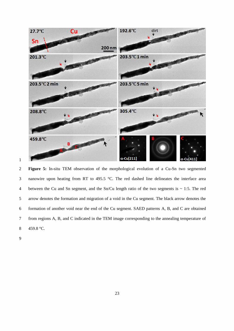
Fig. 5 illustrates the in-situ TEM observation of the morphological evolution of another Cu-21
Sn two segmented nanowire while it is being heated from RT to 459.8 °C. The dashed line indicates 22
the interface area of the two segments. The Sn/Cu length ratio of the two segments is about 1:5, i.e., 23
the Sn segment is much shorter compared to the Cu segment. Different from the soldering reaction 24
shown in Fig. 2, one can see that there is no any bulge formation on the nanowire annealed up to ~ 25
460 °C, suggesting that no IMC formation occurs throughout the annealing process. This is further 26

9
confirmed by electron diffraction analysis of the reacted nanowire. The SAED patterns of A, B, C, are 1
obtained from the representative areas of A, B, C, respectively, as marked in the TEM image of the 2
sample heated at 459.8 °C. The electron diffraction analyses reveal that areas A and C are α- Cu(Sn), 3
which is a solid solution of Sn in Cu, and area B corresponds to the amorphous Sn oxide layer. While 4
there is no IMC formation, Kirkendall voids still develop in the nanowire. As seen from the TEM 5
image obtained at 192.6 °C, a small void (indicated by the red arrow on the TEM image) forms in the 6
Cu segment, where a small dirt (which is the organic remanent from the sample preparation and has 7
no effect on the soldering reaction or void formation) slightly on the right of the void serves as a 8
marker revealing the migration of the void during the annealing process. One can see that the void 9
first grows larger, then shrinks, and disappears at 203.5 °C, and reappears at another location of the 10
nanowire (see the TEM image of the sample at 203.5 °C (and holding for 5 min), where a small void 11
forms on the right side of the small dirt). The void grows larger with increasing annealing temperature, 12
and meanwhile, another void forms on the right end of the Cu segment (see the TEM image obtained 13
at 305.4 °C). 14
The formation of Kirkendall voids in the Cu segment demonstrates that the diffusion of Cu in 15
Sn is faster than that of Sn in Cu. This is similar as the diffusion of Cu and Sn in the IMC, in which 16
Cu diffuses faster than Sn, as revealed from the in-situ TEM observation shown in Fig. 2. Fig. 5 also 17
reveals that the IMC formation requires the availability of sufficient amount of Sn, which depends on 18
the relative lengths of the Cu and Sn segments. For the case shown in Fig. 5, the Sn segment is too 19
short compared to the Cu segment, for which the fast composition homogenization of the nanowire by 20
interdiffusion of Cu and Sn results in the formation of the solid solution of Sn in Cu. 21
Fig. 6 illustrates the metallurgical soldering reaction of a Cu-Sn nanowire with roughly equal 22
length (Cu/Sn length ratio = 1:1) of the Cu and Sn segments. Fig. 6(a) is an STEM DF image of the 23
nanowire before it is heated, where the Sn segment appears brighter than the Cu segment because Sn 24
atom is heavier than Cu. Fig. 6(b) is an in-situ STEM DF image of the nanowire heated at 491 °C, 25
which shows that the nanowire has relatively uniform contrast, suggesting that the interdiffusion of 26
10
Cu and Sn occurs along the nanowire. Fig. 6(b) also reveals the formation of several bulges on the Cu 1
segment (this is similar as the nanowire shown in Fig. 2, where the IMC bulge forms also on the Cu 2
segment). Fig. 6(c) is an in-situ STEM BF image of the nanowire that is being heated at 491 °C, 3
which shows that there is a Kirkendall void on the right near the end of the Cu segment. Fig. 6(d) 4
shows SAED patterns obtained from the representative areas of the nanowire marked in Fig. 6(c). 5
Diffraction pattern A obtained from the area on the left end of the Sn segment shows a limited number 6
of diffusing rings, which are typical features of an amorphous structure, demonstrating that the left 7
end of the Sn segment is not reacted and still in its melt state at the high temperature. SAED patterns 8
B, C, and E can be indexed well with γ-Cu3Sn while diffraction pattern D obtained from area D 9
matches well with ε-Cu3Sn. The electron diffraction analysis reveals that a compound consisting of 10
various IMC phases has been developed in the Cu segment, in which the ε-Cu3Sn phase transforms 11
into the high-temperature phase of γ-Cu3Sn as the nanowire is heated up to 491 °C. The kirkendall 12
void near the right side of the nanowire must be formed after the ε-Cu3Sn→ γ-Cu3Sn phase 13
transformation initiates (at relatively high temperature) otherwise it will shut off the diffusion path 14
before γ-Cu3Sn is formed. The in-situ TEM observation also demonstrates clearly the complete 15
reaction of the Cu segment owing to the availability of the sufficient Sn (there is still remaining Sn in 16
its melt state). 17
To further demonstrate the effect of the relative lengths of the Cu and Sn segments on the 18
IMC formation, Fig. 7 shows the in-situ TEM observation of the soldering reaction of a Cu-Sn 19
nanowire for which the Sn segment is much longer than the Cu segment (the Sn/Cu length ratio is 20
about 7:5). One can see that a Kirkendall void (marked by the red arrow in the TEM images) starts to 21
form in the Cu segment at ~ 186.6 °C (where a remanent organic dirt on the left of the void can serve 22
as a marker to reveal the void growth and migration in the course of the metallurgical reaction). With 23
slightly increasing the annealing temperature, the void grows larger first, then shrinks and disappears 24
at ~ 203.7 °C, and then re-appears on the left of the dirt at 204 oC. Meanwhile, a bulge becomes 25
clearly visible in the Cu segment adjacent to the void at ~ 204.3 °C and grows larger with the 26

11
temperature increase to 226.8 °C. At 227.6 °C (and holding for 10 min at this temperature), one can 1
see that the bulge shrinks. This trend continues with further increasing the soldering temperature and 2
the bulge’s volume becomes almost disappeared at 497.1 °C. The in-situ TEM images also reveal that 3
there is no obvious change in the size of the void after the complete breakage of the nanowire at 4
204.4 °C. 5
Fig. 8 gives the EDS elemental mapping characterization of the reacted nanowire shown in 6
Fig. 7. Fig. 8(b) shows the Cu and Sn maps of the area indicated by the dashed rectangle on the left 7
shown in Fig. 8(a). The Cu mapping shows that areas A, C, E have much stronger Cu intensity than 8
areas B and D while the Sn mapping reveals that area A has much weaker Sn signal than areas B, C, 9
D, and E. Fig. 8(c) corresponds to the Cu and Sn mapping of the area indicated by the dashed 10
rectangle on the right shown in Fig. 8(a), from which one can see that the intensities for Cu and Sn are 11
relatively uniform, suggesting the homogenization of the composition on this end. 12
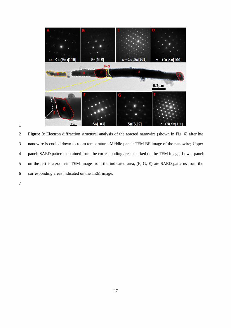
The composition mappings are correlated with structural analysis by electron diffraction as 13
shown in Fig. 9. Diffraction pattern A is obtained from area A of the nanowire as seen in the TEM 14
image in the middle panel, which reveals that area A is a solid solution of Sn in Cu. This is also 15
consistent with the Cu and Sn mapping shown in Fig. 8(b). The formation of the Cu(Sn) solid solution 16
suggests that the Cu segment is not completely consumed. This is because of the formation of the 17
Kirkendall void between areas A and B, which breaks up the nanowire and thus blocks interdiffusion 18
of Cu and Sn. Diffraction B is acquired from area B as indicated in the corresponding TEM image on 19
the middle panel in Fig. 9, which reveals that this area is pure Sn, consistent with the Cu and Sn maps 20
shown in Fig. 8(b). The electron diffraction patterns obtained from areas C, D and E show that areas C 21
and E are ε-Cu3Sn while area D is γ-Cu3Sn. The various IMC phases is due to the temperature effect, 22
for which the η-Cu6Sn5 forms first then transforms into and then to the high-temperature phase of γ-23
Cu3Sn by following the transformation path, η-Cu6Sn5 → ε-Cu3Sn → γ-Cu3Sn, with increasing the 24
soldering temperature. According to the Cu-Sn phase diagram the η-Cu6Sn5 is not stable and will 25
transform into ε-Cu3Sn above 415℃. The absence of η-Cu6Sn5 in the reacted nanowire shown in Fig. 26
12
9 suggests that the η-Cu6Sn5 phase is completelytransformed to ε-Cu3Sn. Areas C and E are the 1
remaining ε-Cu3Sn phase. This is also consistent with the result shown in Fig. 6, which shows the co-2
existence of the γ-Cu3Sn and ε-Cu3Sn phases due to the incomplete conversion of the η-Cu6Sn5phase. 3
Diffraction patterns F and G are obtained from areas F and G composing of two grains as seen from 4
the zoom-in TEM image shown on the bottom panel in Fig. 9, which indicate these areas are un-5
reacted Sn formed in between the IMC grains. 6
Our in-situ TEM observations described above reveal that the phase and morphological 7
evolution of the Cu-Sn metallurgical reaction depend on the relative lengths of the Sn and Cu 8
segments. A few representative length ratios of the Sn and Cu segments were examined in our in-situ 9
TEM experiments including the Sn/Cu length ratio of ~ 1 : 5 (see Fig. 5), ~ 1 : 3 (Fig. 2), ~ 1 : 1(Fig. 10
6), and ~ 7:5 (Fig. 7). Several trends can be drawn from the set of the samples. First, one can see that 11
decreasing the relative length of the Sn segment leads to void formation at the end of the Sn segment 12
due to the complete depletion of the Sn segment for IMC formation (Fig. 2). If the length of the Sn 13
segment is too short, Sn forms a solid solution in Cu without IMC formation (Fig. 5). However, 14
despite the relative lengths of the two segments, Kirkendall void formation in the Cu segment always 15
occurs due to the faster diffusion of Cu in Sn as well as in IMC than that of Sn in Cu and IMC. These 16
voids can migrate in the Cu segment and the void growth sometimes can cause breakage of the Cu 17
segment, which shut off the paths for the interdiffusion of Cu and Sn. Second, the bulge (η-Cu6Sn5) 18
formation occurs first in the Cu segment around 200 °C, suggesting that its formation is related to the 19
inter-diffusion of Sn into Cu rather than the Cu diffusion into Sn despite for the faster diffusion of Cu 20
into Sn. Third, increasing the length of the Sn segment results in un-reacted Sn, which exists not only 21
in the original Sn segment and but also in between IMC grains formed by interdiffusion of Cu and Sn. 22
Fourth, increasing the annealing temperature up to ~ 500 °C results in two phase transformation paths, 23
depending on the availability of Cu, i.e., η-Cu6Sn5 → ε-Cu3Sn → δ-Cu41Sn11 for a long Cu segment 24
(i.e., Figs. 2 and 3), or η-Cu6Sn5 → ε-Cu3Sn → γ-Cu3Sn for a shorter Cu segment (Figs. 6, 7, and 9). 25
Fig. 10 show schematically the soldering reactions for the two-segment Cu-Sn nanowires with 26

13
the different length ratios of the two segments. Fig. 10(a) corresponds to the reaction with a very short 1
Sn segment, which results in the formation of a solid solution of Sn in Cu and Kirkendall voids due to 2
the faster diffusion of Cu than Sn. Fig. 10(b) corresponds to the Cu-Sn reaction with increased length 3
of the Sn segment, for which the Sn segment is completely consumed for IMC formation by reacting 4
with incoming Cu. As a result, a void is formed at the end of the Sn segment. Meanwhile, a 5
Kirkendall void is developed in the Cu segment owing to the faster diffusion of Cu in the IMC than 6
that of Sn. Fig. 10(c) illustrates the Cu-Sn reaction with similar lengths of the Cu and Sn segments, for 7
which Cu is completely consumed to form IMCs with the concomitant formation of a Kirkendall void 8
in the Cu segment near the end. Fig. 10(d) corresponds to the Cu-Sn reaction, where the Sn segment is 9
longer than the Cu segment, for which both Sn and Cu are not completely consumed. The incomplete 10
reaction of the Cu segment at the right end is due to the formation of a Kirkendall void that shuts off 11
the diffusion paths of Cu and Sn while the existence of un-reacted Sn is due to the insufficient Cu 12
available to react with Sn. 13
The void formation proposes a big reliability threat to the mechanical strength of the joints, 14
thus the kirkendall void formed between the Cu segment and the Sn solder joining segment is 15
undesirable. Because the void formation is mainly due to the faster diffusion of Cu than that of Sn in 16
ε-Cu3Sn/η-Cu6Sn5 IMCs as well as in Sn at relative low temperature (~200°C), increasing 17
temperature ramp rate and reducing the soak time of soldering reflow, or adding a barrier layer 18
between the base metal segment and the solder segment to inhibit the diffusion of Cu into Sn may be a 19
good approach to mitigate voiding and improve the integrity of the interconnection. During the 20
soldering process, the intermetallic compounds (IMC) formed between the solder and the base metal 21
signify the proper bonding between solder and substrate. But excess growth of the IMC layer may 22
result in degradation of the joint/interconnection. For the nanowire with a very short Sn segment, such 23
as the Sn/Cu length ratio of ~ 1:5 shown in Fig. 5, there is no IMC formed, which is undesired for 24
soldering. The nanowire with an equal or longer Sn segment results in a thicker IMC layer as 25
compared to the one with longer Cu segment. η-Cu6Sn5 is the initially formed phase between Cu and 26

14
Sn segments and it may remain as the η-Cu6Sn5 phase or reacts with incoming Cu to transform into ε-1
Cu3Sn, depending on the availability of Cu. The growth of ε-Cu3Sn requires the supply of Cu atoms 2
and consumption of Cu6Sn5 at the Cu/Cu6Sn5 interface. As for the nanowire with a longer Sn segment, 3
all the Cu atoms react with Sn, resulting Cu6Sn5 and un-reacted Sn. However, the nanowire with a 4
longer Cu segment has remanent Cu atoms when all the Sn is transformed into Cu6Sn5, thus leading to 5
the formation of ε-Cu3Sn at the comsumption of both remaining Cu and Cu6Sn5. Given sufficient 6
amount of Cu, the η-Cu6Sn5 would be completely converted to ε-Cu3Sn phase. Thus, a longer Cu 7
segment favors its transformation to the ε-Cu3Sn phase. During thermal cycling or reflow process 8
around 250 °C, the allotropic transformation of the η-Cu6Sn5 hexagonal structure to the monoclinic 9
structure around 186~189°C accompanies 2.15% volume expansion[52]
, which is unfavorable for the 10
mechanical integrity of the solder joints/interconnection. Therefore the nanowire with a relatively 11
longer Cu segment is desired for soldering because of its formation of the ε-Cu3Sn phase at the 12
soldering reaction temperature. 13
14
4. Conclusions 15
In-situ TEM has been employed to visualize the Cu-Sn soldering reaction of two-segmented 16
Cu-Sn nanowires. We show that both the formation of the Cu-Sn intermetallic compounds (IMC) and 17
their phase evolution depend on the relative lengths of the Cu and Sn segments. A short Sn segment 18
results in the formation of a solid solution of Sn in Cu. Increasing the relative length of the Sn 19
segment leads to the formation of IMCs and Kirkendall voids in the Cu segment. Upon increasing the 20
soldering temperature up to ~ 500 °C, two phase transformation pathways occur, η-Cu6Sn5 → ε-Cu3Sn 21
→ δ-Cu41Sn11 for a long Cu segment and η-Cu6Sn5 → ε-Cu3Sn → γ-Cu3Sn for a short Cu segment. 22
The formation of Kirkendall voids in the Cu segments can lead to the breakage of the Cu segment, 23
which shuts off the inter-diffusion of Cu and Sn and thus lead to the changes in the phase 24
transformation pathways of the IMCs. These results demonstrate that Cu diffuses faster than Sn in the 25
Cu-Sn IMCs, which is the underlying cause of the dependence of the reaction products on the relative 26

15
lengths of the Cu and Sn segments. 1
2
Acknowledgement: 3
This work was supported by the National Science Foundation under NSF Collaborative Research 4
Award Grant CMMI-1233806. Research carried out in part at the Center for Functional 5
Nanomaterials, Brookhaven National Laboratory, which is supported by the U.S. Department of 6
Energy, Office of Basic Energy Sciences, under Contract No. DE-AC02-98CH10886. 7
8
References: 9
[1] Y. Lin, W. Jian, Nano Letters 2008, 8, 3146. 10
[2] Y. Peng, T. Cullis, B. Inkson, Nano Letters 2008, 9, 91. 11
[3] H. R. Kotadia, P. D. Howes, S. H. Mannan, Microelectronics Reliability 2014. 12
[4] H. Lai, J. Duh, Journal of Electronic Materials 2003, 32, 215. 13
[5] J. H. Pang, B. Xiong, C. Neo, X. Mang, T. Low, "Bulk solder and solder joint properties for 14
lead free 95.5 Sn-3.8 Ag-0.7 Cu solder alloy", presented at Electronic Components and 15
Technology Conference, 2003. Proceedings. 53rd, 2003. 16
[6] J. Li, P. A. Agyakwa, C. M. Johnson, D. Zhang, T. Hussain, D. G. McCartney, Surface and 17
Coatings Technology 2010, 204, 1395. 18
[7] L. M. Lee, H. Haliman, A. A. Mohamad, Soldering & Surface Mount Technology 2013, 25, 19
15. 20
[8] H. Jiang, K. Moon, C. Wong, Microelectronics Reliability 2013, 53, 1968. 21
[9] H. Jiang, K. Moon, C. Wong, "Tin/silver/copper alloy nanoparticle pastes for low temperature 22
lead-free interconnect applications", presented at Electronic Components and Technology 23
Conference, 2008. ECTC 2008. 58th, 2008. 24
[10] F. Gao, S. Mukherjee, Q. Cui, Z. Gu, The Journal of Physical Chemistry C 2009, 113, 9546. 25
[11] Q. Cui, F. Gao, S. Mukherjee, Z. Gu, Small 2009, 5, 1246. 26
[12] J. Wang, M. Tian, T. E. Mallouk, M. H. Chan, Nano Letters 2004, 4, 1313. 27
[13] C. K. Jin, N. B. P. Christine, C. M. Ting, D. S. Tong, "Challenges of Pd-coated Cu wire 28
bonding on C65 Al bond pad low-k wafer with BOA structure", presented at Electronics 29
Packaging Technology Conference (EPTC), 2011 IEEE 13th, 2011. 30

16
[14] M. Alam, Y. Chan, K. Tu, Journal of Applied Physics 2003, 94, 4108. 1
[15] Y. Chan, A. C. So, J. Lai, Materials Science and Engineering: B 1998, 55, 5. 2
[16] J. Yoon, C. Lee, S. Jung, Journal of Electronic Materials 2003, 32, 1195. 3
[17] A. Sharif, M. Islam, Y. Chan, Materials Science and Engineering: B 2004, 113, 184. 4
[18] Y. Jee, Y. Ko, J. Yu, Journal of Materials Research 2007, 22, 1879. 5
[19] C. Yu, W. Chen, J. Duh, Intermetallics 2012, 26, 11. 6
[20] F. Che, J. H. Pang, Journal of Alloys and Compounds 2012, 541, 6. 7
[21] M. Islam, A. Sharif, Y. Chan, Journal of Electronic Materials 2005, 34, 143. 8
[22] T. Huang, H. Tseng, Y. Hsiao, C. Cheng, C. Lu, C. Liu, Electrochemical and Solid-State 9
Letters 2011, 14, H393. 10
[23] Q. Li, Y. Chan, Journal of Alloys and Compounds 2013, 567, 47. 11
[24] W. Peng, E. Monlevade, M. E. Marques, Microelectronics Reliability 2007, 47, 2161. 12
[25] T. Laurila, T. Mattila, V. Vuorinen, J. Karppinen, J. Li, M. Sippola, J. K. Kivilahti, 13
Microelectronics Reliability 2007, 47, 1135. 14
[26] T. Liu, C. Liu, Y. Huang, C. Chen, K. Tu, Scripta Materialia 2013, 68, 241. 15
[27] R. Labie, W. Ruythooren, J. Van Humbeeck, Intermetallics 2007, 15, 396. 16
[28] F. Gao, Z. Liu, G. Zhou, J. C. Yang, Z. Gu, Science of Advanced Materials 2012, 4, 881. 17
[29] Q. Cui, K. Rajathurai, W. Jia, X. Li, F. Gao, Y. Lei, Z. Gu, The Journal of Physical 18
Chemistry C 2010, 114, 21938. 19
[30] H. Hsiao, C. Liu, H. Lin, T. Liu, C. Lu, Y. Huang, C. Chen, K. Tu, Science 2012, 336, 1007. 20
[31] J. Suh, K. Tu, N. Tamura, Journal of Applied Physics 2007, 102, 063511. 21
[32] J. Li, P. Agyakwa, C. Johnson, Acta Materialia 2011, 59, 1198. 22
[33] D. Ma, W. Wang, S. Lahiri, Journal of Applied Physics 2002, 91, 3312. 23
[34] J. Gorlich, G. Schmitz, K. N. Tu, Applied Physics Letters 2005, 86, 053106. 24
[35] X. Ma, F. Wang, Y. Qian, F. Yoshida, Materials Letters 2003, 57, 3361. 25
[36] J. Yoon, B. Noh, B. Kim, C. Shur, S. Jung, Journal of Alloys and Compounds 2009, 486, 142. 26
[37] B. Chao, S. Chae, X. Zhang, K. Lu, J. Im, P. Ho, Acta Materialia 2007, 55, 2805. 27
[38] A. Munding, H. Hübner, A. Kaiser, S. Penka, P. Benkart, E. Kohn, in Wafer Level 3-D ICs 28
Process Technology, Springer, 2008, 1. 29
17
[39] K. Tu, Acta Metallurgica 1973, 21, 347. 1
[40] T. Laurila, V. Vuorinen, J. Kivilahti, Materials Science and Engineering: R: Reports 2005, 49, 2
1. 3
[41] H. Kim, K. Tu, Physical Review B 1996, 53, 16027. 4
[42] J. Görlich, G. Schmitz, K. Tu, Applied Physics Letters 2005, 86, 053106. 5
[43] L. M. Lee, A. A. Mohamad, Advances in Materials Science and Engineering 2013, 2013. 6
[44] S. Kumar, C. A. Handwerker, M. A. Dayananda, Journal of Phase Equilibria and Diffusion 7
2011, 32, 309. 8
[45] B. Kim, G. Lim, J. Kim, K. Lee, Y. Park, Y. Joo, "Intermetallic compound and Kirkendall 9
void growth in Cu pillar bump during annealing and current stressing", presented at 10
Electronic Components and Technology Conference, 2008. ECTC 2008. 58th, 2008. 11
[46] G. Allen, R. Bayles, W. Gile, W. Jesser, Thin solid films 1986, 144, 297. 12
[47] S. Lai, J. Guo, V. Petrova, G. Ramanath, L. Allen, Physical Review Letters 1996, 77, 99. 13
[48] H. Jiang, K. Moon, H. Dong, F. Hua, C. Wong, Chemical Physics Letters 2006, 429, 492. 14
[49] P. Villars, L. D. Calvert, Pearson's handbook of crystallographic data for intermetallic 15
phases, Vol. 2, American Society for Metals Metals Park, OH, 1985. 16
[50] N. Saunders, A. Miodownik, Bulletin of Alloy Phase Diagrams 1990, 11, 278. 17
[51] D. Li, P. Franke, S. Fürtauer, D. Cupid, H. Flandorfer, Intermetallics 2013, 34, 148. 18
[52] K. Nogita, C. Gourlay, S. McDonald, Y. Wu, J. Read, Q. Gu, Scripta Materialia 2011, 65, 19
922. 20
21
22
23
24

18
Figure captions: 1
2
Figure 1: As-prepared Cu-Sn two segmented nanowires by a template assisted electrodeposition 3
method. (a) a representative SEM image of Cu-Sn two segment nanowires; (b) a STEM bright-field 4
image of a Cu-Sn nanowire; (c, d) STEM EDS elemental mapping of the Cu-Sn nanowire shown in (b) 5
with the Sn map in red and Cu map in blue; (e, f) Selected-area electron diffraction patterns obtained 6
from the Sn and Cu segments of the nanowire shown in (b). 7
19
1
Figure 2: In-situ TEM observation of the morphological evolution of a Cu-Sn two segmented 2
nanowire upon heating from room temperaeture (RT) to 495.5 °C. The red dashed line delineate the 3
interface area between the Cu and Sn segment, and the Sn/Cu length ratio of the two segments is ~ 1:3. 4
The red arrow on the TEM image corresponding to the annealing temperature of 200 °C denotes the 5
formation of a bulge in the Cu segment near the Sn/Cu interface. The void formation in the Sn and Cu 6
segments is denoted by black arrows at the corresponding annealing temperatures. 7

20
1
21
1
Figure 3: Elemental mapping and structural analysis of the reacted Cu-Sn nanowire shown in Fig. 2. 2
(a) BF-TEM image of the Cu-Sn nanowire after being annealed at 495.5 °C; (b, c) STEM EDS 3
elemental mapping of the annealed nanowire with the Cu map in green and Sn map in red; 4
(d, e) SAED patterns obtained from areas "1" and "2" indicated in (a), respectively; (f, g) 5
atomicstructures of ε-Cu3Sn and δ-Cu41Sn11 used for simulating the electron diffraction patterns 6
shown in (h and i); (j, k, l) SAED patterns obtained from areas "3", "4", and "5" indicated in (a). 7

22
1
Figure 4: Formation of η-Cu6Sn5 from the isothermal annealing of a Cu-Sn nanowire at ~ 210 °C. (a) 2
TEM image of an unreacted Cu-Sn two-segment nanowire at room temperature, where the dashed line 3
denotes the location of the interface between the Sn and Cu segments, insets are SAED patterns from 4
the Cu and Sn segments; (b) TEM image of the nanowire reacted at ~ 210 °C for 20 min, where the η-5
Cu6Sn5 phase is formed in the original Cu segment, insets are SAED patterns obtained from the 6
indicated regions. 7
8
23
1
Figure 5: In-situ TEM observation of the morphological evolution of a Cu-Sn two segmented 2
nanowire upon heating from RT to 495.5 °C. The red dashed line delineates the interface area 3
between the Cu and Sn segment, and the Sn/Cu length ratio of the two segments is ~ 1:5. The red 4
arrow denotes the formation and migration of a void in the Cu segment. The black arrow denotes the 5
formation of another void near the end of the Cu segment. SAED patterns A, B, and C are obtained 6
from regions A, B, and C indicated in the TEM image corresponding to the annealing temperature of 7
459.8 °C. 8
9

24
1
Figure 6: Soldering reaction of a Cu-Sn nanowire with roughly equal lengths of the Cu and Sn 2
segments (Cu/Sn length ratio ~ 1:1). (a) a STEM DFimage of the nanowire before annealing; (b) a 3
STEM DF of the Cu-Sn nanowire while it is being annealed at 491 °C; (c) a TEM bright-field image 4
of the Cu-Sn nanowire while it is being annealed at 491 °C; (d) SAED patterns obtained from the 5
corresponding areas indicated in (c) while the nanowire is being annealed at 491 °C. 6
7

25
1
Figure 7: In-situ TEM observation of the morphological evolution of a Cu-Sn two segmented 2
nanowire upon heating from RT to 497.1 °C. The red dashed line delineate the interface area between 3
the Cu and Sn segment, and the Sn/Cu length ratio of the two segments is ~ 5:2. The red arrows 4
denote the formation and migration of a Kirkendall void in the Cu segment, and the black arrows 5
denote the formation, growth, and shrinkage of a bulge near the void. 6
7

26
1
Figure 8: Elemental mapping of the reacted Cu-Sn nanowire shown in Fig. 6. (a) a STEM BF image 2
of the Cu-Sn nanowire after being annealed at 497.1 °C; (b) STEM EDS elemental mapping of the 3
area indicated by the red dashed rectangle on the left shown in (a) with the Cu map in blue and Sn 4
map in red; (c) STEM EDS elemental mapping of the area indicated by the red dashed rectangle on 5
the right in (a). 6
7
27
1
Figure 9: Electron diffraction structural analysis of the reacted nanowire (shown in Fig. 6) after hte 2
nanowire is cooled down to room temperature. Middle panel: TEM BF image of the nanowire; Upper 3
panel: SAED patterns obtained from the corresponding areas marked on the TEM image; Lower panel: 4
on the left is a zoom-in TEM image from the indicated area, (F, G, E) are SAED patterns from the 5
corresponding areas indicated on the TEM image. 6
7

28
1
Figure 10: Schematic showing the Cu-Sn soldering reaction of the segmented Cu-Sn nanowires with 2
the different relative lengths of the Cu and Sn segments (the grey line represents a native oxide layer 3
formed from the sample preparation). (a) the reaction of a long Cu segment with a small Sn segment 4
results in the formation of a solid solution of Sn in Cu and Kirkendall voids (no IMC formation); (b) 5
the reaction of a long Cu segment with a Sn segment with the relatively increased length results in 6
IMC formation that consumes all the Sn segment, thereby forming a void at the end of the Sn segment; 7
(c) reaction of the Cu-Sn nanowire with roughly equal lengths of the Cu and Sn segments that results 8
in the completely consumed Cu segment; (d) reaction of the Cu-Sn nanowire with a much longer Sn 9
segment that results in both incomplete Cu and Sn segments. 10
11
12