In Situ SEM Solidification Study of Ga and eGaIn
28
In Situ SEM Solidification Study of Ga and eGaIn A Characterization Technique for Monitoring the Microstructural Evolution of Liquid Metals A Senior Project Presented to the Faculty of the Materials Engineering Department at Cal Polytechnic State University, San Luis Obispo In Partial Fulfillment of the Requirements for a Bachelor of Science Degree in Materials Engineering By Jeremy Del Aguila in collaboration with Dr. Linda Vanasupa June 15, 2018 ©Jeremy Del Aguila
Transcript of In Situ SEM Solidification Study of Ga and eGaIn

In Situ SEM Solidification Study of Ga and eGaIn A Characterization Technique for Monitoring the Microstructural Evolution of Liquid Metals
A Senior Project Presented to the Faculty of the Materials Engineering Department at Cal Polytechnic State University, San Luis Obispo In Partial Fulfillment of the Requirements for a Bachelor of Science Degree in Materials Engineering
By Jeremy Del Aguila in collaboration with Dr. Linda Vanasupa
June 15, 2018
©Jeremy Del Aguila

In Situ SEM Solidification Study of Ga and eGaIn Del Aguila, J.
1 | P a g e Department of Materials Engineering, Cal Poly San Luis Obispo
Approval Page
Project Title: In Situ SEM Solidification Study of Ga and eGaIn : A Characterization Technique
for Monitoring the Microstructural Evolution of Liquid Metals
Author: Jeremy del Aguila
Date Submitted: June 13, 2018
Prof. Linda Vanasupa ______________________________
Faculty Advisor Signature
Prof. Trevor Harding ______________________________
Department Chair Signature
CAL POLY STATE UNIVERSITY
Materials Engineering Department
Since this project is a result of a class assignment, it has been graded and
accepted as fulfillment of the course requirements. Acceptance does not imply
technical accuracy or reliability. Any use of information in this report is done
at the risk of the user. These risks may include catastrophic failure of the
device or infringement of patent or copyright laws. The students, faculty, and
staff of Cal Poly State University, San Luis Obispo cannot be held liable for
any misuse of the project.

In Situ SEM Solidification Study of Ga and eGaIn Del Aguila, J.
2 | P a g e Department of Materials Engineering, Cal Poly San Luis Obispo
Table of Contents
Acknowledgements 3
List of Figures 4
List of Tables 5
Abstract 6
Introduction 7
Methods and Methodology 12
Results and Discussion 16
Conclusions and Recommendations 21
References 22
Appendix A: Literature Review 24
Appendix B: Heat Transfer Model Computations 27

In Situ SEM Solidification Study of Ga and eGaIn Del Aguila, J.
3 | P a g e Department of Materials Engineering, Cal Poly San Luis Obispo
Acknowledgements
I’d like to thank everyone involved in making this project possible. Dr. Linda Vanasupa for
being my senior project advisor and taking on the responsibility of being my thought partner and
mentor throughout the process. Victor Granados, for teaching me how to use the SEM and
helping me conduct the preliminary experimental studies. Dr. Yong Hao and Glenn Lee for being
generous and purchasing the gallium metal. Lastly, the Materials Engineering Department for
allowing me to perform an independent project and providing the equipment, faculty, and
resources to do so.

In Situ SEM Solidification Study of Ga and eGaIn Del Aguila, J.
4 | P a g e Department of Materials Engineering, Cal Poly San Luis Obispo
List of Figures
Figure 1: Phase diagrams of the (a) pure Ga and (b) binary eutectic eGaIn systems.
Figure 2: Equilibrium cooling path for (a) eGaIn (b) Ga and (c) evolution of eutectic
microstructure upon equilibrium cooling.
Figure 3: Schematic diagram of sample preparation (a) Bulk sample heated in hot bath (b)
spheres drop cast onto weigh boats (c) preheated and etched spheres
Figure 4: Before and after image of etching Ga with 60 µL of 3 % HCl (a) Ga/Ga2O3 (b) etched
Ga with mirror finish.
Figure 5: Instrument and equipment used for the solidification studies of Ga and eGaIn (a)
Peltier cooling stage with stainless-steel specimen holder (b) thermoelectric stage controller and
(c) FEI Quanta 200 SEM equipped with stage.
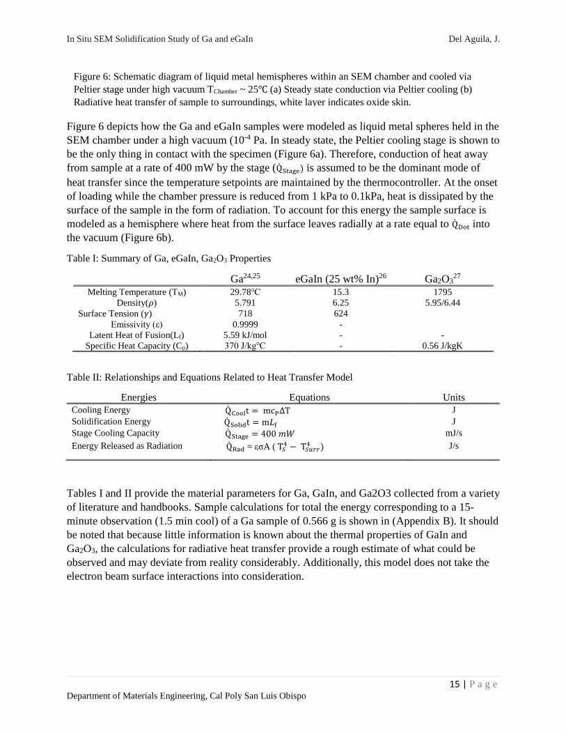
Figure 6: Schematic diagram of liquid metal hemispheres within an SEM chamber and cooled
via Peltier stage under high vacuum TChamber ~ 25℃ (a) Steady state conduction via Peltier
cooling (b) Radiative heat transfer of sample to surroundings, white layer indicates oxide skin.
Figure 7: Backscattered SEM micrographs of 0.2599 g sample of Ga heated to 55℃, etched, and
air cooled as seen at (a) 498 X (b) 2818 X.
Figure 8: The prevalence of gaseous bubble formation on a Ga surface (a) seen at 30 X (b)
bubbles along the vertical surface are maintained by the high surface tension.
Figure 9: Backscattered (a) and Secondary Electron (b) micrographs of Ga sample. Images show
how information of the image differs due to different electronic signals and contrast mechanisms
captured by the two detectors. The BSD images shows a difference in phases between the
material within the cavity where the SE image shows a topographical representation of it.
Figure 10: Backscattered SEM micrographs Ga heated to 55℃, etched, and off gassed for 1 min
(a) 4098 X (b) 5802 X. The microstructure is porous and depicts the effect of gas diffusion into
the surface from the etching process. Microstructure appears glasslike9.
Figure 11: Backscattered SEM micrographs of liquid filled defects on Ga surface after sample is
superheated and cooled (a) Image of specimen surface at the onset of imaging (b) solidified
microstructure after being cooled to 10℃ and maintained for >10 min.
Figure12: Backscattered (a) and Secondary Electron (b) SEM micrographs of GaIn sample
heated to 50℃, etched while hot, and off gassed for 1 min. Images show solidified
microstructural features such as dendrites and eutectic lamellae just under the surface within
cavities.
Figure 13: Images taken from a video recording of GaIn sample etched at RT, and off gassed for
1 min. showing how a cavity acts as a viewing window for mushy zone and underlying liquid
phase. (a) void (b) coalescence of void showing underlying Ga rich liquid phase (c) solidified
region after 15 min.

In Situ SEM Solidification Study of Ga and eGaIn Del Aguila, J.
5 | P a g e Department of Materials Engineering, Cal Poly San Luis Obispo
List of Tables
Table I: Summary of Ga, eGaIn, Ga2O3 Properties
Table II: Relationships and Equations Related to Model

In Situ SEM Solidification Study of Ga and eGaIn Del Aguila, J.
6 | P a g e Department of Materials Engineering, Cal Poly San Luis Obispo
Abstract
Scanning electron microscopy (SEM) video recording is used to characterize the solidification of
small volumes of 99.999% pure gallium (Ga) and eutectic gallium-indium (eGaIn) under a high
vacuum environment. Specimen are superheated to 55℃ using a hot plate, cast into spherical
droplets, and cooled in situ by means of a Peltier cooling stage. Special attention is paid to the
preparation of the specimen prior to viewing because of gallium and its alloys’ nature to form an
oxide layer when melted and air cooled. Solidification of unetched Ga is impaired due to the
oxide layer that solidifies first, inhibiting the observation of microstructural features. Heated
samples are etched using a 3% HCl solution to yield an oxide-free mirror finish prior to imaging.
A series of observations are performed to determine whether the use of the etchant is effective in
removing the oxide layer to enhance viewing capabilities of the solidification process. Video
recordings and images show that the application of etchant changes the surface chemistry such
that the oxide layer is reduced to a metallic chloride and cause droplets to bead up into spheres
showing a decrease in surface tension. Additionally, cavities are observed at the surface of GaIn
caused by bubbles formation during the etching step that act as viewing windows for
microstructural evolution during solidification. The technique developed and employed in the
preset study can be replicated and performed for other liquid metals however should be made
more robust for future application.
Keywords: Materials Characterization, liquid metals, Gallium, Gallium Indium, eutectic alloy,
solidification, scanning electron microscopy, SEM, in situ SEM, hydrochloric acid etch, HCl,
high vacuum mode

In Situ SEM Solidification Study of Ga and eGaIn Del Aguila, J.
7 | P a g e Department of Materials Engineering, Cal Poly San Luis Obispo
I. Introduction
Problem Statement
The FEI Quanta 200 scanning electron microscope (SEM) used in the Materials Engineering
Department comes standard with a Peltier cooling stage for ESEM mode operation. The
capabilities of the stage have not recently been explored in the department and holds potential as
a method for studying the solidification of liquid metals in situ.
Project Objective
This study aims to develop a replicable technique using HVSEM and the Peltier cooling stage to
study the microstructural evolution of liquid metals during solidification.
A Brief History of SEM Technology
Since the development of the first scanning electron microscope (SEM) in 1938 by
Zworykin1, SEM technology has become an invaluable tool for imaging the microstructural
characteristics of solid objects. The morphology and composition of a material can be examined
and analyzed from high resolution images rendered from the signals that are generated as a
focused electron beam interacts with a localized region on a sample surface. The resulting
micrographs provide qualitative information about a material’s crystallographic, and
microstructural characteristics that can be correlated to magnetic, electrical, and mechanical
properties2.
The largest limitation of early SEM technology was that it required a good vacuum for the
generation and propagation of an electron beam. This presented a design constraint on
observational experimentation because it restricted how specimen should be prepared and
imaged. Typically, for conventional SEM analysis, a specimen must be preserved, dehydrated,
and coated with a metal to conduct excess electrons to ground3. Additionally, a high vacuum
environment does not allow for wet or biological specimen to be observed in their natural state
because of the possibility of contaminating the chamber with debris or gassing. Modern SEM
instrumentation however is no longer subject to the same limitations since the advent of variable
pressure SEMs in the 1980’s4. Current SEMs such as the FEI Quanta 200 provide a variety of
viewing modes that vary by pressure and ambient environment. The available modes are low
vacuum (LV), high vacuum (HV), and environmental (E).
To lay the foundation for the development of the characterization technique reported herein, a
discussion about recent in situ methods that employ the different modes in SEM technology is
discussed. For a more in depth look at how images are formed in an SEM, specimen interactions,
and signal detection refer to the literature review5 in (Appendix A).
In Situ Methods
In recent years material scientists and engineers have realized environmental scanning electron
microscopy (ESEM) as a method of performing in situ exposure studies of metals and
engineering alloys under ambient conditions. This has enabled researchers to study the changes

In Situ SEM Solidification Study of Ga and eGaIn Del Aguila, J.
8 | P a g e Department of Materials Engineering, Cal Poly San Luis Obispo
that occur within the microstructures of metals at the nano/microscale under special cases that
can be directly associated to the material performance. Examples include investigation of
atmospheric corrosion of magnesium6 and the heating of high strength A201 cast aluminum
alloys to the semisolid state7.
In the ladder, A201 is studied under a water vapor atmosphere at a pressure of 2.0 Torr. The
alloy was heated within a few degrees below its melting temperature using a hot stage and
probed using a micromanipulator. The probe was used to deform and crack the oxide layer that
forms on the surface of the Al alloy revealing the underlying liquid. Images were taken that
reveal how the microstructure evolved as it was heated at variable temperatures and controlled
time intervals. The data shows intermetallic or complex eutectics that formed as the sample was
slowly cooled from the semisolid state. As the temperature of the solid was increased, the
contrast between the phases in solid solution became more prominent.
These studies show how novel approaches for observing microstructural evolution of metals
using ESEM have been successfully attempted in recent years and serves to reaffirm the
importance and feasibility of the present study. Although, ESEM is not employed here, it is a
noteworthy to understand how the present study can be modified for ESEM mode. As basis of
the technique, a brief discussion of the fundamentals regarding the solidification of pure metals
and alloys follows.
Liquid to Solid Phase Transformation ~ Solidification
Solidification is a process of transformation where a material changes from the liquid to solid
state and a crystal lattice forms indicated by the appearance of crystals8. In pure metals it is
physically described by a volume shrinkage or contraction that occurs in two stages, nucleation
and growth. Nucleation involves the assembly of atoms into intermediate phases by diffusion, a
structural change in unstable intermediate structures, or formation of a new solid phase. The
driving force for nucleation rate depends on the degree of undercooling - cooling beyond the
freezing temperature. At a critical ΔT from Tfreezing, the nucleation of particles with a critical size
is most favorable and is enhanced by the thermal and crystallographic conditions during the
solidification process. The growth rate also depends on the degree of undercooling and reaches a
maximum at a smaller ΔT from Tfreezing, as compared to the nucleation rate. It should be noted
that the growth process determines the final crystallographic structure of a solid.
The solidification phase transformation in alloys exhibits both phenomena that occur
concurrently and therefore the combination between the two impacts the microstructure that
evolves as a system is cooled below its freezing temperature. Heterogenous nucleation occurs
more often in real materials because nucleation is preferentially favored at locations such as
surfaces, interfaces, and grain boundaries9. Additionally, it can be enhanced by the addition of
impurities. For metals such as Al and Ga, the surface of a liquid body will spontaneously form a
stable oxide layer when heated in air. During solidification this oxide surface may act as a
heterogenous nucleation site where the formation of microstructural features can be observed
under an SEM with adequate surface preparation.
In Situ SEM Solidification Study of Ga and eGaIn Del Aguila, J.
9 | P a g e Department of Materials Engineering, Cal Poly San Luis Obispo
Liquid Metal Systems ~ Gallium and Gallium Indium
Economy and Applications
Gallium (Ga), first isolated in 1875 by French chemist Paul-Emile Lecoq de Boisbaudran, is a
blue-gray metal with an orthorhombic crystalline structure. Elemental Ga does not exist in nature
but gallium (III) salt can be extracted in small amounts from bauxite and zinc ores10.
Approximately 77.9 tons of gallium is mined from zinc minerals in countries such as China,
Japan, Hungary, Russia, and Ukraine, per year11. One of its first applications was its use as a
brilliant mirror finish when painted onto glass due to its shiny silvery appearance. Today,
roughly 90-95% of gallium consumption is in the electronics industry. In the United States,
gallium arsenide (GaAs) and gallium nitride (GaN) represent approximately 98% of the gallium
consumption. Applications of these gallium alloys and ceramics include use as dopants in
photovoltaic cells, light emitting diodes, and gallium arsenide LEDs12.
In recent years, Ga based liquid metals have received much attention in the field of
microfluidics and stretchable electronics due to their low viscosity, melting temperatures and
high conductivities. Researchers propose eutectic Ga alloys as liquid contacts for microfluidic
devices because the metals can be injected and molded to the shape of microchannels while
stretching, bending or flexing without permanent deformation. This solves problems of plastic
deformation, cracking, and fracture in the case of metal films13.
These eutectic alloys are made by alloying Ga with elements such as indium, scandium, zinc, and
aluminum14. Additionally, Ga has been alloyed with austenitic steels to investigate how the
addition of Ga affects microstructural characteristics15. For the present study, eGaIn is desirable
because of the prominent eutectic lamellae microstructure that forms upon slow cooling that can
easily be distinguished using an SEM. Additionally, this alloy has a much lower melting
temperature as compared to Ga and is therefore well suited for characterization using the cooling
stage and SEM video capture.
Surface Tension and Viscoelasticity
Perhaps one of the most unique properties of Ga and Ga eutectics is the stable oxide that forms at
the interface between the liquid metal and the environment that acts as a protective skin. It has
been suggested that the solid-like properties are due to oxidation when the metal is exposed to
air16,17. This enables Ga to behave like an elastic solid metal and gradually neck under a tensile
load before yielding. However, a unique aspect of Ga is that after yielding portions of the metal
will recover. This viscoelastic behavior of Ga is attributed to the large surface tension of the
oxide and the low viscosity of the surface. This is also common in gallium eutectic alloys such as
eGaIn. The formation of the skin of liquid metals tends to solidify first as a passivated oxide that
prevents further oxidation when air cooled. Thermodynamic studies of the gallium-oxide system
have shown this oxide to be a mixture of (Ga and Ga2O3) and is stable at room temperature up to
1599 K18. The prevalence of this oxide layer prevents microstructural analysis from taking place
and is a limitation that must be overcome when dealing with liquid metals.

In Situ SEM Solidification Study of Ga and eGaIn Del Aguila, J.
10 | P a g e Department of Materials Engineering, Cal Poly San Luis Obispo
Oxidation of the Ga and eGaIn surfaces has been shown to be preventable by submerging the
liquid metals in concentrated HCl acid baths19.Rheometry and pendant drop tests following
etching with various concentrations allowed for the mechanical properties of liquid Ga and
eGaIn to be tested without the effects of the oxide layer. Results show yield stress is directly
attributable to the oxide skin that obscures the intrinsic behavior of the liquid metal state.
Additionally, researchers found the materials to lose their viscoelastic behavior exhibiting no
yield stress above critical acid concentrations of HCl =0.2M for Ga and HCl =0.1M for eGaIn.
The reduction of the oxide therefore decreases the surface tension and causes Ga/eGaIn to bead
up as a sphere and exhibit non-wetting behavior with other surfaces. SEM imaging of samples
having been etched with a dilute HCl above these reference concentrations would aid greatly in
revealing the microstructure and is adopted here.
Phase Diagrams, Equilibrium Cooling, and Microstructures
To visually analyze the solidification process of Ga and eGaIn, the phase diagrams of the pure
and eutectic systems are considered to develop equilibrium cooling profiles that will influence
microstructural evolution20,21. Figure 1a shows the phase diagram of pure Ga plotted as pressure
(kbar) vs temperature (K). Considering the chamber pressure in HV mode approaches 10-4 Pa
and is maintained around 25℃, the liquid to solid phase transition occurs at the baseline of the
diagram indicated by the red arrow. A noticeable trend is that as pressure of the system decreases
the solidification temperature increases. The melting temperature of the solid within the chamber
will therefore be slightly higher than expected values and should be accounted for during
experimentation.
Figure 1b shows the phase diagram of the binary eutectic alloy eGain. According to the figure,
an alloy at the eutectic composition has 0 degrees of freedom and will solidify at one temperature
(TMelting = 15.3℃). If a specimen is heated well above the equilibrium melting temperature and
slowly cooled, the specimen will form the eutectic lamellae type microstructure. The equilibrium
cooling profiles developed and followed for the Ga and GaIn are illustrated in Figure 2 along
with a schematic of how the lamellae microstructure evolves upon slow cooling.

In Situ SEM Solidification Study of Ga and eGaIn Del Aguila, J.
11 | P a g e Department of Materials Engineering, Cal Poly San Luis Obispo
It should be noted that equilibrium cooling curves are different than supercooling cooling curves
such that instead of cooling from TSuperheat to TM, the system is cooled well past TM to increase
the thermodynamic driving force to induce solidification. For the sake of simplicity, the
equilibrium cooling curves were followed for the proceeding observations. The choice of
Figure 1: (a) Phase diagram of pure Ga and (b) binary eutectic eGaIn system.
Figure 2: Equilibrium cooling path for (a) eGaIn (b) Ga (b), and (c) evolution of eutectic
microstructure upon equilibrium cooling.
(a) t
(b) t
(c)
(a) (b)

In Situ SEM Solidification Study of Ga and eGaIn Del Aguila, J.
12 | P a g e Department of Materials Engineering, Cal Poly San Luis Obispo
superheat temperature was chosen to be sufficient enough to produce a sample that is fully liquid
and can maintained at the maximum operating temperature of the cold stage.
II. Methods and Methodology
Sample Preparation
Pure Ga (99.9999% purity) and eGaIN (>99.99% purity) was purchased in 5g bulk containers
from Riegke Metals Co. Both orders came nitrogen flushed before being sealed by the
manufacturer. The solid bulk was heated in their original teflon package using a hot water bath
set to 60℃ until the entire contents were completely melted. Heated samples were micropipette
cast onto weigh boats in the shape of droplets. The micropipettes were charged with ethanol
before casting to prevent the liquid metals from wetting and adhering to the pipette tip. The mass
of each specimen was measured using a vibration free scale and used for computational
purposes. Figure 3 shows a general schematic of the sample preparation process conducted for
all samples.
Effective etchants for the Ga/Ga2O3 layer at 25℃ were obtained from literature22. A 100 mL 3%
(0.82 M) HCl solution was recommended and made for reducing the oxide layer in both systems.
Samples were etched at room temperature and while heated at temperatures up to 50℃, then let
off gassed for 1-2 min.
Instrumentation
A Lecia MS7 stereomicroscope was used for visually observing the reaction of the
etchant with the liquid metals at RT and while heated. Video recordings of each process were
captured with a Samsung Galaxy S7 Edge smartphone obtained by holding the camera up to the
eyepiece. Preliminary studies show (0.82 M of HCl) is effective in reducing the thin oxide layer.
Figure 3: Schematic diagram of sample preparation (a) Bulk sample heated in hot bath (b) spheres
drop cast onto weigh boats (c) preheated and etched spheres.
(a) (b) (c)

In Situ SEM Solidification Study of Ga and eGaIn Del Aguila, J.
13 | P a g e Department of Materials Engineering, Cal Poly San Luis Obispo
As a result, the Ga casts bead up as spheres and develop a mirror finish. Figure 4 shows the
before and after image of a Ga sample having been etched with 60 µL of HCl. Samples were
transferred to a new weigh boat and let off gas for up to 1 min before transferring to the
stainless-steel cups mounted on the Peltier Cooling stage.
A FEI Quanta 200 SEM equipped with an ETD and solid-state BSD was used for the
solidification observations. High vacuum mode was selected because no GSED is currently
available for ESEM mode. Imaging was performed at 12.5, 15, 20, and 25 kV accelerating
voltages where 20 and 25 kV produced the sharpest images. The microscope is unique in that is
has a video capture feature that outputs digital recordings in the .AVI format. Images, videos,
and video stills obtained from the observations were gathered analyzed.
The Peltier specimen cooling stage accessory standard with the 200 series intended for ESEM
applications (Figure 5b) was adopted for HV mode. The stage temperature was manually
Figure 4: Stereomicroscope before and after images of Ga having been etched with 60 µL of 3 % HCl
(a) Ga/Ga2O3 (b) Ga with mirror finish.
Figure 5: Instrument and equipment used for the solidification studies of Ga and eGaIn (a) Peltier
cooling stage and stainless-steel specimen holder (b) thermoelectric stage controller (c) FEI Quanta
200 SEM equipped with stage.
(a)
(b)
(c)
(a) (b)

In Situ SEM Solidification Study of Ga and eGaIn Del Aguila, J.
14 | P a g e Department of Materials Engineering, Cal Poly San Luis Obispo
programmed and controlled by an Omega CN8500 thermocontroller that allows for both heating
and cooling. The temperature of the stage was manually programmed and regulated (Figure 5a).
The temperature of the stage and stainless-steel cup were initially set to TStage = 55℃ and let
come to equilibrium for 30-45 minutes. The liquid samples were superheated past 50℃ for
sufficient amount of time to reduce the change in temperature variation between the stage and
specimen upon mounting. The temperatures on the cooling profiles previously developed were
input as the setpoint temperature parameters and let come to equilibrium.
Heat Transfer Model – Peltier Cooling, Radiation
SteadyState Conduction via Peltier Cooling
Conduction is defined as the thermal energy carried away by charge carriers of a material. The
rate at which heat moves through solids depends on the material and the conditions of the
material. For steady conduction we assume that the stage and stainless-steel cup used to hold the
specimen are in equilibrium and can remove heat from the stage with 100% efficiency at a power
rating of 400 mW. The Peltier stage power limits the mass of the specimens that could be
prepared. An energy balance using the cooling capacity of the stage was performed to determine
the maximum mass that could be cooled in 1.5 min. By setting this equal to the energy required
to cool a superheated Ga sphere to its melting temperature (mCPΔT55−𝑇𝑚), plus the latent heat to
solidify it (Lf), plus the energy required to supercool it to 10℃ (mCPΔT𝑇𝑚−10);the maximum
observable mass of Ga and GaIn were computed as 0.556 g. All samples including eGaIn made
for the proceeding observations were on average at least half of this value.
Radiative Heat Transfer via Surface Cooling
Radiation is defined as the thermal energy emitted by matter that is at a nonzero temperature 23.
Emission is attributed to a change of a materials electron configuration of a constituent atom.
The energy of radiation is transported by electromagnetic waves and occurs most efficiently in a
vacuum. Some of the fundamental radiative properties of matter is the emissivity (ε) and
absorptivity (α) of the surface. Radiation that is emitted by the surface originates from the
thermal energy of matter bound by the surface. Studies for the emissivity of Ga report a black
body with eps = 0.999925.
SEM Chamber
TSystem ~ 55℃
Q̇Rad
SEM Chamber
(a) (b)
In Situ SEM Solidification Study of Ga and eGaIn Del Aguila, J.
15 | P a g e Department of Materials Engineering, Cal Poly San Luis Obispo
Figure 6 depicts how the Ga and eGaIn samples were modeled as liquid metal spheres held in the
SEM chamber under a high vacuum (10-4 Pa. In steady state, the Peltier cooling stage is shown to
be the only thing in contact with the specimen (Figure 6a). Therefore, conduction of heat away
from sample at a rate of 400 mW by the stage (Q̇Stage) is assumed to be the dominant mode of
heat transfer since the temperature setpoints are maintained by the thermocontroller. At the onset
of loading while the chamber pressure is reduced from 1 kPa to 0.1kPa, heat is dissipated by the
surface of the sample in the form of radiation. To account for this energy the sample surface is
modeled as a hemisphere where heat from the surface leaves radially at a rate equal to Q̇Dot into
the vacuum (Figure 6b).
Table I: Summary of Ga, eGaIn, Ga2O3 Properties
Ga24,25 eGaIn (25 wt% In)26 Ga2O327
Melting Temperature (TM) 29.78℃ 15.3 1795
Density(𝜌) 5.791 6.25 5.95/6.44
Surface Tension (𝛾) 718 624
Emissivity (ε) 0.9999 -
Latent Heat of Fusion(Lf) 5.59 kJ/mol - -
Specific Heat Capacity (Cp) 370 J/kg℃ - 0.56 J/kgK
Table II: Relationships and Equations Related to Heat Transfer Model
Energies Equations Units
Cooling Energy Q̇Coolt = mcPΔT J
Solidification Energy Q̇Solidt = m𝐿f J
Stage Cooling Capacity Q̇Stage = 400 𝑚𝑊 mJ/s
Energy Released as Radiation Q̇Rad = εσA ( T𝑆4 − T𝑆𝑢𝑟𝑟
4 ) J/s
Tables I and II provide the material parameters for Ga, GaIn, and Ga2O3 collected from a variety
of literature and handbooks. Sample calculations for total the energy corresponding to a 15-
minute observation (1.5 min cool) of a Ga sample of 0.566 g is shown in (Appendix B). It should
be noted that because little information is known about the thermal properties of GaIn and
Ga2O3, the calculations for radiative heat transfer provide a rough estimate of what could be
observed and may deviate from reality considerably. Additionally, this model does not take the
electron beam surface interactions into consideration.
Figure 6: Schematic diagram of liquid metal hemispheres within an SEM chamber and cooled via
Peltier stage under high vacuum TChamber ~ 25℃ (a) Steady state conduction via Peltier cooling (b)
Radiative heat transfer of sample to surroundings, white layer indicates oxide skin.
.

In Situ SEM Solidification Study of Ga and eGaIn Del Aguila, J.
16 | P a g e Department of Materials Engineering, Cal Poly San Luis Obispo
III. Results and Discussion
Volume Expansion from Air Cooling Induced Surface Cracking
Ga Air Cooled ad Etched @ 25℃
The BSD micrographs in Figure 7 shows the effects of volume expansion as an etched Ga
sample is air cooled for 1 hour. The images portray how cracks along the surface occur at
locations with three irregular dark zones underlying the cracked skin layer. These are pools of
impurities collected during the etching process that may have initiated the surface cracks upon
the specimen contracting. The skin also appears to be thinner and semi-transparent around the
cracked regions along the right side of Figure 7b. Looking through this area, a solid
microstructure of Ga is apparent.
Formation of Gaseous Bubbles can Cavitate the Surface
Figure 8 depicts the spherical nature of the Ga and eGaIn samples recently transferred onto the
stage following a room temperature etch. Figure 8b shows how bubbles from the etching process
are maintained by the high surface tension of 0.145 g Ga specimen. The reduction of mass and
hence surface area allows for the bubbles to be in equilibrium with the surface without bursting.
It has been shown that the bubbles will cavitate into the surface in larger samples as the SEM
chamber pressure is reduced and will form cavities that are filled a mixture of gallium chlorides
and liquid metal (Figure 9).
Figure 7: Backscattered SEM micrographs of 0.2599 g sample of Ga heated to 55℃, etched, and air
cooled as seen at (a) 498 X (b) 2818 X.
(a) (b)

In Situ SEM Solidification Study of Ga and eGaIn Del Aguila, J.
17 | P a g e Department of Materials Engineering, Cal Poly San Luis Obispo
Ga Stage Cooled and Etched @ 25℃
Liquid Filled Cavities are Windows where Solidification can be Observed
Ga Stage Cooled and Etched @ 25℃
Figure 8: The prevalence of gaseous bubble formation on a Ga surface (a) seen at 30 X (b) bubbles
along the vertical surface are maintained by the high surface tension.
Figure 9: Backscattered (a) and Secondary Electron (b) micrographs of Ga sample. Images show how
information of the image differs due to different electronic signals and contrast mechanisms captured
by the two detectors. The BSD images shows a difference in phases between the material within the
cavity where the SE image shows a topographical representation of it.
(a) (b)
(a) (b)
Liquid filled cavity
(BSD)
Ga sphere

In Situ SEM Solidification Study of Ga and eGaIn Del Aguila, J.
18 | P a g e Department of Materials Engineering, Cal Poly San Luis Obispo
Ga Stage Cooled and Etched @ 55℃
Further investigation shows that the formation of cavities act as viewing windows for the
underlying microstructure in Ga samples that were etched and superheated to 50℃ before the
onset of imaging (Figure 10). Looking through these cavities reveals a porous microstructure that
indicates gaseous diffusion has taken place. The morphology of the microstructure also shows
Figure 11: Backscattered SEM micrographs of liquid filled defects on Ga surface after sample is
superheated and cooled (a) Image of specimen surface at the onset of imaging (b) solidified
microstructure after being cooled to 10℃ and maintained for >10 min.
Figure 10: Backscattered SEM micrographs of Ga sample heated to 55℃, etched, and off gassed for 1
min (a) 4098 X (b) 5802 X. The microstructure is porous and depicts the effect of gas diffusion into
the surface from the etching process. Microstructure appears glasslike9.
(a) (b)
(a) (b)
Liquid filled cavities Solidified
Porous microstructure

In Situ SEM Solidification Study of Ga and eGaIn Del Aguila, J.
19 | P a g e Department of Materials Engineering, Cal Poly San Luis Obispo
evidence that the degree of undercooling may be too fast and is producing an amorphous
morphology. Figure 11 depicts how the liquid mixture inside of the cavities looks as sample is
placed into the chamber slowly cooled following the equilibrium cooling curve for Ga.
Eutectic System Shows a Greater Response to Superheat Temperature
eGaIn Stage Cooled and Etched @ 50℃
eGaIn Stage Cooled and Etched @ 25℃
Figure12: Backscattered (a) and Secondary Electron (b) SEM micrographs of GaIn sample heated to
50℃, etched while hot, and off gassed for 1 min. Images show solidified microstructural features such
as dendrites and eutectic lamellae just under the surface within cavities.
Figure 13: Images taken from a video recording of GaIn sample etched at RT, and off gassed for 1
min. showing how a cavity acts as a viewing window for mushy zone and underlying liquid phase. (a)
void (b) coalescence of void showing underlying Ga rich liquid phase (c) solidified region after 15
min.
(a) (b)
(a) (b) (c)
Dendrite
Eutectic lamellae
Grain Boundaries
Cavity
Void Mushy zone
Liquid eutectic (Ga +αIn)
In Situ SEM Solidification Study of Ga and eGaIn Del Aguila, J.
20 | P a g e Department of Materials Engineering, Cal Poly San Luis Obispo
The eGaIn observations produced images of different microstructural features that differ based
off the superheat temperature of the system before the onset of an observation. The degree of
superheating past TM differed by 15℃ between observations and was used to assess the
microstructural effects of supercooling. The eGaIn system etched and heated at 50℃ shows the
formation of dendrites, grain boundaries, and eutectic lamellae within cavities. The fact that that
these features are prominent on the surface indicates that significant exchange of heat energy
between the material system and the chamber via radiation during the pump down process may
have caused the solidification of the surface to occur prematurely. The radiative heat loss during
a 5 min pump down time interval is computed to determine the mass of the surface that has
solidified before the onset of imaging. The amount solid solidified in the GaIn specimen
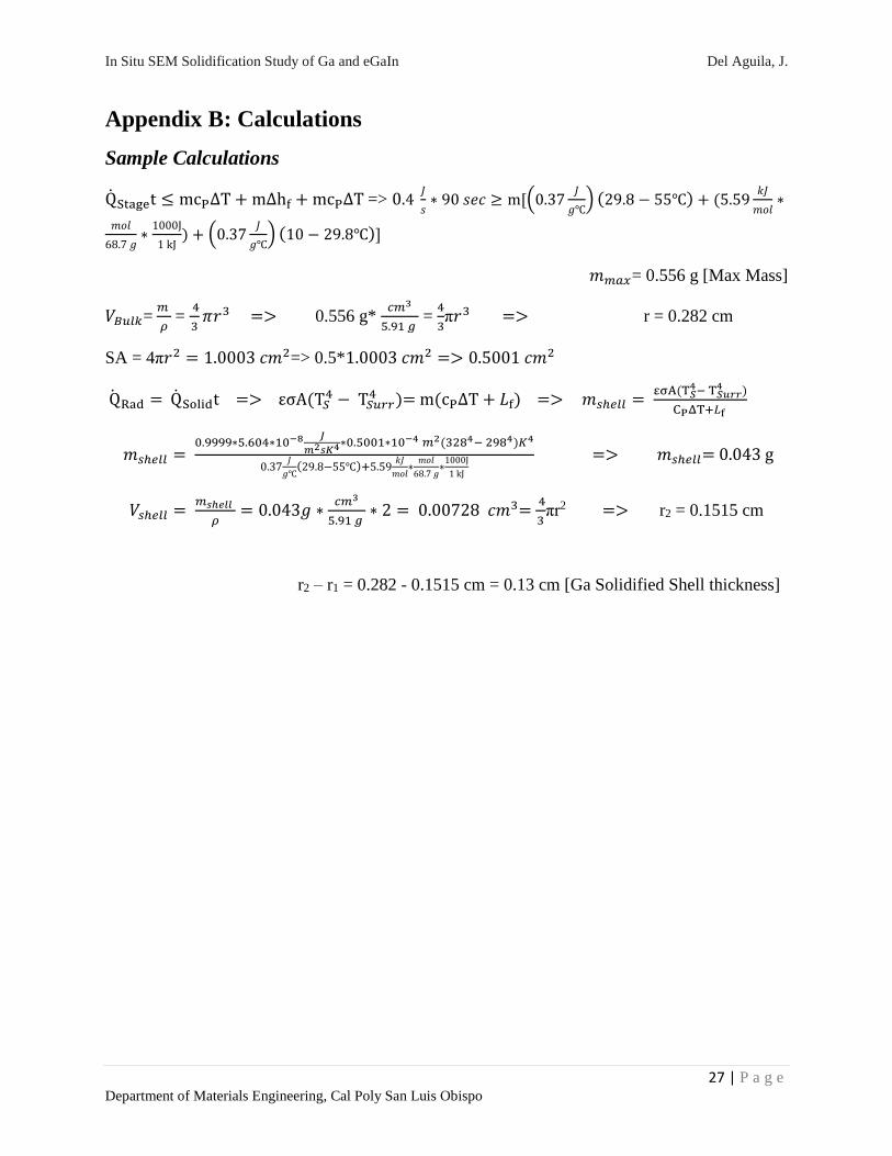
observed in Figure 12 was determined as 0.043 g (See appendix B for calculations). This ignores
the fact that the composition and thermal properties of the surface are different than the bulk
solid.
Considering Figure 13, this sequence of micrographs depicts a video recording of solidification
of eutectic mushy microstructure taking place inside of a cavity. Voids at the center of the mushy
zone interacted with the e beam and began to coalesce and open until reaching the boundaries of
the cavity. Looking through the hole, a dark liquid phase most likely rich in Ga can be seen.
After a 15-minute recording, the same zone becomes grey and can be said to have solidified. The
differences between Figure 12 and Figure 13 can be attributed to the degree of superheating the
specimen were subject to prior to being imaged. The specimen heated and etched at a higher
temperature formed more prominent microstructural features however could not be captured in
time, whereas the ladder could.

In Situ SEM Solidification Study of Ga and eGaIn Del Aguila, J.
21 | P a g e Department of Materials Engineering, Cal Poly San Luis Obispo
IV. Conclusions
The purpose of this study was to investigate whether HVSEM and Peltier Cooling could be used
for monitoring the microstructural evolution of liquid metals. Equilibrium cooling studies of Ga
and eGaIn show evidence of solidification through video recordings. The present study showed
the following:
• Prevalence of a metallic oxide layer on cast samples prevents microstructural analysis t
must be reduced through sample preparation.
• The application of 3% HCl solution was successful in reducing the oxide layer of metal
spheres that decreased the surface tension and embrittled the surface.
• Etched and air-cooled Ga samples show breaking of oxide surface due to volume
expansion of solid to liquid transition.
• Bubble cavitation and gaseous diffusion at specimen surface generates cavities that act as
viewing windows for the underlying microstructure in Ga and GaIn samples.
• Rapid solidification of surface is sensitive to superheat temperature and can occur before
the onset of imaging so TSuperheat should be chosen with caution.
Recommendations
• Use of ESEM with a GSED detector to prevent contamination of SEM chamber via off
gassing and allow for more realistic studies.
• Use of EDS to do a compositional analysis of the surface as solidification is taking place.
• Modify the heat transfer model to account for e beam/surface interaction as well as the
difference in shell composition.
• Use a probe to crack the surface prior to imaging or while in the chamber.

In Situ SEM Solidification Study of Ga and eGaIn Del Aguila, J.
22 | P a g e Department of Materials Engineering, Cal Poly San Luis Obispo
V. References
1 A. Bogner, P.-H. Jouneau, G. Thollet, D. Basset, C. Gauthier, A History of Scanning Electron
Microscopy Developments: Towards “wet-STEM” imaging, In Micron, Volume 38, Issue 4,
2007, Pages 390-402
2 J. Goldstein, D.E Newbury, J.W Colby, H. Yakowitz, E. Lifshin, J.R. Coleman, Practical
Scanning Electron Microscopy: Electron and Ion Microprobe Analysis. (1975) Plenum Press,
New York.
3 Z. Weilie, R. P. Apkarian, Z. L. Wang, D. Joy, Scanning Electron Microscopy for
Nanotechnology. (2006) Springer
4 G.D, Danilatos, V. Robinson, Principles of Scanning Electron Microscopy at High Specimen
Pressures. Scanning, Issue 2, (1979), Pages 72-82.
5 Del Aguila, J. Literature Review on SEM fundamentals, Cal Poly San Luis Obispo,
Department of Materials Engineering, (2017).
6 Esmaily, N. et al., On the Capability of in-situ Exposure in an Environmental Scanning
Electron Mcroscope for Investigating the Atmospheric Corrosion of Magnesium,
Ultramicroscopy, Volume 153, (2015), Pages 45-54.
7 A.J Smith, In Situ Environmental Scanning Electron Microscopy (ESEM) of Semi-Solid
Samples, Solid State Phenomena, Volumes 116-117, (2006), Pages 700-703.
8 Naman M. D. Solidification, Mechanical Eng. Dept. Gandhinagar Institute of Technology.
MATERIAL SCIENCE & METALLURGY. Chapter 1
9 O’Hare, R. Materials Kinetics Fundamentals: Principals, Processes, and Applications. Wiley
Publishing, Hoboken NJ, (2015), Ch.6-7.
10 A. Tang, D. Sarang. “Chemistry of Gallium (Z=31).” Chemistry LibreTexts, Libretexts, web.
Accessed 21 July 2016.
11 Lenntech.com, Periodic Elements: Gallium, web. Accessed 23, Nov 2017.
12 Properties of Pure Metals, Properties and Selection: Nonferrous Alloys and Special-Purpose
Materials, Vol 2, ASM Handbook, ASM International, (1990), Pages 1099–1201.
13 Mohammed, M. G., A Study of Eutectic Gallium Indium Liquid Metal in Microsystems and
Interfaces. Doctoral Dissertation, Department of Chemical Engineering, University of Cairo,
Egypt.

In Situ SEM Solidification Study of Ga and eGaIn Del Aguila, J.
23 | P a g e Department of Materials Engineering, Cal Poly San Luis Obispo
14 Burdakin et al., Melting Points of Gallium and of Binary Eutectics with Gallium Realized in
Small Cells. Vol 45, Issue 1, Metrologia (2008), Pages 75 – 82.
15 Kolman, D. G., Bingert, J. F., & Field, R. D. The Microstructural, Mechanical, and Fracture
Properties of Austenitic Stainless Steel Alloyed with Gallium. NACE International (2003).
16 M. D. Dicky, R. C. Chiechi, R. J. Larsen, E. A. Weiss, D. A. Weitz, and G. M. Whitesides,
Eutectic gallium-indium (EGaIn): A liquid metal alloy for the formation of stable structures in
microchannels at room temperature, Adv. Funct. Mater. 18, 1097–1104 (2008). 11R.
17 J. Larsen, M. D. Dickey, G. M. Whitesides, and D. A. Weitz, Viscoelastic properties of oxide-
coated liquid metals, J. Rheol. 53(6), 1305–1326 (2009).
18 Zinkevich, M. and Aldinger, F., Thermodynamic Assessment of the Gallium‐Oxygen System.
Journal of the American Ceramic Society (2004), Vol 87, Pages 683-691.
19 Xu, Q., Oudalov, N., Guo, Q., Jaeger, H. & Brown, E. Effect of oxidation on the mechanical
properties of liquid gallium and eutectic gallium-indium. Phys. Fluids (2012), Vol 24,
20 Young, D.A. Phase diagrams of the elements. United States Department of Energy (1975),
Technical Report.
21 Anderson, T. & Ansara, I. The Ga-In (Gallium-Indium) System. JPE (1991) Vol 12, Issue 64.
Pages 64-72.
22 CRC Handbook of Metal Etchants, CRC Press: Boca Raton, FL, (1991)
23 Bergman, T., Fundamentals of Heat and Mass Transfer 7th Edition. Wiley Publishing,
Hoboken NJ, (2015), Ch.1,12.
24 <Ga properties> CES Edupack 2017/The Elements/Gallium
25 Cardenas-Garcia, G., Design and Construction of a gallium fixed-point blackbody at
CENAM. Revista Mexicana de Fısica (2015), Vol 61, Pages 74–76 .
26 CRC Handbook of Chemistry and Physics, 92nd ed.; CRC Press: Boca Raton, FL, (2012)
27 Stepanov, S.I. & Nikolaev, V.I. & Bougrov, V.E. & Romanov, Alexey. (2016). Gallium
oxide: Properties and applications - A review. Issue 44. Pages 63-86.

In Situ SEM Solidification Study of Ga and eGaIn Del Aguila, J.
24 | P a g e Department of Materials Engineering, Cal Poly San Luis Obispo
Appendix A: Literature Review
Electron-Specimen Interactions - Signals
Inelastic and Elastic Scattering
Fundamentally, an SEM produces a high number of electron signals by scanning a focused
electron beam across a material surface. These signals are electron-specimen interactions that
carry information about the nature of the specimen and are responsible for the formation of an
image. These interactions are referred to as scattering and are divided into two general
categories: elastic and inelastic scattering interactions. Elastic scattering results from the
deflection of the incident electron beam by the nucleus of an atom or by outer shell electrons
carrying a similar energy as the beam4. Incident electrons that are elastically scattered through
angles greater than 90˚ are called backscattered electrons (BSEs), and generate a signal that can
be used to form an image. Inelastic scattering results from the transfer of energy between the
incident electron and the atoms and electrons of a sample2. Excitation of the electrons through
inelastic scattering ionizes a specimen surface and leads to the generation of secondary electrons
(SEs). Secondary electrons are defined as low energy electrons, typically below 50 eV (electron
volts) and provide the highest spatial resolution images6. Secondary electron and backscattering
signals are the most commonly used to render useful images of specimen in modern SEM
technology.
Detecting Electron-Specimen Interactions with Scintillation Detectors
Secondary Electron Detectors
In 1960, Everhart and Thornley optimized a device that could detect SEs and quickly advanced
the field of SEM instrumentation. The detector consisted of a positively biased grid surrounded
by a Faraday cage to collect low energy electrons emitted from the specimen surface, a
scintillator to convert them to light, and a light-pipe to transfer the light directly to a
photomultiplier tube8. This device became known as an Everhart and Thornley Detector (ETD)
and was incorporated into the first commercial SEM – the Cambridge Scientific Instrument in
1963 by Peace and Nixon9. Modern SEMs such as the FEI Quanta 200 come standard with an
ETD and have the option of equipping auxiliary detectors such as BSD, and GSEDs used in
ESEM mode that are specialized variations of ETDs. The SEM model used to carry out the
proceeding experiment includes an ETD and BSD.
In principal, ETDs receive all the electronic signals previously described but only SEs and BSEs
are processed to form an image. The image formation process is therefore dependent on
efficiency of an ETD to collect SEs and BSEs. The efficiency of ETDs is determined by the
choice of scintillation material, the magnitude and direction of the applied voltage on the
Faraday cage, and the relative position of the detector with respect to the specimen3.
The scintillator material choice plays a large role in the efficiency of an ETD because it is what
emits light when struck by excited electrons. SEs are inherently low in energy and can’t activate
the scintillator so the biased grid carrying a voltage on the order of tens of kilovolts helps to

In Situ SEM Solidification Study of Ga and eGaIn Del Aguila, J.
25 | P a g e Department of Materials Engineering, Cal Poly San Luis Obispo
accelerate these electrons to a high enough energy2. The magnitude and sign of the Faraday cage
also plays a crucial role in ETD efficiency because it is what attracts SEs to the vicinity of the
grid. For instance, if the bias is kept constant at 12 kV and the Faraday cage is set to -50V, then
only BSEs will be collected by the detector. On the other hand, if the Faraday cage bias is set to
+250 V, then both signals will be detected, and the collection of SEs will be the highest2. This
however is no longer an issue since BSEs can be detected by a solid-state BSDs, so ETDs can be
used primarily for SE detection. Lastly, the position of an ETD can vary largely with respect to
the surface of the observed specimen and is determined by what surface topographical features
an operator wants to observe. This highlights a key application of ETDs such that they are used
to render topographical images under the specimen surface. The depth that can be viewed
increases proportionally with accelerating voltage.
Backscattered Electron Detectors
The electronic signals that are detected by ETDs and BSDs are responsible for the type of
image that an SEM forms. Additionally, the way the image appears is a function of contrast
mechanisms that arise from different material properties such as atomic number, surface
topography, and crystalline orientation. To be able to interpret SEM micrograph data generated
from different (or a combination of) detectors and hence electronic signals, a brief discussion
about these mechanisms follows.
Contrast Mechanisms – Topography, Atomic Number, and Electron Channeling
Channeling Contrast
A governing contrast mechanism that produces such sharp images is known as electron
channeling contrast effect. The effect arises because of the differing atomic packing densities
along different crystallographic directions2. When an electron beam propagates through the
lattice, it passes between rows of atoms thereby forming channels. The degree to which an
incident electron beam normal to a surface penetrates a crystalline material depends on the angle
of incidence. Incident beams with high tilt angles will penetrate the crystalline material at larger
interatomic distances. The probability of electrons escaping from deep channels is lower than
those only interacting with the surface2. Likewise, only the signals generated from channeling
effects near the surface contribute significantly to the overall contrast of a micrograph.
Topography Contrast
Contrast of topographical features allow for edges, corners, steps, and surface roughness to be
distinguishable in great detail2. The degree to which the surface features are shadowed or
highlighted depend on the relative position of the detector with respect to the surface and the
inclination of the topographical features of the specimen surface with respect to the incident
beam. It has been found that surfaces containing facets generate more SEs when the tilt angle is
high. It is common to reveal the microstructure of specimen prior to imaging to maximize
topographical contrast.

In Situ SEM Solidification Study of Ga and eGaIn Del Aguila, J.
26 | P a g e Department of Materials Engineering, Cal Poly San Luis Obispo
Atomic Number Contrast
Another contrast mechanism used to render characteristic SEM micrographs is atomic number
contrast. This mechanism arises because of a different number of electrons leaving a specimen at
one region compared to another. This is easily understood by considering a slow cooled
multiphase alloy that develops distinct phases separated by grain boundaries. The electron-
specimen interaction will vary between phases because they are composed of different materials,
have different atomic numbers, and hence a different electronic distribution. Regions composed
of elements with high atomic numbers appear dark while regions with low atomic numbers
appear white in an ETD image and the opposite for an image formed by a BSD2.
The contrast characteristics of SEM micrographs is thus an ensemble of each of these contrast
mechanisms. The dominance of one mechanism over another highly depends on the material
system to be investigated. Interpretation of SEM images is therefore reliant on understanding the
signals and contrast mechanisms that render an image. The detectors used also plays a crucial
role in being able to obtain quality information.
In Situ SEM Solidification Study of Ga and eGaIn Del Aguila, J.
27 | P a g e Department of Materials Engineering, Cal Poly San Luis Obispo
Appendix B: Calculations
Sample Calculations
Q̇Staget ≤ mcPΔT + mΔhf + mcPΔT => 0.4 𝐽
𝑠∗ 90 𝑠𝑒𝑐 ≥ m[(0.37
𝐽
𝑔℃) (29.8 − 55℃) + (5.59
𝑘𝐽
𝑚𝑜𝑙∗
𝑚𝑜𝑙
68.7 𝑔∗
1000J
1 kJ) + (0.37
𝐽
𝑔℃) (10 − 29.8℃)]
𝑚𝑚𝑎𝑥= 0.556 g [Max Mass]
𝑉𝐵𝑢𝑙𝑘= 𝑚
𝜌 =
4
3𝜋𝑟3 => 0.556 g*
𝑐𝑚3
5.91 𝑔 =
4
3π𝑟3 => r = 0.282 cm
SA = 4π𝑟2 = 1.0003 𝑐𝑚2=> 0.5*1.0003 𝑐𝑚2 => 0.5001 𝑐𝑚2
Q̇Rad = Q̇Solidt => εσA(T𝑆4 − T𝑆𝑢𝑟𝑟
4 )= m(cPΔT + 𝐿f) => 𝑚𝑠ℎ𝑒𝑙𝑙 = εσA(T𝑆
4− T𝑆𝑢𝑟𝑟4 )
CPΔT+𝐿f
𝑚𝑠ℎ𝑒𝑙𝑙 = 0.9999∗5.604∗10−8 𝐽
𝑚2𝑠𝐾4∗0.5001∗10−4 𝑚2(3284− 2984)𝐾4
0.37𝐽
𝑔℃(29.8−55℃)+5.59
𝑘𝐽
𝑚𝑜𝑙∗
𝑚𝑜𝑙
68.7 𝑔∗
1000J
1 kJ
=> 𝑚𝑠ℎ𝑒𝑙𝑙= 0.043 g
𝑉𝑠ℎ𝑒𝑙𝑙 = 𝑚𝑠ℎ𝑒𝑙𝑙
𝜌= 0.043𝑔 ∗
𝑐𝑚3
5.91 𝑔 ∗ 2 = 0.00728 𝑐𝑚3=
4
3πr2 => r2 = 0.1515 cm
r2 – r1 = 0.282 - 0.1515 cm = 0.13 cm [Ga Solidified Shell thickness]