IN SITU DIFFERENTIAL SCANNING ELECTRON ... J. Res. 47(1993) 163-183 IN SITU DIFFERENTIAL SCANNING...
21
Philips J. Res. 47 (1993) 163-183 IN SITU DIFFERENTIAL SCANNING ELECTRON MICROSCOPY DESIGN AND APPLICATION by A. SICIGNANO Philips Laboratories, Briarclijf Manor. NY. USA Abstract This paper isa review of work on insitu differential imaging in the scanning electron microscope. In the SEM elementary contrast enhancement is obtained by either of two methods, black level suppression, or differential imaging. In this paper we are concerned with the second method. Differen- tial imaging as applied to SEM images is typically achieved by either using a selective electronic filtering circuit (time sensitive) on the video signals, or after acquisition of a digital image by the application of special kernel operators (post processing). The method described in this paper is capable of generating in situ SEM differential video signals from local sample features. Important characteristics of this method are improved sample feature boundary sensitivity, the suppression of often large background signals, and the capability ofperforming critical pattern-feature-alignment before feature measurements. Examples of results obtained applying this technique to the generic field of scanning electron microscopy, and to the measurement of critical dimensions of integrated circuits are presented. Implementation to commercially available SEMs (this work was done using a Philips 535-SEM) can be accomplished in a variety of modes. Keywords: critical dimensions, in situ differential imaging, integrated circuits, metrology, SEM. 1. Introduetion This paper is a review of work on in situ differential imaging in the scanning electron microscope (SEM)I-4). In conventional SEM imaging, the video signals are first detected at a secondary electron detector (SED) and then passed through a series of video amplifiers to obtain linear gain and DC offsets. 6). The contrast and brightness controls are frequently less adequate for the imaging of low contrast sample features, especially if a large DC offset (background) is a component of the video signal. We want to concentrate on the boundaries of features which are often of prime interest in many materials Philips Journul of Research Vol.47 Nos. 3-S 1993 163
Transcript of IN SITU DIFFERENTIAL SCANNING ELECTRON ... J. Res. 47(1993) 163-183 IN SITU DIFFERENTIAL SCANNING...
Philips J. Res. 47 (1993) 163-183
IN SITU DIFFERENTIAL SCANNING ELECTRONMICROSCOPY DESIGN AND APPLICATION
by A. SICIGNANO
Philips Laboratories, Briarclijf Manor. NY. USA
AbstractThis paper is a review of work on in situ differential imaging in the scanningelectron microscope. In the SEM elementary contrast enhancement isobtained by either of two methods, black level suppression, or differentialimaging. In this paper we are concerned with the second method. Differen-tial imaging as applied to SEM images is typically achieved by either usinga selective electronic filtering circuit (time sensitive) on the video signals, orafter acquisition of a digital image by the application of special kerneloperators (post processing). The method described in this paper is capableof generating in situ SEM differential video signals from local samplefeatures. Important characteristics of this method are improved samplefeature boundary sensitivity, the suppression of often large backgroundsignals, and the capability ofperforming critical pattern-feature-alignmentbefore feature measurements. Examples of results obtained applying thistechnique to the generic field of scanning electron microscopy, and to themeasurement of critical dimensions of integrated circuits are presented.Implementation to commercially available SEMs (this work was doneusing a Philips 535-SEM) can be accomplished in a variety of modes.Keywords: critical dimensions, in situ differential imaging, integrated
circuits, metrology, SEM.
1. Introduetion
This paper is a review of work on in situ differential imaging in the scanningelectron microscope (SEM)I-4). In conventional SEM imaging, the videosignals are first detected at a secondary electron detector (SED) and thenpassed through a series of video amplifiers to obtain linear gain and DCoffsets. 6). The contrast and brightness controls are frequently less adequate forthe imaging of low contrast sample features, especially if a large DC offset(background) is a component of the video signal. We want to concentrate onthe boundaries of features which are often of prime interest in many materials
Philips Journul of Research Vol.47 Nos. 3-S 1993 163

A. Sicignano
studies. Examples of this application include, in particular, stereology and themeasurement of critical dimensions (CDs) of integrated circuits (ICsr' 8). Foreach of these applications improved detection of sample features is needed tolocate feature edges unambiguously with a high sensitivity and accuracy, andsimultaneously to suppress unwanted background signals.
Precision metrology of the various submicron features in the IC world is aprime goal for many existing efforts in the field of SEM9
-11
). The basic drivingforce behind such an intense interest remains the ever increasing need formetro logies displaying a number of important characteristics.
Chief amongst these are high resolution and contrast, reliability, existingsoftware and hardware support, and ease of interpretation of the results. Thetrend in the IC industry is toward continued reduction of CDs. The SEM is atpresent a highly developed tool for metrology of CDs of 0.5 Jlm and smaller.
The enhancement of feature edges is often attempted in the following twoways: (1) using an electronic circuit to provide frequency discrimination/filter-ing (time domain discrimination) or, (2) the post processing of digitallyacquired and stored images through the application of various kernelconstructs"), Electronic differentiation is a time derivative phenomenon.Accordingly, the relationship between electronically differentiated signals andthe spatial variations on the sample is directly dependent on the e-beam scanspeed. Since there are many situations where the lack of sufficient signal/noise(S/N) necessitates slow scanning speeds, electronic differentiation cannot be auniversal solution to the problem of contrast, as this type of differentiation isunsuitable for slow scanning speeds. Even in those cases where one cansuccessfully perform electronic differentiation. the resulting signal is only arepresentation of the x-derivative of the sample, because we are actuallyfrequency filtering the video signal, not monitoring local variations in thesample (by detecting local changes in the signal). There are important cases inwhich this constraint imposes a severe limitation. Computer-aided post-processing of the digitized images, on the other hand, obviously prolongs theprocess of obtaining the final image. Furthermore, it should be stressed thatthe outcome of such an exercise essentially suffers from the limitations of theoriginally acquired image, such as the increased sensitivity of features alongthe primary x-scan direction. In a conventional SEM e-beam rastering, thee-beam continuously traverses a horizontal path (x-scan line), while in thevertical direction there is a discontinuous sampling of features (discrete stepsbetween x-scan lines).
This review paper describes the design and application of an in situ differen-tial imaging technique to general electron microscopy as well as metrology. Afundamental characteristic of this method is that it directly effects an enhance-
164 Philips Journal of Research Vol.47 Nos.3-5 1993

In situ differentlal scanning electron microscopy
Fig. I. Schematic overview comparing conventional SE signal with rectified in situ differentialsignalon two types of samples: a) a sample with varying topography but uniform composition;b) a flat sample of varying composition.
ment of feature boundaries, by providing a true differential video signaloflocal sample features. Since differentiation increases image clarity and sensitiv-ity to subtle variations, for a given SEM resolution, the accuracy of featuremeasurements is expected to increase.These concepts are schematically depictedin fig. I, where a comparison is made between a conventional and a rectified-differential secondary electron (SE) video profile of two types of samples: a) asample of uniform composition but a varying topography, and b) a samplewith no topography but varying composition (the center of the sample havinga different composition than the edges).
2. Principle
The basic aspects of the differential imaging technique are best describedwith reference to fig. 2. In its simplest embodiment, the method calls for asinusoidal alteration of the relative position of the e-beam, to the sample, ata given point. This can be effected by superimposing a high frequency, lowamplitude, signalon the SEM scan generation current (normal scan-coildeflection signal). The video signalsdetected at the secondary electron detectorare fed into a multichannel frequency spectrum analyzer and the in situdifferential video signal (centered around the deflection frequency {Is}) isextracted. The bandwidth (BW)ofthe in situ differential signal can be adjustedfor specific applications and a range of 10-100 Hz is typical. An alternative
c..>»:
varying topographyuniform composition
Philips JournnI of Research VOl.47 Nos.3-5 1993
bI' I I s.r>:JLJLnllt sample
varying yield
165

A. Sicignano
vd.fI.ctlonIIdd.d to
norm.1 scan ~ II
flInt
Fr.Qu.ncy Sp.ctrum "n.lyzersign.' Int.nslty vs fr.Qu.ncy
dlff.rentl.1slgn.1
In Situ diU.Imeg. dlSPI.y
Fig. 2. Schematic diagram of the system configuration showing how the extra deflection is addedto conventional SEM, and how ill situ differential signal is extracted.
method to using a frequency spectrum analyzer is employing a narrow passfilter centered atJ., with an adjustable BW.
In the absence ofa local variation (materialor geometric) on the sample, theresulting video signal consists only of a DC signal, which is representative ofthe general SE signal yield (for the SE mode). However if a variation does existon the sample, then the video signal will include a term, centered on the I.,which is a measure of the differential yield. If the deflection frequency isarranged so that the e-beam performs at least two deflection cycles (over thesame region of the sample) during a given pixel acquisition time, the differen-
166 Philips Journalof Research Vol.47 Nos. 3-5 1993
In situ differential scanning electron microscopy
ti al signal becomes independent of the scan speed. This enables the techniqueto be used with low scan speeds to achieve sufficient SIN.
3. Theory of operation
3.1. Case 1:material variation without topography
To understand the theory of operation, consider first a flat object, whichconsists oftwo different materials with a well-defined boundary between them(see fig. lb). We can use the analysis as applied to the SE emission mode,although the technique, and the analysis are equally applicable to other SEMimaging modalities, including backscattered electrons (BSE). In the simplestcase, we can represent the video signal output of a conventional SEM for anygiven point in a semi-infinite material, in the SE mode, by")
(1)
where 0 is the secondary electron yield, and cP is the sample tilt angle. Here, wehave assumed a zero azimuth angle between the sample and secondary electrondetector (SED). In the differential mode, with the local x-deflection superim-posed on the electron beam x-scan signal, at the moment when the center ofthe local e-beam deflection is coincident with the boundary of the twomaterials, we have
(2)
where om is the mean secondary electron yield of the two materials, /).0 is halfthe difference in the secondary electron yield, and CVs is the added localdeflection frequency. In this expression, we have included only the terms inDC, and the fundamental frequency. Higher harmonics are present because ofthe convolution of the e-beam spot size, and the structure. However, thissimplified form of eq. (2) is adequate for our present purposes. Noting that thedesired signal is obtained at Is (the additional in situ differential modulationfrequency), we have
(3)
that is, the signal obtained at Is is proportional to the differential secondaryelectron yield.
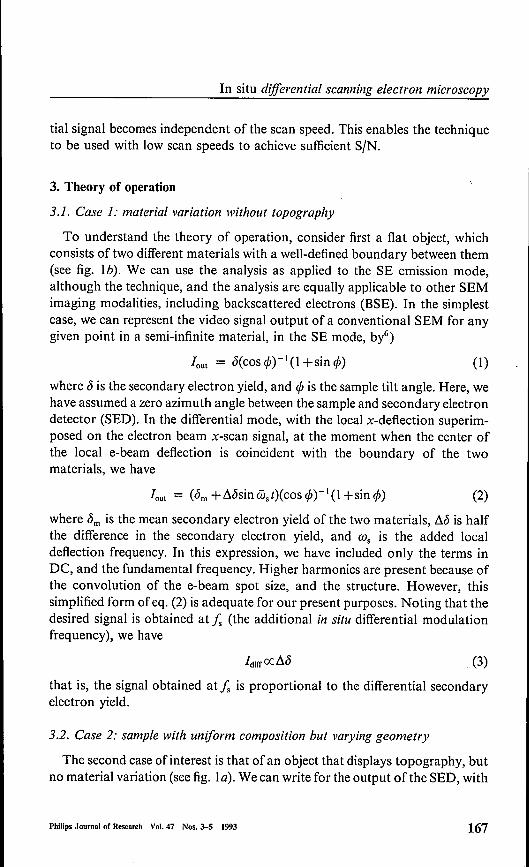
3.2. Case 2: sample with uniform composition but varying geometry
The second case of interest is that of an object that displays topography, butno material variation (see fig. la). We can write for the output ofthe SED, with
Philips Journalof Research Vol. 47 Nos. 3-5 1993 167

A. Sicignano
the local beam deflection superimposed on the x-scan, the expression
Ioul = c5[cos(cPa + LlcPsinwst)]-I [1+ sin (cPa + LlcPsinrost)] (4)
where cPa represents the general sample tilt, and LlcP is the local variation in thistilt due to topography. Once again, (j denotes the secondary electron yield ofthe sample. For small LlcP the expression reduces to
(5)
where JI is the first-order Bessel function of the first kind. The differentialsignal, obtained at!., is given by
IOUI = 2(j[tan cPa][JI (LlcP)] (6)
Therefore, for small LlcP, we have
(7)
that is, the output at!. is proportional to the local slope of the structure.The additional sinusoidal deflection signals (!.) used were in the 50-500 kHz
range, with an amplitude adjusted to result in a local e-beam deflection suchthat the displayed image resolution is not degraded (local deflection ~ pixelwidth). The amplitude is also adjusted for the magnification being used. If theentire surface within the e-beam raster area is to be interrogated, then theamplitude of the local deflection is increased with decreasing magnification.Figure 3 shows the horizontal (x-scan) mode of e-beam deflection in which thein situ differential deflection is added to the normal SEM x-scan deflection. Inthis mode we are sensitive to feature boundaries along the vertical (y) direction(superposition of a small amplitude sinusoidal deflection on the x-scan deflec-tion signal). Figure 4 shows the results of superimposing a periodic local(differential) deflection on the e-beam (normal deflection) position.
The different methods of embodiments for the in situ differential more aregiven in Table I. Feature edge detection direction can be selected by superim-posing the local e-beam deflection signal in a variety of modes or by themechanical displacement ofthe sample during normal e-beam rastering. Whenequal amplitude quadrature signals are added to the x and y deflection signals,the result is an in situ differential video signal equally sensitive to featureboundaries in all directions of the x-y (raster) plane.It should be noted that Balk and co-workers'è 13) have previously used a
similar technique, in one direction, and have presented a number of linescans.However the basic driving force behind their work appears to have been togenerate an AC signal (which could then be detected by a lock-in amplifier) ingeneral, and to suppress the DC bias current in obtaining electron-beam-
168 Philips Journalof Research Vol.47 Nos.3-5 1993

Philips Journal of Research Vol.47 Nos. 3-5 1993 169
In situ differential scanning electron microscopy
Digital X scan with onedimension deflection
t _5,5
·5,5.5_5
_5. 5
_5-5_5
S
se ..n disbne. _
••Fig. 3. The x-scan mode of operation in the ill situ differential SEM, using added deflection thex-direction.
urrec tmn of una-seene-beam
IIII
local uet lec t ren III
obJect
Fig. 4. Effect of added deflection on the position of the beam (highly exaggerated).
A. Sicignano
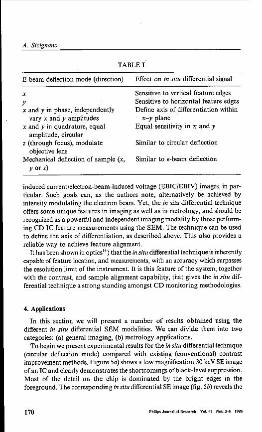
TABLE I
E-beam deflection mode (direction) Effect on in situ differential signal
x Sensitive to vertical feature edgesSensitive to horizontal feature edgesDefine axis of differentiation withinx-y plane
Equal sensitivity in x and y
yx and y in phase, independently
vary x and y amplitudesx and y in quadrature, equal
amplitude, circularz (through focus), modulate
objective lensMechanical deflection of sample (x,
y or z)
Similar to circular deflection
Similar to e-beam deflection
induced current/electron-beam-induced voltage (EBIC/EBIV) images, in par-ticular. Such goals can, as the authors note, alternatively be achieved byintensity modulating the electron beam. Yet, the in situ differential techniqueoffers some unique features in imaging as well as in metrology, and should berecognized as a powerful and independent imaging modality by those perform-ing CD IC feature measurements using the SEM. The technique can be usedto define the axis of differentiation, as described above. This also provides areliable way to achieve feature alignment.It has been shown in optics") that the in situ differential technique is inherently
capable of feature location, and measurements, with an accuracy which surpassesthe resolution limit of the instrument. It is this feature of the system, togetherwith the contrast, and sample alignment capability, that gives the in situ dif-ferential technique a strong standing amongst CD monitoring methodologies.
4. Applications
In this section we will present a number of results obtained using thedifferent in situ differential SEM modalities. We can divide them into twocategories: (a) general imaging, (b) metrology applications.To begin we present experimental results for the in situ differential technique
(circular deflection mode) compared with existing (conventional) contrastimprovement methods. Figure Sa) shows a low magnification 30 keY SE imageof an IC and clearly demonstrates the shortcomings of'black-level suppression.Most of the detail on the chip is dominated by the bright edges in theforeground. The corresponding in situ differential SE image (fig. Sb) reveals the
170 Philips Journal of Research Vol. 47 Nos. 3-5 1993
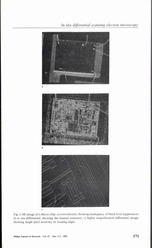
Philips Journalof Research Vol. 47 Nos. 3-5 1993 171
In situ differential scanning electron microscopy
b
c
Fig. 5. SE image ora silicon chip: a) conventional, showing inadequacy of black-level suppression;b) in situ differential, showing the internal structure; c) higher magnification differentlal image,showing single pixel accuracy in locating edges.

A. Sieignano
b
Fig. 6. BSE image of a patterned photoresist sample: a) differential by post-processing; b) in si/udifferential.
internal structure of the TC. Also note that variations within the bright edgesare also visible. So, the technique succeeds in imaging small variations in thesample, regardless of the background signal. Figure 5e) is a higher magnifica-tion inverted in situ differential image of the aluminum interconnect patternson the IC. This image was printed using a laser printer and demonstrates apowerful feature of the technique, the ability to determine the location of afeature edges with a single pixel accuracy.
At 1000 x magnification using a 512 x 400 image array size, I pixel =0.23,um x 0.23,um. Tf a feature must be measured with an accuracy > 0.2,um,either the magnification or the array size is be increased.
Post-processing of images has significant limitations in preserving the in-tegrity of the original signal information, as can be seen in figure 6a). Here the
172 Philips Journalof Research Vol. 47 Nos.3--5 1993
Philips Journalof Research Vol.47 Nos.3---5 1993 173
In situ differential scanning electron microscopy
b
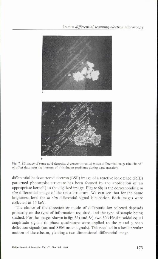
Fig. 7. SE image of some gold deposits: a) conventional; b) in situ differential image (the "band"of offset data near the bottom of b) is due to problems during data transfer).
differen tial backscattered electron (BSE) image of a reactive ion-etched (RJE)patterned photoresist structure has been formed by the application of anappropriate kernel") to the digitized image. Figure 6b) is the corresponding insitu differential image of the resist structure. We can see that for the samebrightness level the in situ differential signal is superior. Both images werecollected at IS keY.
The choice of the direction or mode of differentiation selected dependsprimarily on the type of information required, and the type of sample beingstudied. For the images shown in figs Sb) and Sc), two 50 kHz sinusoidal equalamplitude signals in phase quadrature were applied to the x and y scandeflection signals (normal SEM raster signals). This resulted in a local circularmotion of the e-bearn, yielding a two-dimensional differential image.
A. Sicignano
Figure 7a) shows an SE image of gold deposited on a silicon substrate. Thegold has "cracked" forming many intricate structures. Figure 7b) is the corres-ponding in situ differential image using z-modulation. For this purpose thesample was mounted on a small transducer and driven at 10 kHz, and thedifferential signal was extracted at this frequency. In fig. 7b) the only limitationto further resolving details on both the gold and the substrate is the displayresolution (the image array size, and/or display device). This method results ina two-dimensional differential image. Strong candidates for in situ differentialimaging include samples with very small variations on large backgrounds, andsamples with "soft" edges.
A unique feature of in situ differential imaging is that it allows the x and ydifferential signals to be simultaneously and independently collected. Figure8a) is an SE image of a silicon trench structure viewed in cross-section at 20keY. This image consists primarily of orthogonal edges. Figures 8b-c) are thecorresponding x and y in situ differential images. In this example a 50 kHzsignal was superimposed on the x-scan and a 20 kHz signal was superimposedon the y-scan. So we were able to obtain independently the x and y differentialsignals at 50 kHz and 20 kHz respectively.
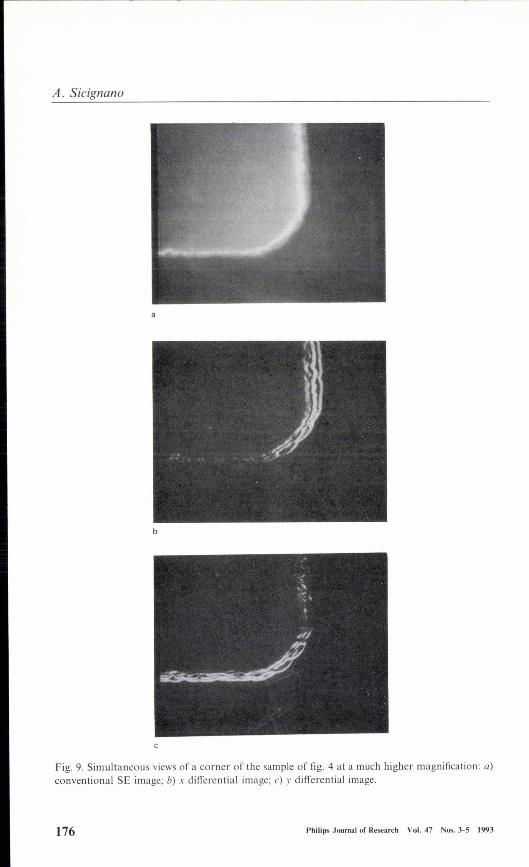
Figures 9a-c) are higher magnification images of the corners of the resiststructure shown in fig. 8. Figure 9a) is the conventional SE image. Figures9b-c) show the detail of standing wave patterns etched into the resist, using thesimultaneous differentiation technique, this detail is not revealed in the SEimage. This capability to acquire separately and simultaneously informationalong orthogonal directions should be important for metrology.
The metrology of CDs in ICs constitutes the second major category ofexperimental results discussed in this section. The SEM has been extensivelyused in this field, because ofits high resolution and depth of'field!"). A centralproblem common to any SEM determination of CDs in an IC is the samplealignment relative the e-beam scan axis. For precise measurement oflinewidthsit is necessary that the structure be orientated 90° to the direction of the e-beamscan. The in situ differential technique provides a direct way of accuratelyaligning the pattern (IC structure) to be measured. Ideal orientation can bedefined as one which gives rise to a maximum x derivative and a minimum yderivative of the linescan signal. To align a sample the simultaneous indepen-dent x and y differential signals are monitored as the pattern orientation isadjusted to maximize the former and minimize the latter.
After first using the alignment procedure outlined above, a series oflinescans were recorded from a number oftrack-like features (parallel trenchesof varying width etched in silicon).
Figure lOa) shows an SE linescan obtained from these features. Two impor-
174 Philips Journal of Research Vol.47 Nos.3-5 1993

Philips Journalof Research Vol. 47 Nos.3-5 1993 175
In situ differential scanning electron microscopy
b
Fig. 8. SE image of an etched pattern in silicon: a) conventional; b) in situ x differential; c)simultaneous y differential image. Note the selectivity in the images.
A. Sicignano
b
Fig. 9. Simultaneous views of a corner of the sample of fig. 4 at a much higher magnification: a)conventional SE image; b) x differential image; c) y differential image.
176 Philips Journalof Research Vol.47 Nos.3-5 t993

In situ differential scanning electron microscopy
Fig. 10. Linescan showing a series of trenches in silicon: a) conventional SE image; b) in situdifferential trace.
a
b
Philips Journal of Research Vol.47 Nos.3-5 1993
---
177
A. Sicignano
tant characteristics seen in this linescan are the characteristic SE edge enhance-ment, and a variable background signal due to the varying SE yield from thebottom of the Si trenches related to variation in trench width. The correspond-ing in situ differential image of the same feature is shown in fig. lOb). Thebackground signal has been suppressed. More importantly the linescan showsthe position of the maximum SE yield as well as maximum slope of the SEsignal with high accuracy (within a display pixel). Each peak in the differentiallinescan signal corresponds to the location of the maximum slope of the SEsignal, and each zero (between a pair ofpeaks) corresponds to location ofthemaximum in the SE signal.The linescans in figs I la-b) demonstrate the powerof the in situ differential technique in revealing extremely intricate detail of ICstructures. Figure lla) is an SE linescan of a single silicon structure formedbetween two etched trenches, and fig. lIb) is the x-scan differential ofthe samefeature. Each of the peaks in fig. lIb) corresponds to a local maximum in theslope of the SE linescan; these slope variations are themselves hardly notice-able in fig. lla). These results are particularly significant, because they forceus to define the concept of an edge for metrology purposes. The application ofin situ differential metrology can be of great potential value when used togetherwith computer algorithms written for such measurement purposes. Using analgorithm to detect the peak positions in the in situ differentiallinescan signalcan be done more critically than sensing level changes (defining a signallevelcorresponding to a feature boundary) in the normal SE linescan signal.The use of SE signals, while providing a superior SIN for imaging in the
SEM, may be less suitable in some applications where insulating features areimaged. Charge buildup may severely undermine the imaging process. In CDmetrology we may often be examining such objects as photoresist structures.One solution to this problem is the BSE model I). The in situ differentialtechnique can be used in this modality too. Figure 12a) shows a BSE (videosignal was inverted) linescan across an RIE patterned photoresist structure ona silicon substrate. Figure 12b) is the corresponding x differential BSElinescan, showing the exact positions of the BSE maximum slope as peaks indifferential signal.
For the last example, fig. 13a) shows an SE linescan across a raised siliconstructure between two trenches. Figure 13b) shows the two-dimensional dif-ferential linescan signalof the same feature obtained by modulating thee-beam focus. To achieve this we switched the modulation signalon and offwhile adjusting its amplitude, and noted that no observable change occurredin the normal SE linescan or image sharpness. The actual amount of z modula-tion was estimated to be O.OI-O.02,um.The in situ differential technique was
178 Philips Journal of Research Vol.47 Nos.3-S 1993

In situ differential scanning electron microscopy
a
Fig. 11. Linescan of a single Si track, formed between two consecutive trenches of the sample offig. 6: a) conventional 20 keY SE scan; b) in situ x differential trace. Note the emergence of subtlevariations in the structure.
Philips Journal of Research Vol. 47 Nos.3-5 1993 179

......L ........... ,"'' ~IIIL ...J.
l
--./A. Sicignano
a
-- "......31""
b
Fig. 12. BSE linescan of a photoresist track: a) conventional; b) in situ x differential.
180 Philips Journal of Research Vol. 47 Nos. 3-5 1993

In situ differential scanning electron microscopy
3pma
3 pmb
Fig. 13. SE linescan of an Si track formed as in fig. 7: a) conventional; b) differential imageobtained of the same sample by focus modulation.
Philips Journal of Research, Vol. 47 Nos.3-5 1993 181

182 Philips Journal of Research Vol.47 Nos. 3-S 1993
A. Sicignano
able to enhance subtle variations in the SE profile. The focus modulation asused in this example is essentially equivalent to x-differential imaging.
5. Conclusions
The design, theory of operation and various implementations of in situdifferential SEM have been described. The main shortcomings conventionalimage manipulation through black level suppression and electronic differentia-tion can be offset by generating a differential signal from the beginning,capable of accommodating both high and low bandwidths. Differentialimaging for metrology using the SEM can be accomplished in any direction(one dimension) or two-dimensional imaging. In addition, simultaneousderivatives along orthogonal directions can be acquired. The technique can beused for precise alignment of features before CD measurements.
Results on the application of the technique to general imaging and CDmetrology have been presented. It has been demonstrated that the techniqueis capable of achieving high accuracy in the location of sample edges. Thetechnique is also capable of allocating the full dynamic range to a displayedsignal for small sample feature variations. In metrology in situ differentialimaging is able to reveal the most subtle variations in sample features.
The accuracy with which the location of signal peak slope variations can bedetermined exceeds the resolution of the SEM as determined by its spot size.This technique is very flexible and its implementation to an existing SEM iseasily achieved.
Finally the technique can be employed as an acute focusing procedure bymonitoring the amplitude of the in situ differential signal while adjusting thee-beam spot size. Using small in situ deflection signals, sensitivity to detectionof a minimum spot size, and hence highly acute focusing can be achieved. Twoadvantages in using the in situ differential mode for focusing are the generationof sharply defined signals applicable to automated focusing algorithms, andthe ability to focus at lower magnifications without having to sense subtlechanges in the displayed image sharpness during focusing.
Acknowledgement
The author wishes to thank M. Vaez Iravani with whom the original workwas performed, and W. Friday, L.Herezeg and J. Beardsly for their assistancein providing data collection software and modifying the Philips 535-SEM forin situ deflection.

In situ differential scanning electron microscopy
REFERENCES
') A. Sicignano and M. Vaez Iravani, Design and application of in situ differential scanningelectron microscopy, Scanning Microsc .. 2 (I), 25 (1989).
') A. Sicignano and M. Vaez Iravani, Precision metrology ofintegrated circuit critical dimensionsusing in situ differential scanning electron microscopy, Scanning, 10,201 (1988).
J) A. Sicignano and M. Vaez Iravani, Metrology and practice of in situ differential scanningelectron microscopy, Scanning, 12,61 (1989).
4) A. Sicignano and M. Vaez Iravani, Quantitative linewidth measurement using in situ differen-tial SEM techniques, Proc. SPIE, 1261, 2 (1990).
') O.c. Wells, Scanning Electron Microscopy, McGraw-Hill, New York, 1974.6) L. Reirner, Scanning Electron Microscopy, Springer-Verlag, New York, Chap. 5, 1985.7) E.R. Weibel, Stereological Methods, Vol I, Chap. 6, Academic Press, London, 1974.8) S.O. Bennet, 1.T. Lindow and I.R. Smith, Scanning laser microscopy for integrated circuit
metrology, Annu. Meet. Opt. Soc. Am., Washington, DC, 1985.9) K. Monahan (ed.), Proc. SPIE Conf. on Integrated Circuit Metrology, Inspection and Process
Control, Vol 775, 1985.'0) S.O. Bennett, E.A. Peltzer and I.R. Smith, Ultraviolet confocal metrology, Proc. SPIE, 897,
75 (1988).") I. Hejna and L. Reimer, Backscartered electron multidetector system for improved quantitative
topographic contrast, Scanning, 9, 162 (1987).") L.I. Balk and E. Kubalek, Use ofphase sensitive-(Iock-in) amplification with scanning electron
microscopy, Beitr. Elektronmikroskop. Direktabb. Oberfl., 6, 551 (1973)13) L.I. Balk and E. Menzei Time resolved and temperature dependent measurements of electron
beam induced current (EBIC), electron beam induced voltage (EBIV), and cathodolumines-cence (CL) in the SEM, Scanning Electron Microscopy, IITRI, Chicago, IL, 1975, p. 447.
14) C.A. See and M. Vaez Iravani, Differential amplitude scanning optical microscopy: theory andapplications, Appl. Opt., 27, 2786 (1988).
15) K. Monahan (ed.), Proc. SPIE Conf. on Integrated Circuit Metrology, Inspection and ProcessControl, Vol. 775, SPIE, Bellingham, pp. 69-117 (1987).
Author
Alberl Sicignano: M.Sc. (materials science), Polytechnic, Brooklyn, NY,1982; Philips Electronic Instruments, Mahwah, Nl, 1967-1969; PhilipsLaboratories, Briarcliff, NY, 1969-. His early work related to electronbeam microprobe and STEM development, and the commercial intro-duetion of SEMs in the USA. At Philips Laboratories he worked one-bearn interactions with GaAs and ZnSe semiconductor materials, elec-trolytic and semiconductor capacitors, adhesion behavior of CRT emit-ter materials, failure analysis, and improved EDS-based analytical soft-ware and SEM imaging.Presently he is working on new W-mixed oxidemicrocomposite materials for lamp electrodes, and providing SEM-basedmaterials characterization for US business units.
Philips Journalof Research Vol. 47 Nos. 3-5 1993 183