i.MX Layout Recommendations - NXP … · i.MX Layout Recommendations Application Note, Rev 1.0 2...
20
Freescale Semiconductor Document Number: AN3951 Application Note Document Revision: 1.0 Date: 9/2009 © Freescale Semiconductor, Inc., 2009. All rights reserved. _______________________________________________________________________ i.MX Layout Recommendations by Networking and Multimedia Group Freescale Semiconductor, Inc. Austin, TX This document gives recommendations for PCB design to improve the behavior of the signals and create more robust designs. The i.MX31 is used as an example; however, the recommendations apply to the entire i.MX family of processors. 1 Mechanical The mechanical issues are considered before the PCB routing. These issues include the size of the board, the size and position of the mounting holes, the space between the housing, and the height of the components. 1.1 Outline The outline is the size and shape of the board. Use the import/export IDF command in the PCB tool to reduce outline creation problems such as special shapes or a large number of holes. This command can decrease the time for outline creation and increase accuracy of the outline drawing. Contents 1 Mechanical ................................................................ 1 1.1 Outline ................................................................... 1 1.2 Routing and Package Areas ........................................... 2 1.3 Height Restrictions ..................................................... 2 1.4 Mounting Holes ........................................................ 3 1.5 Fiducials ................................................................. 3 2 Placement .................................................................. 4 2.1 Critical Placement ...................................................... 4 2.2 Memories Module Placement ........................................ 5 2.3 Power Management Module Placement ............................ 6 2.4 Decoupling Capacitors ................................................ 8 3 Routing ..................................................................... 8 3.1 Stack-up.................................................................. 8 3.2 Fanout .................................................................... 9 3.3 Breakout ............................................................... 10 3.4 Critical Routing....................................................... 11 3.5 Power Planes ................................................................................. 17
Transcript of i.MX Layout Recommendations - NXP … · i.MX Layout Recommendations Application Note, Rev 1.0 2...
Freescale Semiconductor Document Number: AN3951 Application Note Document Revision: 1.0 Date: 9/2009
© Freescale Semiconductor, Inc., 2009. All rights reserved. _______________________________________________________________________
i.MX Layout Recommendations by Networking and Multimedia Group Freescale Semiconductor, Inc. Austin, TX
This document gives recommendations for PCB design to improve the behavior of the signals and create more robust designs. The i.MX31 is used as an example; however, the recommendations apply to the entire i.MX family of processors.
1 Mechanical
The mechanical issues are considered before the PCB routing. These issues include the size of the board, the size and position of the mounting holes, the space between the housing, and the height of the components.
1.1 Outline
The outline is the size and shape of the board. Use the import/export IDF command in the PCB tool to reduce outline creation problems such as special shapes or a large number of holes. This command can decrease the time for outline creation and increase accuracy of the outline drawing.
Contents
1 Mechanical ................................................................ 1 1.1 Outline ................................................................... 1 1.2 Routing and Package Areas........................................... 2 1.3 Height Restrictions ..................................................... 2 1.4 Mounting Holes ........................................................ 3 1.5 Fiducials ................................................................. 3
2 Placement .................................................................. 4 2.1 Critical Placement ...................................................... 4 2.2 Memories Module Placement ........................................ 5 2.3 Power Management Module Placement ............................ 6 2.4 Decoupling Capacitors ................................................ 8
3 Routing ..................................................................... 8 3.1 Stack-up.................................................................. 8 3.2 Fanout .................................................................... 9 3.3 Breakout ............................................................... 10 3.4 Critical Routing....................................................... 11 3.5 Power Planes................................................................................. 17

i.MX Layout Recommendations Application Note, Rev 1.0 2 Freescale Semiconductor
1.2 Routing and Package Areas
It is important to add the routing and keepin outlines which help reduce stress on the components and traces that are near the edge of the board, as seen in Figure 1. Table 1 shows the recommended distances, but actual values depend on application-specific requirements and tests.
Table 1 Recommended Outline Distances
Standard Minimum
Route Keepin 50 mil 20 mil Package Keepin 100 mil 50 mil
1.3 Height Restrictions
It is important to consider the maximum height of the components in a specific area. Placing these areas gives better control for the placement of taller components on restricted areas, as seen in Figure 2.
Figure 1 Routing and Package Areas
Package Keepin
Outline
Route Keepin

i.MX Layout Recommendations Application Note, Rev 1.0 Freescale Semiconductor 3
1.4 Mounting Holes
PCBs have mounting holes for components, housings, or assembly items. When placing these holes, take care with the distance to the components, shielding, and ground. Also, remember space for screws and other mounting devices used. The recommended air gap from a hole to a component is 80 mils.
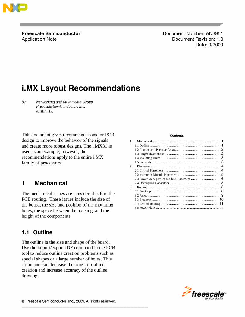
1.5 Fiducials
Fiducials are a type of pad that do not have an electrical connection. Fiducials help the assembly machines establish a reference. It is recommended to place at least two fiducials; however, it is best to include three fiducials. There are two types of fiducials as seen in Figure 3:
• Board fiducials establish an origin on the board for the components (on the top and bottom layer) during the placement by the pick and place machine
• Component fiducials are recommended for all fine pitch components
Figure 2 Height Restrictions
Package Keepout
Package Height on Top
Package Height on Bottom
i.MX Layout Recommendations Application Note, Rev 1.0 4 Freescale Semiconductor
Figure 3 Fiducials
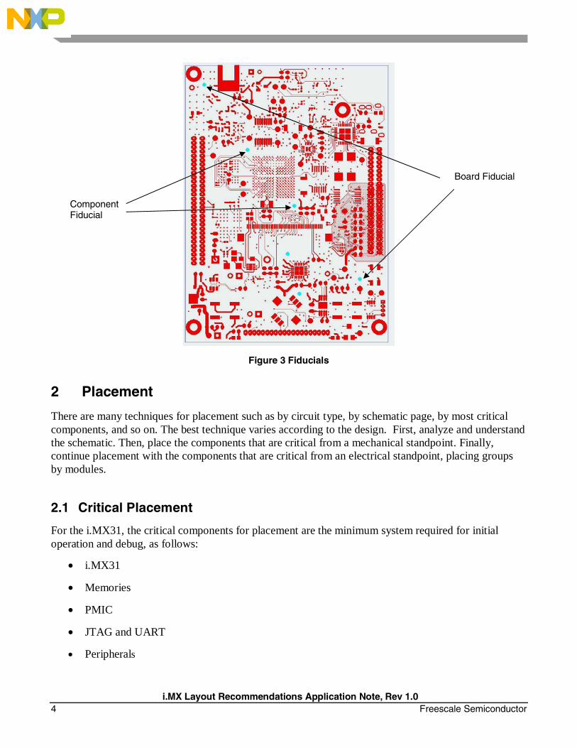
2 Placement
There are many techniques for placement such as by circuit type, by schematic page, by most critical components, and so on. The best technique varies according to the design. First, analyze and understand the schematic. Then, place the components that are critical from a mechanical standpoint. Finally, continue placement with the components that are critical from an electrical standpoint, placing groups by modules.
2.1 Critical Placement
For the i.MX31, the critical components for placement are the minimum system required for initial operation and debug, as follows:
• i.MX31
• Memories
• PMIC
• JTAG and UART
• Peripherals
Board Fiducial
Component Fiducial

i.MX Layout Recommendations Application Note, Rev 1.0 Freescale Semiconductor 5
2.2 Memory Module Placement
Using the i.MX31 PDK as a reference, the memory module includes the following devices:
• i.MX31
⎯ Pull-up/pull-down resistors
⎯ Decoupling capacitors
⎯ Crystal
• DDR
⎯ Decoupling/bypass capacitors
• NAND
⎯ Pull-up/pull-down resistors
⎯ Decoupling capacitors
Figure 4 Memory Placement Options
Figure 4 shows two options for the placement of the i.MX31 0.5-mm package and memory. In Option 1, the NAND Flash memory is next to the i.MX31, which allows shorter traces; however, the space in the bottom left corner is lost. Option 2 shows the NAND next to DDR memory, which has the opposite effect—longer traces but no lost space.
Option1 Option2

i.MX Layout Recommendations Application Note, Rev 1.0 6 Freescale Semiconductor
2.3 Power Management Module Placement
Using the i.MX31 PDK as a reference, the PMIC module includes:
• MC13783
⎯ Pull-up/pull-down resistors
⎯ Decoupling capacitors
⎯ Crystal
Figure 5 MC13783 Placement
Figure 5 shows the MC13783 in the middle of the PMIC module and the decoupling capacitors and pull-up/pull-down resistors placed around the MC13783. This configuration uses a large area of space and can be improved by moving the decoupling capacitors to the bottom side. The regulators are placed together, but they can be moved depending on restrictions on heat dissipation, power plane configurations, and height area.
The PMIC module also includes the following:
• Regulators and switchers
⎯ Pull-up/pull-down resistors
⎯ Decoupling capacitors
The inductors, capacitors, diodes, and power MOSFETs that are part of the buck-or-boost regulator configuration should be placed together to create a mini-module with good routing between them, such
PMIC Regulators
i.MX Layout Recommendations Application Note, Rev 1.0 Freescale Semiconductor 7
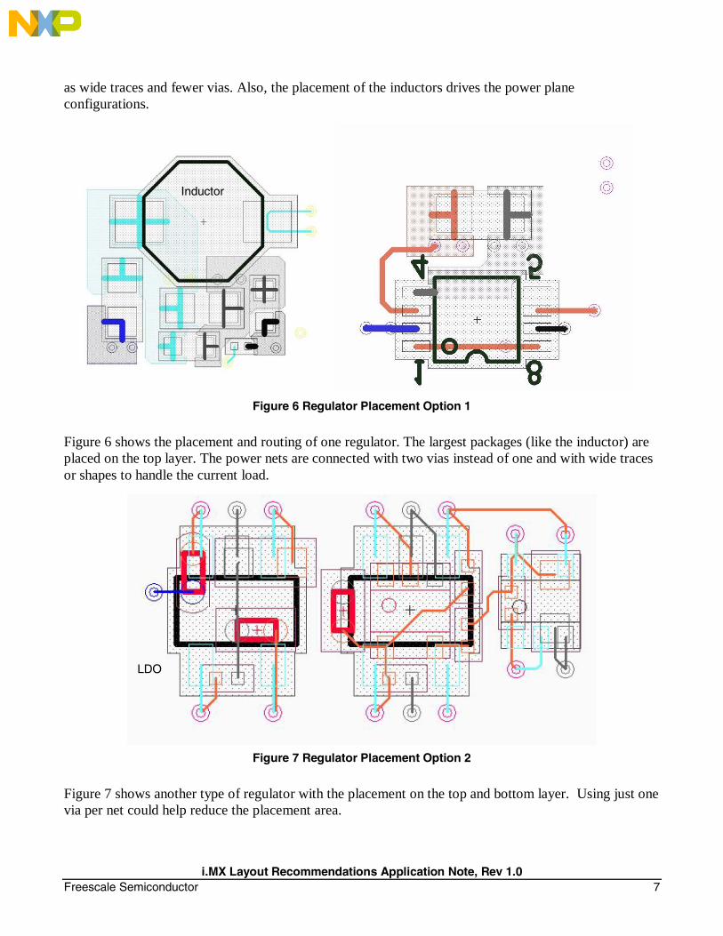
as wide traces and fewer vias. Also, the placement of the inductors drives the power plane configurations.
Figure 6 Regulator Placement Option 1
Figure 6 shows the placement and routing of one regulator. The largest packages (like the inductor) are placed on the top layer. The power nets are connected with two vias instead of one and with wide traces or shapes to handle the current load.
Figure 7 Regulator Placement Option 2
Figure 7 shows another type of regulator with the placement on the top and bottom layer. Using just one via per net could help reduce the placement area.
Inductor
LDO
i.MX Layout Recommendations Application Note, Rev 1.0 8 Freescale Semiconductor
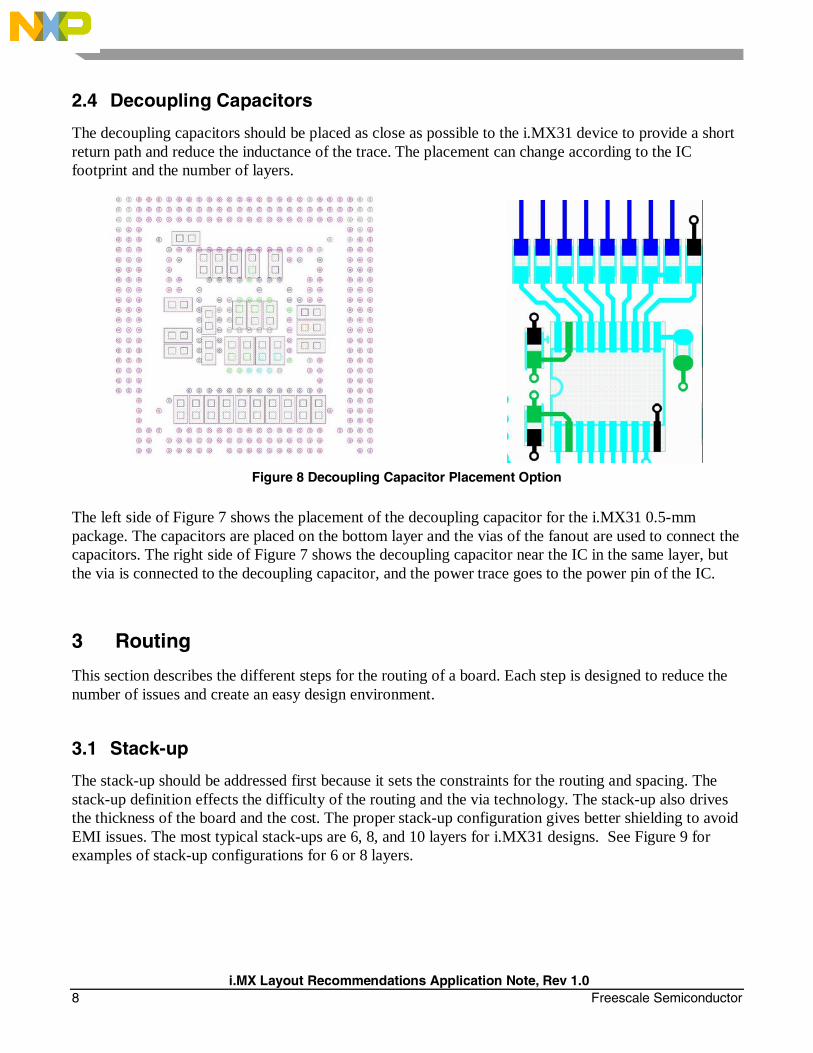
2.4 Decoupling Capacitors
The decoupling capacitors should be placed as close as possible to the i.MX31 device to provide a short return path and reduce the inductance of the trace. The placement can change according to the IC footprint and the number of layers.
Figure 8 Decoupling Capacitor Placement Option
The left side of Figure 7 shows the placement of the decoupling capacitor for the i.MX31 0.5-mm package. The capacitors are placed on the bottom layer and the vias of the fanout are used to connect the capacitors. The right side of Figure 7 shows the decoupling capacitor near the IC in the same layer, but the via is connected to the decoupling capacitor, and the power trace goes to the power pin of the IC.
3 Routing
This section describes the different steps for the routing of a board. Each step is designed to reduce the number of issues and create an easy design environment.
3.1 Stack-up
The stack-up should be addressed first because it sets the constraints for the routing and spacing. The stack-up definition effects the difficulty of the routing and the via technology. The stack-up also drives the thickness of the board and the cost. The proper stack-up configuration gives better shielding to avoid EMI issues. The most typical stack-ups are 6, 8, and 10 layers for i.MX31 designs. See Figure 9 for examples of stack-up configurations for 6 or 8 layers.

i.MX Layout Recommendations Application Note, Rev 1.0 Freescale Semiconductor 9
Signal
Plane
Figure 9 Stack-up Configurations
3.2 Fanout
Freescale recommends completing the fanout of all the components before the routing of the nets to determine the real space and restrictions for the routing. The fanout describes the way in which the vias are placed in order to access the i.MX31 pins. The fanout is determined by the pitch, via configuration, and signals.
The types of fanout are as follows (see Figure 10):
• Place a via-in-pad in each pad
• Place some vias towards the outside of the pin field and others towards the center of the pin field
• Place the vias at a 45° angle to the device edge, which creates two routing channels in the middle of the BGA
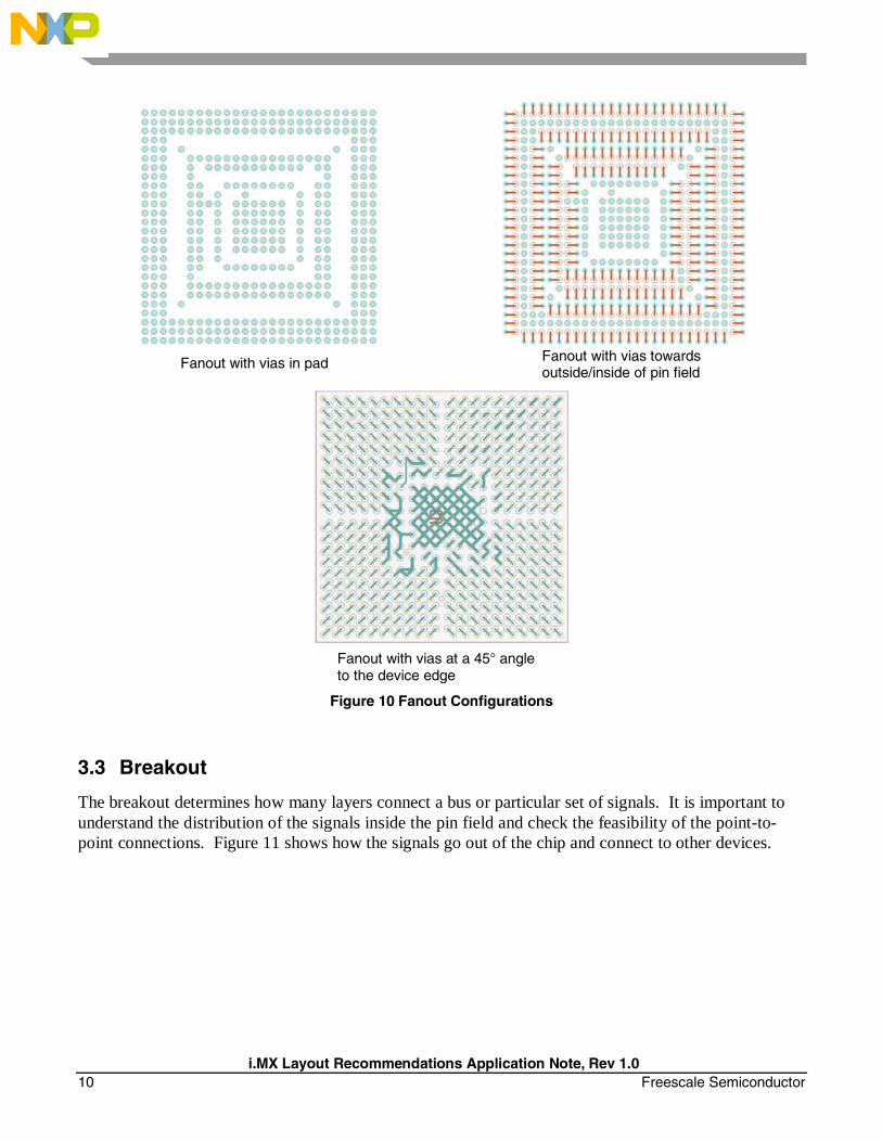
i.MX Layout Recommendations Application Note, Rev 1.0 10 Freescale Semiconductor
Figure 10 Fanout Configurations
3.3 Breakout
The breakout determines how many layers connect a bus or particular set of signals. It is important to understand the distribution of the signals inside the pin field and check the feasibility of the point-to- point connections. Figure 11 shows how the signals go out of the chip and connect to other devices.
Fanout with vias in pad Fanout with vias towards outside/inside of pin field
Fanout with vias at a 45° angle to the device edge

i.MX Layout Recommendations Application Note, Rev 1.0 Freescale Semiconductor 11
Figure 11 Breakout
3.4 Critical Routing
The i.MX31 routing is considered a high-speed layout, but not all signals should be routed with high- speed constraints. The following sections discuss the critical routing issues for i.MX boards.
3.4.1 Differential Pairs
3.4.1.1 DDR Memory Clock
The differential clock of a DDR interface should be routed at 100 Ω differential characteristic impedance. This clock signal should not change layers while routing. After the fanout of the components, the clock should have a point-to-point connection using a single layer. The clock routing should be kept away from other signals as much as possible. See Figure 12 for an example.
Figure 12 DDR Memory Differential Clock Routing
i.MX Layout Recommendations Application Note, Rev 1.0 12 Freescale Semiconductor
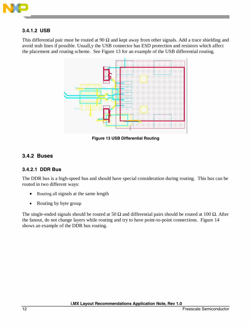
3.4.1.2 USB
This differential pair must be routed at 90 Ω and kept away from other signals. Add a trace shielding and avoid stub lines if possible. Usuall,y the USB connector has ESD protection and resistors which affect the placement and routing scheme. See Figure 13 for an example of the USB differential routing.
Figure 13 USB Differential Routing
3.4.2 Buses
3.4.2.1 DDR Bus
The DDR bus is a high-speed bus and should have special consideration during routing. This bus can be routed in two different ways:
• Routing all signals at the same length
• Routing by byte group
The single-ended signals should be routed at 50 Ω and differential pairs should be routed at 100 Ω. After the fanout, do not change layers while routing and try to have point-to-point connections. Figure 14 shows an example of the DDR bus routing.
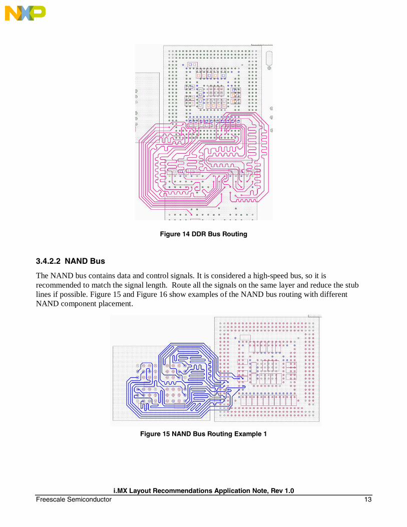
i.MX Layout Recommendations Application Note, Rev 1.0 Freescale Semiconductor 13
Figure 14 DDR Bus Routing
3.4.2.2 NAND Bus
The NAND bus contains data and control signals. It is considered a high-speed bus, so it is recommended to match the signal length. Route all the signals on the same layer and reduce the stub lines if possible. Figure 15 and Figure 16 show examples of the NAND bus routing with different NAND component placement.
Figure 15 NAND Bus Routing Example 1

i.MX Layout Recommendations Application Note, Rev 1.0 14 Freescale Semiconductor
Figure 16 NAND Bus Routing Example 2
3.4.2.3 SD Bus
The data and control signal of the SD bus should be routed with matching lengths and on the same layer.
3.4.2.4 USB Bus
The OTG feature on i.MX31 has a ULPI interface that contains data and control lines. These lines must be connected to the ULPI transceiver and must be treated as high speed signals. To avoid data timing issues, it is recommended to match the length of all the lines; see Figure 17.

i.MX Layout Recommendations Application Note, Rev 1.0 Freescale Semiconductor 15
Figure 17 USB Bus Routing
3.4.2.5 LCD and CSI Bus
The LCD and CSI buses handle data from the camera and LCD modules. It is important to route these signals the same length and keep them away from other signals if possible.
3.4.2.6 SPI and I2C Bus
The SPI and I2C buses communicate with other devices or interfaces. It is recommended to match the length of these signals. When there is more than one device on the bus, route all the signals in a daisy chain as seen in Figure 18.
Figure 18 SPI and I2C Bus Routing
i.MX31
Device 2
Device 1
ULPI

i.MX Layout Recommendations Application Note, Rev 1.0 16 Freescale Semiconductor
3.4.3 Analog and RF
3.4.3.1 Analog
The analog signals, such as the ADC signals, should be routed away from the digital buses and components. If possible, use one layer for analog routing adjacent to the returned path of analog ground.
3.4.3.2 Bluetooth®
The routing of the Bluetooth signals and components should follow the layout recommendations from the Bluetooth IC manufacturer using 50-Ω traces for the antenna signals. Establish a specific area for the placement of Bluetooth components and avoid routing other signals behind that area, as seen in Figure 19.
Figure 19 Bluetooth Routing
WiFi Area
Bluetooth Area

i.MX Layout Recommendations Application Note, Rev 1.0 Freescale Semiconductor 17
3.5 Power Planes
The power planes should be solid and include enough copper to handle the return current path. Plan the vias that connect to the power plane carefully and avoid having necks on the plane. The air gap between the planes should be 15 mils. The minimum spacing is defined by manufacturing constraints. Figure 20 shows an example of power planes.
Figure 20 Power Planes
Use more than one via when connecting top or bottom planes to an inner layer. Also, add GND vias near the power vias if possible. Figure 21shows an example of how the power planes from top are connected to the inner or bottom layers. For this example, the connection is made with four vias, but the number of vias depends on the board spacing. This type of configuration can reduce the complexity of the power planes and avoid adding more power plane layers.

i.MX Layout Recommendations Application Note, Rev 1.0 18 Freescale Semiconductor
Figure 21. Power Planes

i.MX Layout Recommendations Application Note, Rev 1.0 Freescale Semiconductor 19
THIS PAGE INTENTIONALLY LEFT BLANK

Document Number: AN3951 Rev.1.0 09/2008
How to Reach Us:
Home Page: www.freescale.com
Web Support: http://www.freescale.com/support
USA/Europe or Locations Not Listed: Freescale Semiconductor Technical Information Center, EL516 2100 East Elliot Road Tempe, Arizona 85284 +1-800-521-6274 or +1-480-768-2130 www.freescale.com/support
Europe, Middle East, and Africa: Freescale Halbleiter Deutschland GmbH Technical Information Center Schatzbogen 7 81829 Muenchen, Germany +44 1296 380 456 (English) +46 8 52200080 (English) +49 89 92103 559 (German) +33 1 69 35 48 48 (French) www.freescale.com/support
Japan: Freescale Semiconductor Japan Ltd. Headquarters ARCO Tower 15F 1-8-1, Shimo-Meguro, Meguro-ku, Tokyo 153-0064, Japan 0120 191014 or +81 3 5437 9125 [email protected]
Asia/Pacific: Freescale Semiconductor China Ltd. Exchange Building 23F No. 118 Jianguo Road Chaoyang District Beijing 100022 China +86 010 5879 8000 [email protected]
For Literature Requests Only: Freescale Semiconductor Literature Distribution Center P.O. Box 5405 Denver, Colorado 80217 1-800-441-2447 or 303-675-2140 Fax: 303-675-2150 [email protected]
Information in this document is provided solely to enable system and software implementers to use Freescale Semiconductor products. There are no express or implied copyright licenses granted hereunder to design or fabricate any integrated circuits or integrated circuits based on the information in this document.
Freescale Semiconductor reserves the right to make changes without further notice to any products herein. Freescale Semiconductor makes no warranty, representation or guarantee regarding the suitability of its products for any particular purpose, nor does Freescale Semiconductor assume any liability arising out of the application or use of any product or circuit, and specifically disclaims any and all liability, including without limitation consequential or incidental damages. “Typical” parameters that may be provided in Freescale Semiconductor data sheets and/or specifications can and do vary in different applications and actual performance may vary over time. All operating parameters, including “Typicals”, must be validated for each customer application by customer’s technical experts. Freescale Semiconductor does not convey any license under its patent rights nor the rights of others. Freescale Semiconductor products are not designed, intended, or authorized for use as components in systems intended for surgical implant into the body, or other applications intended to support or sustain life, or for any other application in which the failure of the Freescale Semiconductor product could create a situation where personal injury or death may occur. Should Buyer purchase or use Freescale Semiconductor products for any such unintended or unauthorized application, Buyer shall indemnify and hold Freescale Semiconductor and its officers, employees, subsidiaries, affiliates, and distributors harmless against all claims, costs, damages, and expenses, and reasonable attorney fees arising out of, directly or indirectly, any claim of personal injury or death associated with such unintended or unauthorized use, even if such claim alleges that Freescale Semiconductor was negligent regarding the design or manufacture of the part.
Freescale and the Freescale logo are trademarks or registered trademarks of Freescale Semiconductor, Inc. in the U.S. and other countries. All other product or service names are the property of their respective owners. Bluetooth is a registered trademark of the Bluetooth SIG, Inc., and is used under license.
© Freescale Semiconductor, Inc. 2009. All rights reserved.