
Impurities and Defects in Photovoltaic Si Devices: A … and Defects in Photovoltaic Si Devices: A...
16
Impurities and Defects in Photovoltaic Si Devices: A Review Preprint November 1999 • NREL/CP-520-27524 B. Sopori To Be Presented at the 10 th International Workshop on the Physics of Semiconductor Devices Delhi, India December 13, 1999 National Renewable Energy Laboratory 1617 Cole Boulevard Golden, Colorado 80401-3393 NREL is a U.S. Department of Energy Laboratory Operated by Midwest Research Institute • Battelle • Bechtel Contract No. DE-AC36-98-GO10337
Transcript of Impurities and Defects in Photovoltaic Si Devices: A … and Defects in Photovoltaic Si Devices: A...

Impurities and Defects inPhotovoltaic Si Devices:A Review
Preprint
November 1999 • NREL/CP-520-27524
B. Sopori
To Be Presented at the 10th International Workshopon the Physics of Semiconductor DevicesDelhi, IndiaDecember 13, 1999
National Renewable Energy Laboratory1617 Cole BoulevardGolden, Colorado 80401-3393NREL is a U.S. Department of Energy LaboratoryOperated by Midwest Research Institute •••• Battelle •••• Bechtel
Contract No. DE-AC36-98-GO10337

NOTICEThe submitted manuscript has been offered by an employee of the Midwest Research Institute (MRI), acontractor of the US Government under Contract No. DE-AC36-99GO10337. Accordingly, the USGovernment and MRI retain a nonexclusive royalty-free license to publish or reproduce the publishedform of this contribution, or allow others to do so, for US Government purposes.
This report was prepared as an account of work sponsored by an agency of the United Statesgovernment. Neither the United States government nor any agency thereof, nor any of their employees,makes any warranty, express or implied, or assumes any legal liability or responsibility for the accuracy,completeness, or usefulness of any information, apparatus, product, or process disclosed, or representsthat its use would not infringe privately owned rights. Reference herein to any specific commercialproduct, process, or service by trade name, trademark, manufacturer, or otherwise does not necessarilyconstitute or imply its endorsement, recommendation, or favoring by the United States government or anyagency thereof. The views and opinions of authors expressed herein do not necessarily state or reflectthose of the United States government or any agency thereof.
Available electronically at http://www.doe.gov/bridge
Available for a processing fee to U.S. Department of Energyand its contractors, in paper, from:
U.S. Department of EnergyOffice of Scientific and Technical InformationP.O. Box 62Oak Ridge, TN 37831-0062phone: 865.576.8401fax: 865.576.5728email: [email protected]
Available for sale to the public, in paper, from:U.S. Department of CommerceNational Technical Information Service5285 Port Royal RoadSpringfield, VA 22161phone: 800.553.6847fax: 703.605.6900email: [email protected] ordering: http://www.ntis.gov/ordering.htm
Printed on paper containing at least 50% wastepaper, including 20% postconsumer waste

1
Impurities and Defects in Photovoltaic Si Devices: A Review
Bhushan SoporiNational Renewable Energy laboratory
1617 Cole BoulevardGolden, Co 80401
ABSTRACT
The performance of commercial photovoltaic Si devices is strongly controlled by the impuritiesand defects present in the substrates. A well-designed solar cell processing sequence canmitigate their effects to yield high efficiency devices. Such a process-design requires acomprehensive knowledge of the properties of defects, impurities, and impurity-defectinteractions that can occur during device processing. This paper reviews the recentunderstanding of the impurity and defect issues in Si-photovoltaics.
INTRODUCTION
The photovoltaic silicon (PV-Si) industry uses both single- and multi-crystalline (mc) wafers thatare grown by techniques specially developed to produce low-cost material. Typically, the singlecrystal ingots are grown by a Czochralski (CZ)-type process, and mc-Si is either cast or in theribbon form. Because the substrate cost must be kept low, the PV industry employs a host ofcost-cutting measures that include low-quality poly feedstock, a lower degree of cleanliness andcontrol in the crystal growth process, and a high crystal-growth rate. These cost-cutting measurescompromise the crystallinity as well as the chemical purity of the material. Concomitantly, thePV-Si has high concentrations of impurities and defects [1].
A major goal in solar cell fabrication is to be able to design process schedules that can minimizethe deleterious effects of the impurities, defects, and (or) passivate them [2-4]. Indeed, it ispossible to design cell processing steps that can accomplish a significant reduction in thedissolved impurity concentrations and produce favorable impurity/defect interactions as abyproduct. Such processes have led to commercial Si solar cells with efficiencies of 14-15%.However, further improvements in the device performance requires using new concepts that canmitigate the deleterious effects resulting from impurity-defect interactions during crystal growthand device fabrication.
This paper reviews the basic behavior of impurities and defects in Si. We show that impurity-defect interactions play an important role in determining the performance of silicon PV devices,and it is necessary to know such interactions to design processes that can mitigate theirdetrimental effects on the device performance.

2
IMPURITIES AND DEFECTS IN PV-Si
Si-PV manufacturers use low-grade feedstock consisting of pot-scrap, off-spec, and remelt—much of this material is the reject from the microelectronic industry. The impurities present inthe feedstock are carried into the melt and into the grown crystal dictated by the segregationcoefficients. Hence, in general, the PV starting material has a high impurity content. Typicallythese substrates contain C and/or O in near-saturation levels, transition metals in the range of1012-1014 cm-3, and a host of other impurities such as Ti and Va.
Because of their high concentrations, in many cases impurities can precipitate at preferred sitessuch as extended defects, grain boundaries, and defect clusters. The chemical structure of suchprecipitates can be quite complex. For example, micro-X-ray analyses have shown that someprecipitates are predominantly metallic but have significant amounts of oxygen and or carbonassociated with them. This may indicate that metal precipitates are silicides, carbides, andoxides. On the other hand, this may mean that metal precipitation is a secondary process thattakes place in the proximity of pre-existing oxygen/carbon precipitates. Such a phenomenonmay occur as a local stress relaxation mechanism.
The single-crystal CZ ingots for PV are pulled at growth rates that can be many times faster thanthat of the conventional growth for microelectronics. These fast cooling rates are accompaniedby excessive thermal stresses that lead to generation of defects. Consequently, the single crystalmaterial is expected to have high concentrations of quenched-in, non-equilibrium, point defects.In some cases, a portion of the ingot may acquire a high density of crystal defects (primarilydislocations) and even lose the crystallinity and become multicrystalline. The mc-Si substratestypically consist of very large grains with a small grain boundary area producing only a smalleffect on the device performance. The dominant intragrain defect is dislocation. High-qualitymc-Si substrates have a tendency to form clusters of defects. Figure 1 is a map of a typical, 4.25-in x 4.25-in, commercial, multicrystalline PV-Si wafer. The wafer has an average defect densityof about 105cm-2; however, as seen in the figure, there are localized clusters of defects where thedefect density can exceed 107cm-2. Our previous work has shown that such defects consist ofnetworks of dislocations, stacking faults and grain boundaries. Detailed analyses have shownthat such defect clusters are sites of impurity precipitates. Figure 2 shows a TEM photograph ofprecipitates at a defect cluster. It is rather interesting that impurity precipitation occurs at defectclusters rather than at grain boundaries and other isolated defects [1].
Wafers of mc-Si exhibit a preponderance of twins. The most commonly observed twins arecoherent twin-lamelli that have a (111) twinning plane. A high-quality wafer may have 20–30%of the area covered by such twins. These regions are generally free of dislocations and constitutethe best quality material in a wafer. In addition to the coherent twins, the wafers have higherorder twin boundaries, which are often decorated with dislocations.

3
RECOMBINATION CAUSED BY IMPURITIES AND DEFECTS
Impurities and defects introduce energy levels in the bandgap with a concomitant increase in theminority-carrier recombination. The impurities of most interest in PV-Si are the transitionmetals (TM), particularly Fe, Cr, and Ni. In the dissolved state, these impurities are highlymobile with diffusivities close to 10-6 cm2 s-1, and they produce deep levels. Typically, the totalconcentration of the TM is quite high, near 1014cm-3. It is fruitful to consider some details oftheir recombination properties in Si. We can use Fe as an example; other metals have asomewhat similar behavior. In the past thirty years, Fe in Si has been studied extensively, both
→→→→
Figure 1. Dislocation density map of a commercial 4.25-in x 4.25-in mc-Siwafer. The numbers in the legend indicate dislocation density in cm-2. Theinset on the left shows a magnified view of the region indicated by the arrows.
500 A
↓
Figure 2. A TEMphotograph showingimpurity precipitationat a defect cluster site.µ−X-ray analysesshows that theprecipitates have manyelemental impurities.

4
experimentally and theoretically [5,6]. Iron exists in Si in two forms: as interstitial and as acomplex with other defects. At room temperature, the interstitial iron (Fei) introduces a donorlevel at ET ≈ EV+(0.375±0.015) eV. The hole capture cross-section of interstitial iron can bewritten as (in cm-2):
where kB stands for the Boltzman constant, and T is the temperature. The electron capture cross-section of Fe at room temperature was measured as σn= 4×10-14 cm-2. Because of near-mid gapenergy and a large capture cross section, it is expected that Fe will produce high recombinationor low minority-carrier lifetime.
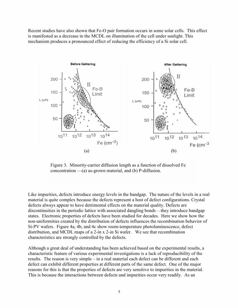
The interstitial iron in p-Si is positively charged at room temperature and at slightly elevatedtemperatures. As a result, it tends to form pairs with negatively charged defects, such as shallowacceptors. More than 30 complexes can be formed between iron and other defects, and about 20deep levels are associated with these complexes. The positions of these energy levels vary fromabout Ev+0.07 eV to Ec-(0.26±0.03) eV. They could be either donor levels or acceptor levels.The hole capture cross section ranges from 3.9x10⁻¹⁶ to 2x10-13 cm-2, while the electron capturecross section can change from 1.5x10⁻¹⁶ to 4x10-13cm-2. Of particular interest is the ability of Feto form complexes with two major impurities in Si-B and O. The B-Fe forms a donor level atEv+0.1 eV (σn= 4×10-13 cm-2 at the room temperature) and an acceptor level at Ec-0.29 eV. Therecombination rate caused by the Fe-B pair is lower than that of interstitial Fe at low injectionlevels. The formation of Fe-B is an important effect that has an implication on solar celltechnology. Fe-B recombination has a more pronounced effect in lower resistivity P-type Si. Atlower temperatures, nearly all Fe present in a Si wafer occurs as Fe-B. In a B-doped PV-Siwafer containing Fe, the recombination can be further increased by the presence of defects.Figure 3a shows the minority carrier diffusion length (MCDL) as a function of Fe concentrationin a PV-Si wafer. The solid line is the calculated curve for Fe-B limited recombination, whilethe crosses indicate experimental data measured by an SPV technique. It is clear that the MCDLis lower than the Fe-B limit, and one may envision two groups of MCDL values identified bynumerals I and II that may correspond to two types of defects. Figure 3b shows themeasurements on the same wafer after a P-diffusion for impurity gettering. This figure showsthat defects associated with group II were gettered, leading to an increase in the MCDL, whilethat of group I remained mainly unaltered. A discussion of this feature is given later in thispaper.
It should be pointed out that Fe-B complexes dissociate at temperatures of about 200°C or byillumination of high intensity light (typically about a few W/cm2). A dissociation of Fe-B resultsin an increase in the recombination and a decrease in τ. It has also been known for a while thatthe values τ in low-resistivity, B-doped substrates are much lower than one can expect on thebasis of impurity scattering by B concentration alone. Recent studies have shown that Fe-B pairformation is responsible for a rapid decrease in the resistivity (in B-doped material). It isimportant to recognize that in a solar cell many impurities are gettered during the cell fabrication.Thus, the behavior of many impurities is quite dynamic in solar cell material.
)005.0045.0exp(10)5.09.3()( 16
TkeVFe
Bip
±−××±= −σ
5
Recent studies have also shown that Fe-O pair formation occurs in some solar cells. This effectis manifested as a decrease in the MCDL on illumination of the cell under sunlight. Thismechanism produces a pronounced effect of reducing the efficiency of a Si solar cell.
Like impurities, defects introduce energy levels in the bandgap. The nature of the levels in a realmaterial is quite complex because the defects represent a host of defect configurations. Crystaldefects always appear to have detrimental effects on the material quality. Defects arediscontinuities in the periodic lattice with associated dangling bonds —they introduce bandgapstates. Electronic properties of defects have been studied for decades. Here we show how thenon-uniformities created by the distribution of defects influences the recombination behavior ofSi-PV wafers. Figure 4a, 4b, and 4c show room-temperature photoluminescence, defectdistribution, and MCDL maps of a 2-in x 2-in Si wafer. We see that recombinationcharacteristics are strongly controlled by the defects.
Although a great deal of understanding has been achieved based on the experimental results, acharacteristic feature of various experimental investigations is a lack of reproducibility of theresults. The reason is very simple – in a real material each defect can be different and eachdefect can exhibit different properties at different parts of the same defect. One of the majorreasons for this is that the properties of defects are very sensitive to impurities in the material.This is because the interactions between defects and impurities occur very readily. As an
Figure 3. Minority-carrier diffusion length as a function of dissolved Feconcentration —(a) as-grown material, and (b) P-diffusion.
(a) (b)

6
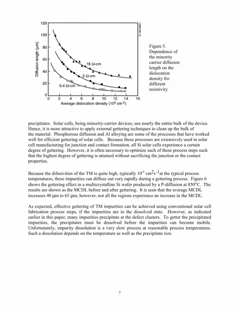
example, Figure 5 shows the MCDL of Si as a function of dislocation density for differentresistivity materials. The effect of dislocations is strongly dependent on the resistivity of thesubstrate.
REMOVAL OF IMPURITIES FROM Si
It is well known that the performance of solar cells would be quite poor if the device had as highconcentrations of impurities as in the as-grown PV-Si. Fortunately, some of the impurities areremoved during the device processing. This mechanism, called gettering, has been used inmicroelectronic devices to trap impurities away from the active region of the device by oxygen
(a)0 105 106 107
Figure 4. Correlation between (a) PL,(b) defect density, and (c) MCDLmaps of a 2-in x 2-in mc-Si sample.
(c)
(b
7
precipitates. Solar cells, being minority-carrier devices, use nearly the entire bulk of the device.Hence, it is more attractive to apply external gettering techniques to clean up the bulk ofthe material. Phosphorous diffusion and Al alloying are some of the processes that have workedwell for efficient gettering of solar cells. Because these processes are extensively used in solarcell manufacturing for junction and contact formation, all Si solar cells experience a certaindegree of gettering. However, it is often necessary to optimize each of these process steps suchthat the highest degree of gettering is attained without sacrificing the junction or the contactproperties.
Because the difusivities of the TM is quite high, typically 10-6 cm2s-1at the typical processtemperatures, these impurities can diffuse out very rapidly during a gettering process. Figure 6shows the gettering effect in a multicrystalline Si wafer produced by a P-diffusion at 850°C. Theresults are shown as the MCDL before and after gettering. It is seen that the average MCDLincreases 40 µm to 65 µm; however, not all the regions experience an increase in the MCDL.
As expected, effective gettering of TM impurities can be achieved using conventional solar cellfabrication process steps, if the impurities are in the dissolved state. However, as indicatedearlier in this paper, many impurities precipitate at the defect clusters. To getter the precipitatedimpurities, the precipitates must be dissolved before the impurities can become mobile.Unfortunately, impurity dissolution is a very slow process at reasonable process temperatures.Such a dissolution depends on the temperature as well as the precipitate size.
Figure 5.Dependence ofthe minoritycarrier diffusionlength on thedislocationdensity frodifferentresistivity

8
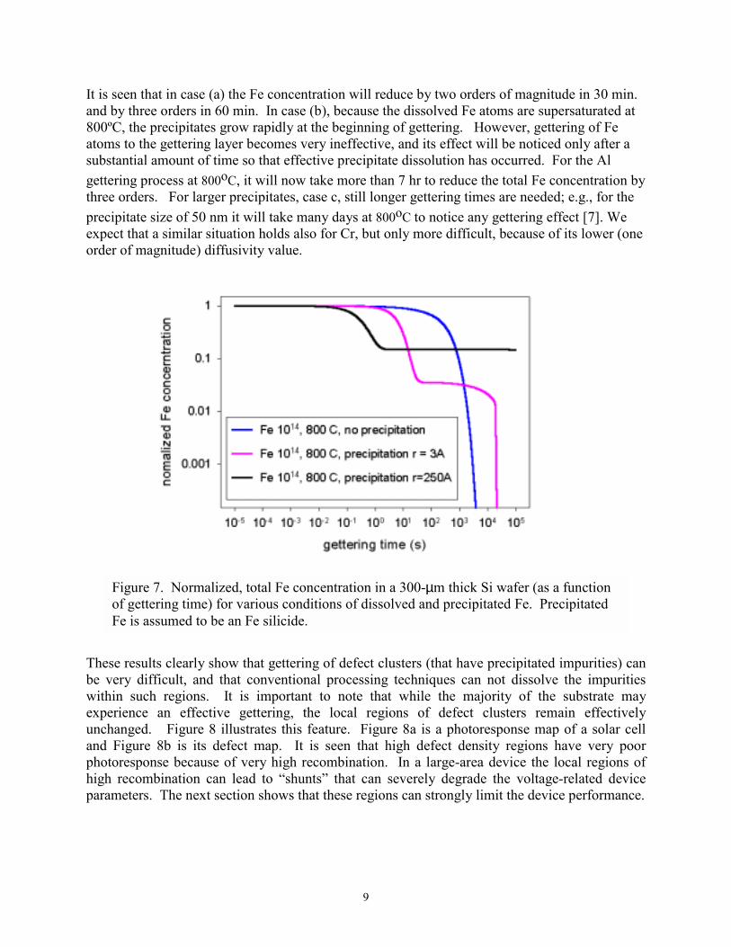
Again, we can use Fe as the “test” impurity to study the gettering behavior resulting from an Alalloying process. Typically Al alloying is done at 800ºC, using 1 µm of Al. We consider a300-µm-thick wafer having a dissolved Fe concentration of 1014 cm-3, and examine changes inthe total Fe, integrated within the thickness of the wafer, as a function of gettering time (on anormalized scale). Figure 7 shows these results for three cases — (a) Fe dissolved to aconcentration of 1014 cm-3 without any precipitates, (b) additional precipitates, 6 nm in diameteras a silicide, concentration of 1011 cm-3 (which adds about 5x1011 cm-3 Fe atoms inprecipitated form , and (c) precipitates 50 nm in size.
Figure 6. Comparison of the minority carrier diffusion length before (a) andafter P gettering (b).Gettering: 850°C, 15 min
(b)(a)
9
It is seen that in case (a) the Fe concentration will reduce by two orders of magnitude in 30 min.and by three orders in 60 min. In case (b), because the dissolved Fe atoms are supersaturated at800ºC, the precipitates grow rapidly at the beginning of gettering. However, gettering of Featoms to the gettering layer becomes very ineffective, and its effect will be noticed only after asubstantial amount of time so that effective precipitate dissolution has occurred. For the Algettering process at 800oC, it will now take more than 7 hr to reduce the total Fe concentration bythree orders. For larger precipitates, case c, still longer gettering times are needed; e.g., for theprecipitate size of 50 nm it will take many days at 800oC to notice any gettering effect [7]. Weexpect that a similar situation holds also for Cr, but only more difficult, because of its lower (oneorder of magnitude) diffusivity value.
These results clearly show that gettering of defect clusters (that have precipitated impurities) canbe very difficult, and that conventional processing techniques can not dissolve the impuritieswithin such regions. It is important to note that while the majority of the substrate mayexperience an effective gettering, the local regions of defect clusters remain effectivelyunchanged. Figure 8 illustrates this feature. Figure 8a is a photoresponse map of a solar celland Figure 8b is its defect map. It is seen that high defect density regions have very poorphotoresponse because of very high recombination. In a large-area device the local regions ofhigh recombination can lead to “shunts” that can severely degrade the voltage-related deviceparameters. The next section shows that these regions can strongly limit the device performance.
Figure 7. Normalized, total Fe concentration in a 300-µm thick Si wafer (as a functionof gettering time) for various conditions of dissolved and precipitated Fe. PrecipitatedFe is assumed to be an Fe silicide.

10
THE INFLUENCE OF DEFECTS AND IMPURITIES ON THE DEVICE PERFORMANCE
As discussed above, presence of impurities and defects makes a solar cell a non-uniform device.In the previous section, we have already seen that defects and impurities can lower the MCDL inthe as-grown substrate. Predicting the effect of impurities and defects on the device performanceis, however, quite difficult [8]. A quantitative investigation of the effect of defects on the cellperformance can be performed using a phenomenological approach that involves the followingsteps:
1. Determine the characteristics of the cell with no defects2. Determine the characteristics of the cell corresponding to the defect cluster region, and3. Combine the above two to form a distributed device having a given distribution of defect
clusters.
Item 1 is straightforward and can be expressed in a standard form as:
Jdark(V) = J01.exp.{ (-eV/kT) - 1} + J02. { exp. (-eV/2kT) - 1}
The saturation currents J01.and J02 can be written as:J = Jph - Jdark(V), where Jph and Jdark(V) are the photogenerated and the dark current densities,respectively.
0 105 106 1074000 5000 6000 7000 80003000
Figure 8. (a) A photoresponse map of a solar cell taken with a long wavelengthexcitation showing the bulk response of the device. The defect map of the deviceis shown in (b). The scales are in counts and defects cm-2, respectively.

11
A similar formalism can be applied to the local, defected region of a solar cell [3]. Becausedefects can propagate in different regions of the device (see Figure 9), one must consider theirinfluence on the base as well as the junction regions. We have shown that the defected regioncan also be represented by equations similar to 1 and 2 above. However, in this case the valuesof various parameters will be different. We have developed a computer model for an N/Pjunction device that calculates these parameters and uses a distributed network model to combinevarious regions of the device.
The device is divided into an array of diodes, each diode is small enough to assume a uniformdistribution of defects. Each node in the matrix depicts a local cell, connected to other cells by aresistor representing the series resistance. The series resistance arises from a number of sources thatinclude the sheet resistivity of the junction in an N/P device.
We consider an example of a cell in which 20% of the device area is covered by heavily defectedregions, and 80% of the area is defect-free. The parameters for the defect-free region are: Jph= 0.035A/cm2, J01= 3.6 x 10⁻⁹ A/cm2 , J02= 4.5 x 10⁻¹³ A/cm2
From the experimental data, the parameters for the “defected” cell are: Jph= 0.0245 A/cm2 , J01= 3.6 x 10⁻⁸ A/cm2 , J02= 4.5x 10⁻¹¹ A/cm2
Figure 10 shows the calculated I-V characteristics of these two cells. Their cell parameters are:{Voc= 650 mV, Jsc= 34.45 mA/cm2, FF= 81.01, and the efficiency=18.4}for defect-free and{Voc= 620mV, Jsc=32.7 mA/cm2, FF= 75.76, Eff = 16.7} for defected cells, respectively. It isseen that all the parameters of the “defected” cell are lower than for the “defect-free” cell.However, the major reduction is in the Voc and the FF. It should be pointed out that in an“undefected” cell , a reduction of 30 mV would be accompanied by a large reduction in Jsc inaccordance with the cell equation; shunting produces a disproportionate reduction in the voltage.
Figure 9. Aschematicillustratingrecombination dueto defects in a PNjunction device
12
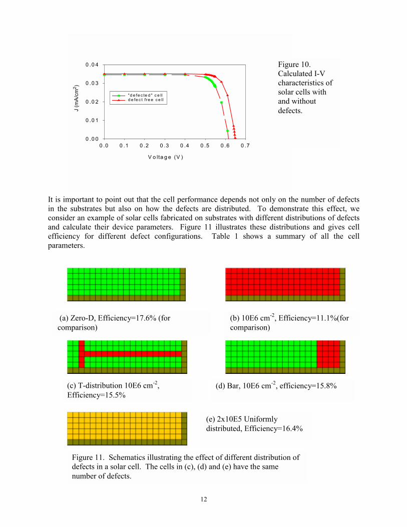
It is important to point out that the cell performance depends not only on the number of defectsin the substrates but also on how the defects are distributed. To demonstrate this effect, weconsider an example of solar cells fabricated on substrates with different distributions of defectsand calculate their device parameters. Figure 11 illustrates these distributions and gives cellefficiency for different defect configurations. Table 1 shows a summary of all the cellparameters.
V o lta g e (V )
0 .0 0 .1 0 .2 0 .3 0 .4 0 .5 0 .6 0 .7
J (m
A/cm
2 )
0 .0 0
0 .0 1
0 .0 2
0 .0 3
0 .0 4
"d e fe c te d " c e lld e fe c t fre e c e ll
Figure 10.Calculated I-Vcharacteristics ofsolar cells withand withoutdefects.
(a) Zero-D, Efficiency=17.6% (forcomparison)
(c) T-distribution 10E6 cm-2,Efficiency=15.5%
(b) 10E6 cm-2, Efficiency=11.1%(forcomparison)
(e) 2x10E5 Uniformlydistributed, Efficiency=16.4%
(d) Bar, 10E6 cm-2, efficiency=15.8%
Figure 11. Schematics illustrating the effect of different distribution ofdefects in a solar cell. The cells in (c), (d) and (e) have the samenumber of defects.

13
Table 1. Summary of the solar cell parameters for different distribution of defects
Cellconfiguration
Efficiency(%)
Voc (mV) Jsc (mA/cm2) FF (%)
No defects 17.6 650 34.9 77.620% bar 15.8 615 33.2 77.420% T 15.5 615 33.2 75.9
Uniform 16.4 650 32.5 77.6All defects 11.1 565 26.2 75
CONCLUSIONS
We have reviewed some basic properties of impurities and defects in PV-Si devices. Dissolvedimpurities, particularly TM, can be easily gettered during cell fabrication. Fe is used as anexample to show various mechanisms that can influence the carrier recombination behavior in Si.The defect clusters are sites for impurity precipitation, particularly for the metallic impurities.The chemical nature and the precipitate size can play an important role in whether it can begettered from the device. Thus, it is important to know the chemical composition of theprecipitates. Examples are given to show how defects and impurities can influence the solar cellperformance. Modeling results are presented to show that both the number and the distributionof defects play an important role in the performance of a solar cell.
ACKNOWLEDGEMENT
The author would like to thank Wei Chen for his help in preparing this manuscript. This workwas supported by the US Department of Energy under Contract No.DE-AC36-99GO10337.
REFERENCES
[1] Bhushan Sopori, Procd. ICDS-19, Trans Tech Pub., Edited by Gordon Davies and MariaHelena Nazare, 527 (1997).
[2] B. L. Sopori, L. Jastrzebski, T. Y. Tan, and S. Narayanan, Procd. 12th PVSEC, 1003(1994).[3] B. L. Sopori, W. Chen, K. Nemire, J. Gee, S. Ostapenko, Procd. 2nd World Conference on
Photovoltaic Solar Energy Conversion, Vienna, 152 (1998).[4] B. L. Sopori et.al , Solar Energy Materials and Solar Cells, 41/42, 159 (1996).[5] A. A. Istratov, H. Hieslmair, and E. R. Weber, Appl. Phys. A69, 13-44 (1999).[6] Proceedings of the 9th Workshop on Crystalline Silicon Solar Cell Materials and Processes, NREL/BK-520-26941, Edited by B. L. Sopori.[7] B. L. Sopori, W. Chen, T. Y. Tan, and P. Plekhanov, NCPV Photovoltaics Program Review, AIP Conference Proceedings, 462, Editors, M. Al-Jassim, J. Thornton, and J. Gee, 341 (1998).[8] J. G. Fossum and F. A. Lindholm., IEEE Trans. ED-27, 692(1980).

REPORT DOCUMENTATION PAGE Form ApprovedOMB NO. 0704-0188
Public reporting burden for this collection of information is estimated to average 1 hour per response, including the time for reviewing instructions, searching existingdata sources, gathering and maintaining the data needed, and completing and reviewing the collection of information. Send comments regarding this burdenestimate or any other aspect of this collection of information, including suggestions for reducing this burden, to Washington Headquarters Services, Directorate forInformation Operations and Reports, 1215 Jefferson Davis Highway, Suite 1204, Arlington, VA 22202-4302, and to the Office of Management and Budget, PaperworkReduction Project (0704-0188), Washington, DC 20503.
1. AGENCY USE ONLY (Leave blank) 2. REPORT DATENovember 1999
3. REPORT TYPE AND DATES COVEREDconference paper
4. TITLE AND SUBTITLEImpurities and Defects in Photovoltaic Si Devices: A Review6. AUTHOR(S)B. Sopori
5. FUNDING NUMBERS
CTA: PV003101
7. PERFORMING ORGANIZATION NAME(S) AND ADDRESS(ES) 8. PERFORMING ORGANIZATIONREPORT NUMBER
9. SPONSORING/MONITORING AGENCY NAME(S) AND ADDRESS(ES)National Renewable Energy Laboratory1617 Cole Blvd.Golden, CO 80401-3393
10. SPONSORING/MONITORINGAGENCY REPORT NUMBER
CP-520-27524
11. SUPPLEMENTARY NOTES
12a. DISTRIBUTION/AVAILABILITY STATEMENTNational Technical Information ServiceU.S. Department of Commerce5285 Port Royal RoadSpringfield, VA 22161
12b. DISTRIBUTION CODE
13. ABSTRACT (Maximum 200 words)The performance of commercial photovoltaic Si devices is strongly controlled by the impurities and defects present in the substrates. Awell-designed solar cell processing sequence can mitigate their effects to yield high efficiency devices. Such a process-design requires acomprehensive knowledge of the properties of defects, impurities, and impurity-defect interactions that can occur during deviceprocessing. This paper reviews the recent understanding of the impurity and defect issues in Si-photovoltaics.
15. NUMBER OF PAGES 14. SUBJECT TERMSphotovoltaics ; silicon ; solar cells ; impurities and defects
16. PRICE CODE
17. SECURITY CLASSIFICATIONOF REPORTUnclassified
18. SECURITYCLASSIFICATIONOF THIS PAGEUnclassified
19. SECURITY CLASSIFICATIONOF ABSTRACTUnclassified
20. LIMITATION OF ABSTRACT
UL
NSN 7540-01-280-5500 Standard Form 298 (Rev. 2-89)Prescribed by ANSI Std. Z39-18
298-102


![Document5 - Universidade de Aveiro · undoped GaN is commonly attributed to these point defects [10] [11]. Also, impurities as O [12] and C [1] as well as complex defects like VGa-O](https://static.fdocuments.net/doc/165x107/5ffcfe650f3dd929b9506a95/document5-universidade-de-aveiro-undoped-gan-is-commonly-attributed-to-these-point.jpg)