Improving Loading and Unloading Transient Response of a ...pemic/publications/conf041.pdf ·...
8
Improving Loading and Unloading Transient Response of a Voltage Regulator Module Using a Load-Side Auxiliary Gyrator Circuit Or Kirshenboim, Alon Cervera, and Mor Mordechai Peretz The Center for Power Electronics and Mixed-Signal IC, Department of Electrical and Computer Engineering Ben-Gurion University of the Negev, P.O. Box 653, Beer-Sheva, 8410501 Israel [email protected], [email protected], [email protected] http://www.ee.bgu.ac.il/~pel Abstract— This paper introduces a new voltage regulator module (VRM) that hybrids a highly efficient switched-inductor converter as the main unit with a load- side switched-capacitor based converter to assist during load transient events. The resulting hybrid-VRM exhibits improved dynamic performance for both loading and unloading transient events, while maintaining a compact design with reduced stress of the components. The hybrid controller that has been developed allows operation based on output voltage measurement alone, further reducing the circuit complexity. The operation of the VRM is verified on a 30W, 12V-to-1.5V prototype, demonstrating a near-ideal transient recovery. Index Terms— Voltage regulation module, switch-mode power supply, improved transient-response, optimal control, digital control, auxiliary circuit I. INTRODUCTION In recent years there has been a sharp rise in interest and demand for more compact, light, energy efficient and economical voltage regulation solutions. In particular, tighter output voltage regulation, faster response times and lower volume are of major concern in the design of present-day voltage-regulator modules (VRM). For processing power from fractions of a watt to several tens of watts with fast transient performance, multi-stage interleaved converters combined with analog controllers have been predominantly used [1]-[5]. There, fast response is usually achieved by designing a wide bandwidth control loop. The advancement in hardware-efficient digital controllers [6]-[9] enabled the implementation of advanced nonlinear control methods that improve the dynamic performance and, as a consequence, drastically reduce the size of the output capacitor. Among them, time-optimal control (TOC) [10]-[16] and minimum-deviation [17] controllers have demonstrated transient response with virtually the smallest possible voltage deviation, restricted only by the inductor’s slew-rate. In VRM applications, this limitation has a major effect on the output voltage deviation for the case of an unloading transient event, primarily due to the high input-to-output conversion ratio. Another weakness of the classical time-optimal approach is the relatively higher current stress, beyond the steady-state value, that is required to restore the lost charge of the output capacitor during the recovery time [16],[18]. As a result, the overall power processing efficiency is impacted from consecutive transients, when compared to steady-state. State-of-the-art solutions that exceed the performance of the time-optimal control method propose several circuit extensions to the original buck converter in order increase the inductor’s slew-rate [19]-[22]. For example, extensions have been presented by addition of a fast auxiliary converter in parallel to the main converter with smaller inductance [23] or with active region current injection circuit [24]. However, it comes at the cost of an increased input filter since the load transient is reflected to the input. This is partly resolved by compensating only for half of the current mismatch, which does not increase transient time [25]. Recent studies have reported improved loading and unloading transient performance, obtained using an auxiliary converter connected to the output side [26]. An independent energy bank is used, eliminating the impact on the input. Although the solution requires additional sensors to regulate the auxiliary operation and is limited by switching frequency to mid-range output voltages, it provides a new concept to improve the performance of VRMs and, therefore, is adopted in this study. A recently-developed resonant switch-capacitor based gyrator converter (GRSCC) presented in [27] demonstrated an ultra-compact voltage regulator solution which obtains ideal transient response [28]. However, a modest efficiency (around 85%) at steady-state is achieved due to high rms currents. Nonetheless, its main advantage is that no magnetic element is required, allowing on-chip integration. The objective of this study is to introduce a new compact VRM solution that hybrids a buck converter with a resonant switched-capacitor auxiliary circuit that is connected at the load side, as detailed in Fig. 1. By incorporating a new control concept, the auxiliary circuit effectively mimics increased capacitance during loading and unloading transient events, Auxiliary circuit Main converter Q 2 L C aux Q 3 Q 6 DPWM PID compensator V ref - V ADC d n e n V ref,H transient detector C out load V ref,L FPGA sel Q 5a Q 5b C g L g Q 4 V in Q 1 v out dead-time Q 1 Q 2 large-signal compensator Q 5b Q 4 Q 5a Q 6 Q 3 ADC + + - + - cmp1 I 0 I 1 O cmp2 Fig. 1 Hybrid-VRM with load-side GRSCC auxiliary circuit. The area within the bottom box is implemented within an FPGA.
Transcript of Improving Loading and Unloading Transient Response of a ...pemic/publications/conf041.pdf ·...

Improving Loading and Unloading Transient Response of a Voltage
Regulator Module Using a Load-Side Auxiliary Gyrator Circuit Or Kirshenboim, Alon Cervera, and Mor Mordechai Peretz
The Center for Power Electronics and Mixed-Signal IC, Department of Electrical and Computer Engineering
Ben-Gurion University of the Negev, P.O. Box 653, Beer-Sheva, 8410501 Israel
[email protected], [email protected], [email protected]
http://www.ee.bgu.ac.il/~pel
Abstract— This paper introduces a new voltage
regulator module (VRM) that hybrids a highly efficient
switched-inductor converter as the main unit with a load-
side switched-capacitor based converter to assist during
load transient events. The resulting hybrid-VRM exhibits
improved dynamic performance for both loading and
unloading transient events, while maintaining a compact
design with reduced stress of the components. The hybrid
controller that has been developed allows operation based
on output voltage measurement alone, further reducing the
circuit complexity. The operation of the VRM is verified on
a 30W, 12V-to-1.5V prototype, demonstrating a near-ideal
transient recovery.
Index Terms— Voltage regulation module, switch-mode
power supply, improved transient-response, optimal
control, digital control, auxiliary circuit
I. INTRODUCTION
In recent years there has been a sharp rise in interest and
demand for more compact, light, energy efficient and
economical voltage regulation solutions. In particular, tighter
output voltage regulation, faster response times and lower
volume are of major concern in the design of present-day
voltage-regulator modules (VRM). For processing power from
fractions of a watt to several tens of watts with fast transient
performance, multi-stage interleaved converters combined with
analog controllers have been predominantly used [1]-[5].
There, fast response is usually achieved by designing a wide
bandwidth control loop.
The advancement in hardware-efficient digital controllers
[6]-[9] enabled the implementation of advanced nonlinear
control methods that improve the dynamic performance and, as
a consequence, drastically reduce the size of the output
capacitor. Among them, time-optimal control (TOC) [10]-[16]
and minimum-deviation [17] controllers have demonstrated
transient response with virtually the smallest possible voltage
deviation, restricted only by the inductor’s slew-rate. In VRM
applications, this limitation has a major effect on the output
voltage deviation for the case of an unloading transient event,
primarily due to the high input-to-output conversion ratio.
Another weakness of the classical time-optimal approach is the
relatively higher current stress, beyond the steady-state value,
that is required to restore the lost charge of the output capacitor
during the recovery time [16],[18]. As a result, the overall
power processing efficiency is impacted from consecutive
transients, when compared to steady-state.
State-of-the-art solutions that exceed the performance of
the time-optimal control method propose several circuit
extensions to the original buck converter in order increase the
inductor’s slew-rate [19]-[22]. For example, extensions have
been presented by addition of a fast auxiliary converter in
parallel to the main converter with smaller inductance [23] or
with active region current injection circuit [24]. However, it
comes at the cost of an increased input filter since the load
transient is reflected to the input. This is partly resolved by
compensating only for half of the current mismatch, which
does not increase transient time [25].
Recent studies have reported improved loading and
unloading transient performance, obtained using an auxiliary
converter connected to the output side [26]. An independent
energy bank is used, eliminating the impact on the input.
Although the solution requires additional sensors to regulate
the auxiliary operation and is limited by switching frequency to
mid-range output voltages, it provides a new concept to
improve the performance of VRMs and, therefore, is adopted
in this study.
A recently-developed resonant switch-capacitor based
gyrator converter (GRSCC) presented in [27] demonstrated an
ultra-compact voltage regulator solution which obtains ideal
transient response [28]. However, a modest efficiency (around
85%) at steady-state is achieved due to high rms currents.
Nonetheless, its main advantage is that no magnetic element is
required, allowing on-chip integration.
The objective of this study is to introduce a new compact
VRM solution that hybrids a buck converter with a resonant
switched-capacitor auxiliary circuit that is connected at the
load side, as detailed in Fig. 1. By incorporating a new control
concept, the auxiliary circuit effectively mimics increased
capacitance during loading and unloading transient events,
Auxiliary circuitMain converter
Q2
L
Caux
Q3 Q6
DPWMPID compensator
Vref
-VADCdn en
Vref,H
transient
detector
Coutload
Vref,L
FPGA
sel
Q5a Q5b
Cg
Lg
Q4
Vin
Q1 vout
dead-time
Q1 Q2
large-signal
compensator
Q5bQ4 Q5a Q6Q3
ADC
+
+
-
+
-
cmp1
I0
I1
O
cmp2
Fig. 1 Hybrid-VRM with load-side GRSCC auxiliary circuit. The area within the bottom box is implemented within an FPGA.

reducing the burden on both the input and output filters, and
reduces the current stress. In addition, the hybrid-VRM
presented in this study requires indication from the output
voltage alone, making this solution simple and cost-effective.
The paper is organized as follows: Section II describes the
effect of different auxiliary current profiles on the transient-
recovery performance, Section III discusses the improvement
in power-processing efficiency. The implementation of the
GRSCC as an auxiliary circuit is delineated in Section IV.
Next, the details of the control scheme for the hybrid-VRM are
detailed in Section V. Experimental results and conclusions are
then provided in Sections VI and VII, respectively.
II. TRANSIENT RECOVERY BY A LOAD-SIDE AUXILIARY
CIRCUIT
A key factor for assisting the recovery of the main
converter from a load transient is the capability of the auxiliary
circuit to rapidly sink or source the current mismatch between
the new load state and the main inductor current. To analyze
the required behavior and control mechanism of the auxiliary
unit, an idealized bi-directional current source that is connected
to the output terminals of the voltage regulator can be assumed
as depicted in Fig. 2.
The analysis is aided by Fig. 3 which shows average
waveforms for different sinking patterns of the current source
to a current unloading step of ΔIout. It is further assumed that a
time-optimal-like control is implemented for the main
converter to maximally expedite the recovery phase.
To eliminate any deviations of vout from the steady-state
value, Vout, the auxiliary circuit is to mimic infinite
capacitance, i.e. mirror the mismatch between ibuck and iload. As
shown in Fig. 3(a), the auxiliary current, iaux, is triangular,
ramping down from ΔIout and reaching zero when ibuck equals
iload. In this case, the total transient time, Ttr, is governed by the
main inductor’s slew-rate and current mismatch, and can be
expressed as:
,loading out ,unloading out
in out out
,tr tr
L LT I T I
V V V
, (1)
where L is the main inductor value and Vin is the input voltage.
This case produces a significantly shorter transient time than
obtained using classical time-optimal control approach since
no additional discharging is required to drain excess charge
from Cout.
Realization of an auxiliary unit as described by Fig. 3(a),
rated for the peak load current is, to some extent, overly
designed. It requires higher stress-rating components to
accommodate for stress that exists for slight fractions of the
transient time. Furthermore, an ideal response with zero
voltage deviation is not an objective of a VRM. Since some
amount of voltage deviation is still tolerable by standard, even
in tight VRM applications [29], a more conservative approach
can be taken. As shown in Fig. 3(b), improved unloading
transient recovery, provided some allowed deviation margins,
can be achieved by a constant current sinking profile of Iaux =
ΔIout/2. It can be seen that although vout initially deviates from
Vout, it is fully restored at Ttr. In the aforementioned cases the
current source sinks an identical charge within Ttr, meaning
that initial under-current is ultimately balanced by over-current
at the second half of the transient. Considering a maximum
allowable overshoot of ΔVout and the greatest possible load
change ∆Imax, Cout can be sized as follows:
2
max
out
out out8
I LC
V V
(2)
When compared to TOC, the shorter transient times and the
smaller initial current mismatch are in favor of a hybrid-VRM,
resulting in Cout which is four times smaller.
The method shown in Fig. 3(b) reduces the complexity of
the auxiliary circuit compared to the method in Fig. 3(a),
however, it requires a fairly accurate estimation of the load
current. To overcome this obstacle, a recovery pattern as
shown in Fig. 3(c) is suggested. In this method the auxiliary
Fig. 2 Simplified circuit with the auxiliary circuit modelled as a controlled
current source, demonstrating the current relationships towards the load.
Q
tt
bucki
iload
auxi
outv
t
ΔIout
ΔIout
unloading,trT
(a)bucki
iload
auxi
outv
ΔIout
unloading,trTtt
t
ΔIout/2
(b)
2Q3Q
bucki
iload
auxi
outv
t
tt
ΔIout
Iaux
unloading,trT
(c)
Q
Q
Q
Q
Q1
Q=3Q+2Q+1Q
Fig. 3 Schematic response waveforms of the hybrid-VRM to an unloading
step of ΔIout for different auxiliary behaviour. (a) iaux ≈ iload – ibuck , (b) Iaux = ΔIout/2, (c) Iaux > ΔIout/2, segmented to match the overall charge Q.
L
Cout
ibuck
iload
iaux
load
Vin
Q1
Q2
vout

current is set to Iaux = ΔImax/2 (by design) while the
instantaneous ΔIout is unknown. As long as Iaux ≥ ΔIout/2, the
resultant total transient time remains Ttr, governed by the main
inductor’s slew-rate.
The design of an auxiliary source that compensates for
ΔImax/2 provides two main advantages: 1) the transient
controller can be realized based purely on sensing the output
voltage and without additional current sensing, and 2) the
conditions for the end-of-transient are within the main
inductor’s slew-rate for any given transient, without the need
for extra time to reestablish the steady-state voltage.
III. POWER PROCESSING EFFICIENCY
Present-day efficiency estimations for dc-dc converters are
performed with general assumption of steady-state operation as
the dominant working condition, defined here as static
conversion efficiency. Neglecting switching losses and
assuming steady-state operation, the main contributor for the
conduction losses is the average inductor current since the rms
current of the ripple component is negligibly small [30].
These estimations for the efficiency are relatively accurate
for most applications in which the load is static or mostly-
static. However, for modern applications with continuously
varying loading conditions, the static conversion efficiency
estimation might fail to predict the actual losses and as a
consequence the required thermal design of the system. Fig. 4
shows comparison of a typical static efficiency curve
compared with a dynamic loading one, for a similar average
output power. As can be observed, the deviation of the static
efficiency estimation from actual one significantly increases
with the load repetition rate. It should also be noted that the
situation worsen for applications with relatively high
conversion ratios, such as the VRM case.
To analyze the converter efficiency under varying load
conditions, three cases are compared as shown Fig. 5: an ideal
inductor current behavior, time-optimal control [11] and
beyond time-optimal one [18] which is adopted in this study.
To focus on the difference between the controllers types, it is
assumed that all methods are governed by an identical steady-
state control law.
Without loss of generality, the analysis to obtain the rms
value of the inductor current for all cases is carried out under
the assumption of a repetitive load transient with magnitude of
∆Iout and repetition rate of ftr and duty ratio of 50%. For the
time-optimal control case, the rms value of the inductor current
can be expressed as (3), where Imin is the load current at light
load, Imin+∆Iout is the load current at heavy load, ∆Iripple is the
inductor’s steady-state current ripple and D is the steady-state
duty cycle, i.e. D=Vout/Vin.
Applying the hybrid-VRM control, the peaks, over and
under the steady-state value are eliminated, the transient time
is reduced, resulting in an rms current of:
RMS,hybrid-VRM
2 22 2 2
out out ripplerippleout out
min
in out2 2 12 12
tr
I
I L I III II f
D V V
.(4)
Comparison of the resultant efficiency curves of (3), (4)
and the ideal current waveform as a function of the load
transients rate is shown in Fig. 6. As can be observed, the
elimination of the additional restoration current, i.e. peaks,
reduces the overall rms inductor current that in turn increases
3 33 3
22 2 2 3ripple outrippleout out out
RMS-TOC min
in out in out out
1 1 1 1 1 1
2 2 12 12 12tr tr
I I L D D D D D DII I I LI I f f
D V V V V V
(3)
Fig. 4 Power proccessing efficiency of a buck converter connected to a constant load, versus a 50kHz dynamic load with the same average current,
50% load duty-cycle (see Fig. 5) . Series resistance is 10mΩ.
ihybrid-VRM
1.00 1.02 1.04 1.06 1.10 1.12 1.14time [ms]
Ideal current behavior
0
-10
-20
10
20
30
40
itime-optimal control
0
-10
-20
10
20
30
40
0
-10
-20
10
20
30
40
∆Iout
1/ftr
Fig. 5 Inductor current waveforms for time-optimal control (top), hybrid-
VRM (middle) and ideal inductor behavior (bottom)
Fig. 6 VRM efficiency as a function of load transient rate for two load-step
magnitudes. Rloss=10mΩ, switching losses are not considered.
3 4 5 6 7 8 980
85
90
95
100
Eff
icie
ncy
[%
]
Dynamic Load
Constant Load
Iout [A]10
0 10 20 30 40 5082
84
86
88
90
92
94
ftr [kHz]
Eff
icie
ncy
[%
]
Ideal
hybrid-VRMtime-optimal control
Ideal
hybrid-VRM
∆Iout=10A
∆Iout=20A
time-optimal control

the power processing efficiency.
In addition, another design concern is the inductor sizing.
As derived in [16], time-optimal control results in current
overshoot of outI D and undershoot of out 1I D during
loading and unloading transients of ΔIout, respectively. Since
these are eliminated by the hybrid-VRM approach, the sizing
of the main inductor reduces as well.
IV. GYRATOR RESONANT SWITCHED-CAPACITOR
CONVERTER AUXILIARY CIRCUIT
The GRSCC topology has been recently presented in [27],
based on the concept of a resonant switched-capacitor
converter, but with the capability to maintain high efficiency
over a wide and continuous step-up/down conversion ratio.
Thanks to its soft-switching resonant nature it is applicable at
high frequencies, and as a consequence, does not require a
magnetic element. Furthermore, it has a bi-directional current
sourcing behavior and is able to react immediately to create
current step response with bandwidth of up to half its maximal
switching frequency [28].
A voltage doubling variation of the GRSCC has been
implemented in this study and is shown as the auxiliary circuit
of Fig. 1. It is structured relying on a voltage multiplying
resonant switched capacitor converter topology, shifting the
GRSCC’s optimal efficiency point from Vout to Vaux = 2Vout.
The main reason for the selection of this topology is to increase
the power density of the auxiliary storage capacitor Caux by
increasing its rated voltage, but without adding voltage stress
to the transistors. Another advantage of the doubling
realization is that the desired load-side current, i.e. ΔImax/2, can
be obtained by a higher characteristic impedance of the
resonant network. This implies that higher target efficiency of
the GRSCC can be obtained for a given loop resistance.
The GRSCC is resonant in nature and can be completely
halted at zero-current after each cycle. As a result, the nominal
current can be resumed within one cycle. In the context of this
study, this zero-order step capability enables the GRSCC to be
used as the auxiliary current source unit. Moreover, there is no
limitation to scalability, the resonant tank values can be
determined for any desired Vout and operating frequency with
further option of interleaved operation. The bridge
configuration also guarantees that the maximum stress on any
given switch will be around Vout, which translates into small
area requirements of the power switches.
To further reduce the overall volume of system and
enhance the auxiliary circuit efficiency, it is realized in this
study using three small interleaved GRSCC modules, each
designed to output ΔImax/6, operating with phase delay of half-
resonance period, as demonstrated in Fig. 7. By doing so, the
auxiliary circuit rms current is reduced by a factor of (2/3)0.5
,
when compared to a single-converter equivalent since more
smaller pulses are evenly distributed over the transient phase,
for the same average current. This configuration also increases
the accuracy and resolution as a current source. Furthermore,
lower current is required per module, allowing higher
impedance of the resonant network.
V. HYBRID-VRM CONTROLLER
The configuration of the hybrid-VRM controller is divided
into two main units as shown in Fig. 1, a steady-state voltage-
mode controller that is entirely implemented on FPGA [31]
and a transient-mode controller.
To facilitate fast transient detection and end-of-transient
phase, the latter is assisted by two auxiliary comparators with
two thresholds, well below the maximum allowed voltage
deviation, to determine both loading and unloading events.
A. Principle of operation
The description of the hybrid-VRM controller operation is
assisted by Fig. 8 which provides in-detail the response for an
unloading transient event.
At t < t0 the controller operates the buck converter with a
voltage-mode steady-state compensator whereas the GRSCCs
are idle. A load step at t0 creates current mismatch between
ibuck and iload resulting in a rise of vout. At t1, when vout crosses
Vref,H, an unloading event is detected by cmp1 (Fig. 1) and a
transient mode is initiated: Q2 is turned on to ramp ibuck down
with the highest slew-rate available. Simultaneously, the
GRSCCs are activated to sink excess current and are set to Iaux
= ΔImax/2. Since ΔIout < ΔImax, at instance t2, vout returns within
the steady-state range below Vref,H, the GRSCCs’ operation is
halted while Q2 remains on, however, ibuck is still larger than
iload. This results in the output voltage rising over Vref,H at t3
which re-triggers the GRSCCs. When vout is within the steady-
state range at t4, ibuck approximately equals to iload. The end of
the transient phase (t5), in this case, is due to vout crossing Vref,L,
detected by cmp2.
The information on the end-of-transient is derived, in this
study, from the output voltage measurement by observing the
comparator states. However, the information that is obtained
from the output voltage indicates on the current charge state of
the output capacitor and not directly on the current mismatch
iGRSCC,1
iGRSCC,2
iGRSCC,3
ΔImax/6
ΔImax/6
ΔImax/6
iaux
ΔImax/2
t
t
t
t3 g gLC
Fig. 7 Distribution of the auxiliary current between three interleaved GRSCCs operating at maximum frequency with half-resonance phase delay.
Fig. 8 Simulation results for the response of the hybrid-VRM to an unloading event.
0-5
51015
ibuck iload
1.461.481.5
1.521.54
vout
Vref_H
Vref_L
25 30 35 40 45Time (µs)
-20
-10
0
iaux t0 t1 t2 t3 t4 t5

between ibuck and iload. Given the example of Fig. 3(c), it can be
observed that the output voltage is momentarily restored to the
steady-state value without reaching the point that ibuck equals
iload. The reason for this is that the charge balance has been
achieved by the aid of the auxiliary circuit.
To overcome the problem of premature indication on the
end-of-transient, without additional current sensors, a state-
machine algorithm described by the flowchart of Fig. 9, was
developed. The controller monitors the output voltage by
observing the comparator states. When vout returns within the
steady-state thresholds, the GRSCCs are immediately halted
whereas the buck converter remains is transient mode. In case
that a current mismatch still exists, the output voltage is shifted
back beyond the boundaries, and the auxiliary circuit is re-
triggered. A true end-of-transient indication (i.e., ibuck is in the
vicinity of iload) is verified by either one of the necessary
conditions: (a) the comparators state has been inverted from
the original transient-mode trigger, or (b) a preset time has
elapsed since the auxiliary circuit was halted without change in
the comparator states.
B. Comparators thresholds settings
A finite voltage difference between the comparators
thresholds is required to prevent the controller from falsely
entering or exiting the transient mode. To prevent false entry, it
is sufficient to satisfy that the voltage difference between the
thresholds is well above the steady-state voltage ripple and
accounting for additional noise errors (e.g. ESR, switching
noise, and measurement errors). However, to prevent a false
indication of the comparators state and an early return to the
steady-state mode, the difference between thresholds should be
set such that the largest voltage deviation generated from a
single discharge cycle of the auxiliary circuit is kept within the
threshold boundaries. The largest value for this deviation
occurs when current mismatch is small (ibuck ≈ iload), that is:
ref,H ref,L out out out4g gQ C VV CV C , (5)
where Qg is the charge delivered from the auxiliary circuit
during a single discharge cycle and Cg is the GRSCC resonant
tank capacitor. Selection of the voltage detection window
according to (5) assures that the voltage-drop due to a single
gyrator pulse is contained within threshold levels.
C. Auxiliary circuit halt time - Tpreset
As described earlier, steady-state operation may be
resumed by either inversion of the comparators state or after
specific time has elapsed since the auxiliary circuit was halted
(Tpreset in Fig. 9). Given the controller sequence when steady-
state is resumed, and an estimation on the range of error for the
buck inductor current at that instance, the preset time can be
set to assure that the steady-state operation is restarted without
creating additional oscillations. In this study, it is defined that
the first switching action of the steady-state controller is the
opposite of the one obtained in the non-linear mode, i.e.
resuming from an unloading event starts with an on state,
whereas an on state during a loading event is followed by an
off state. This implies that the preferred instance to switch back
to the steady-state is when the inductor current has passed the
target load current value since less error in the inductor current
is accumulated by the following switching action. The ideal
case would be at the point that the inductor current is beyond
the load value by ΔIripple/2, then the steady-state current is
already within the target margins within the first switching
action. Since this case cannot be guaranteed by voltage sensing
alone, it is essential to map the range of the possible error in
the current with respect to the preset halt time.
Fig. 10 shows a zoomed-in view to the preset instance,
describing ibuck within two worst-case scenarios. The time
index, tlast, indicates the instance of the last trigger event of the
auxiliary circuit. The lower boundary of the inductor current is
characterized as the condition when the inductor current
reached the load current at tlast, given by:
buck,min last load i t I at t , (6)
where a is the slope of the buck inductor current during the
transient, given by:
out
in out
, unloading
, loading
a V L
a V V L
. (7)
The upper boundary of the inductor current is due to an
additional charge injection by the auxiliary circuit, Qg, at the
instance of tlast, given by:
buck,max last load
2 gt t
Q
aa ti I a . (8)
Equating (8) to Iload and solving for t, yields the necessary
condition to assure that the worst-case inductor current has
TR
Store comparators
state ,assign Tpreset
Trigger
GRSCCs
N
Y
Y
N
N
Y
N
Y
ttmr ≥ Tpreset
Comparators
inverted from
stored state
Comparators
are back in
stored state
Comparators
are (0,0)
Stop and
reset ttmr
Start
timer ttmr
Resume steady-
state contol
End Transient
Fig. 9 Flowchart of the end-of-transient algorithm
Iload
Tmatch
tlast
Tmax
Tmin
ibuck(t)
Iload + at
load
2g
Iat a
Qa
t
ΔItarget,min
ΔItarget
ΔItarget,max
Fig. 10 Possible range of the buck inductor current around the Tpreset
instance.

reached the load current, that is:
match 2 gT Q a , (9)
namely, the auxiliary circuit has completed its operation for the
particular transient mode.
To further reduce the error of the inductor current to the
allowed range of {ΔItarget,max , ΔItarget,min}, a target time range
for return to steady-state is specified, as shown in Fig. 10.
Equating (6) to the lower current boundary and (8) to the upper
one, yields the margin criterion, Tmin and Tmax, for Tpreset as:
min target,min
max target,max
2 ga QT I
aT
a
I
(10)
It should be noted that it is required to assure that the defined
Tpreset satisfies the conditions in (10) and the minimum time
condition in (9), that is,
min match preset maxmax ,T T T T (11)
Furthermore, to avoid dependence of Tpreset on the converter
parameters and present dependence on the design
considerations alone, (9) and (10) can be reorganized as:
target,min max
min
nom nom
max target,max nom
match max nom
1
1
s s g
s
s g
I IT
KI KI
T I K
D
f f f
D f
f
I
T I KI f
(12)
where fs is main converter switching frequency and fg is the
GRSCC maximal frequency, Inom is the nominal load current at
steady-state, and K = ΔIripple / Inom is the proportionality factor
between the ripple and nominal currents. The criterion for a
loading event can be extracted in a similar manner.
D. Auxiliary Capacitor Voltage Reset
The amount of energy that is processed by the auxiliary
circuit during a transient event depends on the conversion ratio
of the buck converter. In this study of a 12V to 1.5V converter,
during an unloading transient more charge is processed by the
auxiliary circuit than during a loading transient of a similar
magnitude. To maintain the ability to sink or source sufficient
current from the output capacitor, prevent Caux from over-
charging, and restore excess energy, a reset procedure for the
independent auxiliary capacitor is essential.
A key consideration in the design of the reset procedure is
to avoid interference with the desired steady-state operation of
the main converter, i.e., that the reset procedure will not cause
a significant change of the output voltage. This implies that the
auxiliary circuit reset current has to sink or source sufficiently
small amount of charge per pulse and to be distributed over a
longer period of time compared to the total load transient time.
To this end, in this study, one of the three GRSCC modules is
further employed during the steady-state phase to balance the
auxiliary charge and reset the capacitor voltage back to its
target value. Since the output voltage is well-regulated by the
steady-state controller, the module is allowed to operate as a
classical open-loop resonant switched-capacitor converter,
forcing the auxiliary capacitor to converge to 2Vout, without
any additional sensors. To limit the average current injected by
the module during the reset phase, the effective operating
frequency can be reduced by additional time delay between
RSCC cycles [32].
Fig. 11 can be used to demonstrate the reset procedure. It
shows an unloading transient that causes vaux to rise due to the
current sinking operation. It is then followed by a reset
performed using one GRSCC module operating as a RSCC at
lower effective frequency which restores vaux back to the target
value of 2Vout. It can also be observed that the voltage-mode
control law maintains vout within its steady-state margins.
VI. EXPERIMENTAL VERIFICATION
In order to validate the operation of the hybrid-VRM, a
30W 12-to-1.5V prototype was built and tested, with a
measured peak efficiency of 90%. The auxiliary circuit was
realized by three interleaved GRSCCs as described in Section
III. Table I lists the component values and parameters of the
experimental prototype. The digital controller comprises a
steady-state voltage-mode control and a transient-mode control
and was realized on an Altera Cyclone IV FPGA [33]. Steady-
state control is assisted by integrated high-performance ADC
and DPWM on-FPGA realizations as described in [31]. Load
transient signals were also generated by the FPGA,
independently, without synchronization to the controller.
TABLE I – EXPERIMENTAL PROTOTYPE VALUES
Component Value
Input voltage Vin 12 V Output voltage Vout 1.5 V
Main inductor L 0.5 uH
Output capacitor Cout 200 uF Buck converter switching freq. fs 500 kHz
GRSCC maximal switching freq. fg ~1 MHz
Auxiliary capacitor Caux 30 uF GRSCCs resonant tank capacitor Cg 0.5 uF
GRSCCs resonant tank inductor Lg ~20 nH
Number of GRSCC stages 3
Fig. 12 shows the system's response to various loading and
unloading transient events of 10A and 15A, in comparison to a
buck converter operating under TOC, using same transient
detection circuit. Fig. 12(a) shows the system's response to an
unloading transient event of 10A (15A to 5A). The
performance of the system results in output voltage overshoot
of 60mV and settling time of 4μs, compared with 150mV and
8μs using TOC as shown in Fig. 12(b). The system response to
a larger, 15A unloading step (20A to 5A), is given in Fig.
12(c). A voltage overshoot of 100mV and a total transient time
Fig. 11 Simulated unloading transient followed by a reset of vaux back to 2Vout
40 60 80 100 120 140Time (µs)
0-10
1020
iaux
20
3
3.2
3.4vaux
1.46
1.54
1.62vout
0
10
20ibuck iload
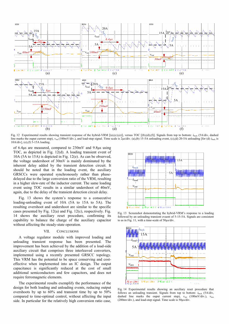
of 6.4μs are measured, compared to 230mV and 9.8μs using
TOC, as depicted in Fig. 12(d). A loading transient event of
10A (5A to 15A) is depicted in Fig. 12(e). As can be observed,
the voltage undershoot of 30mV is mainly dominated by the
inherent delay added by the transient detection circuit. It
should be noted that in the loading event, the auxiliary
GRSCCs were operated synchronously rather than phase-
delayed due to the large conversion ratio of the VRM, resulting
in a higher slew-rate of the inductor current. The same loading
event using TOC results in a similar undershoot of 40mV,
again, due to the delay of the transient detection circuit delay.
Fig. 13 shows the system’s response to a consecutive
loading-unloading event of 10A (5A to 15A to 5A). The
resulting overshoot and undershoot are similar to the specific
cases presented by Fig. 12(a) and Fig. 12(c), respectively. Fig.
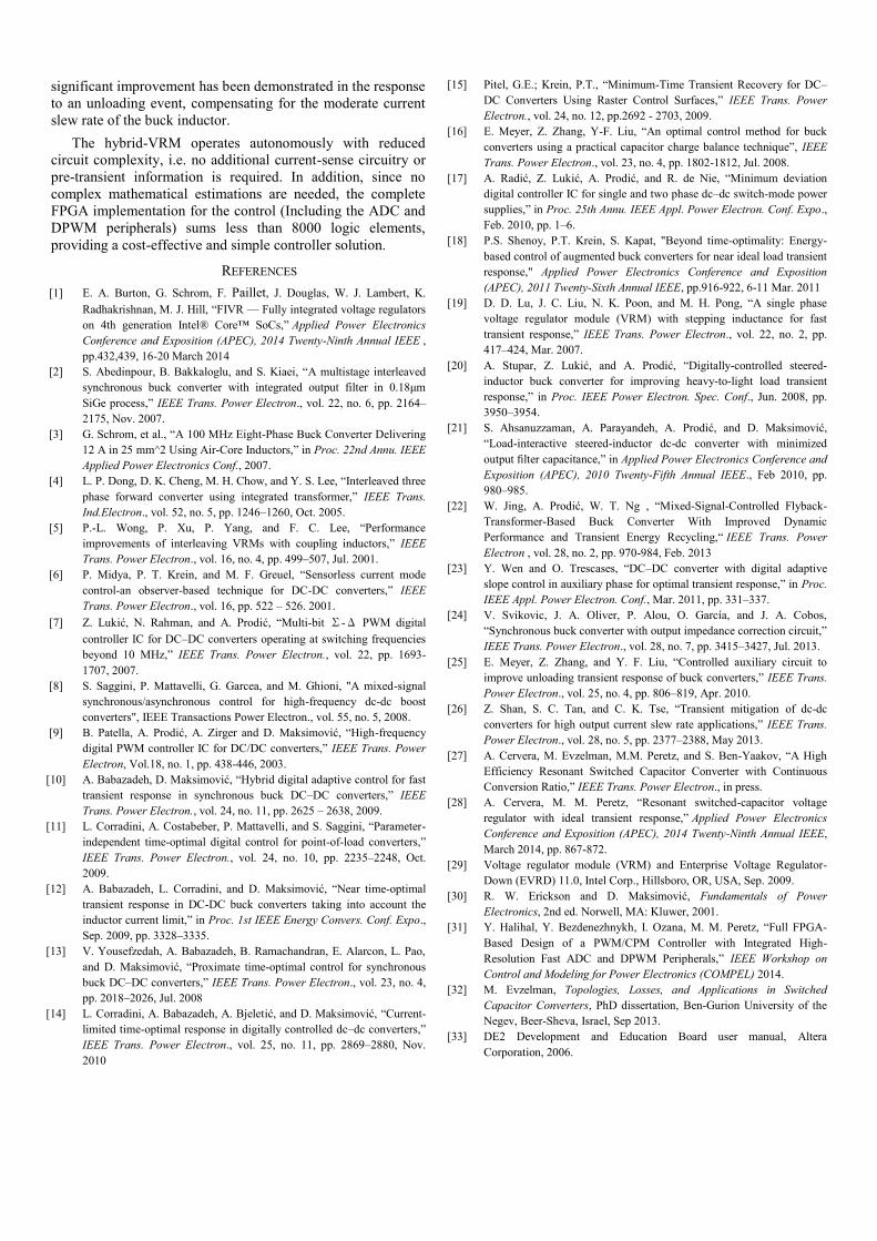
14 shows the auxiliary reset procedure, confirming its
capability to balance the charge of the auxiliary capacitor
without affecting the steady-state operation.
VII. CONCLUSIONS
A voltage regulator module with improved loading and
unloading transient response has been presented. The
improvement has been achieved by the addition of a load-side
auxiliary circuit that comprises three interleaved converters,
implemented using a recently presented GRSCC topology.
This VRM has the potential to be space conserving and cost-
effective when implemented into an IC design. The output
capacitance is significantly reduced at the cost of small
additional semiconductors and few capacitors, and does not
require ferromagnetic elements.
The experimental results exemplify the performance of the
design for both loading and unloading events, reducing output
overshoots by up to 60% and transient time by up to 50%
compared to time-optimal control, without affecting the input
side. In particular for the relatively high conversion ratio case,
(a)
ibuck
iload
20A
5A
100mV
6.4µs
vout
20A
5A
iload
230mV
9.8µs
4µs
60mV
iload
15A
5A
vout
(a)150mVvout
iload
15A
5A
8µs
(c)
(d)(b) (f)
(e)
15A
5A
vout
40mV
iload
30mV
vout
15A
5A
ibuck
ibuck
ibuck
ibuck
i buck
vout
iload
Fig. 12 Experimental results showing transient response of the hybrid-VRM [(a),(c),(e)], versus TOC [(b),(d),(f)]. Signals from top to bottom: ibuck (5A/div, dashed
line marks the ouput current step), vout (100mV/div.), and load-step signal. Time scale is 2µs/div. (a),(b) 15-5A unloading event, (c),(d) 20-5A unloading [for (d) ibuck is
10A/div], (e),(f) 5-15A loading.
Fig. 13 Screenshot demonstrating the hybrid-VRM’s response to a loading
followed by an unloading transient evaent of 5-15-5A. Signals are consistent
to as in Fig. 11, with a time-scale of 50µs/div.
Fig. 14 Experimental results showing an auxiliary reset procedure that
follows an unloading transient. Signals from top to bottom: ibuck (5A/div, dashed line marks the ouput current step), vout (100mV/div.), vaux
(200mv/div.), and load-step signal. Time scale is 50µs/div.
15A
5A
iload
ibuck
vout
15A
5A
iload
ibuck
vout
vaux
significant improvement has been demonstrated in the response
to an unloading event, compensating for the moderate current
slew rate of the buck inductor.
The hybrid-VRM operates autonomously with reduced
circuit complexity, i.e. no additional current-sense circuitry or
pre-transient information is required. In addition, since no
complex mathematical estimations are needed, the complete
FPGA implementation for the control (Including the ADC and
DPWM peripherals) sums less than 8000 logic elements,
providing a cost-effective and simple controller solution.
REFERENCES
[1] E. A. Burton, G. Schrom, F. Paillet, J. Douglas, W. J. Lambert, K.
Radhakrishnan, M. J. Hill, “FIVR — Fully integrated voltage regulators
on 4th generation Intel® Core™ SoCs,” Applied Power Electronics
Conference and Exposition (APEC), 2014 Twenty-Ninth Annual IEEE ,
pp.432,439, 16-20 March 2014
[2] S. Abedinpour, B. Bakkaloglu, and S. Kiaei, “A multistage interleaved
synchronous buck converter with integrated output filter in 0.18μm
SiGe process,” IEEE Trans. Power Electron., vol. 22, no. 6, pp. 2164–
2175, Nov. 2007.
[3] G. Schrom, et al., “A 100 MHz Eight-Phase Buck Converter Delivering
12 A in 25 mm^2 Using Air-Core Inductors,” in Proc. 22nd Annu. IEEE
Applied Power Electronics Conf., 2007.
[4] L. P. Dong, D. K. Cheng, M. H. Chow, and Y. S. Lee, “Interleaved three
phase forward converter using integrated transformer,” IEEE Trans.
Ind.Electron., vol. 52, no. 5, pp. 1246–1260, Oct. 2005.
[5] P.-L. Wong, P. Xu, P. Yang, and F. C. Lee, “Performance
improvements of interleaving VRMs with coupling inductors,” IEEE
Trans. Power Electron., vol. 16, no. 4, pp. 499–507, Jul. 2001.
[6] P. Midya, P. T. Krein, and M. F. Greuel, “Sensorless current mode
control-an observer-based technique for DC-DC converters,” IEEE
Trans. Power Electron., vol. 16, pp. 522 – 526. 2001.
[7] Z. Luki , N. Rahman, and A. Prodi , “Multi-bit Σ-Δ PWM digital
controller IC for DC–DC converters operating at switching frequencies
beyond 10 MHz,” IEEE Trans. Power Electron., vol. 22, pp. 1693-
1707, 2007.
[8] S. Saggini, P. Mattavelli, G. Garcea, and M. Ghioni, "A mixed-signal
synchronous/asynchronous control for high-frequency dc-dc boost
converters", IEEE Transactions Power Electron., vol. 55, no. 5, 2008.
[9] B. Patella, A. Prodi , A. Zirger and D. Maksimovi , “High-frequency
digital PWM controller IC for DC/DC converters,” IEEE Trans. Power
Electron, Vol.18, no. 1, pp. 438-446, 2003.
[10] A. Babazadeh, D. Maksimovi , “Hybrid digital adaptive control for fast
transient response in synchronous buck DC–DC converters,” IEEE
Trans. Power Electron., vol. 24, no. 11, pp. 2625 – 2638, 2009.
[11] L. Corradini, A. Costabeber, P. Mattavelli, and S. Saggini, “Parameter-
independent time-optimal digital control for point-of-load converters,”
IEEE Trans. Power Electron., vol. 24, no. 10, pp. 2235–2248, Oct.
2009.
[12] A. Babazadeh, L. Corradini, and D. Maksimovi , “Near time-optimal
transient response in DC-DC buck converters taking into account the
inductor current limit,” in Proc. 1st IEEE Energy Convers. Conf. Expo.,
Sep. 2009, pp. 3328–3335.
[13] V. Yousefzedah, A. Babazadeh, B. Ramachandran, E. Alarcon, L. Pao,
and D. Maksimovi , “Proximate time-optimal control for synchronous
buck DC–DC converters,” IEEE Trans. Power Electron., vol. 23, no. 4,
pp. 2018–2026, Jul. 2008
[14] L. Corradini, A. Babazadeh, A. Bjeleti , and D. Maksimovi , “Current-
limited time-optimal response in digitally controlled dc–dc converters,”
IEEE Trans. Power Electron., vol. 25, no. 11, pp. 2869–2880, Nov.
2010
[15] Pitel, G.E.; Krein, P.T., “Minimum-Time Transient Recovery for DC–
DC Converters Using Raster Control Surfaces,” IEEE Trans. Power
Electron., vol. 24, no. 12, pp.2692 - 2703, 2009.
[16] E. Meyer, Z. Zhang, Y-F. Liu, “An optimal control method for buck
converters using a practical capacitor charge balance technique”, IEEE
Trans. Power Electron., vol. 23, no. 4, pp. 1802-1812, Jul. 2008.
[17] A. Radi , Z. Luki , A. Prodi , and R. de Nie, “Minimum deviation
digital controller IC for single and two phase dc–dc switch-mode power
supplies,” in Proc. 25th Annu. IEEE Appl. Power Electron. Conf. Expo.,
Feb. 2010, pp. 1–6.
[18] P.S. Shenoy, P.T. Krein, S. Kapat, "Beyond time-optimality: Energy-
based control of augmented buck converters for near ideal load transient
response," Applied Power Electronics Conference and Exposition
(APEC), 2011 Twenty-Sixth Annual IEEE, pp.916-922, 6-11 Mar. 2011
[19] D. D. Lu, J. C. Liu, N. K. Poon, and M. H. Pong, “A single phase
voltage regulator module (VRM) with stepping inductance for fast
transient response,” IEEE Trans. Power Electron., vol. 22, no. 2, pp.
417–424, Mar. 2007.
[20] A. Stupar, Z. Luki , and A. Prodi , “Digitally-controlled steered-
inductor buck converter for improving heavy-to-light load transient
response,” in Proc. IEEE Power Electron. Spec. Conf., Jun. 2008, pp.
3950–3954.
[21] S. Ahsanuzzaman, A. Parayandeh, A. Prodi , and D. Maksimovi ,
“Load-interactive steered-inductor dc-dc converter with minimized
output filter capacitance,” in Applied Power Electronics Conference and
Exposition (APEC), 2010 Twenty-Fifth Annual IEEE., Feb 2010, pp.
980–985.
[22] W. Jing, A. Prodi , W. T. Ng , “Mixed-Signal-Controlled Flyback-
Transformer-Based Buck Converter With Improved Dynamic
Performance and Transient Energy Recycling,“ IEEE Trans. Power
Electron , vol. 28, no. 2, pp. 970-984, Feb. 2013
[23] Y. Wen and O. Trescases, “DC–DC converter with digital adaptive
slope control in auxiliary phase for optimal transient response,” in Proc.
IEEE Appl. Power Electron. Conf., Mar. 2011, pp. 331–337.
[24] V. Svikovic, J. A. Oliver, P. Alou, O. García, and J. A. Cobos,
“Synchronous buck converter with output impedance correction circuit,”
IEEE Trans. Power Electron., vol. 28, no. 7, pp. 3415–3427, Jul. 2013.
[25] E. Meyer, Z. Zhang, and Y. F. Liu, “Controlled auxiliary circuit to
improve unloading transient response of buck converters,” IEEE Trans.
Power Electron., vol. 25, no. 4, pp. 806–819, Apr. 2010.
[26] Z. Shan, S. C. Tan, and C. K. Tse, “Transient mitigation of dc-dc
converters for high output current slew rate applications,” IEEE Trans.
Power Electron., vol. 28, no. 5, pp. 2377–2388, May 2013.
[27] A. Cervera, M. Evzelman, M.M. Peretz, and S. Ben-Yaakov, “A High
Efficiency Resonant Switched Capacitor Converter with Continuous
Conversion Ratio,” IEEE Trans. Power Electron., in press.
[28] A. Cervera, M. M. Peretz, “Resonant switched-capacitor voltage
regulator with ideal transient response,” Applied Power Electronics
Conference and Exposition (APEC), 2014 Twenty-Ninth Annual IEEE,
March 2014, pp. 867-872.
[29] Voltage regulator module (VRM) and Enterprise Voltage Regulator-
Down (EVRD) 11.0, Intel Corp., Hillsboro, OR, USA, Sep. 2009.
[30] R. W. Erickson and D. Maksimovi , Fundamentals of Power
Electronics, 2nd ed. Norwell, MA: Kluwer, 2001.
[31] Y. Halihal, Y. Bezdenezhnykh, I. Ozana, M. M. Peretz, “Full FPGA-
Based Design of a PWM/CPM Controller with Integrated High-
Resolution Fast ADC and DPWM Peripherals,” IEEE Workshop on
Control and Modeling for Power Electronics (COMPEL) 2014.
[32] M. Evzelman, Topologies, Losses, and Applications in Switched
Capacitor Converters, PhD dissertation, Ben-Gurion University of the
Negev, Beer-Sheva, Israel, Sep 2013.
[33] DE2 Development and Education Board user manual, Altera
Corporation, 2006.