
Improved characterization and evaluation measurements for ... · 7...
188
NAT L INST OF ST4N0 & TECH R.I.C. AlllDM Efi7D3b a c NIST PUBLfCATIONS NIST SPECIAL PUBLICATION 400-94 U.S. DEPARTMENT OF COMMERCE/Technology Administration National Institute of Standards and Technology or Measurement Technolo. Improved Characterization and Evaluation Measurements for HgCdTe Detector Materials, Processes, and Devices Used on the GOES and TIROS Satellites U57 NO. ^00-91 199^1
Transcript of Improved characterization and evaluation measurements for ... · 7...

NAT L INST OF ST4N0 & TECH R.I.C.
AlllDM Efi7D3b
a
c
NIST
PUBLfCATIONS
NIST SPECIAL PUBLICATION 400-94
U.S. DEPARTMENT OF COMMERCE/Technology Administration
National Institute of Standards and Technology
or Measurement Technolo.
Improved Characterization and Evaluation Measurements
for HgCdTe Detector Materials, Processes, and Devices
Used on the GOES and TIROS Satellites
U57
NO. ^00-91
199^1
7he National Institute of Standards and Technology was established in 1988 by Congress to "assist
industry in the development of technology . . . needed to improve product quality, to modernize
manufacturing processes, to ensure product reliability . . . and to facilitate rapid commercialization ... of
products based on new scientific discoveries."
NIST, originally founded as the National Bureau of Standards in 1901, works to strengthen U.S.
industry's competitiveness; advance science and engineering; and improve public health, safety, and the
environment. One of the agency's basic functions is to develop, maintain, and retain custody of the national
standards of measurement, and provide the means and methods for comparing standards used in science,
engineering, manufacturing, commerce, industry, and education with the standards adopted or recognized
by the Federal Government.
As an agency of the U.S. Commerce Department's Technology Administration, NIST conducts basic
and applied research in the physical sciences and engineering and performs related services. The Institute
does generic and precompetitive work on new and advanced technologies. NIST's research facilities are
located at Gaithersburg, MD 20899, and at Boulder, CO 80303. Major technical operating units and their
principal activities are listed below. For more information contact the Public Inquiries Desk, 301-975-3058.
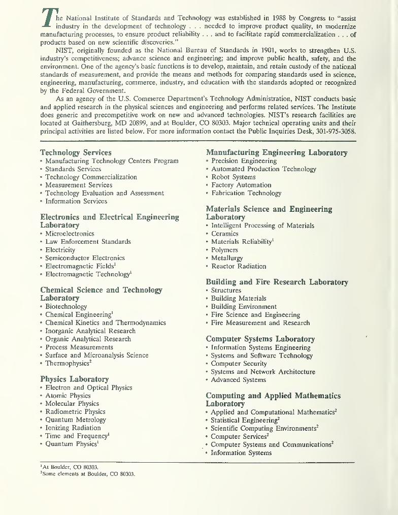
Technology Services• Manufacturing Technology Centers Program• Standards Services
• Technology Commercialization
• Measurement Services
• Technology Evaluation and Assessment• Information Services
Electronics and Electrical EngineeringLaboratory• Microelectronics
• Law Enforcement Standards
• Electricity
• Semiconductor Electronics
• Electromagnetic Fields'
• Electromagnetic Technology'
Chemical Science and TechnologyLaboratory• Biotechnology
• Chemical Engineering'
• Chemical Kinetics and Thermodynamics• Inorganic Analytical Research• Organic Analytical Research• Process Measurements• Surface and Microanalysis Science
• Thermophysics^
Physics Laboratory• Electron and Optical Physics
• Atomic Physics
• Molecular Physics
• Radiometric Physics
• Quantum Metrology• Ionizing Radiation
• Time and Frequency'
• Quantum Physics'
Manufacturing Engineering Laboratory• Precision Engineering
• Automated Production Technology• Robot Systems
• Factory Automation• Fabrication Technology
Materials Science and EngineeringLaboratory• Intelligent Processing of Materials
• Ceramics
• Materials Reliability'
• Polymers
• Metallurgy
• Reactor Radiation
Building and Fire Research Laboratory• Structures
• Building Materials
• Building Environment• Fire Science and Engineering
• Fire Measurement and Research
Computer Systems Laboratory• Information Systems Engineering
• Systems and Software Technology• Computer Security
• Systems and Network Architecture
• Advanced Systems
Computing and Applied MathematicsLaboratory• Applied and Computational Mathematics^• Statistical Engineering^
• Scientific Computing Environments^
• Computer Services^
• Computer Systems and Communications^
• Information Systems
'At Boulder, CO 80303.
^Some elements at Boulder, CO 80303.
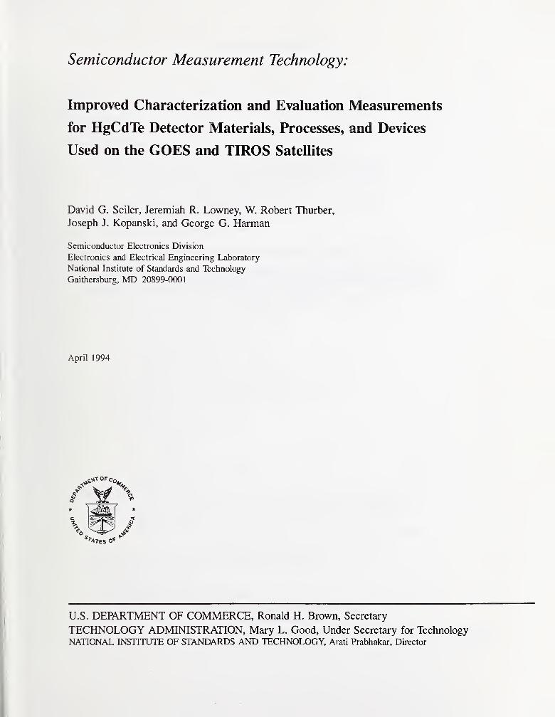
Semiconductor Measurement Technology:
Improved Characterization and Evaluation Measurements
for HgCdTe Detector Materials, Processes, and Devices
Used on the GOES and TIROS Satellites
David G. Seller, Jeremiah R. Lowney, W. Robert Thurber,
Joseph J. Kopanski, and George G. Harman
Semiconductor Electronics Division
Electronics and Electrical Engineering Laboratory
National Institute of Standards and Technology
Gaithersburg, MD 20899-0001
April 1994
U.S. DEPARTMENT OF COMMERCE, Ronald H. Brown, Secretary
TECHNOLOGY ADMINISTRATION, Mary L. Good, Under Secretary for Technology
NATIONAL INSTITUTE OF STANDARDS AND TECHNOLOGY, Arati Prabhakar, Director
National Institute of Standards and Technology Special Publication 400-94
Natl. Inst. Stand. Technol. Spec. Publ. 400-94, 184 pages (April 1994)
CODEN: NSPUE2
U.S. GOVERNMENT PRINTING OFFICEWASHINGTON: 1994
For sale by the Superintendent of Documents, U.S. Government Printing Office, Washington, DC 20402-9325
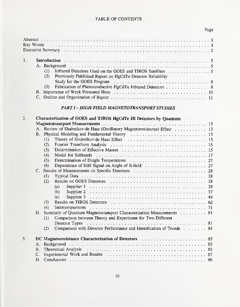
TABLE OF CONTENTS
Page
Abstract 1
Key Words 1
Executive Summary 2
1. Introduction 5
A. Background 5
(1) Infrared Detectors Used on the GOES and TIROS Satellites 5
(2) Previously Published Report on HgCdTe Detector Reliability
Study for the GOES Program 8
(3) Fabrication of Photoconductive HgCdTe Infrared Detectors 8
B. Importance of Work Presented Here 10
C. Outline and Organization of Report 11
PART I - HIGH-FIELD MAGNETOTRANSPORTSTUDIES
2. Characterization of GOES and TIROS HgCdTe IR Detectors by QuantumMagnetotransport Measurements 13
A. Review of Shubnikov-de Haas (Oscillatory Magnetoresistance) Effect 13
B. Physical Modeling and Fundamental Theory 13
(1) Theory of Shubnikov-de Haas Effect 13
(2) Fourier Transform Analysis 15
(3) Determination of Effective Masses 15
(4) Model for Subbands 17
(5) Determination of Dingle Temperatures 27
(6) Dependence of SdH Signal on Angle of B-field 27
C. Results of Measurements on Specific Detectors 28
(1) Typical Data 28
(2) Results on GOES Detectors 28
(a) Supplier 1 28
(b) Supplier 2 37
(c) Supplier 3 49
(3) Results on TIROS Detectors 62
(4) Intercomparisons 71
D. Summary of Quantum Magnetotransport Characterization Measurements 81
(1) Comparison between Theory and Experiment for Two Different
Detector Types 81
(2) Comparison with Detector Performance and Identification of Trends 84
3 . DC Magnetoresistance Characterization of Detectors 85
A. Background 85
B. Theoretical Analysis 85
C. Experimental Work and Results 87
D. Conclusions 96
iii

TABLE OF CONTENTS (Continued)
Page
PART II -OTHER CHARACTERIZATION STUDIES
4. Bonding, Metallization, and Packaging for GOES and TIROS Infrared Detectors . . . 97
A. Overview and Rationale 97
B. Accomplishments 98
C. Recommended Practice for Wire Bonding and Metallization Used in
Radiation Detectors Prepared for Use in GOES, TIROS, and Other Satellites 99
D. Glossary 101
E. Typical Bonding Characteristics and Appearance of Plated Gold Films 102
5. Semiconductor Electronic Test Structures: Appiications to Infrared Detector
Materials and Processes 103
A. Introduction 103
B. Conclusions 105
6. Scanning Capacitance Microscopy: A Nondestructive Characterization Tool 106
A. Background 106
B. Applications of SCM to GOES and Related Infrared Detectors 106
C. Establishment of Facility 107
D. Preliminary Results 109
E. Summary 113
7. NIST Review of the GOES Calibration Program 114
A. Purpose 114
B. Summary of Visits to Facilities 114
C. Recommendations 115
8. Summary and Conclusions 117
A. Magnetotransport Measurements 117
B. Other Characterization Studies 118
9. References 120
APPENDICES
A. Reprint of Published Paper "Heavily Accumulated Surfaces of Mercury CadmiumTelluride Detectors: Theory and Experiment"
B. Reprint of Published Paper "Review of Semiconductor Microelectronic Test Structures
with Applications to Infrared Detector Materials and Processes"
C. Reprint of Published Paper "Hgi.^Cd^Te Characterization Measurements: Current
Practice and Future Needs"
IV

LIST OF FIGURES
Page
1 . 1 Principal components of a HgCdTe GOES detector element 9
2.1a Built-in potential for accumulation layer with total electron density of 8.9 x 10^^ cm'^
and alloy fraction x = 0.191 21
2.1b "E versus k" dispersion relations for the subbands for this potential, showing
spin-splitting 22
2.2a Electron density computed by solving Poisson's equation for a charge continuimi
and from full quantum-mechanical calculations for the case of figure 2.1b 23
2.2b Calculated subband densities as a function of total density 24
2.3a Subband Fermi energies as a function of total density, measured from the bottom
of each subband 25
2.3b Ratio of subband cyclotron effective masses to the free electron mass at the Fermi
energy as a function of total density 26
2.4 The ac and dc signals of the magnetoresistance of a typical detector element, 31 IB 29
2.5 The ac signal for detector element 311 IB showing the oscillations imposed on a
background which initially rises abruptly and then falls slowly 30
2.6 The ac signal which has been centered by doing a spline fit to the average value of
regions of the original signal and then replotting the signal relative to the fit 31
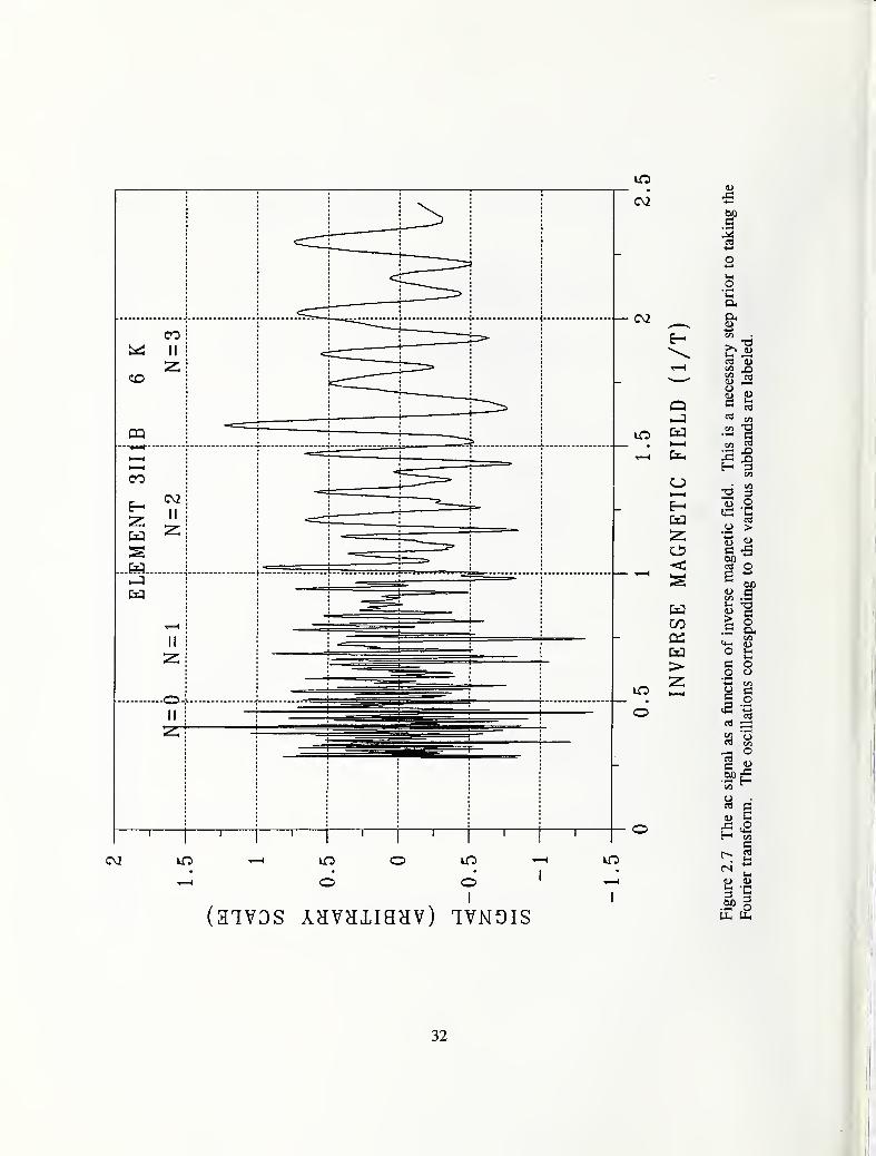
2.7 The ac signal as a function of inverse magnetic field 32
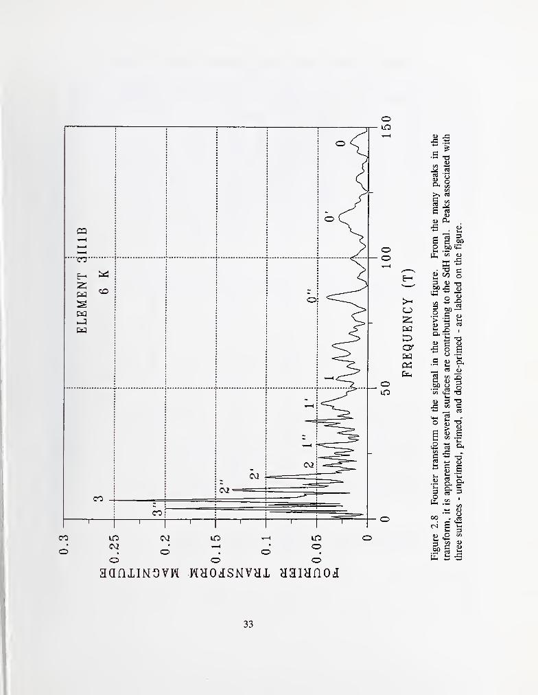
2.8 Fourier transform of the signal in the previous figure 33
2.9 Fourier transforms from elements of two different Supplier 1 detectors, 1 and 2 34
2.10 Subband carrier density versus total density for the Supplier 1 detector elements in
figure 2.9 38
2.11 Shubnikov-de Haas traces of four elements of detector 2III1 from Supplier 2 39
2.12 Temperature dependence of the SdH oscillations of element 2III IB 40
2.13 Traces of four elements of detector 2III2 41
2.14 Fourier transforms for the elements of detector 2III1 42
V

LIST OF FIGURES (Continued)
Page
2.15 Fourier transforms for the elements of detector 2III2 44
2.16 Results of rotating element 2III1B in the magnetic field 45
2.17 Shubnikov-de Haas oscillations from the three Supplier 2 detectors fabricated for
diagnostic purposes 46
2.18 Fourier transforms of the SdH response in figure 2.17 for the experimental
Supplier 2 detectors 47
2.19 Response curves for the two types of Supplier 3 detectors 50
2.20 Temperature dependence of the SdH response of a Supplier 3 type I element, 3I2A .... 51
2.21 Fourier transforms of the temperature data in figure 2.20 52
2.22 Fourier transforms from five type I detector elements from Supplier 3 53
2.23 Temperature dependence of the response of element 311 IC from a Supplier 3 type II
detector 57
2.24 Fourier transforms of four elements of a Supplier 3 type II detector 58
2.25 Subband carrier density as a function of total density for the Supplier 3 type I
detector elements listed in table 2.3 61
2.26 Subband carrier density as a function of total density for the Supplier 2 and
Supplier 3 type II detector elements listed in tables 2.2 and 2.4, respectively 63
2.27 Response of element 3I2A when rotated in the magnetic field 64
2.28 Fourier transforms of the rotation traces in the previous figure 65
2.29 Normalized frequency dependence of the Fourier transform peaks for the major
subbands of element 3I2A as a function of the angle of rotation in the magnetic
field 66
2.30 Comparison of synthesized and original data for element 3I2A 67
2.31 Reconstruction of the complicated SdH response for element 311 IB 68
2.32 Shubnikov-de Haas response of six TIROS detectors 69
2.33 Fourier transforms of the six TIROS detectors in the previous figure 70
vi
LIST OF FIGURES (Continued)
Page
2.34 Shubnikov-de Haas traces for detector T56238 at five temperatures 74
2.35 Fourier transforms of the SdH traces in the previous figure 75
2.36 Subband density as a function of total density for the six TIROS detectors discussed
in this section 76
2.37 Fit to determine the effective mass for subband 0' 77
2.38 Illustration of the determination of the Dingle temperature Tj) 78
2.39 Representative SdH traces from each supplier and commercial detector type 79
2.40 Fourier transforms of the SdH traces in figure 2.39 80
2.41a Fourier transform of SdH data for detector element 3I2A; the label "H" stands for
harmonic; peaks are labeled by subband number 82
2.41b Fourier transform of SdH date for detector element 3II1B; the peaks are labeled by
subband number 83
3.1 Relative resistance as a function of ijlB for different length-to-width ratios a,
from reference 3.8 86
3.2 Illustration of a typical photoconductive HgCdTe infrared detector 88
3.3 Two-terminal transverse magnetoresistance as a function of B for a type I
passivated detector and a type II passivated detector at 6 K 90
3.4 Expanded scale of the low-field behavior of the transverse magnetoresistance as a
function of B for type I and type II detectors at 6 K and 77 K 91
3.5 Two-terminal transverse magnetoresistance as a function of B for a type III passivated
detector at 6 K 92
3.6 Expanded scale of the low-field behavior of the transverse magnetoresistance as a
function of B for a type III detector at 6 and 77 K 93
3.7 Two-terminal transverse magnetoresistance as a function of B for a multi-element
type III detector at 6 K 94
6.1 Digital Instruments Inc. Nanoscope III atomic force microscope with a large sample
stage similar to the system operational at NIST 108
vii
LIST OF FIGURES (Continued)
Page
6.2 Low-magnification AFM image showing parts of three photoconductive detectors ..... 110
6.3 Cross-sectional analysis of an AFM image of the boundary between the passivated
active layer and the metal pad of a detector element Ill
6.4 Atomic force microscopy image of the edge of a photoconductive detector revealing fme
structure in the topography clustered at the edge of the active area 112
LIST OF TABLES
Page
1 . 1 Imager Channel Functions 6
1.2 Partial Listing of Spaceborne Infrared Sensor Programs Using Mercury-Cadmium-
Telluride Detectors 7
2.1 Results of Shubnikov-de Haas Analysis for Supplier 1 Detectors 35
2.2a Results of Shubnikov-de Haas Analysis for Supplier 2 Detector 43
2.2b Results of Shubnikov-de Haas Analysis for Supplier 2 Experimental Detectors 48
2.3 Results of Shubnikov-de Haas Analysis for Supplier 3 Type I Detectors 54
2.4 Results of Shubnikov-de Haas Analysis for Supplier 3 Type II Detectors 59
2.5 Results of Shubnikov-de Haas Analysis for TIROS Detectors 72
3.1 Parameter Values Extracted by the Transverse Magnetoresistance Method 95
viii
Semiconductor Measurement Technology :
Improved Characterization and Evaluation Measurements
for HgCdTe Detector Materials, Processes, and Devices
Used on the GOES and TIROS Satellites
D. G. Seller, J. R. Lowney, W. R. Thurber,
J. J. Kopanski, and G. G. Harman
Semiconductor Electronics Division
National Institute of Standards and Technology
Gaithersburg, MD 20899
ABSTRACT
An extensive study was carried out to improve the characterization and evaluation
methods used for HgCdTe (mercury-cadmium-telluride) photoconductive infrared
detectors used in GOES and TIROS satellites. High-field magnetotransport techniques
were used to determine the electrical properties of the detector accumulation layers,
which partially control their detectivities. Assessments were made of the quality of the
bonding and packaging used in detector fabrication, and a list of recommended practices
was produced. The applicability of scanning capacitance microscopy and test structures
to detector-array evaluation is discussed, and, finally, recommendations are made for
standardized detector calibration. The results of this work have provided new and more
refined measurement methods that can be adopted by the detector manufacturers to
improve performance and yield.
KEY WORDS: bonding; geostationary environment satellite; infrared detector; IR
detector calibration; magnetoresistance; mercury cadmium telluride; packaging;
scanning probe microscopy; Shubnikov-de Haas; test structure
Disclaimer: Certain commercial equipment, instruments, or materials are identified in
this report in order to specify the experimental procedure adequately. Such
identification does not imply recommendation or endorsement by the National Institute
of Standards and Technology, nor does it imply that the materials or equipment
identified are necessarily the best available for the purpose.
1
EXECUTIVE SUMMARY
This report summarizes results of extensive studies carried out by the National Institute of Standards
and Technology (NIST) for the National Oceanic and Atmospheric Administration (NOAA) on
improving characterization and evaluation measurements of HgCdTe infrared detector materials,
processes, and devices used for the Geostationary Operational Environmental Satellite (GOES) and the
Television and Infrared Operational Satellite (TIROS) systems.
NIST has provided services to NOAA, the National Aeronautics and Space Administration (NASA),
ITT Aerospace Communications Division in Fort Wayne, Indiana, and several other detector
fabrication companies in areas of detector packaging, bonding, and metallization. Numerous detector
committee meetings and briefings were attended by NIST personnel.
The techniques developed by NIST and reported here have the advantage that they can be applied to
actual, small-area, commercial detectors being manufactured for the GOES and TIROS Programs.
These measurements provide high-quality data which are demonstrated to provide a unique
characterization signature for an infrared detector. A physical model of the detector surface layers
has been developed relating detector parameters to performance, thus permitting a better
understanding and engineering of current detectors as well as future generations. In addition, the
techniques developed here provide a diagnostic tool to characterize effects of processing on detector
performance, as well as the ability to characterize detector stability and reliability. New processing
fabrication procedures being developed can now be much better understood and monitored.
NIST has carried out state-of-the-art applied and fundamental research on two magnetic-field-based
characterization measurements needed for the HgCdTe-based infrared photoconductive detectors of the
GOES and TIROS Programs. The oscillatory variation in resistance with magnetic field, i.e., the
Shubnikov-de Haas (SdH) effect, and the behavior of the dc magnetoresistance are both shown to
provide crucial understanding and characterization of the properties (electron concentrations and
mobilities) of the two-dimensional electron gas (2DEG) in the accumulation layers produced by the
passivation process. The detector performance depends to a great extent upon the type and quality of
the passivation process. Ten samples were prepared for low-temperature Shubnikov-de Haas and
other measurements for the NIST HgCdTe detector studies.
Shubnikov-de Haas oscillations in the transverse magnetoresistance have been used to characterize
accumulation layers of the infrared detectors used in GOES and TIROS weather satellites. Electron
densities, cyclotron effective masses, and Dingle temperatures can be obtained from the data for each
subband in the 2D electron gas formed by the accumulation layer. A first-principles calculation of the
subband energy dispersion relations has been performed in order to compare theory and experiment.
The model is needed to extract the electron density from the data because the energy bands are very
nonparabolic in narrow-gap HgCdTe. The agreement between predicted and measured masses and
Fermi energies was excellent for anodically oxidized layers. Effective masses could not be obtained
for other processes because signals were weak and complex. A large number of detectors from each
of three suppliers were measured by the SdH effect, and the data were analyzed. Results obtained for
devices with type I passivation (anodic oxidation) gave Fourier transforms with large, well-defined
peaks from which the carrier density of the accumulation layer was obtained. Detector elements with
different passivations, type II and type III, had a weak SdH response. The carrier density of
accumulation layers of type II and III detectors were much greater than those for type I detectors.
The generally lower mobilities and higher densities of accumulation layers in type II and type III
detectors led to their improved performance because of reduced leakage and decreased surface
recombination. Angular rotation studies were done on devices from two suppliers to verify that the
SdH signal was coming from the two-dimensional accumulation layers. Effective masses and Dingle
temperatures were calculated for one or more elements with type I passivation. The values were in
good agreement with theoretical calculations.
A new and simpler method to characterize infrared detectors has been developed based on dc
magnetoresistance upon which the small-amplitude SdH oscillations are superimposed. Electron
density and mobility in the top accumulation layer can be determined from the magnetic-field
dependence of the transverse magnetoresistance at high fields. Agreement between densities and
mobilities in accumulation layers of type I and type II detectors with Hall measurement data supplied
by the manufacturers showed the method was accurate. Measurements were made on a large number
of detectors. The results showed variability of the accumulation-layer density by 20% among three
elements of a multi-element detector. This method can be applied directly to the fabricated detectors
because it requires only two terminals.
A total of six visits were made to three GOES and TIROS infrared detector manufacturers during
fiscal years 1992 and 1993. The first visit to each site served to evaluate the production lines and the
processes. Later visits were made to help them improve the detector packaging. This included one
2.5-h seminar on wire bonding and reliability of metallurgical systems used in packaging HgCdTedetectors. Over 30 people attended that seminar. For another company, a more informal hour-long
presentation was made to 6 or 7 engineers and management personnel. Extra time was later spent in
visiting their packaging laboratories. A scanning electron microscope study was made of detectors
from one manufacturer that showed several defects (the results of this study were presented at a
GOES project review at NASA Goddard, July 10, 1992). This information, with proposed solutions,
was also fed back to the manufacturer to help them improve their product. Studies were carried out
at NIST and at two detector manufacturing sites to establish the best molecular-cleaning methods that
are compatible with normal HgCdTe detector packaging methods. For this work, ultraviolet cleaning
equipment was handcarried to detector manufacturers so that tests could be performed there.
Because of the substantial impact of test structures on other semiconductor circuits, the current
state-of-the-art applications of test structures to HgCdTe-based IR detectors were comprehensively
reviewed. To place these applications in context, the general principles of applying test structures,
determined through experience with silicon integrated circuits (ICs) and GaAs monolithic microwave
integrated circuits (MMICs), were also reviewed. From these two reviews, principles and ideas were
extracted for test-structure applications that could be used to further enhance the manufacturability,
yield, and performance of IR detectors. To communicate and encourage application of test structures,
the results of the study were presented at the Measurement Techniques for Characterization of MCTMaterials, Processes, and Detectors Workshop held in Boston, Massachusetts, during October 1992
and published in Semiconductor Science and Technology. A reprint of this paper is included in this
report as an appendix.
Scanning capacitance microscopy (SCM) is a new, nondestructive metrology tool that merges a high-
sensitivity capacitance sensor with an atomic force microscope (AFM). SCM applications that could
be expected to have a large impact on the quality, yield, and manufacturability of IR detectors
include: nondestructive diagnosis of material variations within the active regions of detectors,
nondestructive prefabrication materials evaluation, and depth profiling of dopants in nanostructures.
AFM images were made of some photoconductive detector elements to illustrate the feasibility,
3
potential resolution, and image quality of SCM applied to IR detectors.
NIST staff from the Radiometric Physics Division visited and examined the radiometric calibration
programs of the detector suppliers and the system integration contractor where the final radiometric
calibrations are performed. NIST recommends that a fundamental calibration program be established
that is coordinated between the different manufacturers and assemblers. NIST also recommends that
the GOES detectors be calibrated several times before launch to establish a calibration history and
base line.
4
1. INTRODUCTION
A. Background
(1) Infrared Detectors Used on the GOES and TIROS Satellites
The National Oceanic and Atmospheric Administration (NOAA) has the responsibility for producing,
launching, and operating a multiple Geostationary Operational Environmental Satellite (GOES)system. The primary purpose of the GOES Program is the continuous and reliable collection of
environmental data in support of weather forecasting and related services. The data obtained by the
GOES satellites provide information needed for severe storm detection, monitoring, and tracking;
wind measurements from cloud motion; sea surface thermal feamres; precipitation estimates; frost
monitoring; rescue operations; and research. The geostationary orbit of these satellites allows
continuous observation of a portion of the earth and its atmosphere. Since 1974, these GOESsatellites have been used to collect and disseminate environmental data for the United States National
Weather Service. At present, there is only one aging satellite, GOES H or (GOES-7), in orbit. The
United States National Weather Service now relies heavily on this aging satellite GOES-7 for crucial
weather information.
New weather satellites are being produced by a program known as GOES-NEXT, for the next
generation of Geostationary Operational Environmental Satellites. A series of five satellites,
designated by the letters I-M, are scheduled to be produced. There are significant differences
between the GOES I-M series satellites and the earlier series. The GOES D-H satellites had a
passive, spin-stabilized, attitude control system. The GOES I-M series of satellites uses a three-axis
attitude control system. Unlike the GOES D-H series, the GOES I-M satellites support separate
imager and sounder instruments that operate independently and simultaneously perform imaging and
sounding operations. These satellites perform a number of functions including visible and infrared
imaging (Imager) and atmospheric sounding (i.e., depth profiling of the atmosphere) (Sounder) by
using various types of detectors.
The GOES sensors provide two-dimensional cloud and temperature imagery in both visible and
infrared spectra, radiometric data that provide the capability to determine the three-dimensional
structure of atmospheric temperature and water-vapor distribution, and solar and near-space
environmental data. Three different types of detectors are used in each of the Imager and Sounder
systems: silicon (Si) photovoltaic detectors for visible radiation, indium-antimonide (InSb)
photovoltaic detectors for infrared radiation, and mercury-cadmium-telluride (HgCdTe)
photoconductive detectors for various infrared-radiation spectral regions. There are five channels for
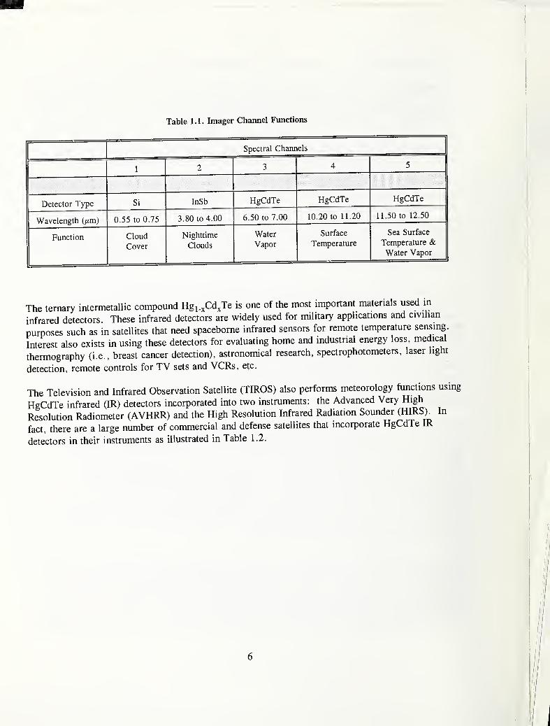
the Imager. Table 1.1 shows their specifications for detector type, wavelength range, and their
purpose. Spectral separation in the Imager is done by fixed dichroic beam splitters, permitting
simultaneous sampling of all five spectral channels.
The Sounder instrument has 19 channels. There are four Sounder bands containing Si detectors for
the visible, InSb detectors for the shortwave infrared, and HgCdTe detectors for both the midwave
and longwave infrared regions. These bands provide information on atmospheric temperature
profiling. The visible spectrum and the three infrared bands are separated by dichroic beam splitters.
The three infrared bands then pass through three concentric rings of a filter wheel where channel
filters provide sequential sampling of the seven longwave, five midwave, and six shortwave channels.
5
1
Table 1.1. Imager Charaiel Fmictions
Spectral Channels
1 2 3 4 5
Detector Type Si InSb HgCdTe HgCdTe HgCdTe
Wavelength (/xm) 0.55 to 0.75 3.80 to 4.00 6.50 to 7.00 10.20 to 11.20 11.50 to 12.50
Function Cloud
Cover
Nighttime
Clouds
Water
Vapor
Surface
Temperature
Sea Surface
Temperature &Water Vapor
The ternary intermetallic compound Hgi.,CdJe is one of the most important materials used in
infrared detectors. These infrared detectors are widely used for military applications and civilian
purposes such as in satellites that need spaceborne infrared sensors for remote temperature sensing.
Interest also exists in using these detectors for evaluating home and industrial energy loss, medical
thermography (i.e., breast cancer detection), astronomical research, spectrophotometers, laser light
detection, remote controls for TV sets and VCRs, etc.
The Television and Infrared Observation Satellite (TIROS) also performs meteorology functions using
HgCdTe infrared (IR) detectors incorporated into two instruments: the Advanced Very High
Resolution Radiometer (AVHRR) and the High Resolution Infrared Radiation Sounder (HIRS). In
fact, there are a large number of commercial and defense satellites that incorporate HgCdTe IR
detectors in their instruments as illustrated in Table 1.2.
\
6
1
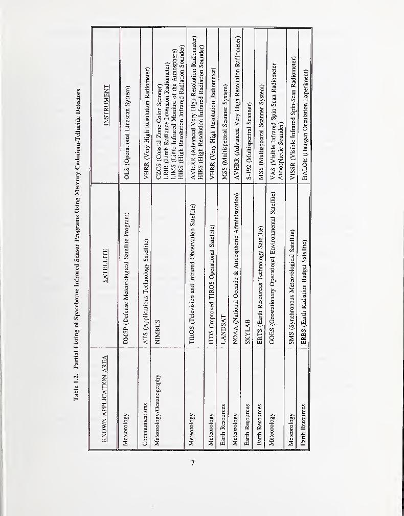
Z
D
Z
-J
<C/O
<a:<zo
<Uo,
<Z
oz
>1
gon
O
00
oo
O
00
oc
<
<
00D
Z
00o
00o
— 2
o
c
aj
00OOS
00
o
T3
co
1)
00
1)Q.O00Oas
D.E
ooO
00o
oo
0000
<00az<
T3
as
co
aJ
x:00
cE•a<
oE
coc3
Z<Oz
00o
OS
<
oo
ca00
00o
3oDas
t;
B00HasW
o
ooo
D.00
a 'D
" 00
Is> cx
< E> <
>c
O£^
Co
O00tuoo
00
oO
00
00
00o
3O0)
as
7

(2) Previously Published Report on HgCdTe Detector Reliability Study for the GOES Program
The results of a special assessment carried out by NIST, at the request of NOAA, of the reliability of
certain infrared detectors for the Geostationary Operational Environmental Satellite system were
summarized in a special report, NISTIR 4687, by D. G. Seller, G. G. Harman, J. R. Lowney, S.
Mayo, and W. S. Liggett, Jr. [1.1]. The data made available by ITT on detector resistances and
signals supported the conclusion that degradation of some detector responses had occurred, even when
the estimated measurement uncertainty was included. Statistical analysis of the 11-jwm detectors
confirmed that one detector decreased in signal with time. The existing data available to NIST are
not sufficient to identify uniquely the cause of degradation or unstable behavior present in a number
of detectors. NIST's physical examination of several detectors by optical and SEM microscopy
methods and an examination and analysis of the Detector Measurement Database has yielded several
plausible possible mechanisms for the observed degradation. These possible mechanisms are related
to the detector fabrication or processing steps and include: incomplete or poor passivation
procedures, excess mercury diffusion resulting from the ion-beam milling fabrication step, poor
indium electrical contacts produced by the indium-plating fabrication step, and delamination of the
ZnS anti-reflection optical coating. Other observed problems were poor wire bonding, use of tin-lead
solder to couple the fine gold wire (bonded to the detector) to the package terminal, and use of
silicone RTV to stake the bond wires to the edge of the ZnS substrate.
One of the recommendations given at the end of this assessment report suggested that magnetic-field-
based measurements such as Hall-effect and Shubnikov-de Haas effect measurements be performed to
determine the properties of the accumulation layers produced by the passivation process. The work
presented here addresses this recommendation.
(3) Fabrication of Photoconductive HgCdTe Infrared Detectors
Infrared photoconductive detectors are devices that convert electromagnetic radiation to electric
signals by direct conversion of incident photons into conducting electrons or holes. The signals can
then be processed to obtain information from the intensity and wavelength distribution of the incident
radiation. Figure 1.1 shows the principal elements of the HgCdTe GOES detectors [1.2].
There are a number of reasons why Hgj.^Cd^Te alloys are used. By varying the mole fraction x, the
energy gap can be continuously adjusted from below 0.04 to above 1.3 eV, covering the 1- to 25-fim
infrared region. Tailor-made materials can thus be grown to respond to preselected wavelengths,
providing one the opportunity to make a range of temperature measurements from orbit. Quantumefficiencies approaching 100% for 12- to 16-/xm-thick devices are possible. Material having a long
carrier lifetime can be produced even at relatively high processing temperatures. The material can
also be made quite pure (approaching electrical levels of approximately 1 x 10^'* cm'^ carriers). In
addition, the surfaces can be passivated by any of a large number of approaches, including using ZnS,
native (anodic) oxides, sulphides, fluorides, etc. It is important to note that the performance of the
detector depends to a great extent upon the type of passivation process.
Important factors that influence the responsivity, impedance, and noise of the photoconductive
detectors are the energy gap, doping concentration, electron and hole mobilities, carrier lifetimes,
passivation properties, the effects of ion millings, and the contacts. Effects associated with the device
contacts and surfaces can cause gross distortions of the detector operating characteristics. The
processing details for fabricating contacts to HgCdTe are based largely upon empiricism. A
8
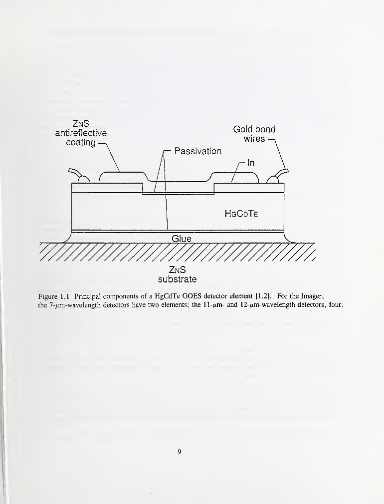
ZnSantireflective
coating
Gold bondwires
Passivation
r \
HgCdTe
Glue
ZnSsubstrate
Figure 1.1 Principal components of a HgCdTe GOES detector element [1.2]. For the Imager,
the 7-/im-wavelength detectors have two elements; the 11-^m- and 12-/Lim-wavelength detectors, four.
9

fundamental understanding is lacking. Formation of Schottky barriers causes voltage instabilities and
problems with reproducibility and reliability.
Passivation is used to produce high carrier densities at the detector surfaces to reduce recombination
and noise by repelling minority carriers and filling surface traps. Passivation also serves to stabilize
the surfaces. An adequate passivation layer must (1) be a good insulator, (2) adhere sufficiently well
to the HgCdTe, (3) be time stable, (4) be stable against the atmosphere (unless a hermetic seal is
used), (5) not be attacked by chemicals necessary for making the device, (6) be sufficiently nonporous
that atmospheric gases cannot move through it and attack the HgCdTe, and (7) produce an interface
which is sufficiently inert electrically so that it does not degrade the operation of the detector.
Inhomogeneity or nonuniformity in the relative concentrations of mercury and cadmium, doping
concentration level, or defects throughout the wafers can cause problems. Production yields for the
high-performance detectors are typically low, on the order of 5 to 10% or even lower.
B. Importance of Work Presented Here
The HgCdTe infrared detectors used in the GOES and TIROS Satellite Programs are essential
components of the satellite. The success or failure of the many functions of these satellites depends
upon the proper and reliable operation of these detectors. The detectors planned for use must have
high reponsivities or detectivities along with low 1/f noise characteristics in order to meet
specifications required by NOAA.
These state-of-the-art detectors are not easy to manufacture, and production yields are correspondingly
very low. In addition, it may be that "hot" detectors, i.e., those that meet the stringent specifications,
are more susceptible to degradation or reliability problems because of the use of newer technologies.
It is, thus, imperative that a physically based understanding, rather than just empirically based
knowledge, be acquired for the selection, operation, and determination of the limitations and
reliability of the detectors.
The GOES detector degradation task force team "struggled" with the question of how to characterize
and understand the stability or reliability of the photoconductive detectors. A significant diagnostic
technique was found to be lacking. The development of the magnetotransport methods presented here
now provides a diagnostic tool to be used.
The HgCdTe industry is very concerned about the following issues that were directly raised by
several companies:
• "Why do individual detectors fail? Local characterization techniques are needed. There is no
well-understood body of knowledge available for HgCdTe. In wide-gap HgCdTe, one obtains
good signatures by photoluminescence methods, but in narrow-gap material, understanding of the
issues and characterization methods is lacking."
• "Many issues exist: nonuniform impurity distributions, defects and impurities, complexes, ...
We don't know how to analyze the structures we are growing. THE ABILITY TO GROWSTRUCTURES HAS OUTGROWN THE ABILITY TO CHARACTERIZE THE MATERIAL.There is a need to develop a good signature by using a particular characterization technique."
• Producing high-performance detectors is still a "trial and error" process using "black magic" and
10
"lots of sweat." Industry has to "build a learning curve" first.
NIST has thus investigated, developed, and performed state-of-the-art applied and fundamental
research related to new and improved characterization measurements for HgCdTe-based infrared
detectors needed by the GOES and TIROS Programs. NIST has developed a number of magnetic-
field-based techniques that have the proven capabilities of providing the necessary understanding and
characterization of HgCdTe detectors. These techniques include: (1) variable magnetic field and
variable-temperature magnetotransport measurements, and (2) oscillatory magnetoresistance (periodic
variation of resistance with magnetic field), i.e., Shubnikov-de Haas measurements. These techniques
are capable of determining the necessary information about the properties of the two-dimensional
electron gas (2DEG) in the accumulation layers produced by the passivation process and of the bulk
HgCdTe. This information includes the concentrations and mobilities of electrons in the 2DEG and
bulk, and related properties such as energy gaps and impurity- and defect-level information. These
m.agnetic-field-based measurement results can then be compared with the device parameters so that a
direct correlation of materials, processing, and device properties is achieved. This allows the
establishment of a database linking the detector parameters to specific aspects of the material
properties and the effects of the processing.
NIST is also developing and establishing scanning capacitance microscopy (SCM) as a new tool for
contactless, nondestructive characterization of HgCdTe wafers and processing technologies.
Nondestructive evaluation techniques are urgently needed for enhancing the yields of the HgCdTeinfrared detectors. SCM combines two established NIST technologies: capacitance-voltage
characterization of semiconductors and atomic-force microscopy. SCM will provide high spatial
resolution mapping of native and process-induced lateral variations in the electrical properties of
HgCdTe, including the bulk and accumulation layer regions.
C. Outline and Organization of Report
The following items summarize the content of this report, which is divided into two parts. Part I
relates to high-field magnetotransport characterization of detector accumulation layers, while Part II
relates to a number of other characterization techniques and issues.
• Section 2 gives extensive, systematic results on the use of quantum magnetotransport
measurements (Shubnikov-de Haas oscillations) to characterize GOES and TIROS HgCdTe IR
photoconductive detectors. The fundamental theory is presented, as well as the proper physical
modeling for the electric subband energies and densities, accumulation-potential wells at the
HgCdTe interface, and the subband effective masses and Dingle temperatures.
• Section 3 presents the results of a new technique developed to extract the electron density and
mobility in the top accumulation layers. It is based on measurements of the dc magnetoresistance
(the background signal on which the Shubnikov-de Haas oscillations are superimposed). This
technique is easy to apply and should be easily adopted by the detector manufacturers to improve
their quality control of existing detectors as well as to help engineer new, improved detectors.
• Section 4 presents the bonding, metallization, and packaging consulting work done for the GOESand TIROS infrared detectors. An overview, rationale, and accomplishments of the work are
given.
11

Section 5 summarizes NIST work done on reviewing the use of test structures in the
semiconductor manufacturing industry, with a particular emphasis on HgCdTe-based IR
detectors. This section, along with the detailed results presented in Appendix B, gives a
complete review of test structures applied to IR detectors and contains suggestions on how to
improve IR detector process control, yield, performance, and reliability through the intelligent
application of test structures.
Section 6 gives a report on the establishment at NIST of scanning capacitance microscopy. SCMhas important capabilities to image nanoscale variations in dopant concentration, composition,
defects, mobility, and charge distributions within the detector elements.
Section 7 discusses recommendations for detector calibration.
Section 8 summarizes and concludes the work presented.
Section 9 lists the references.
Appendix A is a reprint of an article, "Heavily Accumulated Surfaces of Mercury CadmiumTelluride Detectors: Theory and Experiment" which reports NIST work on characterizing the
GOES detectors [1.3]. These initial results were disseminated to the HgCdTe detector
community through a talk and this paper given at the 1992 U.S. Workshop on the Physics and
Chemistry of HgCdTe and Other IR Materials. The paper is published in the Journal of
Electronic Materials in August 1993.
Appendix B is a reprint of an invited article "Review of Semiconductor Microelectronic Test
Structures with Applications to Infrared Detector Materials and Processes," published in June
1993. This paper was given at the 1992 Workshop on Measurement Techniques for
Characterization of HgCdTe Materials, Processing, and Detectors and was published in
Semiconductor Science and Technology in 1993.
Appendix C is a reprint of an invited article "Hg^.^Cd^Te Characterization Measurements:
Current Practice and Future Needs," was published in Semiconductor Science and Technology in
1993.
12
PART I - HIGH-FIELD MAGNETOTRANSPORT STUDIES
2. CHARACTERIZATION OF GOES AND TIROS HgCdTe IR DETECTORS BYQUANTUM MAGNETOTRANSPORT MEASUREMENTS
A. Review of Shubnikov-de Haas (Oscillatory Magnetoresistance) Effect
The two-terminal resistance of a semiconductor generally rises in a transverse magnetic field, B, and
this effect is referred to as transverse magnetoresistance. It can be caused either by macroscopic
current bending by the magnetic field or microscopic effects resulting from the admixture of carriers
with different mobilities. This nonoscillatory or dc magnetoresistance is discussed in section 3. The
magnetoresistance effect discussed here is due to the small Shubnikov-de Haas (SdH) oscillations in
resistance that are superimposed on the large dc magnetoresistance background. These oscillations
are quantum-mechanical in nature and result from the successive crossing of Landau levels by the
Fermi energy. Analysis of these oscillations leads to values for the densities and effective masses of
the contributing carriers, and thus this technique can be very useful in characterizing important
properties of semiconductors.
Shubnikov-de Haas analyses have been performed on HgCdTe infrared detectors to determine the
carrier densities in their accumulation layers [2.1]. The accumulation layers form a two-dimensional
(2D) electron gas with several allowed subbands. The bulk, which is three-dimensional (3D) in
behavior, does not contribute significantly to these oscillations because of its low carrier density
(~3 X 10^^ cm'^). This is illustrated for the GOES detectors by the angular dependence of the
oscillations in section 2.B.6. Each subband produces its own oscillation, and Fourier transform
techniques are then used to separate and identify the components. This technique has been used and
extended in this work to characterize the properties of accumulation layers, which have a controlling
influence on long-wave infrared detector performance.
The detector sample is mounted in a liquid-helium, variable-temperature cryostat in a superconducting
magnet capable of 9 T. The plane of the sample is perpendicular to the field so that the field is
perpendicular to both the current and the accumulation layers. The oscillations are very small and
must be enhanced by lock-in amplifier techniques. A small ac magnetic field is superimposed on the
dc magnetic field, and the ac signal is then measured by a lock-in amplifier that uses a reference
signal with twice the frequency of the ac signal. The resultant signal is greatly magnified, and is
comparable to a second derivative of the initial signal. This second-derivative-like signal is then
Fourier analyzed to obtain subband densities and effective masses. A review of these techniques is
given by Seller et al. [2.2] and Yamada et al. [2.3].
B. Physical Modeling and Fundamental Theory
(1) Theory of Shubnikov-de Haas Effect
The Shubnikov-de Haas effect is a small oscillation in the magnetoresistance of a solid at high
magnetic fields. It is due to the redistribution of carriers among the Landau levels, which are the
allowed energy levels in the presence of a magnetic field, when one of the Landau levels crosses the
Fermi energy. This oscillatory behavior is characteristic of the properties of the conducting electrons,
e.g., carrier density, effective mass, and mobility, and can be used as an important characterization
13
tool. It is a much simpler measurement to make on a fabricated detector than the more common Hall-
effect measurement because it can be made with only two terminals.
The fundamental theory for the effect has been developed by Ando [2.4], who derived the following
equation for the oscillatory magnetoresistance signal in two dimensions:
where
n 00
Po 5=0 r=0
X Z),(co^,T/,r^)(-l) ^ cos
(1)
2' (2)
27r2(r, + l)^5r(3)
= cos ((r,+l)7rm,^,/2) ,(4)
Z), K,r/,r,) = exp (-(r,+l)7r/co,T,'),
(5)
2^[%A (6)
and where is the resistivity at zero magnetic field, Ap is the oscillatory part of the
magnetoresistance at a magnetic field B, s is the subband index, is the harmonic index, oj^ is the
cyclotron frequency, is the scattering lifetime, t^' is the Landau-level broadening lifetime, is the
cyclotron effective mass, is the effective g-factor, Ep ^ is the Fermi energy, is Boltzmaim's
constant, T is the equilibrium lattice temperature, J2 is the second-order Bessel function, and is the
amplitude of the modulating B-field.
14
The term (co^, r^, r^) is from Ando's self-consistent solution of magneto-transport and is left out by
some authors to simplify eq (1) since is slowly varying with magnetic field,
phenomenological form is also sometimes used:
A simplified
-1(7)
The term (co^, T, r^) involving temperature accounts for the broadening of the Fermi-Dirac
distribution function, which greatly reduces the oscillation amplimde at high temperatures because of
the gradual change in Landau-level occupancy as a function of level energy. The effect of spin
splitting of the Landau levels is accounted for by the term (m^, g^, r^), which averages Ap over
both spin components. The term (co^, r^', r^) accounts for the broadening of the Landau levels due
to collisions between the electrons and scattering centers. The values are related to the scattering
times Tj for mobility, but differ in value from them because low-angle scattering contributes muchmore to the Landau-level broadening than to the reduction in mobility. The term 1) (^j)
occurs because the signal is measured with a lock-in amplifier that uses a signal with twice the
frequency of the modulating B field to detect the signal.
(2) Fourier Transform Analysis
The first step in extracting useful data from the signal is to obtain its Fourier transform. The
cyclotron frequency, oj^, equals eB/m^ in SI units, and thus the oscillatory term in eq (1) becomes
cos JfieB). It is periodic in 1/5, and its Fourier transform has peaks corresponding to the
m^p^products for each subband. If the subband is parabolic, then A^^ = m^pjlir, where is the
subband carrier density, and the peak positions yield the densities directly. However, HgCdTe is
very nonparabolic, especially for long-wavelength detectors, which have small energy gaps, and a
model is needed to determine A^^ from the peak positions.
All the terms involving B other than the oscillatory one should be removed prior to the taking of the
transform. However, it is not possible to do so generally because w^,r^, and t^' are not known a
priori. It mms out that this is not necessary because the oscillations are much more rapid than the
variations associated with these terms. Thus, the entire signal is used in the transform.
The Fourier transforms can exhibit quite complicated spectra. Peaks may appear for one or two
harmonics (r= 1, 2) and may be identified because they are multiples of the fundamentals. Generally,
the harmonic peaks are much smaller than the fundamental peaks and thus may be ignored. Peaks
may be split due to spin-splitting by the high electric field in the accumulation layer, or there may be
multiple peaks for each subband because of the two separately passivated surfaces of the detector or
variations in density within one surface. Skill is therefore needed in identifying peaks, and the model
discussed below helps in interpreting the Fourier transform.
(3) Determination of Effective Masses
The Fourier transform peaks provide the m^p ^ products for each subband; to proceed further, the
values of must be determined. The most direct way to find is to first decompose the signal into
its individual oscillatory components by inverse transforming each peak in the Fourier transform.
15

Then one obtains each value from a best fit to the temperature dependence of the amplitude of
each elemental oscillation at a fixed B value:
where S^(T) is the experimental amplitude of the fundamental signal for subband s, and co^ is chosen
at a field that corresponds to a strong oscillation peak at all temperatures. A nonlinear least-
squares fit is made to extract the value of from the data for several temperatures according to the
dependence given by eq (8). The total signal is decomposed by taking the inverse Fourier transform
of its Fourier transform only between frequencies where the given subband peak is above the
background. The remainder of the Fourier transform is set to zero except for the corresponding peak
at very high frequency, which is not shown in the figures. This corresponding peak occurs in
discrete Fourier transforms because of the equivalence between the evaluation at points k and n - k,
where n is the number of points. However, if the peaks are not well separated, the decomposition
becomes difficult, and several peaks must be included in one to obtain an "average" peak. A small
error is also incurred by abruptly terminating a peak when the background is noticeably above zero.
This is the main method used in this work.
An alternative method is to use the temperature dependence of the amplitude of the Fourier transform
peaks directly. This approach requires the determination of an average 5-field to use in the analysis
because the Fourier transform involves an integral over l/B. Mathematically, the weighted average
1/B is given by:
<l/B >
0 - .
1± Ap{B) cos _li d{l/B)
B
IAp{B) cos d(l/B)
(9)
where is the peak frequency. In practice, the entire complex transform is used to avoid having to
determine the phase of the signal.
As long as the region in l/B over which the integrals in eq (9) vary from zero to their final values is
sufficiently small and symmetrical about the determined average 5-field, this method should be
adequate. The average 5-field also must not vary significantly with temperature because only one B-
field value can be used in the analysis for a given subband. This method is somewhat easier to
implement than the decomposition approach and can be used for closely spaced peaks. However,
occasional checks with the decomposition approach should be made to make sure the averaging is
working.
After the masses have been found, the Fermi energies are then found from the values of the Fourier
transform peaks. Comparison with the model discussed below yields the surface electron density that
16
gives the best agreement between experimental and theoretical values. This analysis depends on the
assimiption that bulk and surface electron mobilities do not depend on temperature in the measurement
range, so that the only temperature dependence occurs in the term fi/w^, T, r^) in eq (1). This is
usually a good assumption for temperatures between 4 K and 30 K, the temperature range most often
used in measurements to extract effective masses.
(4) Model for Subbands
First-principles calculations have been used to determine the accumulation-layer potentials, electron
densities, cyclotron effective masses, and Fermi energies of the 2D electron gases produced by the
passivation process. For parabolic subbands, the electron densities can be obtained directly from the
frequencies of the peaks in the Fourier transform. However, HgCdTe is very nonparabolic because
of its small energy gap, and therefore a model is needed to deduce the densities, as stated earlier.
The subband Fermi energies can be obtained from the fundamental frequencies once the cyclotron
effective masses are determined from the measured temperature dependence of the amplitude of the
oscillations. The model then relates these measured quantities to the electron densities.
The work of Nachev [2.5], who has performed the most rigorous analysis of the subband dispersion
relations, has been extended to the entire set of allowed subbands for a wide range of electron
densities. Initial results of theoretical calculations and a brief comparison to some data have been
published, the reprint of which is in Appendix A [1.3]. Nachev has derived the 8 x 8 matrix
Hamiltonian for the conduction band and the heavy-hole, light-hole, and split-off valence bands for
both spin directions (±). He then reduced the Hamiltonian to a second-order differential equation for
the wave function </> , in the direction z-perpendicular to the accumulated surface:
- ad<^.
(10)
dz
where
a = 2a^ + p^ dV(z)
2a + p dz
(11)
b = 3y(12)
2a + p dz
(13)
and
17
P=
1
E(z)-A-E^
Y - E(z) - E-
(14)
(15)
(16)
In the above equations, k is the wave number in the plane of the surface and refers to the 2D free
electron gas; V(z) is the built-in potential in the accumulation layer due to the oxide charge; EJz) and
EJz) are the conduction and valence band energies, respectively, including the effect of the potential;
A is the split-off band energy separation from the valence band edge; Pq is a number proportional to
the momentum matrix element as given in Kane's band model for HgCdTe [2.7]; and are the
eigenvalues for the two spin directions.
The wave functions (t)^(k,z) are real, and the actual subband wave functions, \p, can be computed
from them by solving for the eight envelope functions /„ because
8
= E '
^^^^
where u^(r) denotes the periodic part of the Bloch function at k=0. The envelope wave functions of
the conduction hand, fj(z) and f^(z), are found directly in terms of (t)^(k,z):
^(k,z) = i = + iky(18)
The other envelope functions are found from the matrix Hamiltonian in terms of these two envelope
functions by direct substitution. The equations for them, which are somewhat lengthy, involve the
derivatives of fj(z) and f^(z) as well because of the momentum operator in the Hamiltonian. The
volumetric electron density can then be computed directly from ^ and the areal density of the 2Delectron gas.
The initial potential is found by solving Poisson's equation for a nonquantized 3D free electron gas.
The standard Kane k • p band model [2.7], which treats the coupling of the light-hole and split-off
valence bands with the conduction band, is used. Poisson's equation is solved by a nonlinear
two-point boundary value method based on finite differences with deferred correction and Newton
18
iteration. Equation (10) is then solved by integrating the equation from an initial value and slope at
the boundary opposite to the accimiulation layer, and eigenvalues are found by selecting those
solutions that vanish at the surface. As in reference [2.5], the interior boundary, where the
conduction-band wave functions go to zero, has been chosen to be at the middle of the energy gap for
a given eigenvalue or at a maximum distance of 0.5 ^m if the eigenvalue always lies above midgap.
Thus, only those states that are effectively bound by the conduction band and constitute a 2D electron
gas are accepted. This approximation is based on the assumption that the wave functions decay
sufficiently in the energy gap so that those associated with the conduction band can be separated from
those associated with the valence band. As the gap becomes very small, this approximation breaks
down, and a continuum background of states that traverse the entire thickness of the detector becomes
allowed. This is a limitation for gaps smaller than 40 meV and densities greater than 10^^ cm"^.
Equation (10) is solved for at most 50 k values to construct the dispersion relations for the allowed
subbands. A new potential is computed from the calculated wave functions between the surface and
0.1 ^m; beyond this point the original bulk potential is used. Were the calculated wave functions
beyond 0.1 ^m to be used, there would be a difficulty because of the artificial boundary condition at
0.5 /xm where the wave functions are forced to be zero. The process is iterated until the input and
output potentials agree to within 1 % . In order to prevent the potentials from gradually diverging
from their original values, they are scaled each time by the ratio of the initially computed areal
electron density to that just computed [2.8]. When this factor is between 0.99 and 1.01, convergence
is obtained. It was discovered that convergence could be obtained more rapidly, and often only, if
the initial potential were modified slightly between the surface and 0.025 pim to take into account the
strong differences between the electron density computed initially and quantum-mechanically near the
surface in the accumulation layer. The initial potential was thus subsequently scaled by a quadratic
function to make it agree better with the shape of the first calculated potential over this range.
Once the self-consistent subband dispersion relations were found, the subband carrier densities, Fermi
energies, and cyclotron effective masses at the Fermi energy were computed by performing either a
parabolic spline interpolation or linear extrapolation of the computed eigenvalues to the Fermi energy.
The spin-averaged cyclotron effective mass, m , is obtained from the expression
2 ^ U(19)
evaluated at the Fermi energy, Ej. These quantities now allow one to compute the value of the
subband densities from the peaks in the Fourier transform of the SdH data. The frequencies
corresponding to the peaks equal m E^/he for each subband [2.3]. The value of m is determined
from the measured temperature dependence of the amplitude of the SdH oscillations [2.2]. Thus, one
can find the subband density for which the theoretically computed product of m Ef has the measured
value for each subband. For the case of parabolic subbands, m Ej = h ttN, where is the electron
density, and the peak frequencies provide directly. This relation is referred to as the parabolic
approximation, which is used throughout this work except in section 2.D.
Calculations of the subband dispersion relations and related quantities have been made here for the
range of areal electron densities between 0.1 and 5.0 x 10^^ cm"^. The j:-value of the detector was
taken to be 0.191, with a corresponding energy gap of 41.1 meV [2.9], which is representative of
19
long-wavelength detectors and equal to that of the detectors reported on in detail below. The bulk
electron doping density was assumed to be 3.9 x lO^'^ cm'^, which was reported for these detectors,
along with a bulk mobility of 2.5 x 10^ cm^/Vs at 77 K. Bulk SdH oscillations were not observed
because of their low frequency, which implies that they would have been observed only at low
magnetic fields where broadening effects greatly reduce their signal strength. The temperature is
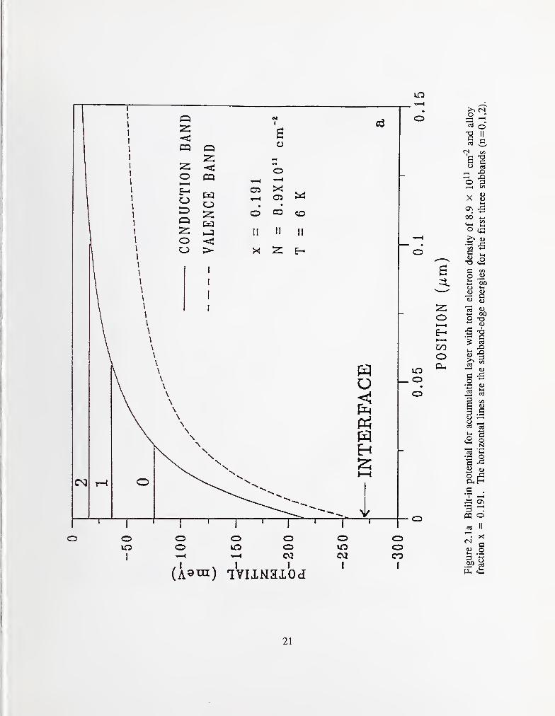
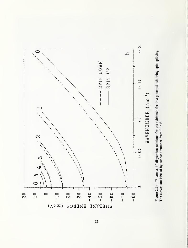
taken to be 6 K, at which the material is degenerate. As an example, the calculated built-in field and
subband dispersion relations for an areal density of 8.9 x 10^^ cm'^ are shown in figures 2.1a and
2.1b, respectively. The surface potential in figure 2.1a is about three times greater than the energy of
the lowest subband edge and over five times the energy gap. The spin splitting is evident in figure
2.1b, and is greatest for the lowest subband. The density of electrons in the spin-up subband is about
15% greater than in the spin-down subband for the lowest four subbands. At the lower densities this
percentage decreases somewhat, especially for the higher subbands, while at higher densities it
remains nearly the same for all subbands. Note also that the deviation from a parabolic to a
nonparabolic, nearly linear dependence of £ on A: is clear for energies only about 10 meV above the
subband edges. The small oscillations in these curves are due to 1% numerical uncertainty in the
solutions.
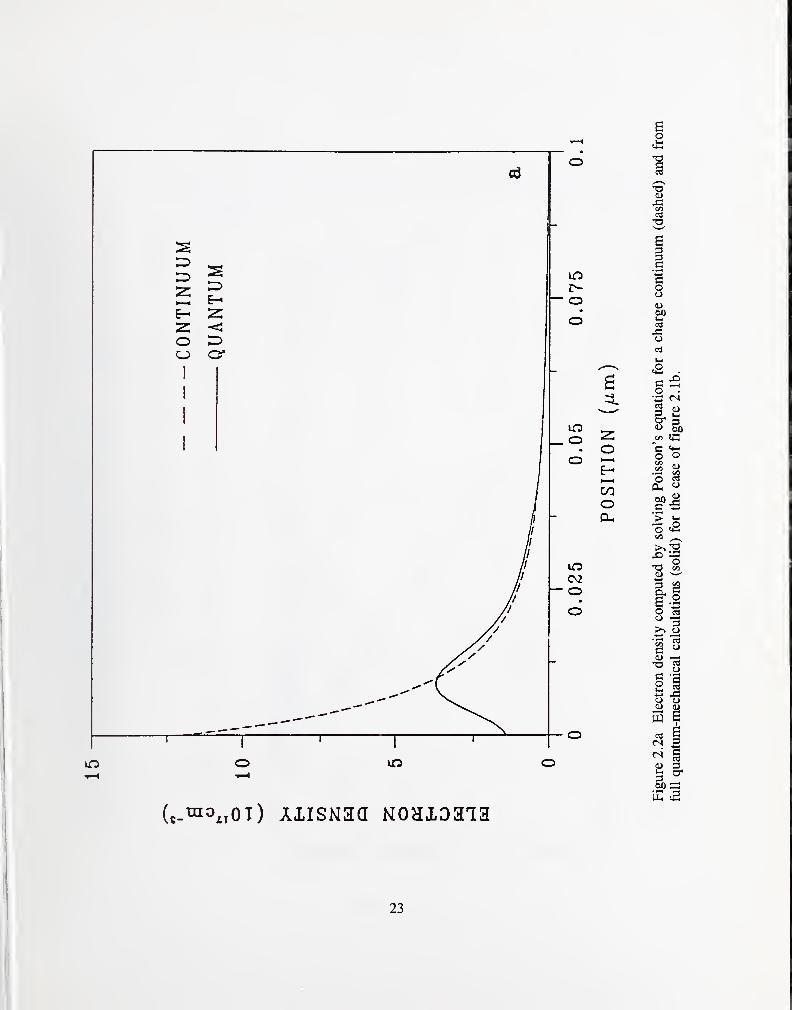
The corresponding electron density in the accumulation layer is shown in figure 2.2a for both the
semi-classical result from the initial solution of Poisson's equation and the final quantum-mechanical
result from the subbands. The width of the accumulation layer is seen to be about 0.1 ixm. The
latter density is greatly reduced at the surface because of the boundary condition on the wave
functions. It goes to zero discontinuously across the boundary because of the dependence of the wave
function on the derivatives offj and /j, which undergo a discontinuous change from a finite to zero
value at the boundary. Therefore, the shape of the potential near the interface is different in the two
cases, and the value of electron density obtained quantum-mechanically is less than that of the initial
semi-classical solution. The electron densities of the first four subbands are plotted as a function of
total density in figure 2.2b. The total density is computed from a sum over only the first four
subbands, for which accurate computations can be performed. The error incurred by this
approximation is estimated to be less than 1 % . The relations are nearly linear with average slopes of
0.673, 0.223, 0.077, and 0.027 for the first (n= 0) through fourth (n= 3) subband, respectively. The
deviations from linearity are less than 1 % . This near linearity shows that the shape of the potential
distribution is relatively insensitive to the magnitude of the surface potential. This linearity has been
observed before experimentally as well, and the values of the experimental slopes are nearly the same
as those calculated [2.1].
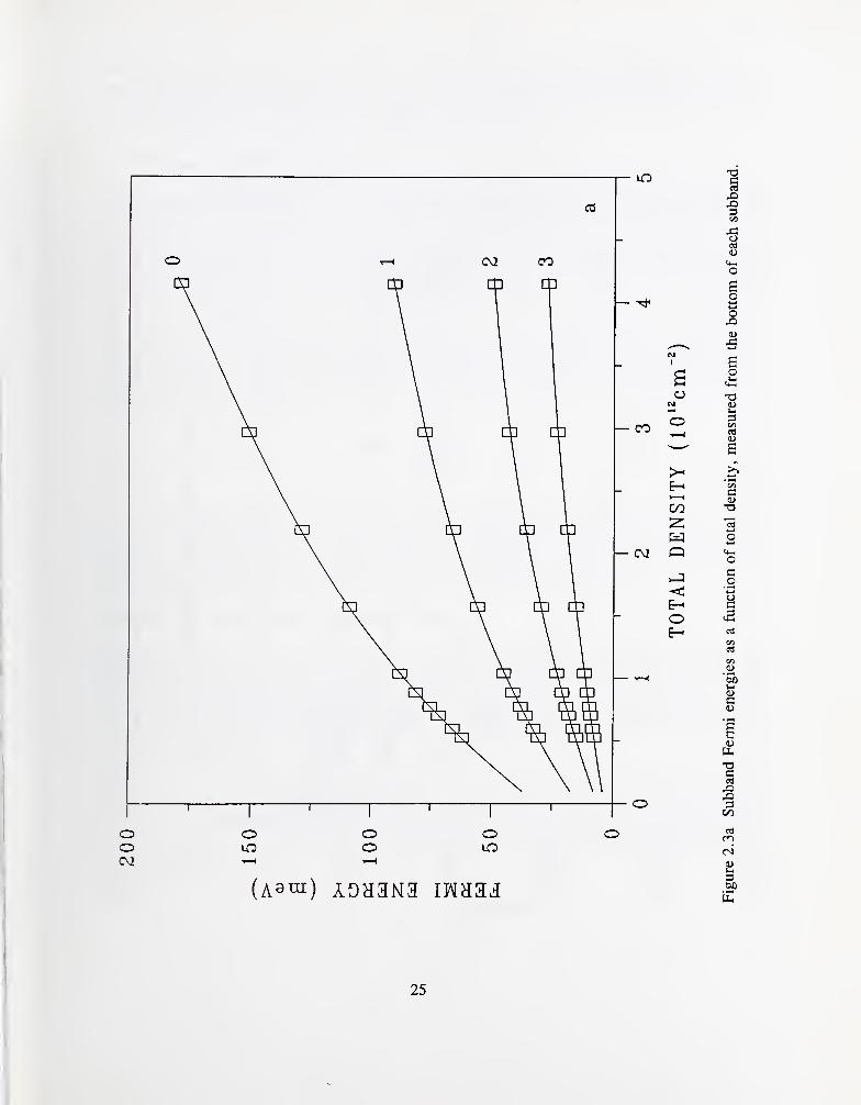
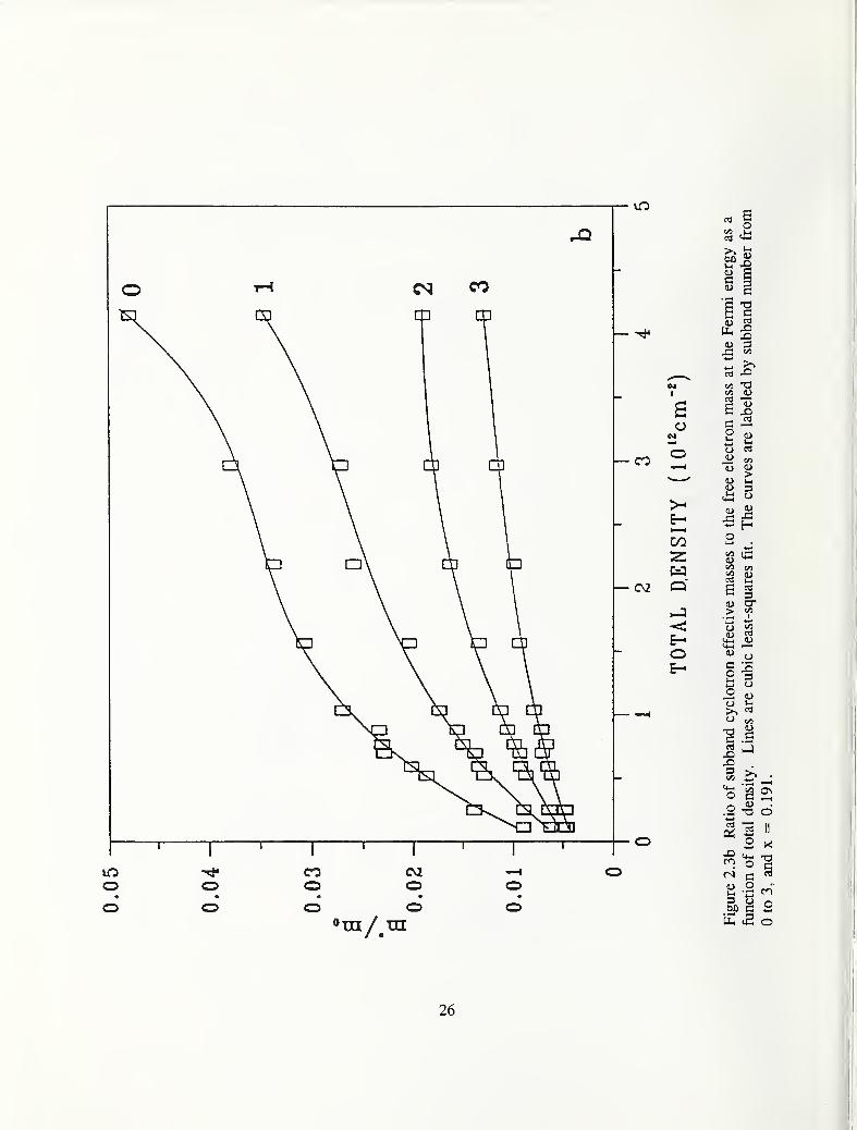
The subband Fermi energies and cyclotron effective masses are shown in figures 2.3a and 2.3b,
respectively, as a function of total density. The Fermi energy in the bulk is computed to be 5.44
meV for an assumed bulk density of 3.9 x 10^^ cm"^. The scatter in the mass values is due to the
derivative in eq (19). Although the calculated eigenvalues appear relatively smooth in figure 2.1b,
they are only accurate to about 1 % , and this uncertainty as well as that due to the discreteness of the
A:-values causes the theoretical masses to have errors of about 5% occasionally. A more refined
calculation would lead to better accuracy. The strong variations of the masses with density attest to
the nonparabolicity of the dispersion relations, which have an effect on the optimization of device
performance. The serpentine shape of the curves is due to the strong curvature of the built-in
potential.
In conclusion, the dispersion relations for the 2D subbands in the accumulation layers of HgCdTedetectors have been computed by solving the 8 x 8 matrix Hamiltonian for a large range of electron
20
C\2
OC\2
OC\2
OCO
OI
o oCO
I
oI
o
LTD
O
OCO
Pi
a;
>
Ml
CO
gO
CO
I
^ 2
^ S
O ^
o ^•Jo
-3"-I S1)
CO X)
= <u
C«
3
.1^
{a9^) ADH3Na QNvaaas
22
23

COa>
COI
'<->
cH
c4
a>i-i
<Uc
XS' ON
c o•a
II
3 X
4—*
ao
c-a
C
3
U
3
-a
(z.xno^jOT) AiisNaa aNvaans
24
o o o oO Irt O iOC\2
25
o o COo CV2o oo
C/5
So
bo a;
c §
X)<u 3
s ^
D (L)
(U ^<i2 o
(U^
52Sen
11
C .5
X .
.2 -So
I I II
tl-l T-l
2 M-Tl-c -^S3 O o£ <S o
26
densities (0.1 to 5 x 10^^ cm"^). The subband densities, Fermi energies, and cyclotron effective
masses have been computed as a function of the total electron density. The results show the effects of
strong nonparabolicity. The near linear dependence of the subband densities on total density, which
has been observed experimentally, has been confirmed theoretically.
(5) Determination of Dingle Temperatiu-es
The oscillations decay with increasing 1/5 (decreasing B) because of the scattering of the electrons by
the lattice, defects, and impurities, which disrupt the cyclotron orbits and broaden the Landau levels.
The term D^(u}^, t^', r^) in eq (1) contains this effect, which is described by the scattering time t/.
This ' differs in value from that of the electron mobility r, because low-angle scattering has a muchsmaller effect on t [2.10,2.11]. However, the scattering mechanisms are the same in both cases, and
the Landau-level broadening can at least be correlated to the mobility.
The values for r^' for each subband are obtained from the decomposed signals S^{B,T^) by dividing
out all the terms in eq (1) except D^{o}^, t^', 0), and plotting the absolute result semilogarithmically,
as demonstrated later. The slope of the line that is tangent to the peaks of the absolute value of the
oscillations gives r^' directly. Another parameter, the Dingle temperature T^,^, is commonly used
instead of t^'. It is defined by:
and is an equivalent measure of the scattering, with high Dingle temperatures implying low
mobilities. The Dingle temperature can only be determined if nearly all the current goes through the
top accumulation layer, which occurs at sufficiently high B-fields, so that the signal amplitude does
not vary because of current division between the accumulation layers and the bulk.
(6) Dependence of SdH Signal on Angle of B-Field
The equations derived in this section are for the 5-field perpendicular to the passivated interface.
This configuration gives cyclotron orbits in the plane of the accumulation layer, which maximizes the
effect of the field on the 2D electron gas. If the angle 6 of the field with respect to the perpendicular
is not zero, then only its component in the perpendicular direction relates to cyclotron orbits. Thus,
all the terms involving B should be replaced with B cos 6, and the peak frequencies/^ all vary as
1/cos d to compensate.
This dependence of the peak frequencies on 6 is a definitive test of whether or not the electrons are
behaving as a 2D electron gas. An example of this is shown later for a GOES detector 2D electron
gas system. In a 3D system, there is no angular dependence because the cyclotron orbits can occur in
any direction. Thus, one can separate 2D and 3D behavior by measuring the angular dependence of
the SdH oscillations.
27
C. Results of Measurements on Specific Detectors
(1) Typical Data
Shubnikov-de Haas oscillations can be recorded with either ac or dc techniques. However, for the
weak oscillatory structure present in most GOES detectors, the much more sensitive ac method which
involves using ac magnetic-field modulation and phase-sensitive detection techniques is chosen for
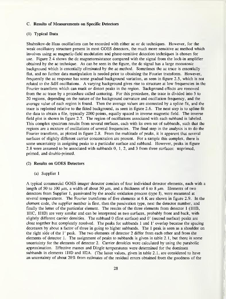
use. Figure 2.4 shows the dc magnetoresistance compared with the signal from the lock-in amplifier
obtained by the ac technique. As can be seen in the figure, the dc signal has a large monotonic
background which is essentially eliminated by the ac method. Sometimes the ac trace is essentially
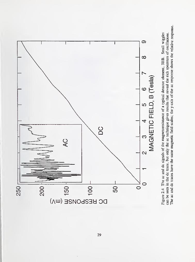
flat, and no further data manipulation is needed prior to obtaining the Fourier transform. However,
frequently the ac response has some gradual background variation, as seen in figure 2.5, which is not
related to the SdH oscillations. A varying background gives rise to structure at low frequencies in the
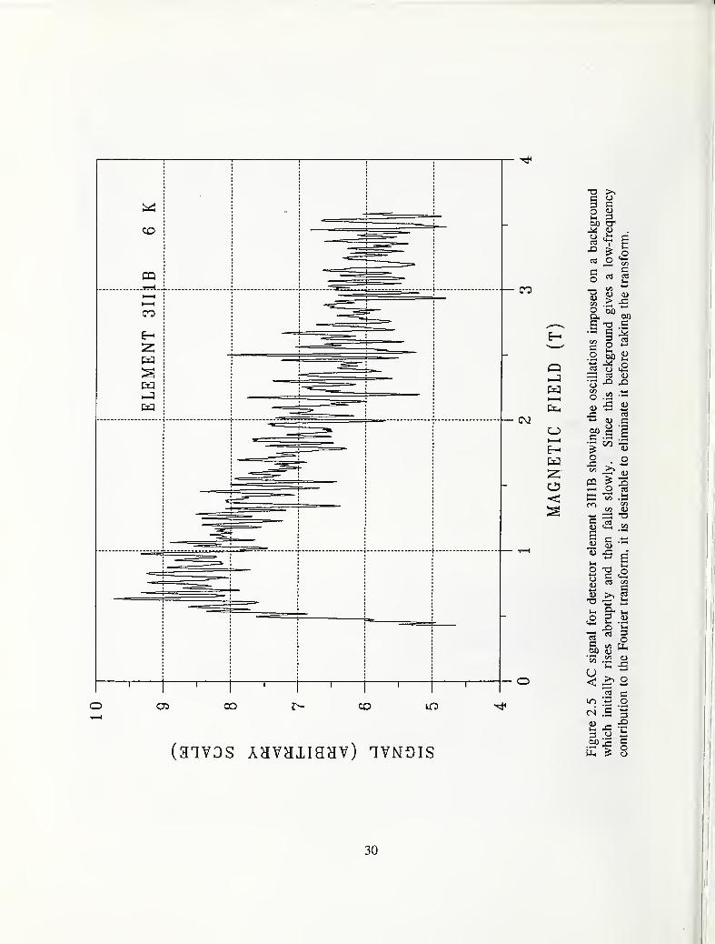
Fourier transform which can mask or distort peaks in the region. Background effects are removed
from the ac trace by a procedure called centering. For this procedure, the trace is divided into 5 to
20 regions, depending on the nature of the background curvature and oscillation frequency, and the
average value of each region is found. Then the average values are connected by a spline fit, and the
trace is replotted relative to the fitted background, as seen in figure 2.6. The next step is to spline fit
the data to obtain a file, typically 2000 points, equally spaced in inverse magnetic field. The inverse
field plot is shown in figure 2.7. The region of oscillations associated with each subband is labeled.
This complex spectrum results from several surfaces, each with its own set of subbands, such that the
regions are a mixture of oscillations of several frequencies. The final step in the analysis is to do the
Fourier transform, as plotted in figure 2.8. From the multitude of peaks, it is apparent that several
surfaces of slightly different carrier concentration are present. For a sample this complex, there is
some uncertainty in assigning peaks to a particular surface and subband. However, peaks in figure
2.8 were assumed to be associated with subbands 0, 1,2, and 3 from three surfaces: unprimed,
primed, and double-primed.
(2) Results on GOES Detectors
(a) Supplier 1
A typical commercial GOES imager detector consists of four individual detector elements, each with a
length of 50 to 100 /xm, a width of about 50 fxm, and a thickness of 6 to 8 /xm. Elements of two
detectors from Supplier 1, passivated by the anodic oxidation process (type I), were measured at
several temperatures. The Fourier transforms of five elements at 6 K are shown in figure 2.9. In the
element code, the supplier number is first, then the passivation type, next the detector number, and
finally the letter of the particular element. The results of the three elements from detector 1 (IIIB,
IIIC, HID) are very similar and can be interpreted as two surfaces, probably front and back, with
slightly different carrier densities. The subband 0 (first surface) and 0' (second surface) peaks are
close together but completely resolved. The peaks for subbands 1 and 1' overlap because the spacing
decreases by about a factor of three in going to higher subbands. The 1 peak is seen as a shoulder on
the right side of the 1' peak. The two elements of detector 2 differ from each other and from the
elements of detector 1. The assignment of peaks to subbands is given in table 2.1, but there is someuncertainty for the elements of detector 2. Carrier densities were calculated by using the parabolic
approximation. Effective masses and Dingle temperatures were determined for the dominant
subbands in elements HID and 112A. (The latter values, given in table 2.1, are considered to have
an uncertainty of about 20% from estimates of the residual errors obtained from the goodness of the
28
(ALU) 3SN0dS3a oa
S ° 2i
moo
o
^ *->
^ <L> n\° ^ ^aj on *->
oC > (/3
S g,^
§3 2 o
S ^ S
-s -s go ^ <u
i2 o §g *o S
^ ^ "S
O (73
fU -t—• -t-j
H .S ^^ s -§
CN on "1) D y
> D
29
31
32
33
aaniiNovH rhojsnvhi namnoi
34
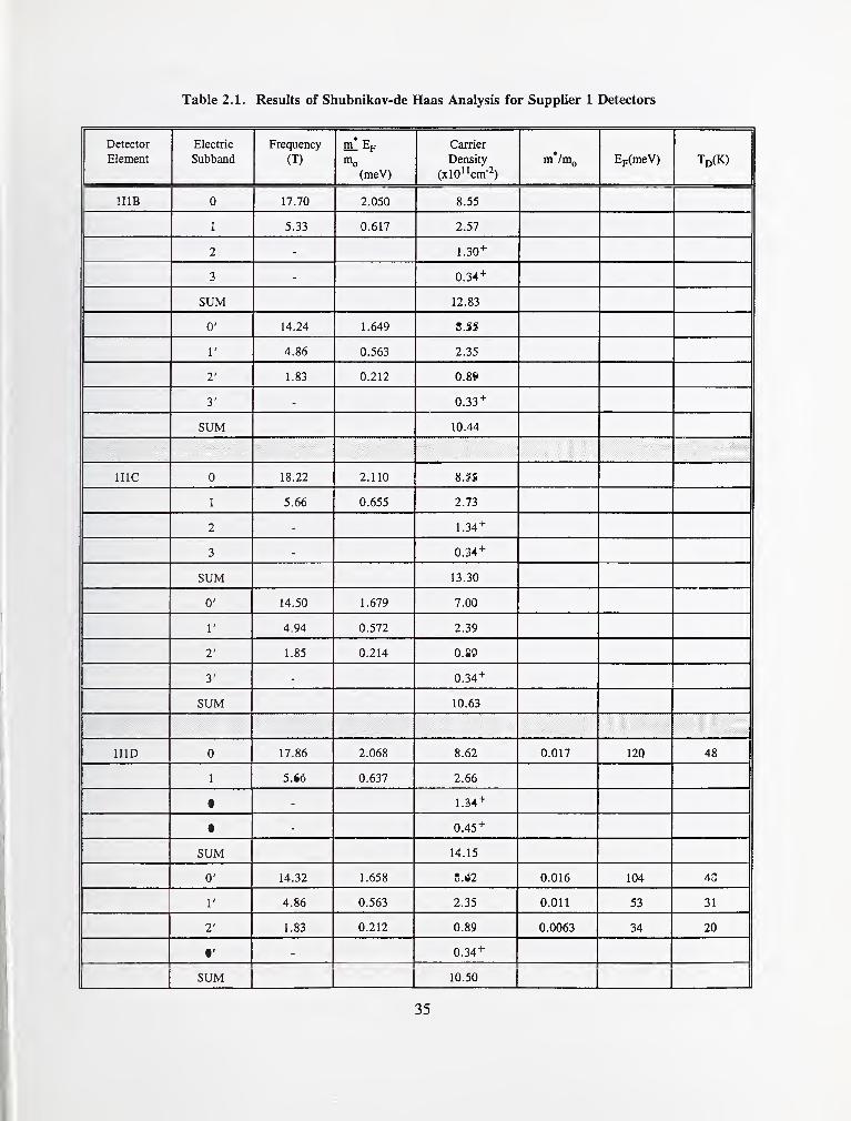
Table 2.1. Results of Shubnikov-de Haas Analysis for Supplier 1 Detectors
Detector Electric
OUL/UailU
Frequency m* Ep
(meV)
Carrier
(xl0"cm-2)
m /nig Cp^inc Y )
IIIB 0 17.70 2.050 8.55
1 5.33 0.617 2.57
2 1.30+
3 - 0.41+
SUM 12.83
0' 14.24 1.649 6.88
1' 4.86 0.563 2.35
2' 1.83 0.212 0.88
3' - 0.33+
SUM 10.44
IIIC 0 18.22 2.110 8.80
1 5.66 0.655 2.73
2 - 1.34+
3 - 0.43 +
SUM 13.30
0' 14.50 1.679 7.00
r 4.94 0.572 2.39
2' 1.85 0.214 0.90
3' 0.34 +
SUM 10.63
HID 0 17.86 2.068 8.62 0.017 120 48
1 5.50 0.637 2.66
2 1.43+
3 _ 0.45 +
SUM 14.15
0' 14.32 1.658 6.92 0.016 104 40
1' 4.86 0.563 2.35 0.011 53 31
2' 1.83 0.212 0.89 0.0063 34 20
3' 0.34 +
SUM 10.50
35
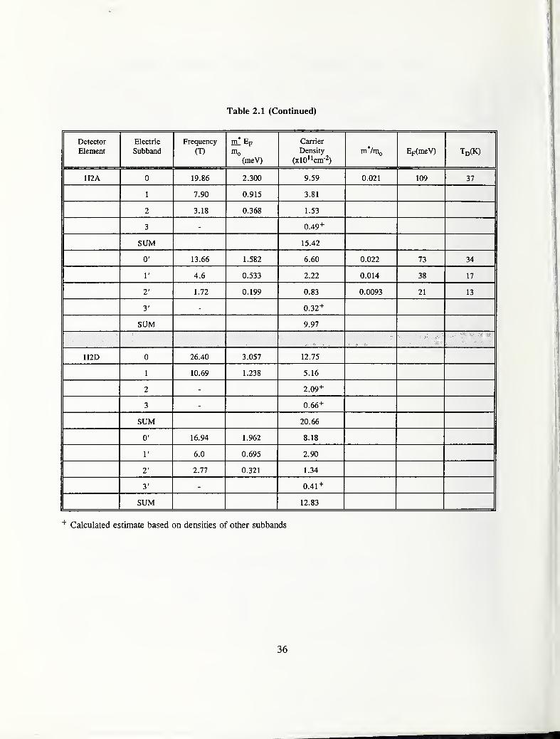
Table 2,1 (Continued)
Detector
Plpni£*nt
Electric
U U L/fl 1 H 1
Frequency
V * /
m Ep
(meV)
Carrier
Density
(xl0"cm-2)
in*/niQ Er^CmeVI
112A 0 19.86 2.300 9.59 0.021 109 37
1 7.90 0.915 3.81
2 3.18 0.368 1.53
3 - 0.49+
SUM 15.42
0' 13.66 1.582 6.60 0.022 73 34
1' 4.6 0.533 2.22 0.014 38 17
2' 1.72 0.199 0.83 0.0093 21 13
3' - 0.32+
SUM 9.97
1I2D 0 26.40 3.057 12.75
1 10.69 1.238 5.16
2 2.09 +
3 0.66 +
SUM 20.66
0' 16.94 1.962 8.18
r 6.0 0.695 2.90
2' 2.77 0.321 1.34
3' 0.41 +
SUM 12.83
Calculated estimate based on densities of other subbands
36

fit.) The subband densities are plotted as a function of total density Nj in figure 2.10. The results of
the linear fits are: Nq = 0.638 N^, = 0.225 N^, and N2 = 0.077 Nj. The subband 3 values
v/ere all calculated by using the relationship N3 = 0.032 Nj Note that the theoretically calculated
values given earlier were 0.673, 0.223, and 0.077, respectively.
(b) Supplier 2
Two detectors of four elements each from Supplier 2 were measured at several temperatures. Theback and front surfaces were passivated by different processes (the combination designated type III),
with the result that the SdH traces are complex and very difficult to analyze. Oscillations associated
with the second process are closely spaced, even at high fields, and continue with the same amplitude
to at least 9 T. Traces at 6 K of the four elements of the first detector are shown in figure 2.11. Thetemperature dependence of element 2III1B is plotted in figure 2.12. The figure shows that the
amplitude of the oscillations decreases with increasing temperature as expected. Traces of the four
elements of detector 2III2 are shown in figure 2.13. The Fourier transforms for detector 2III1 are
plotted in figure 2.14. The identification of peaks associated with particular subbands is difficult. Apossible assignment for element 2III1D is shown on the figure and is given in table 2.2a. TheFourier transforms for detector 21112 are shown in figure 2.15 and are similar to those for detector
2ini. This type of detector is better characterized using the new dc magnetoresistance method
presented in section 4.
To determine if the oscillations were indeed coming from the two-dimensional surfaces, a limited
rotational study was undertaken, as shown in figure 2.16. The magnetic field is perpendicular to the
surface layers at 0° and parallel to them at 90°. The decrease in the response with rotation indicates
that the oscillations are associated with the surfaces rather than the bulk. The residual amplitude at
90° is considered to be the noise level.
In order to better understand the detectors of Supplier 2 with their two different passivations, a series
of three experimental detectors was prepared by Supplier 2 for SdH studies. Detector 2IV5 had the
back surface prepared with the first process passivation, and the front surface was unfinished
(designated by type IV). Detector 216 had both surfaces passivated by the first process, whereas
detector 2III7 had the back surface passivated with the first process and the front surface done with
the second process. The SdH response of these three detectors is shown in figure 2.17. The addition
of the second process is seen to strongly interfere with the oscillations from the first process at low
magnetic fields. The Fourier transforms of these spectra are shown in figure 2.18. The first process
peaks are identified and are similar to those seen in detectors from other suppliers with this type of
passivation. The n=0 subband has three peaks, indicating that the surface has at least three regions
with slightly different carrier densities. The addition of a second surface of the same type gives a
response which is similar to that of one surface with only slight changes in peak frequency and
relative height. The detector with two surfaces passivated, each of a different passivation, has quite a
different behavior. The first process peaks are difficult to identify since they are greatly reduced and
appear to have shifted slightly. The only definite front surface peak (second process) is the one
labeled Is. The Os response is fairly weak and the 2s peak occurs in the region of structure from the
other surface.
Effective masses were determined for four of the subbands of detector 2IV5. The values are in good
agreement with those found for the Supplier 1 detectors which had similar passivation. The
information on carrier density, effective mass, and Dingle temperature is listed in table 2.2b.
37
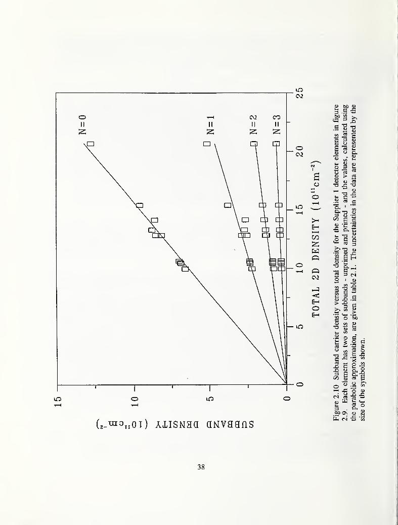
o 1—4 CV2 COII II II II
\cp
Cv2
OCv2
MI
o
o
E-t—
<
m
o
E-O
— lO
in
s .s -s
•S o -a
^ ^ SC 3 (U
5 =1 I-
w c«' ci
fc yO P l-c
o > ^0) 0)J3
--^^!u c
6 J,;3 1) •
—
S .1
O I (U
ill»- 5
go0) CO
COJ3
(^-^^iiOt) AXiSNaa aNvaans
(N CO
>'5b
CO
13 .
O fi
><:^o ^
' o
n g
ca o0)
a N
38

o
oIS
CO 13
1)
Ooo
Si Ma- S
00
X)
4-1 (L>
O-H 3— O
a.
-<U CO-4-^ I—-I
(UT3 C
.2O
11
Vh CO
lis oM-i OO -Z!
CO o
K Si73 O
;-i
COI—
I
(N O<U CO
1/3
tL, O
39

asNOdsan Hoioaxaa ov aAixvian
40
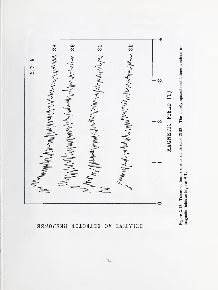
41

42
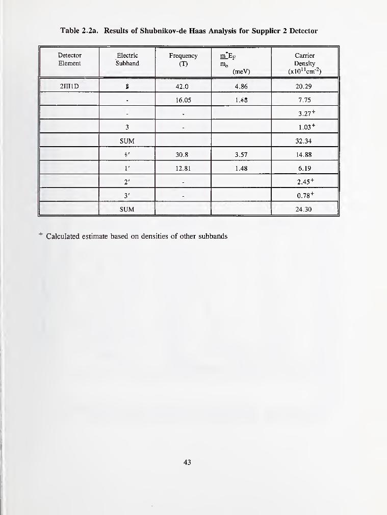
Table 2.2a. Results of Shubnikov-de Haas Analysis for Supplier 2 Detector
Detector
Element
Electric
Subband
Frequency
(T)
m Ep
(meV)
Carrier
Density
(xlOiicm-2)
2111 ID 0 42.0 4.86 20.29
1 16.05 1.86 7.75
2 3.27 +
3 1.03+
SUM 32.34
0' 30.8 3.57 14.88
r 12.81 1.48 6.19
2' 2.45+
3' 0.78 +
SUM 24.30
Calculated estimate based on densities of other subbands
43
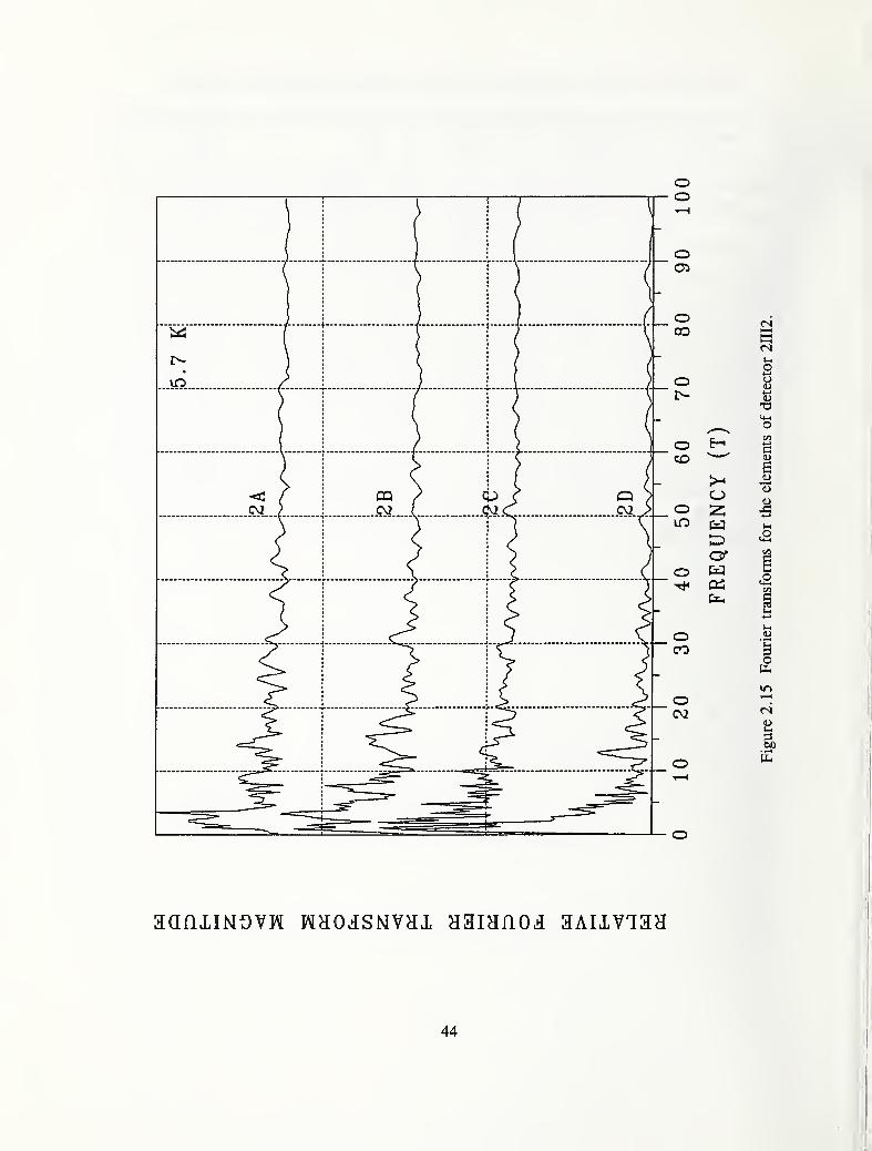
o
44

45
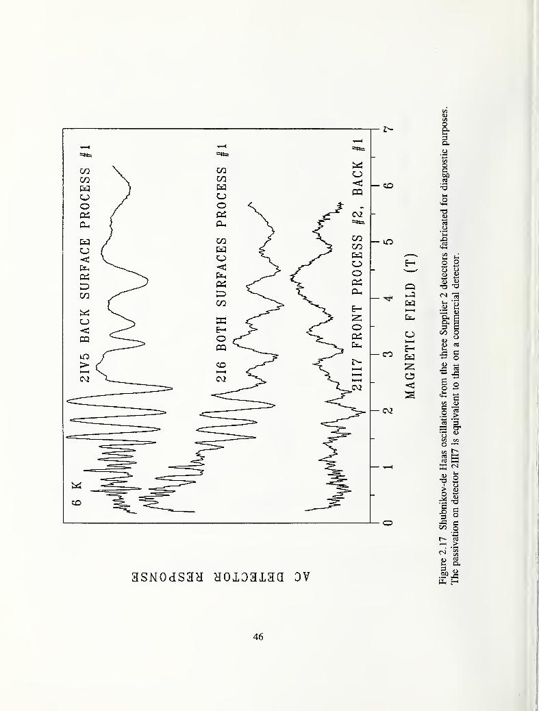
46
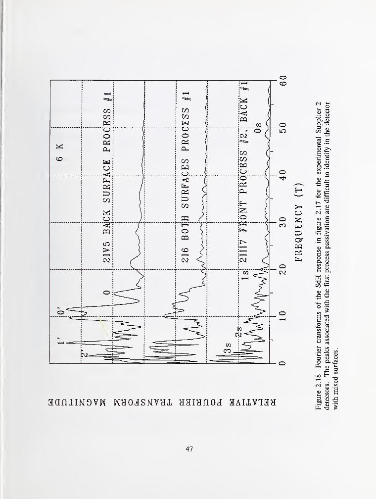
47
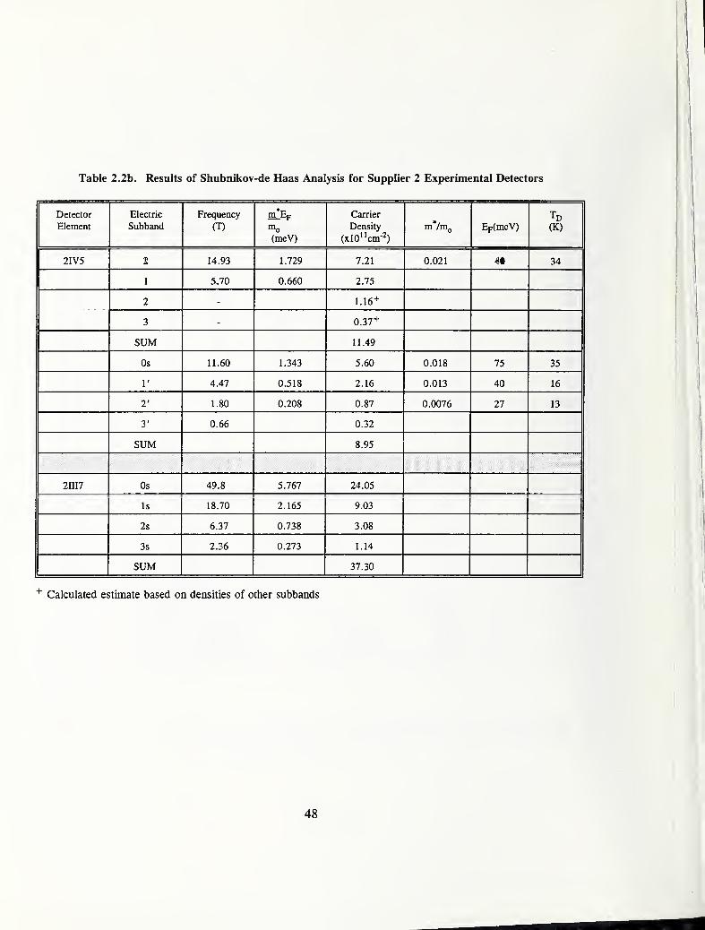
Table 2.2b. Results of Shubnikov-de Haas Analysis for Supplier 2 Experimental Detectors
Detector
Element
Electric
Subband
Frequency
(T)
m_Ep
^0(meV)
Carrier
Density
(xl0**cm-2)
m*/nip Ep(meV) (K)
2IV5 0 14.93 1.729 7.21 0.021 83 34
1 5,70 0.660 2.75
2 - 1.16+
3 - 0.37+
SUM 11.49
0' 11.60 1.343 5.60 0.018 75 35
1' 4.47 0.518 2.16 0.013 40 16
2' 1.80 0.208 0.87 0.0076 27 13
3' 0.66 0.32
SUM 8.95
2III7 Os 49.8 5.767 24.05
Is 18.70 2.165 9.03
2s 6.37 0.738 3.08
3s 2.36 0.273 1.14
SUM 37.30
+ Calculated estimate based on densities of other subbands
48
(c) Supplier 3
Figure 2.19 shows the responses of the two types of Supplier 3 detectors. One element has type I
(anodic oxidation) passivation, whereas the other element has a different, proprietary, passivation
designated here as type II. It is readily apparent that these give very different SdH signatures. The
magnitude of the oscillations is much greater for the type I detectors when recorded at the same
current and instrument settings. The type I element shows the normal SdH behavior in that a series
of oscillations is periodic in inverse magnetic field. For the type II element, the spacing of the
oscillations does not show any obvious pattern due to the complicated, high frequency signal,
although the Fourier transform does show a set of peaks.
The temperature dependence of a type I device, 312A, is shown in figure 2.20. Note that the
oscillations at low magnetic field damp out first with increasing temperature. Figure 2.21 shows the
Fourier transforms of the temperature traces. The transform peaks broaden somewhat with
temperature as evidenced by the decreased resolution of the subband 0 and 0' peaks at 18 K. The
temperature dependence of the peak amplitude can be used to obtain the effective mass as discussed
elsewhere.
Figure 2.22 shows the Fourier transforms from five Supplier 3 type I detector elements. Elements
3I2A through 3I2D were from one detector and 3I3C was from another detector. Elements 3I2A and
3I2B are seen to be essentially identical, 3I2C and 3I2D have a stronger n=0 and n= 1 surface region
with apparent reduction in the other surfaces (denoted by the primes and double primes), and 3I3C
shows a new surface region at the expense of the dominant surface (double-primed subbands) of 3I2A
through 3I2D. The most probable explanation of these Fourier spectra is related to the geometry of
the detector elements. All of the elements have the same active area but the device length, and
consequently the resistance, varies from element to element. Elements 312A and 3I2B have the same
length, 0.0071 cm, and the same Fourier spectra. Element 3I2C is longer, 0.0107 cm, and its
spectrum shows a significant amount of the unprimed surface (subbands 0, 1, and 2). Element 3I2D
is even longer, 0.0132 cm, and has more of the unprimed surface in its spectrum. It appears that the
unprimed surface is the region of the device outside the active area. A coating, or the lack of it, on
the non-active regions produces a surface layer with a different carrier density, which in turn gives
rise to a different Fourier spectrum. The decrease in the peaks of the long elements, compared to the
peaks seen in the short elements, may be due to the effect of series and parallel resistances of the
various layers. Element 3I3C from another detector is equivalent in length to 3I2C. It basically has
the same number of surfaces, but with the strongest one (see for example, the 0" peak) in elements
3I2A through 3I2D essentially absent and one new surface region present. All of the major peaks in
the transforms are listed in table 2.3.
Figure 2.23 shows SdH traces of a Supplier 3 type II detector element at a series of temperatures.
With the many high-frequency oscillations, it is difficult to track a specific oscillation as a function of
temperature. The Fourier transforms for the elements of a type II detector are shown in figure 2.24.
The assignment of peaks to specific subbands is shown for element 3II1B, and given in table 2.4 for
all elements, but the identification is somewhat arbitrary. The unlabeled peaks are associated with
other regions of the surfaces.
Experimental subband carrier densities are plotted versus total density in figure 2.25 for the Supplier
3 type I detector elements listed in table 2.3. The linear fits gave: Nq = 0.656 Nj, Nj = 0.225 N^,
and N2 — 0.087 N^. These compare favorably to the theoretically calculated values given earlier.
49

Q
OI—
H
o
o o
1
c «3 2° «3 o« ?^ t2
C/3 C oDO
1/3 Kl Uo 0)
2 ffi
(U T3
_ 1/3 ^3
4^ CIhJS
<u
(/3
C/2 CI,
CO
.>
>b &( (u
GO —
2 ^ >p
0)
o oSi ^
asNOdsan Hoxoaiaa ov aAUVian
50
51
52
QI—
c
en
O
oo
(U (U
- c
fs -S
O
Q
IZ)
3
OC
^ 5 :t5
-a (L)
(Uooc
6 g« i2
^
- g ^
S J3
3-H :S '
a. o o
o -a>
e
^ m(/I I—
I
o(+5 O
o
tin O
C/2
l-l
l-i
Co
bO (u
B i3
<uocoo
53
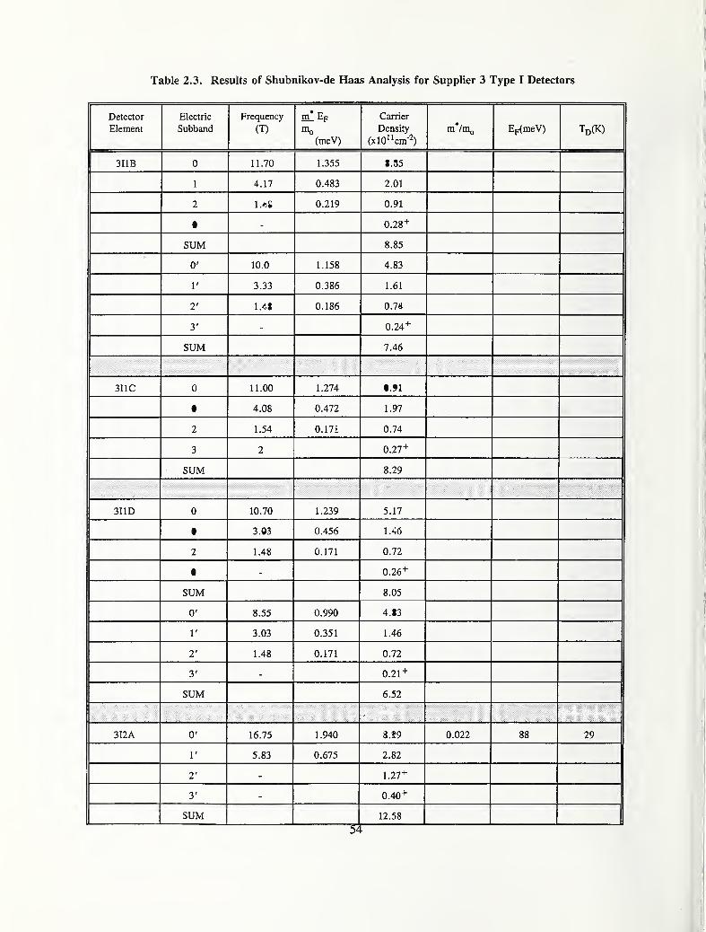
Table 2.3. Results of Shubnikov-de Haas Analysis for Supplier 3 Type I Detectors
Detector
Element
Electric
Subband
Frequency
(T)\ * /
m* Ep
0
(meV)
Carrier
Density
(xlO'lcm-2)
ni*/nig
3I1B 0 11.70 1.355 5.65
1 4.17 0.483 2.01
2 1.89 0.219 0.91
3 - 0.28+
SUM 8.85
0' 10.0 1.158 4.83
1' 3.33 0.386 1.61
2' 1.61 0.186 0.78
3' - 0.24+
SUM 7.46
3I1C 0 11.00 1.274 5.31
1 4.08 0.472 1.97
2 1.54 0.178 0.74
3 - 0.27+
SUM 8.29
3I1D 0 10.70 1.239 5.17
1 3.94 0.456 1.90
2 1.48 0.171 0.72
3 - 0.26+
SUM 8.05
0' 8.55 0.990 4.13
1' 3.03 0.351 1.46
2' 1.48 0.171 0.72
3' - 0.21+
SUM 6.52
-
3I2A 0' 16.75 1.940 8.09 0.022 88 29
1' 5.83 0.675 2.82
2' 1.27+
3' 0.40+
SUM 12.58
54

Table 2.3 (Continued)
Detector Electric Frequency m Ep Carrier
Element Subband (T) Density EpCmeV) Td(K)(meV) (xl0"cm-2)
0" 13.60 1.575 6.57 0.022 72 28
1" 5.05 0.585 2.44 0.014 42 23
2" 2.29 0.265 1.11
3" 0.33 +
SUM 10.45
3I2B 0' 16.60 1.922 8.02
1' 5.5 0.637 2.66
2' 2.20 0.255 1.06
3' 0.39+
SUM 12.13
0" 13.74 1.591 6.64
1" 5.5 0.637 2.66
2" 1.08 +
3" 0.34 +
SUM 10.73
3I2C 0 33.24 3.849 16.05
1 11.35 1.314 5.48
2 3.7 0.428 1.79
3 0.77 +
SUM 24.09
0' 16.23 1.879 7.84
r 5.47 0.633 2.64
2' 2.3 0.26 1.11
3' 0.38+
SUM 11.97
0" 13.54 1.568 6.54
1" 4.58 0.530 2.21
2" 2.1 0.24 1.01
3" 0.32+
SUM 10.08
55

Table 2.3 (Continued)
Detector
Element
Electric
Subband
Frequency
(T)
m Ep
mo(meV)
Carrier
Density
Will t
ni*/m(j EF(meV) Td(K)
u jz.z J. /zy 1 J.JJ
i iU. /J 17/1^ < 1 Q
z i.jy n /1 1
A
U.'f 10 1 71
J f\ 7/1 +U. /4
oUM 7*2 7 1
(J lo.j 1 nil1 .yl 1
7 n77.97
1 j.oU n /;77U.O/Z z.oO
Z 1 7C +l.ZD
3' 0.40+
SUM 12.42
0" 12.81 1.483 6.19
1
"
4.85 0.562 2.34
2" 2.15 0.249 1.04
3" 0.32 +
SUM 9.89
3I3C 0 33.27 3.853 16.07
1 10.75 1 .245 5.19
2 3.85 0.446 1.86
3 0.76+
SUM 23.88
0' 25.75 2.982 12.44
r 8.87 1.027 4.28
2' 3.55 0.411 1.71
J U.Ol
SUM 19.04
0" 16.4 1.899 7.92
1" 5.88 0.681 2.84
2" 2.52 0.292 1.22
3" 0.40+
SUM 12.38
Calculated estimate based on densities of other subbands
56
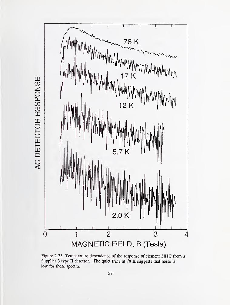
1 II I I I I U I I
0 12 3 4
MAGNETIC FIELD, B (Tesia)
Figure 2.23 Temperature dependence of the response of element 311IC from a
Supplier 3 type II detector. The quiet trace at 78 K suggests that noise is
low for these spectra.
57

58

Table 2.4. Results of Shubnikov-de Haas Analysis for Supplier 3 Type II Detectors
Detector
HiClUCIlL
Electric
OUUUdXlU
Frequency m Ep
(meV)
Carrier
Density
(xlO^'cm-^)
m /hIq n.p(,me V j
3111/^ 0 192.6 22.30 93.03
1 65.1 7.54 31.44
2 22.0 2.55 10.63
3 7.0 0.81 3.38
SUM 138.48
0' 128.9 14.93 62.26
r 43.0 4.98 20.77
2' 13.4 1.55 6.47
3' 5.2 0.60 2.51
SUM 92.01
0" 95.4 11.05 46.08
1" 32.0 3.71 15.46
2" 9.8 1.13 4.73
3" 3.5 0.41 1.69
SUM 67.96
3II1B 0 144.0 16.68 69.55
1 53.9 6.24 26.03 0.015 416
2 20.4 2.36 9.85
3 7.2 0.83 3.48 0.0081 102
SUM 108.91
0' 115.6 13.39 55.83
r 44.2 5.12 21.35
2' 16.0 1.85 7.73
3' 5.4 0.63 2.61
SUM 87.52
0" 84.8 9.82 40.96 0.023 427
1" 28.4 3.29 13.72
2" 11.0 1.27 5.31
3" 4.1 0.47 1.98
SUM 61.97
59
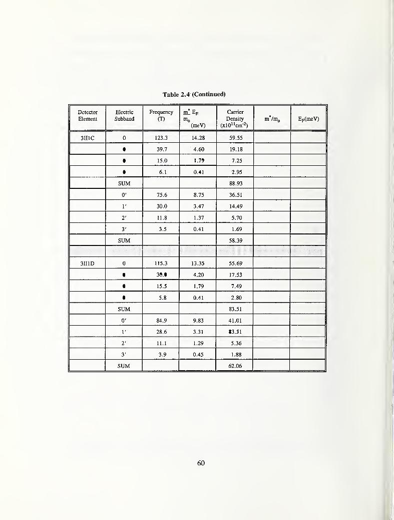
Table 2.4 (Continued)
Detector
Element
Electric
buDband
Frequency
(1)
m Ep
nig
(meV)
Carrier
Density
(xl0"cm-2)
bp(meV)
3II1C 0 123.3 14.28 59.55
1 39.7 4.60 19.18
2 15.0 1.74 7.25
3 6.1 0.71 2.95
SUM 88.93
0' 75.6 8.75 36.51
1' 30.0 3.47 14.49
2' 11.8 1.37 5.70
3' 3.5 0.41 1.69
SUM 58.39
3II1D 0 115.3 13.35 55.69
1 36.3 4.20 17.53
2 15.5 1.79 7.49
3 5.8 0.61 2.80
SUM 83.51
0' 84.9 9.83 41.01
1' 28.6 3.31 13.81
2' 11.1 1.29 5.36
3' 3.9 0.45 1.88
SUM 62.06
60

61
0.673, 0.223, and 0.077, respectively. All of the subband 3 values were calculated using N3 =0.032 Nj. Figure 2.26 is a subband carrier density plot for the Supplier 2 type III and Supplier 3
type II detector elements given in tables 2.2 and 2.4, respectively. The subbands identified for the
Supplier 2 element are considered to be associated with the second passivation process, and the
Supplier 3 type II elements had the same alternate passivation on both sides. The results of the linear
fits are: Nq = 0.660 N^, Nj = 0.229 N^, N2 = 0.083 N^, and N3 = 0.029 N^. Once again, these
are in excellent agreement with the theoretically calculated values.
Figure 2.27 shows SdH data for the rotation of element 312A from a type I detector with respect to
the magnetic field direction. At 0° the field is perpendicular to the accumulation layers, whereas at
90° it is in the plane of the layers. The disappearance of the oscillations with rotation shows that the
SdH effect is coming from the two-dimensional layers rather than the bulk. Particular peaks in the
waveform are seen to be at higher fields at 30° than at 0°. The quantization depends on the
component of the field in the direction of the layer thickness. Thus, the peak position varies as the
cosine of the angle. This can be seen best in figure 2.28 which shows the Fourier transforms of the
data at the four angles. The identified peaks are seen to shift to higher frequency with increasing
angle as predicted. The rotation is seen to be useful in resolving double peaks. - The 1' peak is not
clearly resolved in the 0° transform, but the 60° transform shows distinct 1 and 1' components. The
rotation also confirms that the subband 0 peak has two components. Figure 2.29 is a plot of the peak
positions, normalized to the 0° value, as a function of the rotation angle. The expected cos 6
dependence is shown, and the agreement is considered reasonable in that the rotation was
accomplished by wedges rather than a precision mechanism.
It is instructive to see how well the major peaks in the Fourier transform describe the original SdHdata. To do this, an inverse transform of each peak is obtained and the results summed. Somedistortion is introduced because the peaks are truncated on each side. Inverse transforms were done
for the peaks identified as subbands 0', 0", 1", 2", and harmonic 1" for element 312A in figure
2.21. The waveforms are shown in figure 2.30 along with their sum and the original data. The
synthesized spectrum is seen to be a good reproduction of the original. This same reconstruction was
done for the more complicated data of element 3II1B from figure 2.24. As shown in figure 2.31,
inverse transforms of 12 Fourier peaks were combined and compared with the data. The sum is a
reasonable representation of the data, especially at higher values of inverse magnetic field because a
greater percentage of the Fourier peak area was identified and transformed at lower frequencies. It is
useful to sum the identified components to see if the signal is well represented by them.
(3) Results on TIROS Detectors
Figure 2.32 shows the SdH traces for six different TIROS detectors. These are large, single-element
devices, about 170 ixm by 170 ixm. The TIROS detectors of figure 2.32 varied in resistance by a
factor of five and the detector current for the measurements was adjusted accordingly. Although
similar type SdH oscillations are observed for all the devices, there are reproducible differences which
demonstrates that each SdH trace is a unique signature for an individual detector.
The Fourier transforms of the six detectors in figure 2.32 are shown in figure 2.33. They can be
categorized into two groups of three detectors each, based on the position of the 1 and 1' subbands.
The groups were received at different times which suggests that they were chosen from lots with
somewhat different material characteristics or surface passivation. The subband 0 response for
detector T60367 is composed of three or four peaks, which suggests a corresponding number of
62

(s-^^ziOt) AiiSNaa QNvaans
O <UI—> x*
•a X
I-
.a c
.2 H
a,
1/3•a
(N 2i
.ii £
X! !^
a 8
«3
53 != ^T-l I—
I
CI,
»
1)
o ?
2 c d
•r o
^.52 •£
o ^gj O
^ ''J
S ri
^ -a
S3^
OS 2
60 !D
03 (U
C
ID
a,
O „
(U G.t=! ^ t;
5i S a
63
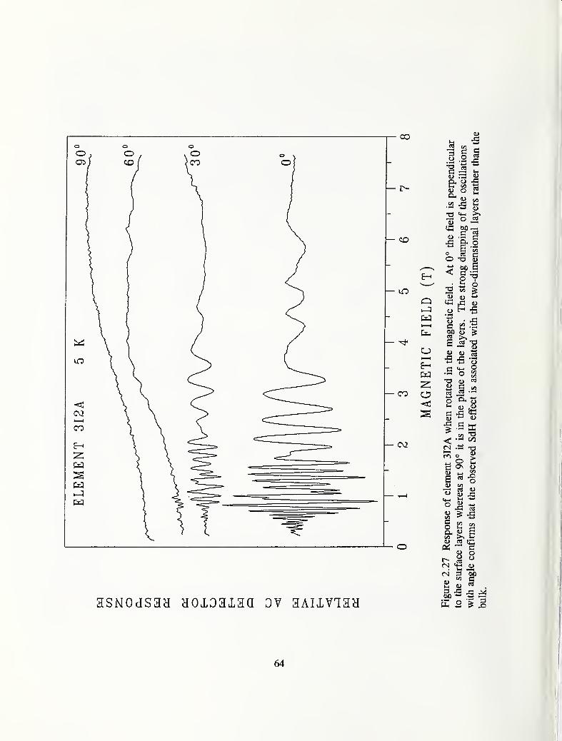
64
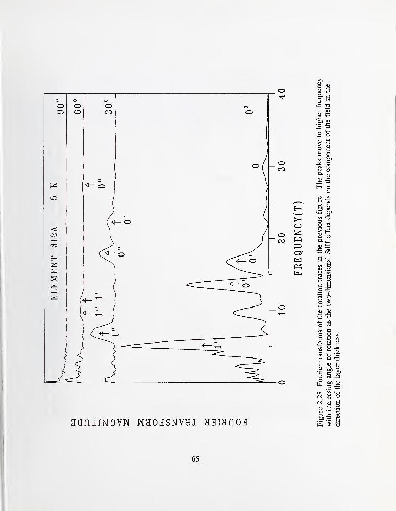
65
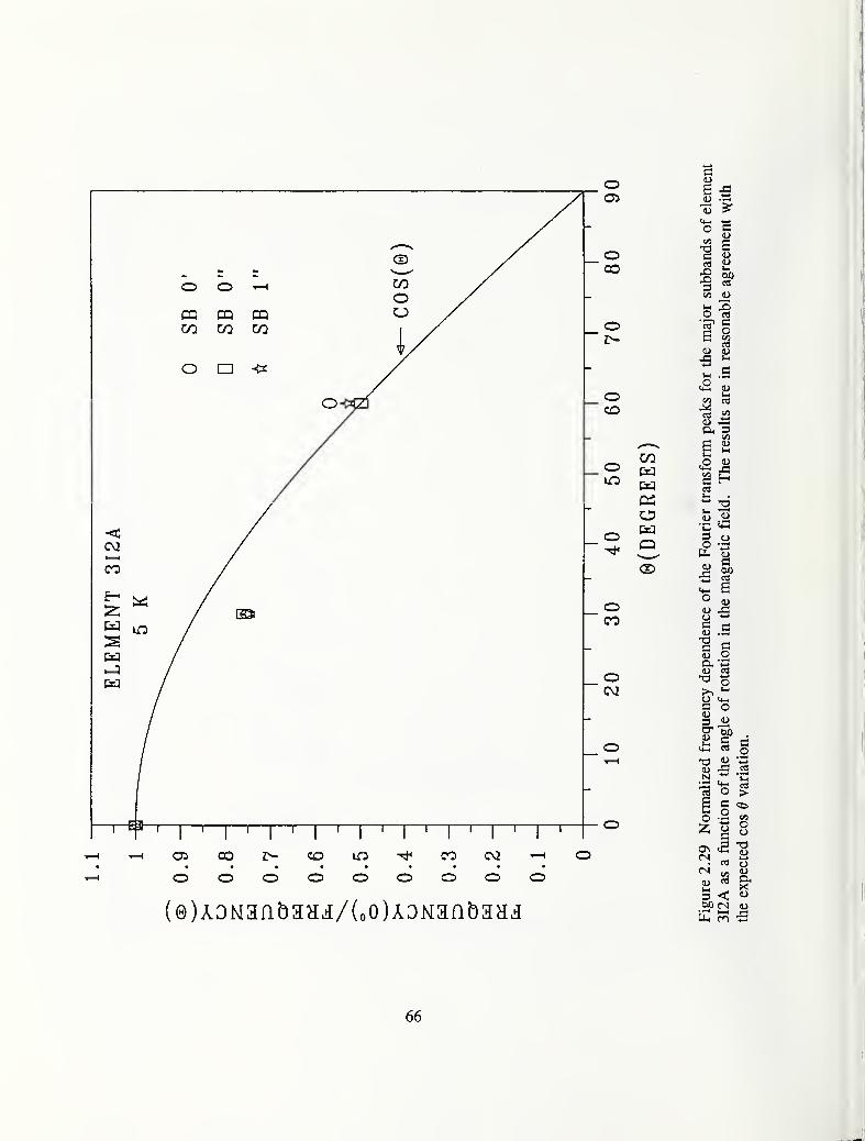
66
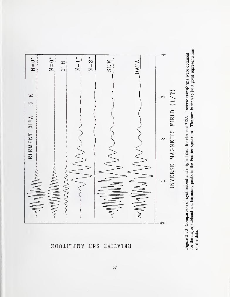
67
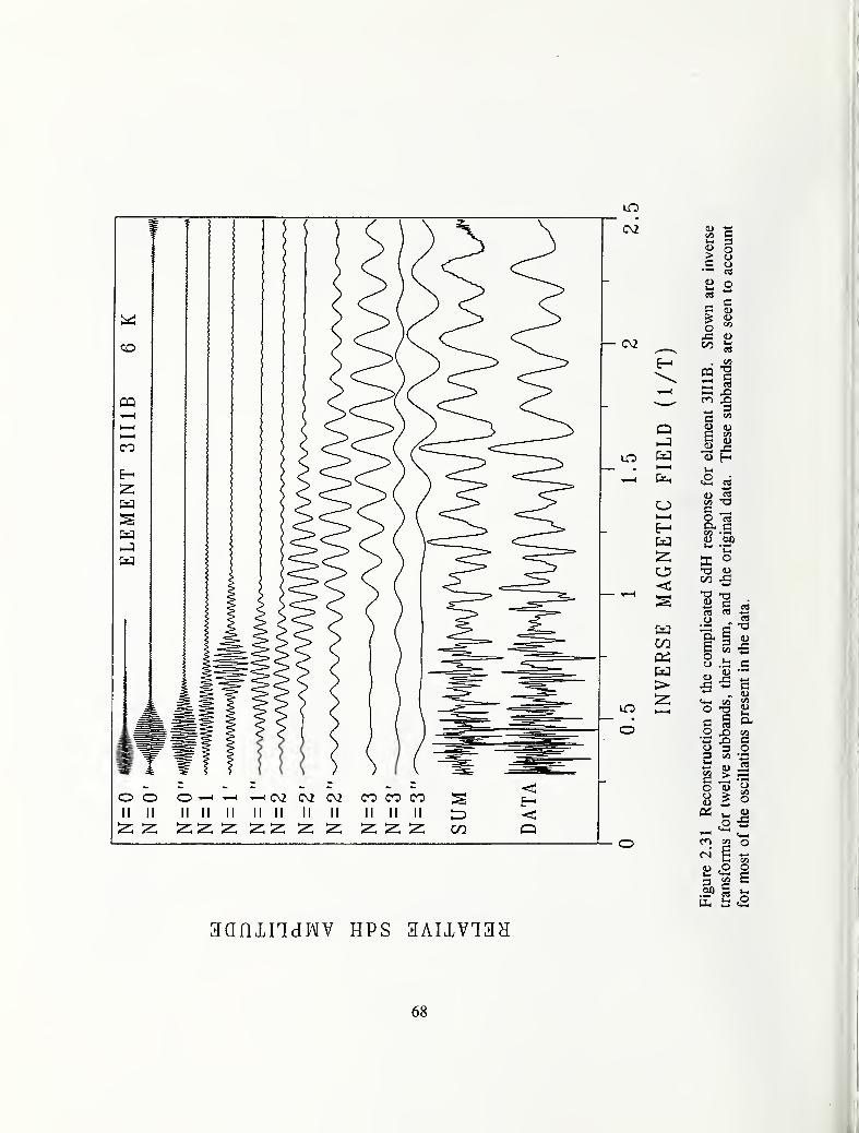
aanxndwv hps aAiivian
68

asN0dS3H Hoxoaiaa ov aAUvian
69
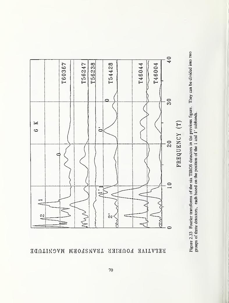
70

partial surfaces with slightly different electron densities. The composite nature gives rise to shoulders
in the subband 1 peak. Detectors T46044 and T46004 were fabricated from the same wafer and have
the most similar Fourier transforms, but reproducible differences are still seen. The parameters
calculated from the subband peak positions are given in table 2.5.
Figure 2.34 shows the SdH traces for detector T56238 at five temperatures. Evidence of the largest
oscillations is seen even at 28 K. The Fourier transforms of these traces are plotted in figure 2.35.
The major subband peaks are identified and the frequency positions and calculated parameters are
listed in table 2.5. Subband density is plotted versus total density for the TIROS detectors in figure
2.36. Linear fits gave the following relationships good to better than 1%: Nq = 0.667 Nj, Nj =
0.220 N^, and N2 = 0.083 N^, in excellent agreement with the theoretically calculated values. All of
the subband 3 densities, except one, were calculated using N3 = 0.032 Nj.
Effective masses for the various subbands were obtained from fits of the inverse transform amplitude
as a function of temperamre as discussed in an earlier section. Specifically, the logarithms of the
amplitudes are fit to the theoretical variation ln{Tsinh {^Tjn /m^)/T^inh (^Tm /m^)] by choosing
m to give the best nonlinear least-squares fit. T^ is the reference temperature, usually the lowest
temperature, and (3 = lirkgmjefi = 14.68 T/K. The use of the logarithmic dependence produces a
more accurate fit because the small signal values at higher temperature contribute more than they
would in a linear plot. The fit for the mass of subband 0' for detector T56238 is shown in figure
2.37. The masses obtained for the other subbands of this detector are given in table 2.5.
Dingle temperatures were calculated for the subbands of detector T56238; the values are listed in
table 2.5. The procedure is to obtain the inverse transform of the Fourier transform peak for the
subband of interest. The inverse signal is divided by all terms except that containing the Dingle
temperature. The log of the absolute value of this quantity is plotted as a function of 1/B and the
Dingle temperature is calculated from the slope of the line that is tangent to the peaks in the region
where the inverse transform is strongest. The plot for subband 0' is shown in figure 2.38.
(4) Intercomparisons
An SdH trace from each group of detectors is shown in figure 2.39. The responses from devices
fabricated with alternate passivation, 2III1D and 311 IB, have a noisy look, and are much lower in
magnitude than the responses from the devices with the standard anodic oxide. When calculating the
scale factors, no allowance was made for differences in magnetic field modulation, current, or goes
here resistivity. The Fourier transforms of these traces are shown in figure 2.40. Again, the
amplitude of the devices with alternate passivation is much less than that of the other devices. Even
though the anodic oxide devices all have basically the same set of subband peaks, there are still
significant differences. The devices with alternate passivation have a carrier density about 3 to 10
times higher than those with anodic oxidation passivation. The responsivity of the alternate devices
reported by the manufacturers is also much higher.
Dingle temperatures could not be reliably extracted for the nonanodically oxidized surfaces.
However, the Dingle temperatures are in general agreement from device to device for the anodically
oxidized surfaces except that element 3I2A has lower temperatures for the 0 subbands than the rest of
the devices. The theory predicts, and NIST results confirm, a systematic decrease in the Dingle
temperature in going from subband 0 to subband 3. As discussed in a previous section, this is
because the electrons in the lower subbands are closer to the surface, with its lower mobility, than the
71
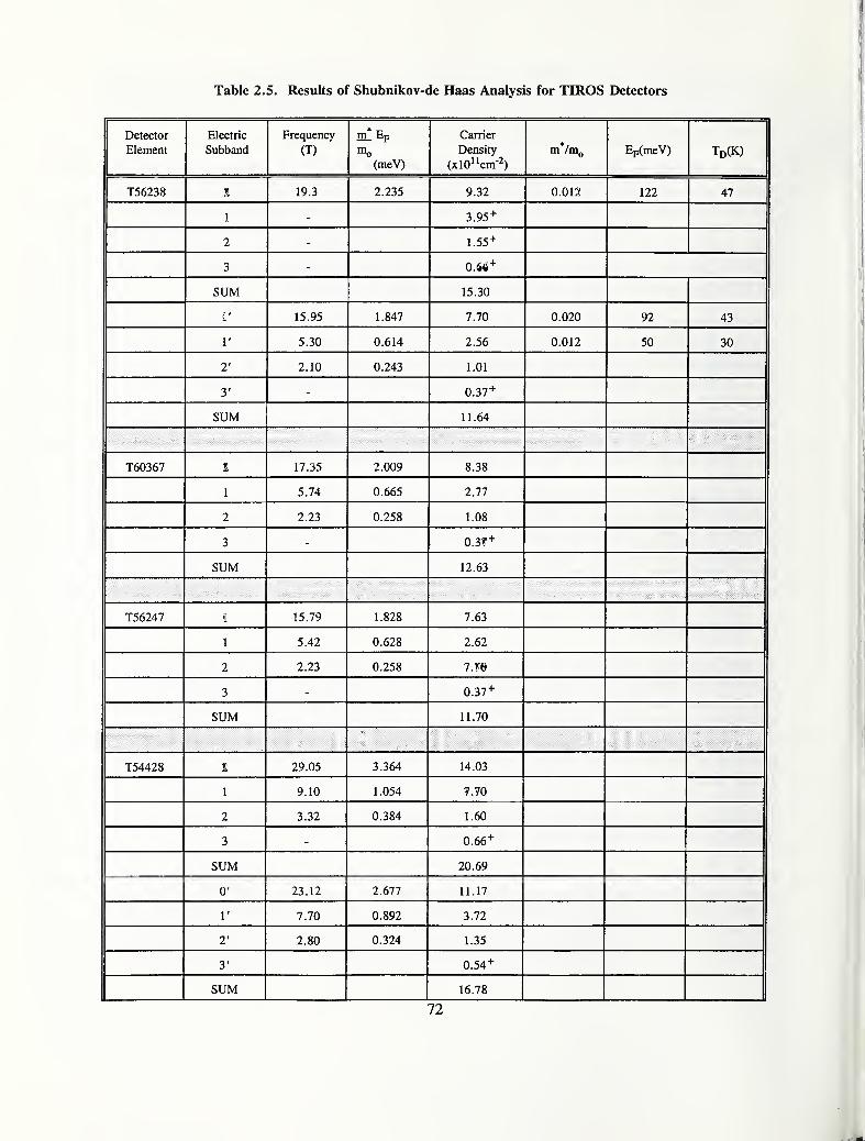
Table 2.5. Results of Shubnikov-de Haas Analysis for TIROS Detectors
Detector Electric Frequency m Ep Carrier
Element Subband (T) Density EF(meV) Td(K)(meV) (xl0"cm-2)
T56238 0 19.3 2.235 9.32 0.018 122 47
1- 3.95+
2 - 1.55+
3 - 0.49+
SUM 15.30
0' 15.95 1.847 7.70 0.020 92 43
1' 5.30 0.614 2.56 0.012 50 30
2' 2.10 0.243 1.01
3' - 0.37 +
SUM 11.64
T60367 0 17.35 2.009 8.38
1 5.74 0.665 2.77
2 2.23 0.258 1.08
3 - 0.40+
SUM 12.63
T56247 0 15.79 1.828 7.63
1 5.42 0.628 2.62
2 2.23 0.258 1.08
3 - 0.37+
SUM 11.70
T54428 0 29.05 3.364 14.03
1 9.10 1.054 4.40
2 3.32 0.384 1.60
3 - 0.66+
SUM 20.69
0' 23.12 2.677 11.17
1' 7.70 0.892 3.72
2' 2.80 0.324 1.35
3' 0.54+
SUM 16.78
72
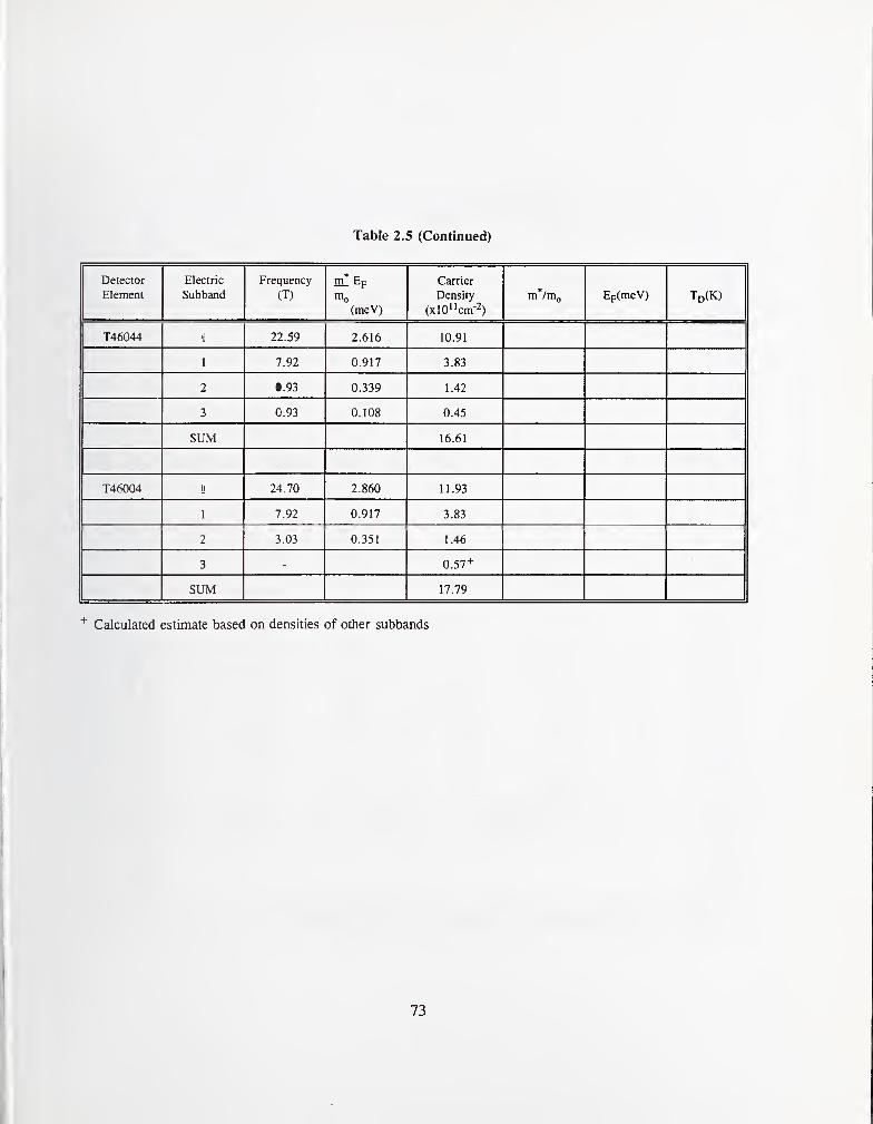
Table 2.5 (Continued)
Detector
Element
Electric
Subband
Frequency
(T)
m Ep
nig
(meV)
Carrier
Density
(xlO"cm"2)
Ep(meV) Td(K)
T46044 0 22.59 2.616 10.91
1 7.92 0.917 3.83
2 2.93 0.339 1.42
3 0.93 0.108 0.45
SUM 16.61
T46004 0 24.70 2.860 11.93
1 7.92 0.917 3.83
2 3.03 0.351 1.46
3 0.57 +
SUM 17.79
Calculated estimate based on densities of other subbands
73
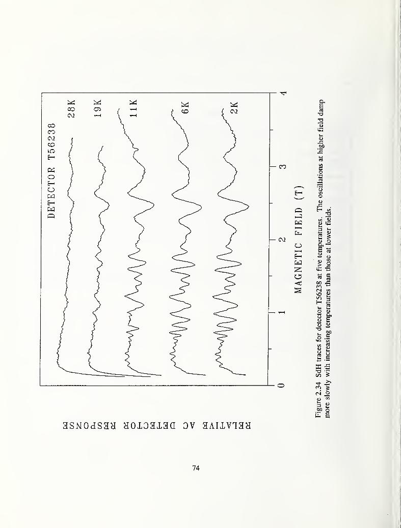
asNOdssH HOJLoaxaa ov aAuvTan
74
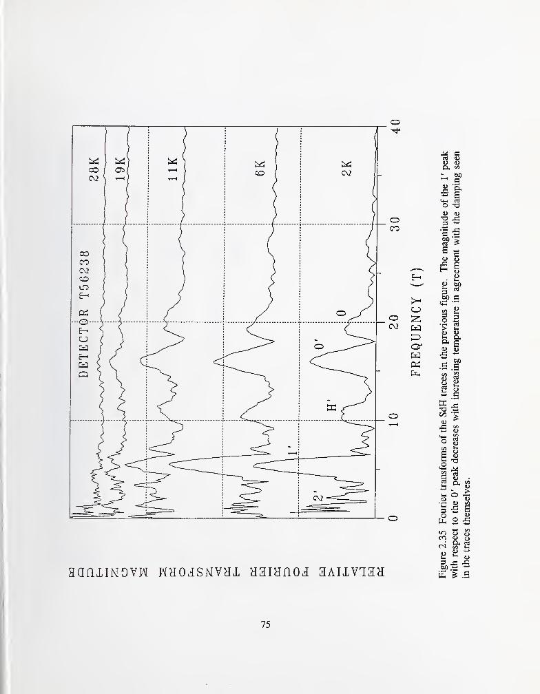
IS
^ C3
(U (U
O 73lU (U
•s^
6 «0) D
i-iU (50
00 c
.2 §> >-
^ s
1/3
J3 ?5
Uo
<U
>a3
3o
<L)
6
<^ (L) o
(u 2iS '-' D00^ ^£ ^ .s
75
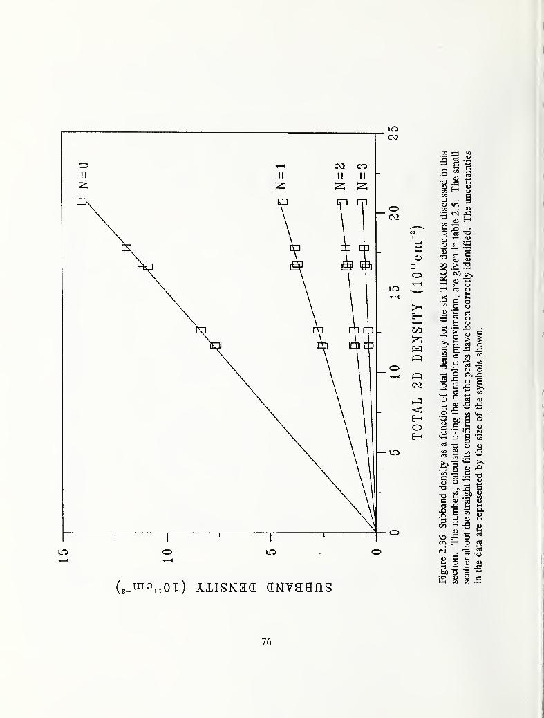
o
I—
I
CO
QQCN2
•-3
OE-
in
2 -Si
COI/}
— : 0)<N Si
o "rt -a
^ r: ^(U
OPiI—
I
HCO o
>-i .is
o
T3
O *-> M
ooa
(U 5>; ^2 oCO «3
COcz<U OP- ^?a S^ CO
(UN
(2-rao„oT) AxisNaa QNvaans
«->CO —
2
(U o-a
en E-i
ci .
Mh CO
oCO
^ (U
•-I is
o <fl
CO -S
76
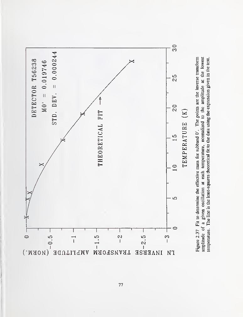
77
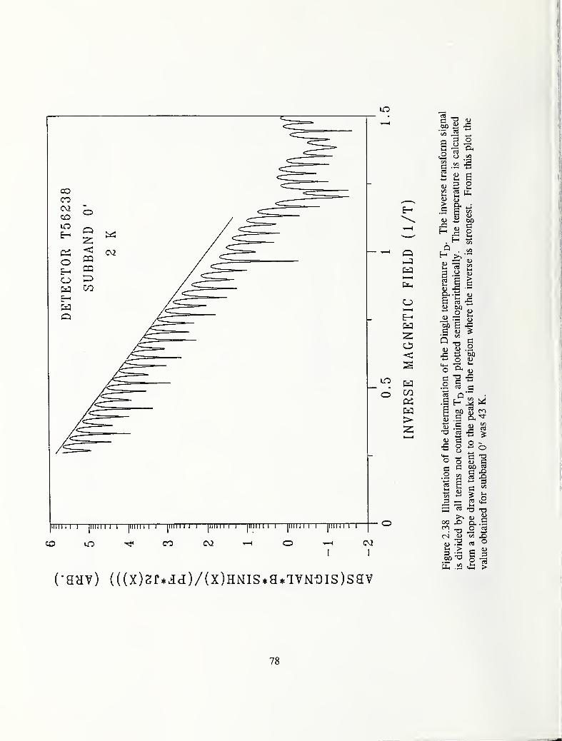
Ill 1 1 I
—
[
ll llll I I
—[
l ll ll l I I—lllllll I I—llllll 1 1 I—llllll 1 1 I—llllll 1 1 I—llllll 1
1
I I
(•anv) (((x)2f*id[)/(x)HMis*a*7VNois)sav
-5 «
2 i! Su 3 21) D> a,.S S
.~
c/3
i-i
3 .a SS ^
»-i S C3
6 S -S
O ^
C <U ^Q ^ c
o
.2 ^X3
o o
.2
2 b
3 —
.
OO X3
00 ^in .22
t-l
Cl, .5O
-t—
•
6 0)
2
78
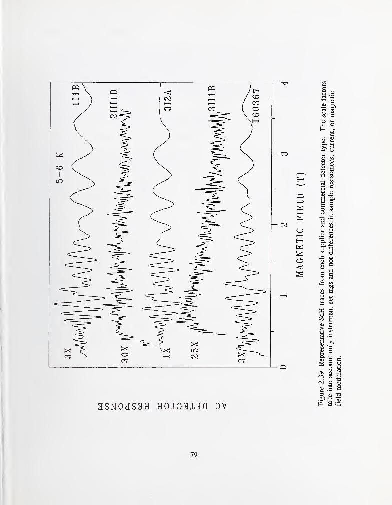
79
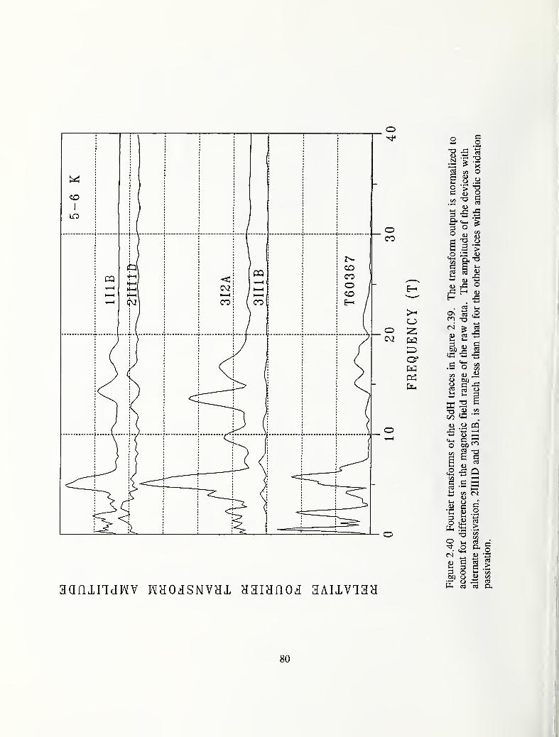
o
oCO
o IS
W
o-a<U
73<u0
noi evi
1/5
(L>3D.3 00 U
T33
sfoi iplil
C3ai-i•4-^
(i>
<uJ3HOn
-t—
»
rn
fNa>
i-i
figu(U
,g
Uca a
PS fie
oe
J3
J3
i
O W)
T—
(
S I—
I
c
i3 !>; <s
3
-a
2 ^
is =33 O00 o
0)o<u _
03>
CIo
>C(U (/I
80
electrons in the higher subbands.
The values of the Dingle temperature were quite large compared with the values around 3 K which
were computed on the basis of the measured mobility. Theoretical calculations [2.11] have shownthat the Dingle temperatures can be much larger than those derived from the conductivity mobility
because the relaxation time affecting the Dingle temperature is much more sensitive to forward
scattering. For Coulomb repulsion due to surface-charge scattering, it is expected that the Dingle
temperatures should be as large as measured. Thus, it is concluded that the behavior of the
anodic-oxide passivation is well understood.
D. Summary of Quantmn Magnetotransport Characterization Measwements
(1) Comparison between Theory and Experiment for Two Different Detector Types
Shubnikov-de Haas measurements have been made on a number of long-wavelength, commercial,
n-type PC detectors with total densities between 5 x 10^^ and 1 x 10 cm"^. The SdH Fourier
transforms of two different representative detectors are shown in figures 2.41a and 2.41b. The
notations ' and " refer to different surfaces or to different regions on the same surface, since both
surfaces of the detector were passivated. The detector in figure 2.41a was passivated with the usual
anodic oxidation process [2.12,2.13], while that in figure 2.41b was passivated by a different method.
The separations of peaks due to spin-splitting as predicted by theory are about half of that observed,
and, thus, it is expected that these multiple peaks are due to different surface densities. The splittings
vary somewhat from detector to detector as well. Thus, the effect of spin-splitting is just to broaden
each peak. The transform corresponding to the detector with lower total density, element 312A in
figure 2.41a, has clear, strong peaks, while that for the one with higher density, element 3II1B in
figure 2.41b, has peaks that rise less above the background. One reason is that the penetration of the
energy gap by the wave functions is much greater for the heavily accumulated case, especially for the
lowest subband. There is a mixture of subband states bound to the conduction band and continuum
states that traverse the entire detector. Thus, the layer of electron accumulation is not well described
by a simple 2D electron gas at high densities and small energy gaps. The Fourier transform for a
heavily accumulated, narrow-gap detector can have a broad background of contributions from the
range of 3D states corresponding to the graded 3D electron density in the accumulation layer. The
2D states, which are bound to the conduction band, appear as well in the Fourier transform and rise
above the background because they contribute at only one frequency for each subband. The
complexity of the background signature in figure 2.41b may indicate that there is nonuniformity in the
surface density as well because of the two surfaces and multiple regions within a surface. Even
though the relative amplitude of the oscillations of element 311 IB was almost ten times smaller than
that of element 3I2A, the Fourier transform successfully resolved the unique signature of the detector.
The subband electron densities have been computed from the measured cyclotron effective masses and
Fermi energies for the first detector. The results from the two surfaces were averaged because the
splitting could not be resolved at higher temperatures. For element 3I2A, the measured data and their
uncertainties obtained from the fitting are: rriQ* = 0.022 ± 0.001, E^^ = 79 + 4 meV, nij* = 0.014
± 0.001, and Ej =42 + 3 meV. The corresponding theoretical values (and their uncertainties due
to calculational imprecisions), based on the calculations shown in section 2.B.4, were obtained by
finding the total density for which the m Ey values for the subbands best agreed with experiment:
niQ* = 0.023 + 0.001, Ef = 75 + 2 meV, nij* = 0.015 + 0.001, and e/ = 38+1 meV. The
predicted total density is found to be 7.9 x 10 cm'^, which is considerably less than the value of
81
aanxiMOVP\[ wHOiSNVHX nainnoi
82

83

1.2 X 10^^ cm that is obtained from the parabolic approximation for the density. The agreement
between theory and experiment is within the assigned uncertainty, but the theoretical values for the
effective masses are slightly larger than measured. Thus, it is expected that the energy gap may be
smaller than the one used. Band-gap narrowing which occurs at high densities because of the many-
body interactions between electrons has been included [2.14]. The band-gap reduction is at most 10%at this density. The new theoretical values are: itiq = 0.022 + 0.001, £y =75 + 2 meV, mj* =
0.014 + 0.001, and E^^ = 39+1 meV, which are somewhat closer to the experimental values. The
remaining differences in Fermi energy may be due either to a slightly smaller value of x or slight
differences in the built-in potential between theory and experiment.
No attempt was made to analyze the second detector because its electron density was above the range
of the calculations and the peaks were not clean enough to determine the effective masses. Results
for the subband densities for the peaks are given in table 2.4, based on the parabolic approximation.
These values for densities are probably on the order of 30 to 50% larger than they would be if the
effects of nonparabolicity were included.
The agreement of calculations with experiment is good for anodically oxidized detectors and is even
improved somewhat by inclusion of the effect of band-gap narrowing. Models such as these provide
a basis to characterize the electron states in the accumulation layers of these detectors, which have a
large effect on device performance.
(2) Comparison with Detector Performance and Identification of Trends
It is not possible to make detailed comparisons between the responsivities and detectivities of different
detectors and the results of the SdH analyses because: 1) the measurement practices differ from
supplier to supplier; 2) the substrate wafers are different; and 3) the side-wall delineation, bonding,
and packaging are different. However, it should be possible to compare the different elements of a
detector because variations due to effects other than passivation should be small. Overall, the
element-to-element variations were not very large, both in SdH signature and in responsivity. In
section 4, element-to-element variations are shown for multielement detectors by the dc
magnetoresistance technique with correlations to detector responsivities.
It is possible, however, to correlate the results of the SdH analyses with expected device performance.
The goal of the passivation treatment is to reproducibly create an accumulation layer at the top and
bottom surfaces that repels minority carriers so that surface recombination is suppressed. This greatly
increases the minority-carrier lifetime in the detectors. However, it is also necessary that the
conduction through the accumulation layer be minimized so that the signal is not shunted. Therefore,
relatively high electron density and low mobility are desired. The improved responsivities and
detectivities of the detectors that use treatments other than anodic oxidation processes are achieved by
the higher electron densities and lower mobilities resulting from these processes. Unfortunately, these
treatments also lead to a wide variation of detector parameters from device to device. There are two
reasons why the corresponding mobilities in these heavily accumulated layers are lower: 1) the
conductivity effective mass is larger for the higher electron densities and 2) the surfaces are probably
damaged somewhat by the processing. The SdH measurements have shown why these alternative
passivation treatments are better and have also indicated the need for further study to understand their
chemical and physical properties better. Hall measurements should be performed on similarly
processed wafers as well as chemical analyses of the constituents. The stability of these surfaces over
84
time can be studied by continually measuring the SdH signatures of several detectors. Thus, the SdHmethod is a very useful tool in determining the nature of the passivation layers of HgCdTe detectors.
3. DC Magnetoresistance Characterization of Detectors
A. Background
The SdH technique just described furnishes detailed information on the electrical properties of the
subbands in the accumulation layer. However, it is a somewhat sophisticated technique which
requires a high level of analysis. Therefore, a new technique has been considered which is based on
the dc magnetoresistance that corresponds to the background signal on which the SdH oscillations are
superimposed. This technique is easier to apply and furnishes the total electron density and average
mobility of the carriers in the top accumulation layer of the detectors. This new method should be
easily adopted by detector manufacturers to improve their quality control.
The magnetic-field dependence of the two-terminal magnetoresistance has been used as a tool to
measure both the free-carrier density and the Hall mobility of the top accumulation layers of the
detectors situated in a magnetic field, B, which is perpendicular to the plane of the sample. The
magnetoresistance normalized to B=0, which increases as the length-to-width ratio, a, decreases, has
usually been considered an unwanted effect in standard magnetotransport measurements such as the
Hall effect, but it was shown to be a valuable characterization technique. It is due to the shorting
effect of the Hall voltage by the contacts and is not to be confused with the bulk or "long-bar"
transverse magnetoresistance, which is usually much smaller because it only relates to effects due to
scattering-lifetime distribution functions and band-structure [3.1]. The cases treated here are very
degenerate, and the bulk magnetoresistance is negligible. The two-terminal transverse
magnetoresistance effect (or "geometric effect") described here has been used in the past to
characterize GaAs Gunn diodes [3.2-3.5] and FET contacts [3.6], but the limiting case of a -» 0 was
used because it was considered to be adequate for these cases. This limit is not appropriate for the
infrared detectors. Thus, an approximate, general formula for the magnetoresistance as a function of
both B and a has been derived here to allow this method to be applied to a wider range of
semiconductor structures currently being manufactured.
B. Theoretical Analysis
A conformal-mapping calculation was performed by Lippmann and Kuhrt [3.7,3.8] to obtain the
normalized magnetoresistance, R{B,a), of a semiconductor layer as a function of B and a, as shown
in figure 3.1. A nonlinear least-squares fitting routine [3.9] was used to derive an approximate
analytical equation from these calculated curves:
R(B,a) = a(1 + 11 (3.1)
ne\it
where
r = (0.98a + 1.01)-1 (3.2)
85
(» '0) y / 'g) y
86

and where e is the electronic charge, n is the carrier density, \l is the Hall mobility, and t is the layer
thickness. SI units are used throughout. Note that the curves gradually progress from a nearly linear
to parabolic dependence on B with decreasing a. The fit is good to about 1 % over the fitted range
0.2 < a. < 5 and jiB < 5. Analytic results exist for a = 0 and a — 1, for which eq (3.1) holds
with r = 1.0 and 0.5, respectively. These values of r are close to those obtained from the fit, 0.990
and 0.503, respectively. It is expected that the fit should not degrade substantially outside of the
fitted range because of the agreement with these two cases for all values of B. Because of the
functional form for these two cases, the form of eq (1) was chosen. The case a = 0 corresponds to a
Corbino disk, for which this method has been applied in the past [3.1]. For a multilayer structure, eq
(1) can be used for each layer with its own set of parameters, but only if the layers are electrically
isolated so that circulating currents associated with different Hall voltages in each layer can be
neglected. It is important that the value of a be known accurately, which should be possible from the
mask dimensions used to fabricate the devices. To employ the technique, one requires high enough
fields such that fiB at least approaches unity. Thus, for layers with [x = 10 m^/Vs, a field of only
about 0.1 T would suffice, whereas for layers with n = OA m^/Vs, a superconducting magnet
producing fields up to 10 T would be needed.
C. Experimental Work and Results
Four detectors have been characterized, some with multi-elements, to demonstrate the usefulness of
this technique and determine the properties of the accumulation layers. An illustration of a typical
detector element is shown in figure 3.2. Typical dimensions are a length of 50 to 100 ^m, a width of
about 50 /xm, and a thickness of 6 to 8 ixm. The detectors were placed in a cryostat with the
temperature varied between 6 and 80 K. In this temperature range intrinsic carriers can be neglected.
A superconducting magnet was used to obtain a magnetic field of up to 7 T. The voltage was
measured across the detector at a fixed current of 100 ^A as a function of B to obtain the resistance.
The sample geometries were supplied by the manufacturer and checked with an optical microscope.
Data were obtained on a digital oscilloscope and transferred to a computer for analysis.
The contacts are made to the top of the detectors with the current spreading down into the multilayer
structure. At B = 0, much of the current flows through the bulk, which has a nominal electron
density of 3 x 10^^ cm"-^ and a mobility of 25 m^/Vs at 77 K. Even higher mobilities occur at 6 K.
As the magnetic field increases, the current eventually flows primarily through the top accumulation
layer because the bulk magnetoresistance rises rapidly with field as a result of its high mobility. This
prevents current from flowing in the bulk and bottom accumulation layers. It is not possible to fit the
bulk or bottom accumulation layer because of the current spreading and the circulatory currents
associated with the different Hall voltages of each layer. Therefore, values have been obtained from
the fits only for high enough fields that current is limited primarily to the top accumulation layer.
Some leakage current could travel along the passivated sides of the sample, but it is estimated to be
small. The equation to be solved for the total resistance of the top accumulation layer at sufficiently
high B is Rj{B,oc) = + R{B,a) where R^ is the contact resistance. A nonlinear-least-squares fit is
used to extract the parameters R^, N, and fi, where = nt. Contact resistance, an unavoidable
aspect of two-terminal measurements, can in principle be found from these fits. However, to reduce
the number of unknowns, it may be possible to estimate it from other measurements.
Three different types of passivation were studied with this technique. The first, type I, is a typical
anodically oxidized detector, while the second and third, types II and III, respectively, employ
87
1

proprietary passivation techniques that have a smaller surface conductance and are used when high
responsivity is required. The dependences of the detector resistance on magnetic field for type I and
type II detectors at 6 K are shown in figure 3.3 along with the fits of the high-magnetic-field portions.
Note how different the curves are for the two detector types. An expansion of the data at low field is
shown at both 6 and 77 K in figure 3.4. It is interesting that the temperature dependence of the
mobilities of the two types is opposite in size between 6 and 77 K. For the type I detector, which has
a = 1.21, the resistance has a nearly linear dependence once the bulk-related contribution to the total
conduction is greatly reduced above about 0.1 T. The type II detector, on the other hand, which has
a — 2.04, shows bulk-related curvature up to nearly 2 T. The bulk remains relatively moreconducting to higher fields in this detector because of its larger value of a and the higher zero-field
resistance of its accimiulation layer. Thus, the resistance-vs. -field data above 0.1 T for type I
detectors and above 2 T for type II detectors have been fit because conduction is then mainly through
the top accumulation layer.
The magnetoresistance of the third type of detector, type III, is shown in figure 3.5 at 6 K along with
the fit. It has ol = 1.21 and resembles the dependence of the type II detectors. The fit was madeabove 4 T so that the current flows primarily through the top layer. An expansion of the
magnetoresistance at low field is shown in figure 3.6 at 6 and 77 K. The magnetoresistance of a
different multi-element type III detector is shown in figure 3.7. It has a - 1.33 and is similar to the
other type III detectors. The elements are all different, and this shows that variations in
accumulation-layer properties can occur across the elements of a detector. Specific numerical
comparisons are made below. Reduction in these variations can lead to improved pixel performance
and better signal-to-noise ratios.
The results of the nonlinear-least-squares fits to the data at 6 and 77 K are shown in table 3.1. The
average deviation of the fits from the fitted data was less than 1 % . A constant value of 10 fl was
used for the contact resistance. This value was found by comparing two type II detectors with
different lengths at 6 K at 5 = 0 and agrees with the manufacturers' estimates. The value of
could not be determined by the fit because it is small compared with the fitted resistance values.
Manufacturers' values at 77 K for the product of the carrier density and mobility independently
determined by multilayer Hall measurements on fully processed wafers formed by both processes are
given in table 3.1 [3.10,3.11]. The piN product was found to be nearly constant over their ranges of
measured densities for each type of detector. Better agreement was found for the type II detector than
for the type I detector. The reason is that the value of a is near unity for the type I detector, and the
layer resistance becomes nearly independent of [x for ixB > 1. The value of the carrier density,
however, is easily extracted and agrees well at both temperatures. The values of the carrier densities
for both detectors were also within the range of the manufacturers' estimates. Thus, it has been
shown that this technique can determine N and fi for the top layers of these infrared detectors.
The type III detectors have top accumulation layers with as low mobility as the type II detectors.
However, their electron densities are between a third and a half of the type II detectors. Thus, the
leakage through the accumulation layers of the type III detectors as evident by the Nfjt, product is less
than for the type II detector, which have in turn less leakage than the type I detectors. The
effectiveness of the accumulation layer in repelling minority carriers, as evident by the value of A^, is
best for the type II detectors, next best for the type III detectors, and worst for the type I detectors.
Thus, both proprietary processes provide accumulation layers with improved performance over the
anodic oxidation process. This technique is seen as providing the analysis necessary for
understanding why these processes are better.
89
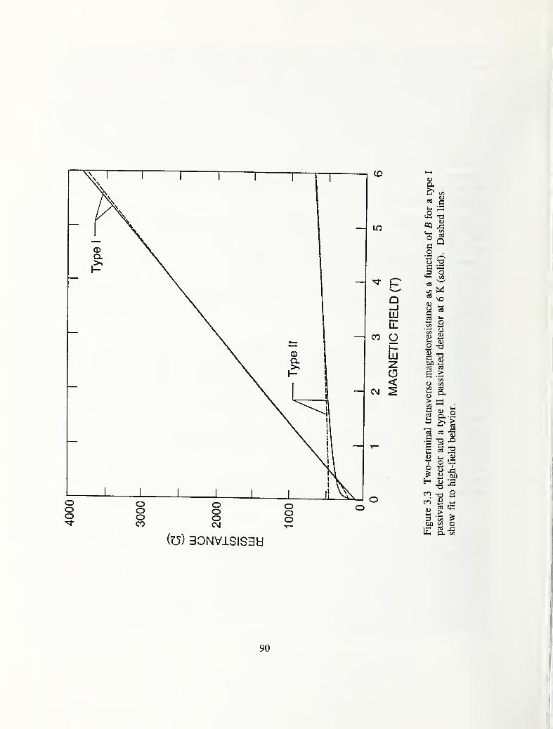
90
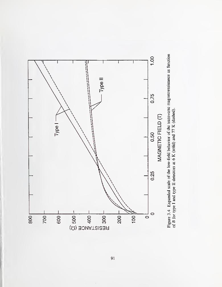
91

92
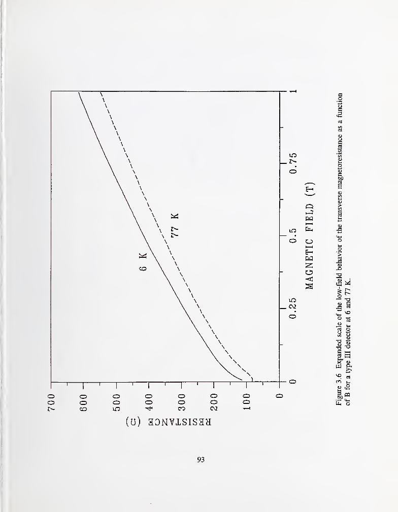
oo
ooCO
ooOO O
OCO
OOC\2
OO
aooa
0)
CO
<U
«1
I
Is
O^ ti
T3 ^
-4—*
CO M
Wh O
(o) aoKivisisaH
93

3 (U
tin r^
(u^) aoNvisisan
94
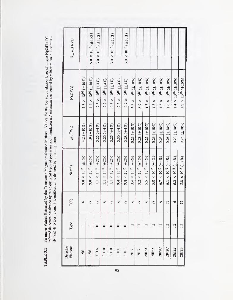
^ 3^ i•a _.
00
3: =
?Lc a.<^ *co o
>^ 3Si* ^— >iCO 73
<U
^ o
§ -a
a
o 2J
S -a
o "t*5 -
. 3"O So ja
2 s sc —
g M c
00 O ^-1) —
=°
S >- o1) 5^55 C «^
^ -s s
y > S•i: « S>< S —
c/3 00<U Ui Ui
_3 O Ooj tj tj
'!> 3 aS "a -a
y "S cE 1-1 u
eu .2 13
I
a.
Z
>e
s
H
Q W
6?o+1
X
q
6§o-H
X
q
6§o+1
Xo
o-H
q
6?o+1
00
5?o
-H
X00
-H
X
-H
00
6?
+1
oo
65
-H
X
6§o+1
X00
00
6?o-H
Xas
6?o+1
X
65o-H
XCO
65o+1
X
65o+1
X
65oJ—t
-H
X
65o-H
65o+1
65
+1
CN
65
-H
CN
65
+\
CN
65
+1
oCD
65
+1
ooCN
65o-H
CN
65o-H
00CN
65o-H
CN
o
65o+1
CN
65o+1
CN
d
65o-H
soCN
65O-H
CN
d
65
X
qas
65
-H
X
qas
65CN
-H
65CN
65CN-H
65CN-H
X
65CN
+1
X00
0\
65
-H
X
65
-H
XCN
65
+1
Xin
65
-H
Xo
65
-H
so
65 65
-H
so
so
CN
SO
CNrn
CQ S U—1
CN CN
<CNe
<CN
3CN
uCN
BCN
uCN
CQCN
3CN
65o+1
X
65o+1
soCN
65
-H
oo
CN
95
A comparison of elements A, B, and C of detector 2III2, shown in figure 3.7, with the measured
responsivities, shows how the accumulation-layer properties correlate with performance. At 77 K the
inverse ratios of the densities and /xA^ products of the elements B and C to element A are 0.86 + 0.03
and 0.82 + 0.03, respectively, while the corresponding ratios of the responsivities are 0.91 ± 0.01
and 0.82 + 0.01, respectively. The uncertainties given here are from the residuals resulting from the
DATAPLOT fits. The agreement is good, which shows the controlling effect of the top accumulation
layer.
In order to obtain information about the bulk, bottom accumulation layer, and contact resistance, the
top layer conductance determined from the fit can be subtracted from the total conductance at B = 0.
Variations in this conductance difference as well as in the top-layer conductance from detector to
detector can be used to determine when the process is not in control. The reasons for the variations
can then be diagnosed. For example, the conductances of elements A, B, and C of detector 2III2 at B= 0 and at 77 K are 8.33 x 10"^, 9.01 x 10"^, and 9.80 x 10"^ S, respectively. Subtracting the
respective top-layer conductances leads to the remaining conductances of elements A, B, and C which
are 6.77 x 10'^, 7.21 x 10"^, and 7.88 x 10"^ S, respectively. If the bulk conductance is the same
for all three elements, these variations would be due to the bottom accumulation layer.
D. Conclusions"
In conclusion, a practical magnetoresistance method has been demonstrated for measuring the carrier
density and Hall mobility of a semiconductor layer by using only a two-terminal configuration, a
situation applicable to a number of industrially relevant devices. An equation has been fit to
published calculations of this phenomenon so that it can be applied to a wide range of rectangular
geometries. Application of this technique to four GOES HgCdTe PC infrared detectors gives results
which are in excellent agreement with previous Hall data, showing the validity and usefulness of this
method. The variation in the electron density of the top accumulation layer of three elements of a
multi-element detector was shown to correlate with the responsivity. The reduced leakage and
increased electron density of the type II and type III processes are shown to be the reasons for their
improved performance characteristics. This technique can be used in the future by the detector
manufacturers to characterize their processes and thereby improve detector performance.
96

PART 11 - OTHER CHARACTERIZATION STUDIES
4. BONDING, METALLIZATION, AND PACKAGING FOR GOES AND TIROS INFRAREDDETECTORS
A. Overview and Rationale^
Evaluation studies of GOES HgCdTe detector packaging were made at NIST during FY 1991 and
1992. Problems that can reduce the yield (increasing the cost) and/or reliability of the devices were
found. Several such problems were docimiented in earlier reports (see NISTIR 4687, September
1991) and in NCAA program reviews. Others are retained in files of NIST's scanning electron
microscope (SEM) studies of these devices. Therefore, work was done in FY 1992 in the area of
detector packaging to improve the above situation and, hopefully, to prevent surprise problems from
arising that can delay launch dates and necessitate retrofits or otherwise increase NOAA satellite
costs. The objectives and rationale of the NIST packaging work during FY 1992 are given below.
1) Develop a set of Recommended Practices (guidelines) for packaging of NOAA space sensors
(detectors). This will include recommendations for reliable wire bonding (interconnections),
package electroplating, device metallization, and molecular cleaning methods.
Circulate the Recommended Practice to appropriate detector contractors and other interested
organizations for their comments. Their comments will be evaluated, negotiated, and
incorporated in the final document. This document will be given out to appropriate contractors
for implementation on future NOAA infrared sensors.
2) Request the detector manufacturers to submit examples of detectors (electrical or optical rejects)
mounted in packages designed for incorporation in NOAA satellites. NIST will then examine
(with SEM and/or other appropriate analytical methods) for compliance with the above guidelines
in (1), with emphasis on potential reliability and yield enhancement. If problems are found,
NIST will then:
a) Assist sensor (detector) contractors with necessary information, visits, and training, so they
can package devices in conformance with these guidelines.
b) Serve as packaging and materials science consultants for any problems that may arise in
NOAA infrared detector manufacturing, and present training seminars on reliable packaging.
3) Many wire bond yield and reliability problems are traceable to the lack of molecularly cleaned
bonding surfaces. Studies will be carried out to establish the best cleaning methods that are
compatible with the normal HgCdTe detector packaging methods.
Large integrated circuit (IC) packaging houses make hundreds of thousands of devices and
millions of wire bonds per week. They can therefore employ a number of engineers who are
experts on bonding. However, infrared sensor companies make so few bonds that no one
engineer can specialize in this area; thus such companies may have more bond yield and/or
reliability problems than the IC companies.
97
4) Cooperate with other NIST HgCdTe detector studies, such as preparing samples for low
temperature Shubnikov-de-Haas and other measurements.
6. Accomplishments
A first version of the"RECOMMENDED PRACTICE FOR THE WIRE BONDING AND
METALLIZATION USED IN RADIATION DETECTORS PREPARED FOR USE IN GOES.TIROS. AND OTHER SPACECRAFT " was written and circulated to eight organizations and, in
some cases, to several individuals within an organization. After receiving responses (several did not
respond) when questions remained, those individuals were contacted for resolution. The final
document includes references to ASTM as well as to various Military Class "S" (space) specifications
and standards. The "Recommended Practice" document is in Section C. Because of some late
responses there was not time to recirculate the new document for final comments. Readers are urged
to make any such comments as soon as possible after receiving this report. If significant changes are
suggested and made, then the "Recommended Practice" will be revised and republished later as
final. The document was also presented to a standards organization, ASTM Subcommittee F-1.07
(the wire bonding committee) at its meeting on January 28, 1993 for additional comments from a
different but very knowledgeable audience.
A total of six visits were made to three GOES and TIROS infrared detector manufacturers during FY1992. The first visit to each site was made to evaluate their production lines and processes. Later
visits were made to help them with the packaging of their detectors including, in one case, a 2.5-hour
seminar on wire bonding and the reliability of the metallurgical systems used in packaging HgCdTedetectors. Over 30 people attended that seminar. A more informal, hour-long presentation was madeat another company where six/seven engineers and management personnel attended. Extra time was
spent in their packaging laboratories discussing equipment, etc. A study was made of detectors from
one manufacturer and several defects were found (the results were presented at a GOES project
review at NASA Goddard on July 10, 1992). This information, with proposed solutions, was also fed
back to the manufacturer to help them improve their product.
Many wire-bond yield and reliability problems are traceable to molecular-level contamination of the
bonding surfaces resulting from handling, epoxy outgasing residues, etc. The high-reliability
microelectronics hybrid industry routinely uses oxygen and argon plasma or ultraviolet-ozone (UV-
ozone) cleaning procedures to greatly enhance their wire-bond yield and reliability. The HgCdTedetector industry has been afraid to use such cleaning methods before bonding because of possible
damage to the detectors or to their surface coatings. These concerns have never been documented,
but there is some possibility that oxygen plasma cleaning could attack the antireflection coatings.
Therefore, NIST proposed to study the effects of UV-ozone cleaning on HgCdTe detectors. This
work was planned to determine whether the cleaning had any effect on the sensitivity and noise of the
detectors, as well as any effect on the various optical absorptive coatings that may be used inside the
housing (but not on the device).
Preliminary UV-ozone cleaning experiments were carried out at NIST on available detectors and
absorptive coatings. No physical damage was observed. However, there was no equipment available
at NIST to evaluate any possible optical or electrical damage to the detectors. Thus, for these
additional measurements, it was necessary to visit two cooperating detector manufacturers and
perform the experiments there. For this, the UV-ozone cleaning equipment was hand-carried [on
airplanes] to the manufacturers' locations. Previously tested detectors were irradiated in the NIST
98
equipment at their plants, but retesting for electrical and optical properties had to be scheduled for a
later time. One organization has reported its first set of measurements made within one week of
irradiation. The data indicate that the detector noise measurements show no change due to UV-ozonetreatment. However, the infrared sensitivity was found to decrease in all samples by an average of
11%. The organization plans to remeasure the detectors in 3 months to see if this decrease is
temporary or permanent. If temporary it should be removed by minimal heat treatment (perhaps an
hour at 80 °C). However, if the sensitivity loss is permanent, then another method of cleaning will
have to be investigated. Cured black light-absorbing paint was irradiated at NIST, and no damage to
its light-absorbing properties was detected.
In addition to the possible detector damage studies, other experiments were performed to show the
effects of cleaning on wire bondability at the manufacturers' plants. Problems immediately arose at
one manufacturer because the intended bonder was in use and another had to be substituted. This
bonder was not in good condition and did not make reproducible bonds (the work-holder was not flat,
the bonding tool moved laterally during bonding, etc.) Also, some of experiments that were
performed appeared to show that cleaning actually decreased bondability (something that has not been
observed before and is presumed to result from the bonder problems). The organization planned to
obtain their own UV-ozone cleaner and rerun the experiments later. Other problems relating to
peeling metallization were found at another manufacturer. Thus, in order to reach any conclusion,
both of these experiments must be continued.
Ten special HgCdTe infrared detectors received from manufacturers were prepared and mounted in
low-temperature carriers for Shubnikov-de-Haas and other liquid-helium temperature measurements.
New removable adhesives that would tolerate these low temperatures had to be found, and special
carriers (packages) were made. Several repairs to soldered or wirebonded interconnections were
affected. In addition, various other techniques such as microsoldering had to be developed.
C. Recommended Practice for Wire Bonding and Metallization Used in Radiation Detectors
Prepared for Use in GOES, TIROS, and Other Satellites
1) The bonding wire should be made of the same metal as the bond pads on both the detector and
the package. This is normally gold. If there is a difference between the metallization on the
chipside and the packageside, then the wire material will match that of the chip-side bond pads,
a) Electroplated (or vapor deposited, etc.) gold [metal] should be pure, soft and uniform in
optical appearance and thickness. It should contain < 1 ppm of thallium and have <50 ppmtotal impurity content. The hardness should be < 80 Knoop. Any unusual surface
appearance should be investigated with appropriate magnification (lOOx optical microscopy
or up to 400x for a scanning electron microscope). If blistered, cracked, or peeling, it
should be further investigated (see Mil-Std-883, Method 2010.10, 1 3.1.1.4). It is clearly
rejectable if a metal-deposition-defect is in the bond pad area and is equal to or greater than
one quarter the area of the bond nugget and positioned so that the bond must be placed on
top of it. The same condition should be applied to an external soldering area (substituting
solder in place of bond nugget). It is also of concern if the metal defect is elsewhere, since
this indicates that the metallization process is out of control and may therefore produce
defects in critical areas on other packages in the same lot that may not undergo inspection.
2) Bond pads should not be placed on brittle, crater-prone material such as HgCdTe. Special
designs involving (>0.5^m) under-layers of hard metals such as titanium and/or tungsten on
99

brittle materials may be acceptable if demonstrated to prevent bond cratering. (Such layers have
long been used to prevent cratering in silicon and gallium arsenide devices. For HgCdTedevices, a hard underlayer thickness of 0.5 to 1 ixm is a good starting point, followed by > Ijixm
of gold.)
3) The bond pad metal must be clean and uniform to be wire bondable with a high yield.
a) Cleaning of the open, packaged, detector should be done (with plasma (O2 or Ar) or
UV/Ozone) within 2 hours of bonding, if such cleaning processes do not damage the device.
Vapor degreasing has been used, but it is not as effective as one of the molecular cleaning
methods above. (The recommended method of cleaning HgCdTe detectors before bonding is
currently being investigated by NIST in cooperation with two detector manufacturers.)
b) Any evidence of scratching the detector or package bond pad metallization, either during
handling or to mechanically clean the surface intentionally in order to enhance bondability,
should be questioned and will be cause for rejection if more than 25% of the bond pad area
is disturbed (see Mil-Std-883, Method 2010. 10, t 3. 1 . 1 . 1 .h). Probe marks and carefuUy
removed test bonds, are exempt unless their remains are so large as to interfere with final
bonding.
c) Any evidence of rebonding, either lifts or residual pieces of earlier bond attempts (other than
necessary test bonds), should also be questioned. Any of these evidences may be cause for
rejection or performing a nondestructive wirebond pull test to verify the bond integrity if
they interfere with the final chip-to-package bonding. (Note: Use of the nondestructive pull
test will raise the loop height, and may result in the wire interfering with a closely placed
lens or some other package height constraint.)
4) Bonding requirements and methods for gold-gold interfaces
a) Although gold-gold bonds can be made reliably at room temperature, the bonding window is
narrow and any surface impurities will reduce the bond yield significantly. The highest bond
yield and the broadest bond parameter window occurs when the interface is heated.
Therefore, when using ultrasonics, it is also desirable to apply work-stage heat or use a
heated bonding tool. The latter must be 200 - 300 °C to be helpful. In general, use the
highest bond interface temperature possible (up to 300 °C) considering the thermal
limitations of the device, epoxies, and other packaging materials. Even a 75 °C heated
substrate improves the bondability and reliability of a gold-gold bond.
b) The wedge bonding of gold wire to gold pads normally requires the use of a special gold
bonding tool, which will have a cross-groove and/or a roughened surface.
c) Wire bonding takes place at a higher bond yield if the surfaces are flat (perpendicular to the
axis of the bonding tool). Round or angled surfaces reduce the bond yield and should be
avoided. If they cannot be flattened, then special care should be taken, such as tipping the
substrate, bonding straight along the highest portion of a cylindrical surface, etc., in order to
maximize the bond yield.
100

5) The bond appearance should be normal.
a) Ultrasonic wedge bonds should not be over- or under-deformed (the range for reliable gold
wedge bonds is between approx. 1.5 to 2.5 wire diameters and 1.5 to 2.0 wire diameters for
aluminum wire bonds). There should be no evidence of smearing, either on the bond itself
or on the adjacent bond pad area. (When gold wire is wedge bonded to gold at low
temperature (< 100 °C), the bonding window is narrow and bonds with low deformation
(< 1.5 wire diameters) may not be reliable.)
b) The bond heels should not be cracked, and particularly, if a cross-grooved bonding tool was
used for gold bonding, both the front and rear of the bond should be normal. (For example,
the front portion, in front of the groove, should be neither separated from the body, over-
nor imder-deformed, nor be missing.)
6) Wedge bonds should be tested using an appropriate statistical sampling method (e.g., MIL-M-385 lOJ, Appendix B) using the pull test for machine setup and evaluation. Electrical reject
samples may be used for setup purposes, and several bonds may be placed on one pad if there is
room. Under some conditions, the nondestructive pull test may be used on completed devices,
where critical verification is necessary. Use class "S" requirements in the test methods below (if
applicable).
a) Use Mil-Std-883, Method 2011 for the destructive pull test.
b) Use Mil-Std-883, Method 2023 for the nondestructive pull test.
c) Use ASTM F 1269-89 (Ball Shear Test) if ball bonds are used.
7) Fine gold wires (<75 ^m diameter) must not be soldered, but must be welded by a standard
method used in microelectronics (thermosonic, ultrasonic, split-electrode electrical discharge,
etc.).
8) This Recommended Practice may also be applied to bonding in non-HgCdTe types of detectors
such as bolometers, etc.; in that case the same metal (gold in 1) may be omitted, and either the
pad and/or the wire may be aluminum. (If the wire is aluminum, then no bonding advantage is
obtained from using special bonding tools.)
a) On occasion, conductive polymers (e.g., gold- or silver-filled epoxy) are used instead of
metallurgical welding to obtain electrical conductivity. This presents many complex material
choices and cannot be addressed by this Recommended Practice. (For example, silver-filled
epoxy should not be used to electrically connect wires to aluminum surfaces, but under some
circumstances may be acceptable for use at cryogenic temperatures.)
D. Glossary
HgCdTe is mercury cadmium telluride, a semiconductor material used for far-infrared detectors.
This material is very brittle and has a low fracture toughness. It craters easily. It is typically used at
cryogenic temperatures < 100 K.
101

Cratering, crater-prone. Cratering refers to crystallographic damage in a semiconductor underneath
a bond. It can range from microscopic damage to large divots of the semiconductor that are pulled
up during bonding or in a pull test. Brittle materials with low fracture toughness crater easily during
bonding, and HgCdTe is such a material.
Military Standards: Mil-Std-883. This is the "Test Methods and Procedures for Microelectronics."
The specific version referred to in this Recommended Practice is 883D, 15 November 1991.
Although it was not specifically designed for spacecraft detectors, its class "S" provisions as well as
its bond pull test requirements are used almost universally for other parts of spacecraft electronics.
Only those parts applicable to this Recommended Practice are cited. MIL-M-38510. This is
"Military Specification, Microcircuits, General Specification For" This is cited for its statistical
sampling methods.
Yield is used in this document to mean the fraction of acceptable wire bonds produced in the
manufacturing process.
E. Typical Bonding Characteristics and Appearance of Plated Gold Films
(Not a part of the Recommended Practice~for information only)
(1) Gold films that bond well and are reliable:
a) Are pure yellow in color.
b) Are uniform, matte, and lusterless in appearance.
c) Are smooth and free from pits, blisters, or other blemishes.
d) Are soft (<80 Knoop), ductile, and dense.
e) Have <50 ppm of total impurity content.
f) Have < 1 ppm thallium and low hydrogen content for Al wire bonding.
g) Have a wide bonding parameter window.
(2) Gold films bond poorly and/or are not reliable if they:
a) Appear dark, have large nodules, or are very bright.
b) Shed minute particles on handling.
c) Have a lenticular or columnar structure and/or high porosity.
d) Have a high hydrogen or thallium content and/or >50 ppm total impurities.
e) Are hard, nonductile, and/or have high internal stress.
f) Give poor corrosion protection.
g) Have a narrow bonding parameter window.
(3) A pragmatic test to evaluate gold films for aluminum ultrasonic bonding: make aluminum bonds
to the film, bake 300 °C for 1 h, and reject if bond lifts in pull test. (This is based on Mil-Std-883,
Method 5008, f 3.5.3.3). This is a destructive test and is often used to screen packages or films
before acceptance from a vendor. It would not be used on a completed detector.
102
5. SEMICONDUCTOR ELECTRONIC TEST STRUCTURES: APPLICATIONS TOINFRARED DETECTOR MATERIALS AND PROCESSES
A. Introduction
Test structures are microelectronic devices which are fabricated by the same processes used to
manufacture semiconductor electronic products, and that are used to measure selected material,
process, or tool parameters by means of electrical tests. Properly designed test structures can be used
to evaluate semiconductor materials, to determine and monitor process-centering parameters, to
measure critical device and circuit parameters (which can be input to device models), to identify and
quantify yield limiting defects, and to measure processing tool performance.
Test structures are essential tools for fabrication process development and process maintenance of
silicon integrated circuits (ICs) and gallium arsenide monolithic microwave integrated circuits
(MMICs). However, test structures have not been as widely applied in the process development and
manufacture of infrared detectors, nor have the ways in which they are used been well documented in
the open literature. Considering the substantial impact of test structures on other semiconductor
products, the current state-of-the-art applications of test structures to HgCdTe-based IR detectors have
been reviewed. The smdy had several goals:
1) To communicate and encourage application of the substantial experience gained with test
structures in Si and GaAs to HgCdTe IR detectors;
2) To document test structures, appropriate to IR detector technology, so that they could be more
readily assembled into test chips;
3) To determine new ways in which test structures could be applied to improve HgCdTe uniformity,
to increase detector yield, and to enhance performance of detectors;
4) To identify test structures and measurements to complement and correlate with the Shubnikov-de
Haas and other magnetotransport measurements.
To meet the goal of communicating to the IR detector community, the results of this study were
presented at the Measurement Techniques for Characterization of MCT Materials, Processes, and
Detectors Workshop in Boston, Massachusetts, on October 16, 1992. A publication entitled: "Review
of Semiconductor Electronic Test Structures with Applications to Infrared Detector Materials and
Processes" has appeared in the workshop proceedings published in Semiconductor Science and
Technology in 1993 [5.1]. This publication is the most complete review of test structures applied to
IR detectors and contains suggestions on how to improve IR detector process control, yield,
performance, and reliability through the intelligent application of test structures. The complete paper
is reproduced in Appendix B.
A major element of this study was a comprehensive review of specific test structures used by the IR
detector industry. A thorough review of the literature concerning applications of test structures to IR
detectors was conducted. Details of device design and measurement methodologies were also
considered. In addition, experts in the electrical characterization of IR detector materials and devices
were consulted. A site visit to Loral Infrared and Imaging Systems was conducted; other
consultations took place via telephone. A variety of reasons were suggested for the underutilization
103
of test structures with IR detectors:
1) The relatively small numbers of devices required and the nature of the market have not demanded
large yields to satisfy product demand or to assure profitability. However, even if production
goals can still be satisfied with a low-yield process, the long-term reliability of devices fabricated
with a low-yield process could be compromised.
2) The need to test devices at low temperatures and as a function of irradiation has often been most
easily satisfied by packaging devices before any testing. Consequently, development and use of
low-temperature automated probe stations to acquire statistically significant amounts of data at the
wafer level and before packaging (a major application of Si and GaAs test structures) were not
vigorously pursued.
3) The perceived need to package devices before test resulted in a conclusion that completed
detectors were their own best test structure. A larger emphasis was placed on the quality of
detector performance rather than the direct measurement of specific material and process
parameters with test structures. Instead of test structure measurements, the electrical
characteristics and figures-of-merit of detector elements have been used to deduce some material
parameters, and as a general indicator of device and process quality.
4) Early on, the poor quality of HgCdTe and resultant low yield of fabricated devices has,
paradoxically, encouraged a reluctance to devote valuable HgCdTe surface area to test structures.
Without test structures to verify process and material parameters, poor detector performance or
unexplained failure of elements in an array is often attributed, without evidence, to low-quality
starting material.
The experience of both the silicon IC and GaAs MMIC industries has shown that a comprehensive
test structure program is essential for effective process development and maintenance.
Communication of this previous experience would encourage wider applications of test structures in
the manufacture of IR detectors. Thus, a second critical aspect of this study was to review the
general principles of applying test structures determined through experience with silicon ICs and
GaAs MMICs. Much of this experience is in contrast to the practices described above. For example,
it is accepted that for silicon ICs, an intelligently selected and applied set of test structures is more
informative than finished product performance in the diagnosis of which specific process steps may be
limiting detector performance or yield. Test vehicle (chip) design methodology facilitates judgment as
to the appropriate number and kind of test structures, as well as a percentage of substrate area to
devote to test structures, even for processes with very low yields.
The third aspect of this study was to extract principles and ideas for test structure applications from
the Si and GaAs experience that could be used to further enhance the manufacturability of IR
detectors. The central lesson is that yield improvement requires improved process control by means
of the intelligent application of test structures . An increased emphasis on applications of test
structures is indicated for IR detectors. While the methodologies developed from previous experience
can serve as a model for implementing test structures as tools for IR detector process development
and control, substantial effort will be required to:
• Determine what information is needed from test structures by correlating detector performance
and yield with material and process parameters.
104
• Determine how that information will be obtained by correlating the output from test structure
measurements with relevant HgCdTe material and process parameters.
• Develop and document standard, well-characterized test structure designs as cells in a CADlibrary.
• " Develop and document a detailed test plan.
• Develop and document detailed data analysis procedures.
Data acquisition may be simplified and accelerated by development of automated probe stations which
are compatible with low-temperature measurements and which use lightly contacting or noncontact
(i.e., low-damage) probes.
B. Conclusions
The conclusions of this study can be summarized as follows: Greater application of test structures to
IR detector manufacture could lead to real improvements in the yield, reliability, and performance of
the detectors. The previous experience with test structures in the Si and GaAs industries provides a
useful guide and methodology for expanding the applications of test structures to IR detectors.
However, further applied research will be necessary to optimize these applications of test structures.
The experience of researchers at the National Institute of Standards and Technology is a resource for
extending the current applications of test structures to IR detectors. Potential areas of impact will be
to augment the design and applications of the existing test structures, to develop new test structures
aimed at specific process or material problems, and to develop comprehensive test structure
implementation plans. Cooperation among the users can further increase the impact of test structures
on IR detector manufacturability. NIST and industry should work together to develop common test
structures and implementation approaches.
105
6. SCANNING CAPACITANCE MICROSCOPY: A NONDESTRUCTIVECHARACTERIZATION TOOL
A. Background
Scanning Capacitance Microscopy (SCM) is being established at NIST as an internally funded
initiative. SCM is a type of scanning probe microscope (SPM), like the scanning tunneling or atomic
force microscopes (STM or AFM). SPMs produce images by recording the strength of some
interaction between a mechanical probe tip in close proximity to a surface as that probe tip is scanned
in two-dimensions above the surface. Nanometer resolution is readily achievable.
Scanning Capacitance Microscopy is expected to be sensitive to nanoscale variations in dopant
density, composition, defects, mobility, and charge within a semiconductor. Because of these
capabilities, SCM will have some very important applications to IR detector material, process, and
device characterization. For example, the spatial resolution of the SCM will be such that
performance difference between two photoconductive detector elements, which appear to be identical
by visual inspection, can be investigated by imaging the electrical properties of the active region
between the contacts. SCM has the potential to provide nondestructive prefabrication material
screening, so that detector fabrication is undertaken by using only the highest quality material.
Examination of cross sections of epitaxial layers or diffused regions will allow the dopant and
compositional variations to be determined with unprecedented resolution and accuracy. In addition,
topography, such as epitaxial island thickness and uniformity, can be measured with an AFM.
One possible implementation of SCM uses the Metal tip of an STM and the Insulating air gap
between the tip and a Semiconductor to form an M-I-S capacitor. Capacitors of this sort have long
been a basic test structure to determine the properties of semiconductors. The SCM provides an MIScapacitor that is nondestructive, highly localized, and mobile. Thus, many of the measurements made
with capacitive test structures on semiconductors could now be implemented as a microscopy; i.e., the
spatial variations of the measured parameter could be mapped into an image. The concept of a
scanning capacitance microscope was demonstrated by Matey in 1985 [6.1], and a capacitance probe
was first integrated with an STM by Williams in 1989 [6.2]. SCM has also been demonstrated by
using an AFM by Barrett in 1991 [6.3].
B. Applications of SCM to GOES and Related Infrared Detectors
Scanning Probe Microscopes are expected to have an enormous impact on the semiconductor
electronics industry, perhaps surpassing that of electron microscopy. Significant applications are
envisioned not only in the silicon integrated circuit industry, but throughout the wide range of
industries based on semiconductors, including infrared detectors based on HgCdTe and other
materials. SPMs will be important because of these unique capabilities:
1) High Resolution — Atomic resolution is "easily" achievable with STM and other SPMs. As
device dimensions are reduced below a micrometer, SPMs allow features to be seen that are
beyond the resolution of optical or electron microscopes.
2) Nondestructive — In general, SPMs are noncontact and nonintrusive. Microscope vendors
have begun building stages compatible with in-line examination of 200-mm-diameter wafers.
Thus, most nominally flat surfaces are accessible, as well as some types of packaged devices.
106
3) Sensitivity to material properties — SPMs exist that are sensitive to various physical
parameters of importance to semiconductor electronics. These include the AFM which is
sensitive to surface topography, SCM which is sensitive to the parameters that determine
capacitance (such as dopant density), as well as other microscopes such as a Kelvin probe
microscope which is sensitive to work function differences.
The possible applications of SCM to metrology problems of importance to GOES and related infrared
detectors include:
Materials Characterization
Nanoscale microscopy of bulk electrical properties
Dopant density
Composition
Defects
Interface properties
Mobility
Pre-fabrication wafer screening
Characterization of nanostructured materials, such as structures grown by molecular beam epitaxy
Process/Device Characterization
Junction profiling
Insulator/passivation charge mapping and manipulation
Topography and surface roughness
Fine-scale C-V measurements (and associated analysis)
Insulating layer integrity/defects/damage/uniformity
Metallization integrity/grain structure
Failure Analysis
Process-induced damage
Electrostatic discharge damage
Process fault and material diagnosis
C. Establishment of Facility
The significant challenges in bringing SCM from the lab to a practical (potentially in-line) analytical
technique are to 1) develop measurement procedures, 2) improve signal-to-noise and sensitivity, and
3) develop the theoretical interpretation and models to relate measured signals to relevant material
parameters.
A Digital Instruments Inc. Nanoscope III^ with a large sample stage was procured as the basis for
the NIST SCM. A schematic of the interface of the SCM with the AFM is shown as figure 6.1. The
system can perform both STM and AFM and has a fully automated stage with 200-mm wafer
Certain commercial equipment, instruments, or materials are identified in this paper in order to
adequately specify the experimental procedure. Such identification does not imply recommendation or
endorsement by NIST, nor does it imply that the materials or equipment used are necessarily the best
available for the purpose.
107
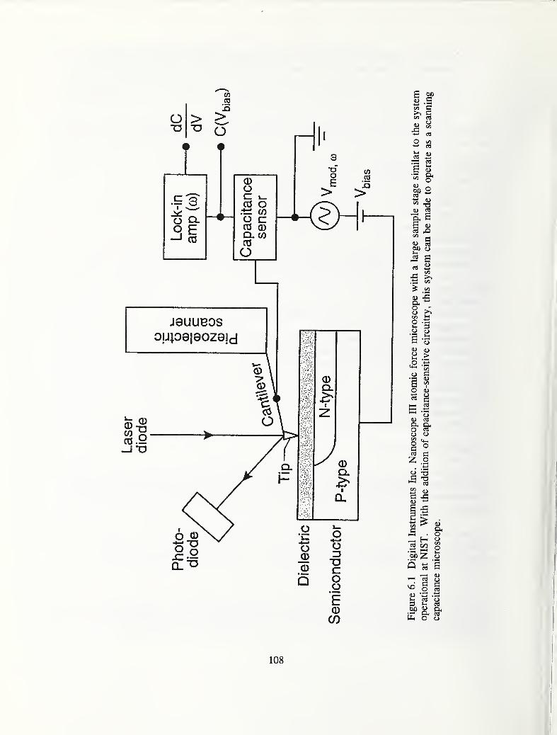
Co
- ir:
108
capability. Scanning capacitance microscopy will be initially implemented in the atomic-force-
microscopy mode. SCM in the scanning-tunneling-microscopy mode will also be investigated in the
coming year. The SCM will be an important addition to existing efforts to characterize and screen
infrared detector materials and devices.
Capacitance-sensitive circuit
After Matey [6.1] and Williams [6.2], the capacitance-sensitive circuit from an RCA video disc player
will initially be used. This provides an inexpensive, high-sensitivity, and miniaturized capacitance
sensor. Other means of capacitance measurement will be investigated with the goals of increased
sensitivity and dynamic range of the capacitance measurement.
Modeling effort
An effort to model the measurement of capacitance with the SCM probe is ongoing. The SCMcapacitor is in a hemispherical geometry rather than the more usual and more highly studied parallel
plates. The initial thrust will be to numerically simulate the electromagnetic field between the probe
tip and semiconductor by using currently available software. While several groups have demonstrated
the concept of SCM, the measured signal has not yet been quantitatively related to the semiconductor
dopant variations.
It is worth noting that applications of the interactions of a scaiming probe tip and a semiconductor,
especially when subjected to transient electrical and optical signals, are still a new area of
investigation. It is likely that many semiconductor parameters will ultimately be accessible with some
type of SPM.
D. Preliminary Results
At the writing of this report, the AFM/STM which will form the basis of the SCM facility has been
operational only a short time. AFM images were made of some photoconductive detector elements to
illustrate the potential resolution and image quality of an SCM based on the AFM system. Images
were made at room temperature and in air on a packaged device. No sample preparation other than
mounting the package to the microscope stage was needed.
Figure 6.2 is a low-magnification AFM image showing parts of three photoconductive detectors.
AFM provides a precise means of determining layer heights and device topography. In the initial
implementation of SCM, AFM will be used to measure material topography simultaneously with SCMmeasurements. An independent measurement of topography greatly simplifies the interpretation of the
scanning capacitance image.
Since an SPM acquires images as arrays of digital data, rapid image manipulation and analysis is
possible. Figure 6.3 shows a cross-sectional analysis of an AFM image of the boundary between the
passivated active layer and the metal pad of a detector element from figure 6.2. The AFM image
reveals a 150-nm dip in the passivation layer at the probe-pad boundary and a step in the probe-pad
wall which could not have been as easily imaged with an optical microscope or SEM. Statistical
analysis of topography or surface roughness is also readily available.
109
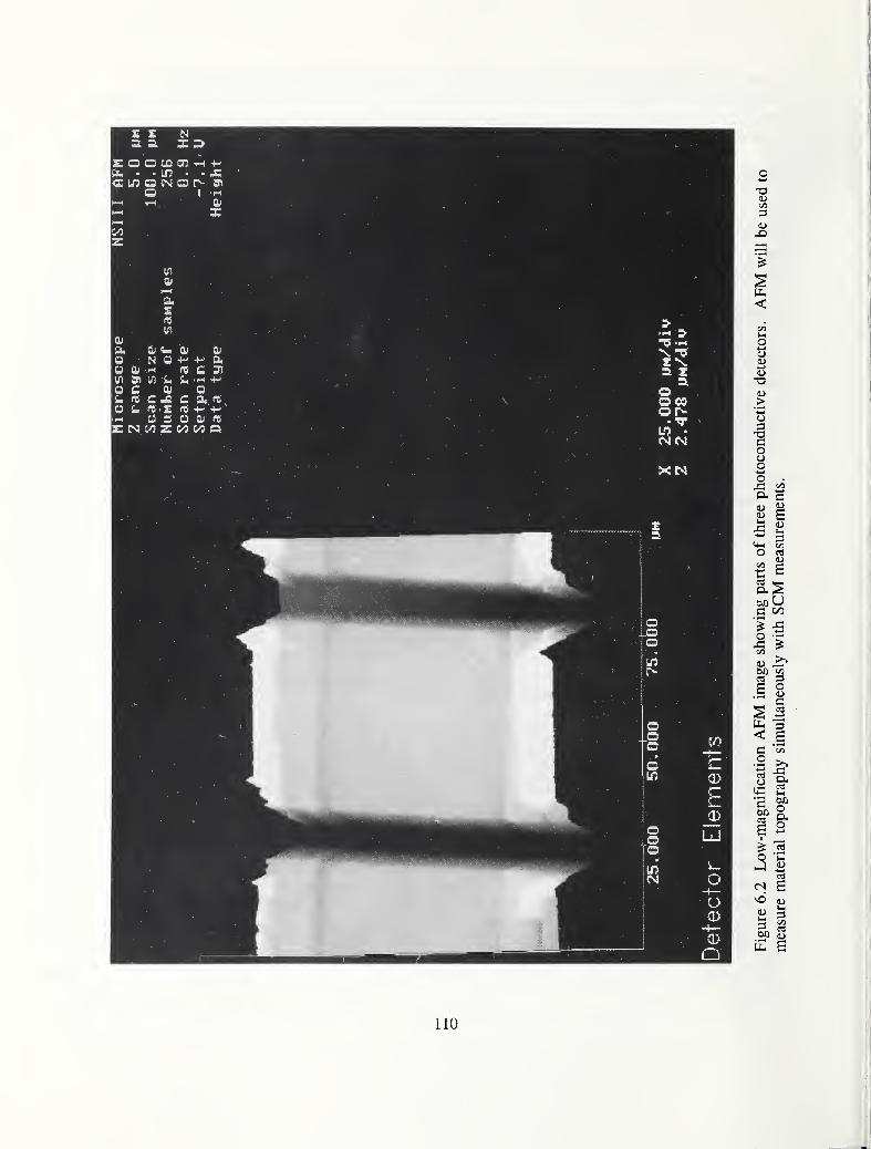
!
110
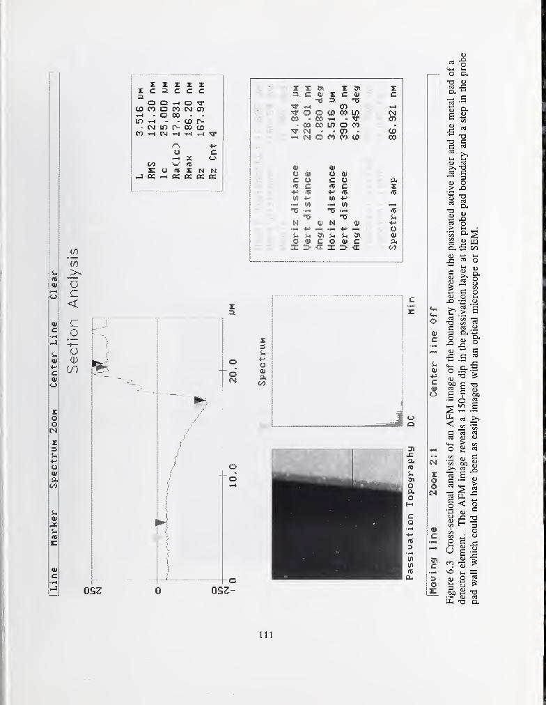
^-8
z z z z zX c c c c=1.
o o o TCO o tr> CM CD
1—1 o 00m i~i 03 r-(M in r- 00
CO >—
1
CM 1-1 r-l
r\u c—
<
XC/3 w (6
z: o IV Z N Nr—
4
cc cc cc
01
01
c
u014-'
c01
zoo
o01
a.
01
«6
01c
DC<co
00
z z z 9^ zc at z c c
"T5 a.CDo O 00 C>1
CO CO • (J)- 00 00 o 00 •
" CD(^1 o CO 00 CO CO
4t
o <U O «c O c o fit
c c z
w ww w
-T5-0
N at N *i>
*^ O"Ji 01
O a» c O c iXX •a: X 3 CE (/>
c
oa>
c
U<D
co
ca
ftXu.ro
z3) oO oo. tsiof-H
co
• l-l 0)-f- c(13
3
in ?n1/1 cIt
flu
osz-
111

"1 0)
112

Figure 6.4 shows a higher magnification AFM image of the edge of the active area of a detector
element. Considerable structure to the topography is seen clustered along the edge of the active area
with resolution of less than 1 ^m. Resolution of AFM is less than 10 nm and would permit the
surface roughness of materials and device layers to be quantified. SCM will certainly be capable of
similar resolution which would be sufficient for planar materials characterization. Resolution of
100 nm has been demonstrated with SCMs similar to the one being constructed at NIST, enabling the
dopant variations across p-n junctions or heterostructures to be quantified.
It is difficult to identify the origin of the fine structure seen in the topography at the detector edge
without more extensive measurements. It may be due to particulate contamination concentrated by a
wet process step before or after passivation deposition. Indeed, development of SCM will permit the
electrical effects of such topography disturbances to be probed and their likely effects on detector
performance to be evaluated.
E. Summary
Scanning capacitance microscopy is a new, nondestructive metrology tool expected to have significant
applications to infrared detector materials, processes, and devices. SCM will produce images that can
be related to material electrical properties with spatial resolution comparable to the dimensions of
detector elements. SCM applications expected to have a large impact on the quality, yield, and
manufacturabilty of detectors include: nondestructive diagnosis of material variations within the
active regions of detectors, nondestructive prefabrication materials evaluation, and dopant depth
profiling of nanostructured materials.
113
7. NIST REVIEW OF THE GOES CALIBRATION PROGRAM
Contributed by
B. Saunders, C. Johnson, and C. Chromer
Radiometric Physics Division, NIST
A. Purpose
The goals of this task were to investigate the radiometric calibration procedures of the GOES program
and to report NIST evaluation of the calibration capabilities of the prime vendors. Out of this
evaluation NIST was to suggest recommendations for an improved calibration program for the
infrared sensor system on the GOES platform. NIST staff would visit the three main contractors
associated with developing the instruments for the infrared radiometric measurements. Although
LORAL is the main contractor for the GOES program, they were not directly involved in the
radiometric calibrations, and as a consequence, NIST staff did not visit or discuss radiometric
calibrations with LORAL staff.
NIST staff first visited and examined the radiometric calibration programs of the detector vendors and
followed with a trip to the system integration contractor (ITT Fort Wayne) where the final radiometric
calibrations of the GOES satellite are performed.
B. Summary of Visits to Facilities
1) Supplier 2
Supplier 2 supplied the indium antimonide detectors and the associated collecting lens system used for
the short wave infrared channels of the GOES sensor system. The only radiometric calibration
specification that the detector was contractually required to meet was a specified blackbody D* for
bare detectors. These test were performed using a 500-K blackbody as a standard for the blackbody
D* determination. This is a straightforward measurement and is routinely made at a precision of few
percent. NIST observation at Supplier 2 confirmed the measurements were being done according to
accepted practice. Because of the detector sensitivity requirements of the GOES sensors, only one
detector in a hundred met the requirements and could be selected for further processing. At this
point, the calibration program at the detector manufacturer ceases, and the detectors are not further
characterized until they arrive at ITT for integration. The next step at the detector manufacturer is
the fitting of the detector optics onto the detector. The only requirement for the detector
manufacturer is that the optics meets certain fabrication specifications and that the optical elements be
tested for transmittance. The detector manufacturer is not informed about the criteria for the final
selection process for the integrated detector package. The detector manufacturer is not responsible for
the technical operation of the assembled detector after the lens is integrated on the detector. Nocheck or test of responsivity or noise of the lens-detector systems is performed by the primary
manufacturer.
2) Supplier 3
Supplier 3 is the manufacturer of HgCdTe detectors for the long wave channels. During the visit,
NIST staff was shown the manufacturing process for the detector but was not able to review any
calibration program of the detector package. This apparently was due to the fact that the calibration
114
program for the detectors was not operational at the time of the visit. Suppher 3 performs somegeneral radiometric characterizations but does not provide detailed radiometric characterizations.
Limited performance checking is the basis for selection of detectors to be used for the GOES satellite.
C. Recommendations
a. The calibration process must be studied from the fundamental optical physics viewpoint, the
sources of error identified, and their effects on the final measurement determined. Acomprehensive approach to this problem involves writing a measurement equation that
incorporates all the relevant parameters and their relationships.
b. Determine the critical parameters that are needed to characterize and develop a calibration
plan before manufacturing the components. This calibration plan can be done in several
steps. In GOES, there should be a calibration and characterization program for each step of
the manufacturing process. The different components, such as the detectors should be
characterized before proceeding to the next step of reassembly. These detector packages are
the heart of the GOES sensor system and are required to meet specifications that are at the
theoretical limits of the detectors. Presently, the bare detectors are only being tested for
blackbody D*. Although this is a critical parameter, the detectors should be tested for
parameters other than blackbody D*. Parameters that affect detector performance are
internal shunt resistance, spatial radiometric uniformity, stability, spectral responsivity,
spectral D*, and linearity; if any of these parameters is unacceptable, then it is pointless to
proceed to the integration of the lens onto the detector. The parameters such as spatial
radiometric uniformity and geometric radiometric response function (response as a function
of angle) should be determined after the lens is mounted on the detector.
c. Detailed records showing the history of the contributing test and changes should be
maintained. These records should follow the component though its incorporation into the
satellite. These records could be used to determine the stability and performance of the
detectors [aspect of the sensor system.]
d. There should be a coordinated effort to maintain calibration assurance between the different
manufacturers and the assemblers. This will help each manufacture plan a suitable and
appropriate calibration program. In NIST's investigation, it was found that the different
manufacturers of the detectors involved did not know how the detectors were going to be
tested in the next stage. Not only is this costly but a lot of valuable expertise is not passed
down the manufacturing chain. Also, the manufacturer is not held responsible for the
performance and ability of his product to integrate it to successive stages of the assembly.
Each manufacturer should be held responsible for meeting the specification of the next stage.
e. To achieve a reliable sphere source, considerably more attention to the calibration and care
of the sphere will be necessary. The sphere should be calibrated more frequently and a
history of the calibration maintained. Departures or significant change from the baseline
need immediate attention. The calibration schedule of the sphere should closely bracket the
calibration of the GOES sensors.
f. Since the final product is a radiometric calibration problem, staff trained in radiometric
measurements are essential in the GOES program. Although the GOES program includes
115
many talented people whose expertise is needed, NIST did not find evidence of radiometric
training or expertise on the calibration staff.
g. The GOES should be calibrated as close to the time of its use as possible. This will help
ensure that the GOES has the optimal calibration at the time of launch. However, this
procedure will not ensure that the GOES can make measurements of the same accuracy later
due to changing environmental circumstance that can effect the optics and detection in space
and during launch.
h. It is recommended that the GOES be calibrated several times before launch. This will
establish a calibration history and base line. It will also set a limit as to the accuracy that
can be achieved in the use of the instrument once launched. While it is a recognized
departure from present strategy and perhaps contains difficulties, it is recommended that
NOAA/NASA consider developing a strategy for calibration checks or calibration while the
instruments are in space orbit. This could include onboard calibration devices or the use of
celestial sources that could be viewed for calibration and stability checks. If a scenario for
the present GOES cannot be developed that addresses this problem, the insights gained in
such a study can be used for future design considerations in future observational satellites.
116

8. SUMMARY AND CONCLUSIONS
A. Magnetotransport Measurements
Shubnikov-de Haas (SdH) oscillations in the transverse magnetoresistance have been used to
characterize the accumulation layers of the infrared detectors used in the GOES and TIROS weather
satellites. The electron densities, cyclotron effective masses, and Dingle temperatures can be obtained
from the data for each subband in the 2D electron gas formed by the accumulation layer. Afirst-principles calculation of the subband energy dispersion relations has been performed in order to
compare theory and experiment. The model is needed in order to extract the density from the data,
because the energy bands are very nonparabolic in narrow-gap HgCdTe. The agreement between
predicted and measured masses and Fermi energies was excellent for anodically oxidized layers. The
masses could not be obtained for the other processes because the signals were weak and complex.
A large number of detectors from each of three suppliers were measured by the SdH effect and
analyzed to obtain the densities, effective masses, and Dingle temperatures of their accumulation
layers. Results were obtained for devices (five elements from two detectors) from Supplier 1 with
type I (anodic oxidation) passivation. The Fourier transforms have large, well-defined peaks from
which the carrier density of the accumulation layer was obtained. Two detectors with four elements
each from Supplier 2 were measured. The front and back surfaces have different passivations
(combination designated type III), which make it difficult to interpret the results. Consequently, three
experimental detectors were fabricated and measured to help understand the individual surfaces. Twoclasses of detectors were received from Supplier 3. The eight elements with type I passivation were
similar to the type I units from Supplier 1 . The four elements with a different passivation, type II,
had weak SdH response which resembled that of the type III devices from Supplier 2. The carrier
densities of the accumulation layers of type II and III detectors were much greater than those for the
type I detectors. Six TIROS detectors were also measured. These are larger devices with type I
passivation. The carrier densities were similar to those on the other type I detectors. Angular
rotation smdies were performed on devices from Suppliers 2 and 3 to verify that the SdH signal was
coming from the two-dimensional accumulation layer. Effective masses and Dingle temperatures
were calculated for one or more elements with type I passivation from each supplier. The values
were in good agreement with the theoretical calculations. More work is needed to obtain meaningful
values of effective mass and Dingle temperature on other types of accumulation layers.
A new and simpler method that is based on the dc magnetoresistance upon which the SdH oscillations
occur has been investigated. The electron density and mobility of the top accumulation layer can be
determined from the magnetic-field dependence of the magnetoresistance at high magnetic field.
Agreement between the densities and mobilities of the accumulation layers of type I and type II
detectors with Hall measurements by the manufacturers showed that the method was accurate.
Measurements were made on a large number of detectors from Suppliers 2 and 3. The results
showed variability of the accumulation-layer density by 20% among three elements of a multi-element
detector. The generally lower mobilities and higher densities of accumulation layers on type II and
type III detectors led to their improved performance because of reduced leakage and decreased surface
recombination.
117
B. Other Characterization Studies
Bonding, Metallization, and Packaging
A total of six visits was made to three GOES and TIROS infrared detector manufacturers during FY1992. The first visit to each site was made to evaluate their production lines and processes. Later
visits were made to help them with the packaging of their detectors. This included one 2.5-hour
seminar on wire bonding and the reliability of the metallurgical systems used in packaging HgCdTedetectors. Over 30 people attended that seminar. For another company, a more informal hour-long
presentation was made to six/seven engineers and management personnel. Extra time was later spent
in their packaging laboratories. An SEM study was made of detectors from one manufacturer and
several defects were found (the resuUs were presented at a GOES project review at NASA Goddard
July 10, 1992). This information, with proposed solutions, was also fed back to the manufacturer to
help them improve their product. Studies were carried out at NIST and at two detector manufacturing
sites to establish the best molecular-cleaning methods that are compatible with the normal HgCdTedetector packaging methods. For this work, ultraviolet cleaning equipment was hand carried to
detector manufacturers so that tests could be performed there. A set of recommended practices was
developed and provided to the manufacturers to help them improve their yields.
Test Structures .- -
^
Because of the substantial impact of test structures on other semiconductor circuits, the current
state-of-the-art applications of test structures to HgCdTe-based IR detectors were comprehensively
reviewed. To place these applications in context, the general principles of applying test structures,
determined through experience with silicon ICs and GaAs MMICs, were also reviewed. From these
two reviews, principles and ideas were extracted for test structure applications that could be used to
further enhance the manufacturability, yield, and performance of IR detectors. To communicate and
encourage application of test structures, the results of the study were presented at the Measurement
Techniques for Characterization of MCT Materials, Processes, and Detectors Workshop held in
Boston, MA during October 1992 and published in Semiconductor Science and Technology. Areprint of this paper is attached in Appendix B.
Scanning Capacitance Microscopy
Scanning capacitance microscopy is a new, nondestructive metrology tool that merges a high-
sensitivity capacitance sensor with an atomic force microscope (AFM). SCM applications that could
be expected to have a large impact on the quality, yield, and manufacturability of detectors include:
nondestructive diagnosis of material variations within the active regions of detectors, nondestructive
prefabrication materials evaluation, and dopant depth profiling of nanostructures. AFM images were
made of some photoconductive detector elements to illustrate the feasibility, potential resolution, and
image quality of SCM applied to IR detectors.
GOES Calibration Program
NIST staff visited and examined the radiometric calibration programs of the detector suppliers as well
as the system integration contractor where the final radiometric calibrations are performed. NISTrecommends that a fundamental calibration program be established that is coordinated between the
118

different manufacturers and assemblers. NIST also recommends that the GOES detectors be
calibrated several times before launch to establish a calibration history and base line.
Industrial Survey of Characterization Measurements for HgCdTe Materials, Processes, and Devices
Appendix C contains a reprint of this work. An extensive industrial survey of the importance and use
of characterization measurements for HgCdTe materials, processes and devices has been completed.
Seventy-two characterization/measurement techniques were considered,and thirty-five responses were
received. This information was sought for a study on materials characterization and measurement
techniques of parameters and properties necessary to improve the manufacturing capabilities of
HgCdTe infrared detectors. The nature of materials characterization is defined, and an overview is
given of how it is related to improving IR detector manufacturing. Finally, we present a description
of the characterization survey and a summary of the survey results. Major aspects of the results
include: (1) ranking the 72 techniques by their importance and frequency of use, (2) listing the
parameters or properties determined by each technique, (3) enumerating the most important properties
that need to be measured, (4) indicating the key measurement techniques that most need to be
developed, enhanced or improved, and (5) giving key overall comments.
119
9. REFERENCES
[1.1] D. G. Seiler, G. G. Harman, J. R. Lowney, S. Mayo, and W. S. Liggett, Jr., HgCdTeDetector Reliability Study for the GOES Program, National Institute of Standards and
Technology, NISTIR 4687 (September 1991).
[1.2] HgCdTe Detector Degradation Task Force Meeting Booklet, May 2, 1991, p. 76.
[1.3] J. R. Lowney, D. G. Seiler, W. R. Thurber, Z. Yu, X. N. Song, and C. L. Littler,
Heavily Accumulated Surfaces of Mercury Cadmium Telluride: Theory and Experiment, J.
Electronic Materials 22, 985 (1993).
[2.1] R. J. Nicholas, F. Nasir, and J. Singleton, High Magnetic Field Characterization of
(Hg,Cd)Te Surface Layers, J. Crystal Growth 86, 656 (1988).
[2.2] D. G. Seiler, G. B. Ward, R. J. Justice, R. J. Koestner, M. W. Goodwin, M. A. Kinch,
and J. R. Meyer, Shubnikov-de Haas Measurements on n- and p-type HgTe-CdTeSuperlattices, J. Appl. Phys. 66, 303 (1989).
[2.3] S. Yamada, H. Asai, and Y. Kawamura, Subband Effective Mass and Mobility of
Two-Dimensional Electrons in Uniformly Si-Doped GalnAs/AlInAs Multiple Quantimi
Wells, J. Appl. Phys. 72, 569 (1992).
[2.4] T. Ando, Theory of Quantum Transport in a Two-Dimensional Electron System under
Magnetic Fields. IV. Oscillatory Conductivity, J. Phys. Soc. Japan 37, 1233 (1974).
[2.5] I. Nachev, Bound States in Inversion layers on p-Hgj.^Cd^Te: Self-Consistent Results,
Semicond. Sci. Technol. 3, 29 (1988).
[2.6] See Ref. 1.3.
[2.7] E. Kane, Band Structure of Indium Antimonide, J. Phys. Chem. Solids 1, 249 (1957).
[2.8] J. Sune, P. Olivo, and B. Ricco, Self-Consistent Solution of the Poisson and Schrodinger
Equations in Accimiulated Semiconductor-Insulator Interfaces, J. Appl. Phys. 70, 337
(1991).
[2.9] D. G. Seiler, J. R. Lowney, C. L. Littler, and M. R. Loloee, Temperature and
Composition Dependence of the Energy Gap of Hgi.xCd^Te by Two-Photon
Magnetoabsorption Techniques, J. Vac. Sci. Technol. A8, 1237 (1990).
[2.10] J. P. Harrang, R. J. Higgins, R. K. Goodall, P. R. Jay, M. Laviron, and P. Delescluse,
Quantum and Classical Mobility Determination of the Dominant Scattering Mechanism in
the Two-Dimensional Electron Gas of an AlGaAs/GaAs Heterojunction, Phys. Rev. B 32,
8126 (1985).
[2.11] S. Das Sarma and F. Stem, Single-Particle Relaxation Time Versus Scattering Time in an
Impure Electron Gas, Phys. Rev. B 12, 8442 (1985).
120
[2.12] Y. Nemirovsky and G. Bahir, Passivation of Mercury Cadmium Telluride Surfaces, J. Vac.
Sci. Technol. A7, 450 (1989).
[2.13] Y. Nemirovsky and I. Kidron, The Interface between Hgj.xCd^Te and Its Native Oxide,
Solid-state Electronics 22, 831 (1979).
[2.14] A. J. Rimberg and R. M. Westervelt, Electron Energy Levels for a Dense Electron Gas in
Parabolic GaAs/AlGaAs Quantum Wells, Phys. Rev. B 40, 3970 (1989).
[3.1] K. Seeger, Semiconductor Physics ,Springer-Verlag, New York, 1985, p. 63.
[3.2] R. D. Larrabee, W. A. Hicinbothem, and M. C. Steele, A Rapid Evaluation Technique for
Functional Gunn Diodes, IEEE Trans. Electron Devices ED- 17, 271 (1970).
[3.3] T. R. Jervis and E. F. Johnson, Geometrical Magnetoresistance and Hall Mobility in GunnEffect Devices, Solid-State Electronics 13, 181 (1970).
[3.4] W. S. C. Gumey and J. W. Orton, New Techniques for the Study of Gunn Diode Contacts,
Solid-State Electronics 17, 743 (1974).
[3.5] M. J. Howes, D. V. Morgan, and W. J. Devlin, Applications of Magnetoresistance
Measurements in the Evaluation of Transferred Electron Device Performance, Phys. Stat.
Sol. (a) 41, 117 (1977).
[3.6] D. C. Look, A Two-Layer Magneto-TLM Contact Resistance Model: Application to
Modulation-Doped FET Strucmres, IEEE Trans. Electron Devices ED-35, 133 (1988).
[3.7] H. J. Lippmann and F. Kuhrt, Geometry Influence on the Transverse Magnetic Resistance
Effect in Rectangular Semiconductor Plates [Der Geometrieeinflusz auf den transversalen
magnetischen Widerstandseffekt bei rechteckformigen Halbleiterplatten], Z. Naturforsch.
13a, 462 (1958) (in German).
[3.8] H. Weiss, Magnetoresistance, in Semiconductors and Semimetals, Vol. 1, ed. by R. K.
Willardson and A. C. Beer, Academic Press, New York, 1966, p. 315.
[3.9] DATAPLOT is a software package developed at NIST for analyzing and displaying data;
see DATAPLOT- Introduction and Overview, NBS Special Publication 667 (U.S. GPO,Washington, DC, 1984).
[3.10] M. B. Reine, K. R. Maschhoff, S. P. Tobin, P. W. Norton, J. A. Mroczkowski, and E. E.
Krueger, The Impact of Characterization Techniques on HgCdTe Infrared Detector
Technology, Semicond. Sci. and Technol. 8, 788 (1993).
[3.11] M. B. Reine, private communication.
[5.1] J. J. Kopanski and C. E. Schuster, Review of Semiconductor Microelectronic Test
Structures with Applications to Infrared Detector Materials and Processes, Semicond. Sci.
Technol. 8, 888-910 (1993).
121

[6.1] J. R. Matey and J. Blanc, Scanning Capacitance Microscopy, J. Appl. Phys. 57, 1437
(1985).
[6.2] C. C. Williams, W. P. Hough, and S. A. Rishton, Scanning Capacitance Microscopy on a
25 nm Scale, Appl. Phys. Lett. 55, 203, (1989).
[6.3] R. C. Barrett and C. F. Quate, Charge Storage in a Nitride-Oxide-Silicon Medium by
Scanning Capacitance Microscopy, J. Appl. Phys. 70, 2725 (1991).
122

Journal of Electronic Materials. Vol. 22, No. 8, 1993
APPENDIX ASpecial Issue Paper
Heavily Accumulated Surfaces of Mercury CadmiumTelluride Detectors: Theory and Experiment
J.R. LOWNEY, D.G. SEILER, and W.R. THURBER
Semiconductor Electronics Division, National Institute of Standards andTechnology, Gaithersburg, MD 20899
Z. YU, X.N. SONG, and C.L. LITTLER
Department of Physics, University of North Texas, Denton, TX 76203
Some processes used to passivate n-type mercury cadmium telluride photocon-
ductive infrared detectors produce electron accumulation layers at the surfaces,
which result in 2D electron gases. The dispersion relations for the electric
subbands that occur in these layers have been calculated from first principles.
Poisson's equation for the built-in potential and Schroedinger's equation for the
eigenstates have been solved self-consistently. The cyclotron effective massesand Fermi energies have been computed for each subband density for 12 total
densities between 0. 1 to 5.0 x 10^- cm"^. The agreement with Shubnikov-de Haasmeasurements is very good at lower densities with possible improvement if
band-gap narrowing effects were to be included. At higher densities, larger
differences occur. The simple 2D description is shown to break down as the
density increases because the wave functions of the conduction and valence
bands cannot be well separated by the narrow band gap of long-wavelength
detectors. These results provide a basis for characterizing the passivation
processes, which greatly affect device performance.
Key words: HgCdTe photoconductive detectors, Shubnikov-de Haas oscilla-
tions, surface passivation, 2D electron gas
INTRODUCTIONThe II-VI compound semiconductor Hgj^Cd^Te is
today's most widely used infrared detector material.
It provides, for example, high-performance photocon-
ductive (PC) detectors in the 4 to 6 and 8 to 12 |j.m
spectral ranges. The properties ofthese detectors are
very sensitive to their surface passivation, which is
often a dominant factor in limiting device perfor-
mance. The complexity of the surface passivation
process arises from the different chemical properties
of the constituents and the formation of electrically
active defects in the interface region. ^ Often HgCdTedetectors are passivated by processes (e.g. anodic
oxidation) that produce accumulated surfaces, whichresiilt in 2D electron gases with areed electron densi-
ties on the order of 10^^ to 10^ cm-^. The resulting
surface potential can be greater than the band-gap
(Received October 12, 1992; revised January 4, 1993)
energy in long-wavelength detectors, and the sur-
faces can thus greatly influence the characteristics of
the detector. Consequently, the development of theo-
ries and models that predict the conduction proper-
ties of the electrons in these accumulation layers is
very important.
In this paper, first-principles calculations havebeen used to determine the accumulation-layer po-
tentials, electron densities, cyclotron effective masses,
and Fermi energies ofthe resulting2D electron gases.
Shubnikov-de Haas (SdH) measurements were also
carried out on a wide variety ofn-type PC detectors to
compare them with the calculated results. The elec-
tron densities and mobihties of such layers wereobtained in the past by Nemirovsky and Kidron^ byusing Hall-effect and capacitance-voltage measure-ments for a wide range of densities. Nicholas et al.^
have used SdH measurements to characterize these
surface layers, and they have found that the layers
can be described by a 2D electron gas with a number
985
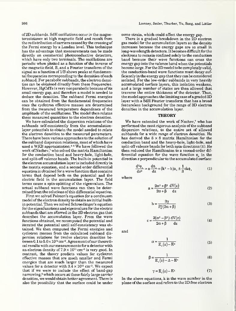
986 Lowney, Seller, Thurber, Yu, Song, and Littler
of2D subbands. SdH oscillations occxir in the magne-toresistance at high magnetic field and result fromthe redistribution ofcarriers caused by the crossing of
the Fermi energy by a Landau level. This technique
has the advantage that measurements can be madedirectly on commercial photoconductive detectors,
which have only two terminals. The oscillations are
periodic when plotted as a function of the inverse of
the magnetic field, B, and a Fourier transform of the
signal as a function of LIB shows peaks at fundamen-tal frequencies corresponding to the densities ofeachsubband. For parabolic subbands, the electron densi-
ties can be obtained directly from these frequencies.
However, HgCdTe is very nonparabolic because ofits
small energy gap, and therefore a model is needed to
deduce the densities. The subband Fermi energies
can be obtained from the fundamental frequencies
once the cyclotron effective masses are determinedfrom the measured temperature dependence of the
amplitude of the oscillations. The model then relates
these measured quantities to the electron densities.
We have calculated the dispersion relations of the
subbcinds self-consistently from the accumulation-layer potentials to obtain the model needed to relate
the electron densities to the measured parameters.There have been various approaches to the solution of
the subband dispersion relations, most ofwhich haveused a WKB approximation.'*-^ We have followed the
work ofNachev,' who solved the matrix Hamiltonianfor the conduction band axid heavy-hole, light-hole,
and split-off valence bands. The built-in potential in
the electron accumulation layer is included directly in
the matrix equation, and a second order differential
equation is obtained for a wave function that contains
terms that depend both on the potential and the
electric field in the accimiulation layer. The field
terms cause a spin-splitting of the eigenvalues. Theactual subband wave functions can then be deter-
mined from the solutions ofthis differential equation.
First we solved Poisson's equation for a continuummodel ofthe electron density to obtain an initial built-
in potential. Then we solved Schroedinger's equationfor the eigenfunctions and eigenvalues for the electric
subbands that are allowed in the 2D electron gas thatdescribes the accumulation layer. From the wavefunctions obtained, we recomputed the potential anditerated the potential imtil self-consistency was ob-
tained. We then computed the Fermi energies andcyclotron masses from the calculated subband dis-
persion relations for twelve electron densities be-
tween 0. 1 to 5.0 X 10^2 cm-2. Agreement ofour theoreti-
cal results with our measurements for a detector withan electron density of 7.9 x 10^^ cm-^ is very good. In
contrast, the theory predicts values for cyclotron
effective masses that are much smaller and Fermienergies that £ire much larger than the measuredvalues for a detector with 3.4 x 10^^ cm^^. We expect
that if we were to include the effect of band-gapnarrowing,* which occurs at these fairly large carrier
densities, we would obtain better agreement. There is
also the possibility that the surface could be imder
some strain, which could affect the energy gap.
There is a gradual breakdown in the 2D electron
gas model for the accumulation layers as the density
increases because the energy gaps are so small in
long-wavelength detectors. Itbecomes difficult for theelectrons to remain confined solely to the conductionband because their wave functions cam cross theenergy gap into the valence band when the potentials
become large. For the 2D model to be completely valid,
the conduction-band wave functions must decay suf-
ficiently in the energy gap that they can be consideredisolated. For the low-order subbands in very heavily
accumulated surface layers, this isolation weakens,and a large number of states are then allowed that
traverse the entire thickness of the detector. Thus,the model approaches the limiting case ofa graded 3Dlayer with a SdH Fourier transform that has a broadfeatureless background for the range of 3D electron
densities in the accumulation layer.
THEORYWe have extended the work of Nachev,^ who has
performed the most rigorous analysis of the subbanddispersion relations, to the entire set of allowed
subbands for a wide range of electron densities. Hehas derived the 8x8 matrix Hamiltonian for the
conduction band and the heavy-hole, light-hole, andsplit-offvalence bands for both spin directions (±). Hethen reduced the Hamiltonian to a second-order dif-
ferential equation for the wave function<t)^.
in the
direction z perpendicular to the accumulated surface:
where
a =2a^ + dV(z)
2a + p dz
b = 3y
c =
Po^(2a + P)
3(a^-p^)dV(z)
2a-i-p dz
and
a =E,(z)-E*
1
Ejz)-A-E*
y = E,(z)-E*
(1)
(2)
(3)
(4)
(5)
(6)
(7)
In the above equations, k is the wave number in the
plane ofthe surface and refers to the 2D free electron
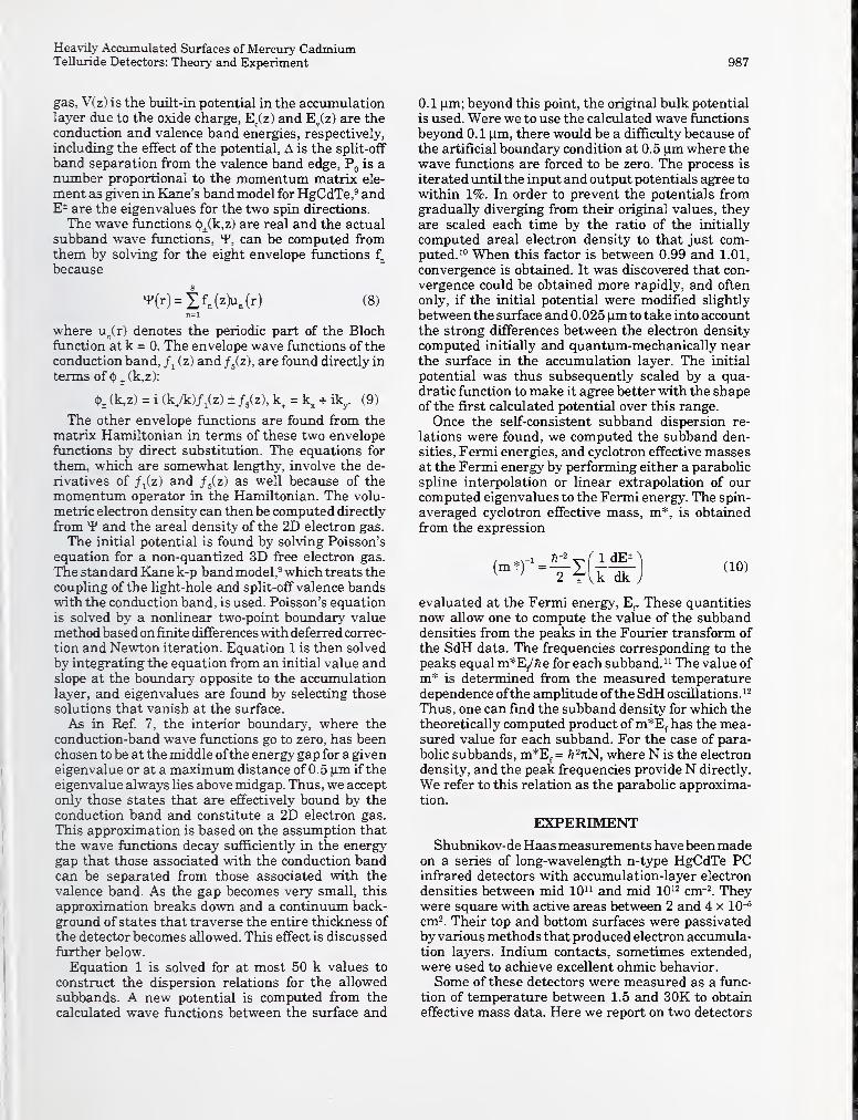
Heavily Accumulated Surfaces of Mercury CadmiumTeUuride Detectors: Theory and Experiment 987
gas, V(z) is the built-in potential in the accumulationlayer due to the oxide charge, E^(z) and E^(z) are theconduction and valence band energies, respectively,
including the effect of the potential, A is the spht-off
band separation from the valence band edge, is anumber proportional to the momentimi matrix ele-
ment as given in Kane's band model for HgCdTe,^ andE- are the eigenvalues for the two spin directions.
The wave functions <t)^(k,z) are real and the actual
subband wave functions, can be computed fromthem by solving for the eight envelope functions f^^
because
^(r) = if.(zK(r) (8)n=l
where u_^(r) denotes the periodic part of the Blochfunction at k = 0. The envelope wave functions of the
conduction band, /Jzj and j-iz), are foimd directly in
terms of ({) . (k,z):
(!)^ (k,z) = i (k /k)/,(z) ± /^(z), k^ = k + ik„. (9)
The other envelope functions are found from the
matrix Hamiltonian in terms of these two envelope
functions by direct substitution. The equations for
them, which are somewhat lengthy, involve the de-
rivatives of /j(zj and /.(z) as well because of the
momentimi operator in the Hamiltonian. The volu-
metric electron densit>' can then be computed directly
from ^ and the areal density of the 2D electron gas.
The initial potential is found by solving Poisson's
equation for a non-quantized 3D free electron gas.
The standard Kane k-p band model,^ which treats the
coupUng of the light-hole and split-off valence bandswith the conduction band, is used. Poisson's equationis solved by a nonlinear two-point boimdary value
method based on finite differences with deferred correc-tion and Newton iteration. Equation 1 is then solved
by integrating the equation from an initial value andslope at the boimdary opposite to the accumvdationlayer, and eigenvalues are found by selecting those
solutions that vanish at the surface.
As in Ref 7, the interior boundary, where the
conduction-band wave functions go to zero, has beenchosen to be at the middle ofthe energy gap for a given
eigenvalue or at a maximum distance of 0.5 |im if the
eigenvalue always hes above midgap. Thus, we accept
only those states that are effectively bound by the
conduction band and constitute a 2D electron gas.
This approximation is based on the assumption that
the wave functions decay sufficiently in the energygap that those associated with the conduction bandcan be separated from those associated with the
valence band. As the gap becomes very small, this
approximation breaks down and a continuimi back-
ground of states that traverse the entire thickness of
the detector becomes allowed. This effect is discussed
further below.
Equation 1 is solved for at most 50 k values to
construct the dispersion relations for the allowed
subbands. A new potential is computed from the
calculated wave functions between the surface and
0.1 |a.m; beyond this point, the original bulk potential
is used. Were we to use the calculated wave functions
beyond 0.1 |j.m, there would be a difficulty because of
the artificial boundary condition at 0.5 |im where thewave functions are forced to be zero. The process is
iterated vmtil the input and output potentials agree to
within 1%. In order to prevent the potentials fromgradually diverging from their original values, theyare scaled each time by the ratio of the initially
computed areal electron density to that just com-puted.^" When this factor is between 0.99 and 1.01,
convergence is obtained. It was discovered that con-
vergence could be obtained more rapidly, and often
only, if the initial potential were modified slightly
between the surface and 0.025 p.m to take into account
the strong differences between the electron density
computed initially and quantiun-mechanically nearthe surface in the accumulation layer. The initial
potential was thus subsequently scaled by a qua-dratic function to make it agree better with the shapeof the first calculated potential over this range.
Once the self-consistent subband dispersion re-
lations were foimd, we computed the subband den-
sities, Fermi energies, and cyclotron effective massesat the Fermi energy by performing either a parabolic
spline interpolation or linear extrapolation of ourcomputed eigenvalues to the Fermi energy. The spin-
averaged cyclotron effective mass, m*, is obtained
from the expression
(10)
evaluated at the Fermi energy, E^ These quantities
now allow one to compute the value of the subbanddensities from the peaks in the Fourier transform of
the SdH data. The frequencies corresponding to the
peaks equal m*E//2 e for each subband. The value of
m* is determined from the measured temperaturedependence ofthe ampUtude ofthe SdH oscillations.^^
Thus, one can find the subband density for which the
theoretically computed product ofm*Ef has the mea-sured value for each subband. For the case of para-
bolic subbands, m*Ef = ^^nN, where N is the electron
density, and the peak frequencies provide N directly.
We refer to this relation as the parabolic approxima-tion.
EXPERIMENTShubnikov-de Haas measurements have beenmade
on a series of long-wavelength n-t3T3e HgCdTe PCinfrared detectors with accumulation-layer electron
densities between mid lO^^ and mid 10^^ cm-^. Theywere square with active areas between 2 and 4 x 10"*
cm^. Their top and bottom surfaces were passivated
by various methods that produced electron accumula-tion layers. Indium contacts, sometimes extended,
were used to achieve excellent ohmic behavior.
Some of these detectors were measured as a func-
tion of temperature between 1.5 and 30K to obtain
effective mass data. Here we report on two detectors

988 Lowney, Seller, Thurber, Yu, Song, and Littler
ENERGY BAND DIAGRAM CONTINUUM AND QUANTUM SOLUTIONS
-250 -
-300
INTERFACE
0.05 0.1
POSITION ifim)
0.15
15
a
2 10
CONTINUUM
QUANTUM
0.025 0.05 0.075
POSITION (^m)
0.1
SUBBAND DISPERSION RELATIONS SUBBAND POPULATIONS
-80
-- SPIN DOWN
— SPIN UP
I'
I
'
0.05 0.1
WAVENUMBER (nm"')
0.15 0.2
Fig. 1 .(a) Built-in potential for accumulation layer with total electron
density of 8.9 x 10" cm-^ and alloy fraction x = 0.191. The horizontal
lines are the subband-edge energies for the first three subbands (n =
0,1,2). (b) Dispersion relations for the subbands for this potential,
showing spin-splitting. The curves are labeled by subband numberfrom 0 to 6.
TOTAL DENSITY (lO'^cm"')
Fig. 2. (a) Electron density computed by solving Poisson's equation for
a charge continuum (dashed) and from full quantum-mechanicalcalculation (solid) for case of Fig. 1 . (b) Suband densities as a function
of total density. Lines are linear least-squares fit. The curves are
labeled by subband number from 0 to 3, and x = 0.1 91
.
that have had extensive measurements made onthem. Ac magnetic-field modulation and lock-in am-plifier techniques that use the second harmonic detec-
tion were used to obtain the signal for magnetic fields
up to 12 The SdH oscillations are a small percent-
age ofthe total magnetoresistance, and ac techniques
significantly enhance the measured SdH oscillations
in these detectors.
Excellent signal-to-noise ratios were obtained in
most detectors even at temperatures as high as 30K.Measurements made at 30, 60, and 90 degree rota-
tions of the sample about the perpendicular to the
surface showed that the peak frequencies varied as 1/
cos(9), where 9 is the rotation angle, as expected for a
2D electron gas.
RESULTS AND DISCUSSION
Calculations of the subband dispersion relations
and related quantities have been made for the rangeof areal electron densities between 0.1 and 5.0 x 10^^
cm"^. The x-value of the detector was taken to be0. 191, with a corresponding energy gap of41. 1 meV,^^
which is representative of long-wavelength detectors
and equal to that ofthe detectors we report on below.
The background electron doping densitywas assumedto be 3.9 X 10^* cm-^, which was reported for these
detectors, along with a bulk mobility of 2.5 x 10^ cmVVs at 77K. Bulk SdH oscillations were not observed
because of their low frequency, which implies that
they would have been observed only at low magnetic
Heavily Accunmlated Surfaces of Mercury CadmiumTelluride Detectors: Theory and Experiment 989
fields where broadening effects greatly reduce their
signal strength. The temperature is taken to be 6K, at
which the material is degenerate. As an example, the
built-in field and subband dispersion relations for anareal density of 8.9 x 10^^ cm*- are shown in Figs, la
and lb, respectively. The siirface potential in Fig. lais about three times greater than the energy of the
lowest subband edge and over five times the energygap. The spin splitting is evident in Fig. lb, and is
greatest for the lowest subband. The density of elec-
trons in the spin-up subband is about 15% greater
than in the spin-down subband for the lowest four
subbands. At the lower densities, this percentage
decreases somewhat, especially for the higher sub-
bands, while at higher densities it remains nearly the
same for all subbands. Note also that the deviation
fi-om a parabolic to a nearly linear dependence ofE onk IS clear for energies only about 10 meV above the
subband edges. The small oscillations in these curves
are due to 1% numerical uncertainty in the solutions.
The corresponding electron density in the ac-
cumulation layer is shown in Fig. 2a for both the semi-
classical result from the initial solution of Poisson's
equation and the final quantum-mechanical result
fi"om the subbands. The width of the accumulationlayer is seen to be about 0.1 jam. The latter density is
greatly reduced at the surface because of the bound-ary condition on the wave functions. It goes to zero
discontinously across the boiindary because of the
dependence ofthe wave function on the derivatives of
/j and /j, which undergo a discontinuous change froma finite to zero value at the boundary. Therefore the
shape ofthe potential near the interface is different in
the two cases, and the value of electron density
obtEiined quantum-mechanically is less than that of
the initial semiclassical solution. The electron densi-
ties ofthe first four subbands are plotted as a function
of total density in Fig. 2b. We compute the total
density from a sum over only the first four subbands,
for which we can perform accurate computations. Weestimate the error incurred by this approximation to
be less than 1%. The relations are nearly Hnear withaverage slopes of0.673, 0.223, 0.077, and 0.027 for the
first (n = 0) through fourth (n = 3) subband, respec-
tively. The deviations from linearity are less than 1%.
These values differ somewhat from our correspondingexperimental values of0.609, 0.258, 0. 101, and 0.032,
which have deviations from linearity of only a fewpercent, although the experimental values may not be
completely accxirate because they are based on the
parabolic approximation for the density in the SdHanalysis. This near linearity shows that the shape of
the potential distribution is relatively insensititve to
the magnitude ofthe surface potential. The difference
between theoretical and experimental slopes mayindicate that the potential distribution is somewhatdistorted, which can be caused by strain or band gapnarrowing.The subband Fermi energies and cyclotron effective
masses are shown in Figs. 3a and 3b, respectively, as
a function of total density. The Fermi energy in the
bulk is computed to be 5.44 meV for an assumed bulk
density of 3.9 x 10" cm-^. The scatter in the massvalues is due to the derivative in Eq. 10. Although the
calculated eigenvalues appear relatively smooth in
Fig. lb they are only accurate to about 1%, and this
uncertainty as well as that due to the discreteness of
the k-values causes the theoretical masses to haveerrors ofabout 5% occasionally. A more refined calcu-
lation would lead to better accuracy. The strong
variations of the masses with density attest to the
nonparabolicity of the dispersion relations, whichhave an effect on the optimization of device perfor-
mance. The serpentine shape of the curves is due to
the strong curvature of the built-in potential.
We have made SdH measurements on a number of
FERMI ENERGIES
200
12 3 4
TOTAL DENSITY {iC'cm"')
CYCLOTRON EFFECTIVE MASSES
0.05
0.04 -
0.03
0.02 -
0.01
y0 0
^ 1
B 2
B 3
b
TOTAL DENSITY (10"cm'')
Fig. 3. (a) Subband Fermi energies as a function of total density,
measured from the bottom of each subband. (b) Ratio of subbandcyclotron effective masses to the electron mass at the Fermi energy as
a function of total density. Lines are cubic least-squares fit. The curves
are labeled by subband number from 0 to 3, and x = 0.191
.
990 Lowney, Seller, Thurber, Yu, Song, and Littler
FOURIER TRANSFORM OF SHUBNIKOV-DE HAAS DATA
0 10 20 30 40
FREQUENCY (T)
a
FOURIER TRANSFORM OF SHUBNIKOV-DE HAAS DATA
,FREQUENCY (T)
b
Fig. 4. (a) Fourier transform of SdH data at 5K for Sample 1 ; the label
"h" stands for harmonic; peaks are labeled by subband number, (b)
Same for Sample 2, except at 2K. Actual SdH data for the signals as
a function of magnetic field are given in insets and x = 0.191.
long-wavelength, commercial, n-t3rpe PC detectors
with total densities between 5 x 10" and 5 x 10^^ cm-^.
The SdH Fourier transforms of two different repre-
sentative detectors are shown in Figs. 4a and 4b alongwith the actual SdH data, which show the oscillations
vs magnetic field. The notations ' and " refer to
different surfaces or to different regions on the samesurface since both surfaces ofthe detector were passi-
vated. The detector in Fig. 4a was passivated with the
usual anodic oxidation process, ^ while that in Fig. 4bwas passivated by a different method. The separa-
tions of peaks due to spin-splitting are predicted byour theory to be about half of that we observed, andthus we expect that these multiple peaks are due to
different surface densities. The splittings vary some-what from detector to detector as well. Thus, the effect
of spin spUtting is just to broaden each peak. The
transform corresponding to the detector with lowertotal density, Sample 1, in Fig. 4a, has clear, strong
peaks, while that for the one with higher density,
Sample 2, in Fig. 4b, has peaks that rise less above thebackground. One reason is that the penetration oftheenergy gap by the wave functions is much greater for
the heavily accumulated case, especially for the low-
est subband. There is a mixture of subband states
bound to the conduction bcind and continuum states
that traverse the entire detector. Thus, the layer of
electron accumulation is not well described by a
simple 2D electron gas at high densities and smallenergy gaps. The Fourier transform for a heavily
accumulated, narrow gap detector can have a broadbackground of contributions from the range of 3Dstates corresponding to the graded 3D electron den-
sity in the accumulation layer. The 2D states, whichare bound to the conduction band, appear as well in
the Fourier transform and rise above the backgroundbecause they contribute at only one frequency for eachsubband. The complexity ofthe background signature
in Fig. 4b may indicate that there is nonuniformity in
the surface density as well because ofthe two surfaces
and multiple regions within a surface. Even thoughthe relative ampUtude of the oscillations of Sample 2
was almost ten times smaller than that of Sample 1,
the Fourier transform successfully resolved the sig-
nature of the detector.
We have computed the subband electron densities
from the measured cyclotron effective masses andFermi energies for these two detectors. The results
from the two surfaces were averaged because wecould not resolve the sphtting at higher tempera-tures. For sample 1, the measured data are: m^ =
0.022 ± 0.001, E° = 79 ± 4 meV, m; = 0.014 ± 0.001, andEji = 42 ± 3 meV. The corresponding theoretical valueswere obtained by finding the total density for whichthe m*Ef values for the subbands best agreed withexperiment: m; = 0.023 ± 0.001, E? = 75 ± 2 meV, m;= 0.015 ± 0.001, and E
J= 38 ± meV. The predicted total
density is found to be 7.9 x 10" cm-^, which is consid-
erably less than the value of 1.2 x 10^^ cm-^ that is
obtained from the parabolic approximation for the
density. The agreement between theory and ex-
periment is vdthin the assigned uncertainty vidth the
theoretical values for the effective masses slightly
larger than measured. Thus, we expect that the en-
ergy gap may be smaller than the one we are using.
This may occur because ofband-gap narrowing, whichoccurs at high densities because of the many-bodyinteractions between electrons. We estimate the band-
gap reduction to be at most 10% at this density.^ ForSample 2, we report the results for the peaks labeled
with " because the unprimed peaks were above our
calculated densities, and some of the single-primed
peaks were not as well separated from the back-
ground. We do not report the n = 2 and n = 3 peaksbecause they are also not very well separated. Themeasured data for the peaks labeled with " are: m* =
0.020, E? = 312 meV, m; = 0.010, and EJ= 277 meV.The uncertainties for these nimibers are about 20%.
Heavily Acciomulated Surfaces of Mercury CadmiumTelluride Detectors: Theory and Experiment 991
We obtain from the total density that gives best
agreement between our theory and the measuredsubband m*Ef values: m; = 0.039 ± 0.002, E? = 160 ±3 meV, m; = 0.029 ± 0.001, and E} = 80 ±2 meV. Thepredicted total density is then found to be 3.4 x lO^^
cm-2, which is also considerably less than the value of
4.3 X 10^2 cm-2 from the parabolic approximation.
However, Sample 2, which was made by a different
process from the traditional anodic oxidation method^thatwas used for Sample 1, disagrees with the predic-
tions, because the measured masses are so muchsmaller and the Fermi energies so much larger thanthe predicted values. Band-gap narrowing would be
larger for these samples, probably in excess of 10% of
the energy gap, and the gap could become very small.
However, much more work is needed to understandthe cause of this disagreement, which may involve
strain as well. The relatively large Fermi energies
and small masses could imply that the built-in poten-
tial is more like a square well in these detectors with
heavy accumulation.
CONCLUSIONSThe dispersion relations for all the 2D subbands in
the accimiulation layers of HgCdTe detectors have
been computed by solving the 8x8 matrix Hamilto-
nian for a large range of electron densities (0.1 to 5 x
10^- cm-2). The subband densities, Fermi energies,
and cyclotron effective masses have been computed as
a function of the total electron density. The results
show strong nonparabolicity and a breakdown in the
simple 2D model of the electron gas at high densities
and small energy gaps. The near linear dependence of
the subband densities on total density, which has
been observed experimentally, has been confirmed
theoretically. The agreement of our calciilations with
experiment is good at the lower densities and maypossibly be improved by inclusion ofthe effect ofband-
gap narrowing. At the liigher densities differences are
large, and further work including the effects ofband-
gap narrowing and strain is needed to understand the
measurements. Models such as these provide a basis
to characterize the electron states in the accumula-
tion layers of these detectors, which have a large
effect on device performance.
The direct application of these results to the char-
acterization of detectors is not simple, however. Theproperties ofthe accumulation layers constitute only
one ofthe contro.lling factors in detector performance.
Others include the bulk electrical and optical proper-
ties, the type and quality ofthe contacts and packag-
ing, and the effects from the method ofdelineating the
detectors, such as ion milling. The contribution ofthis
work has been to present a direct, two-terminal mea-surement that can be used to determine the electron
density of the accumulation layers of a detector.
Failure to have sufficient accumulation can lead to
increased surface recombination and degradation of
detectivity. Excessive accumulation, on the otherhand,
can lead to a large shimt conductance, which also can
degrade detectivity. Thus, one can use this method to
study the dependence of detectivity on the method of
passivation and the resiilting level of accumulation.
The optimum process can be determined, and subse-
quently this method C£in be used to monitor the
accvmiulation layers during manvifacturing and to
monitor their stabiHty as a function of time.
REFERENCES1. Y. Nemirovsky and G. Bahir, J. Vac. Sci. Technol. A7, 450
(1989).
2. Y. Nemirovsky and I. Kidron, Solid-State Electron. 22, 831
(1979).
3. R.J. Nicholas, F. Nasir and J. Singleton, J. Cryst. Growth 86,
656(1988).
4. W. Zawadzki. J. Phys. C 16, 229 (1983).
5. Y. Takada, J. Phys. Soc. Jpn. 50, 1998 (1981).
6. G. Nachtwei, P. Schulze, G. Gobsch, G. Paasch, W. Kraak, H.
Kruger, and R. Herrmann, Phys. Status Solidi b 148, 349
(1988) .
7. I. Nachev, Semicond. Sci. Technol. 3, 29 (1988).
8. G. Trankle, E. Lach, A. Forchel, C. Ell, H. Haug, G. Weimann,G. Griffiths, H. Kroemer, and S. Subbanna, J. de Phys. Coll.
€5,48,385(1987).9. E. Kane, J. Phys. Chem. Solids 1, 249 (1957).
10. J. Sune, P. Olivo and B. Ricco, J. Appl. Phys. 70, 337 (1991).
11. S. Yamada, H. Asai and Y. Kawamura, J. Appl. Phys. 72, 569
(1992).
12. D.G. Seller, G.B. Ward, R.J. Justice, R. J. Koestner, M. W.Goodwin, M. A. Kinch and J. R. Meyer, J. Appl. Phys. 66, 303
(1989) .
13. D.G. Seller, J.R. Lowney, C.L. Littler and M. R. Loloee, J. Vac.
Sci. Technol. A8, 1237 (1990).

APPENDIX BS€micond. Sci. Technol. 8 (1993) 888-910. Printed in the UK
INVITED PAPER
Review of semiconductor microelectronic
test structures with applications to
infrared detector materials and processes'^
J J Kopanski and C E Schuster
Semiconductor Electronics Division, National Institute of Standards andTechnology, Gaithersburg, MD 20899, USA
Abstract. The impact of microelectronic test structures, as they have been applied
to silicon integrated circuits (ics) and gallium arsenide monolithic microwaveintegrated circuits (mmics), is reviewed. General principles for the use of test
structures with possible applications to infrared (iR) detector technology based onHgCdTe and other materials are emphasized. The uses of test structures for Si
and GaAs, test chip design methodology and some examples of how test
structures have been applied for process control and to increase yield are
discussed. Specific test structures and techniques that have been applied to ir
detectors are also reviewed The basic design considerations and measurementspossible with each class of test structure are discussed. The important experience
of the Si and GaAs industries, applicable to ir detectors, is that significant yield
improvement is possible with improved process control using test structures.
Increased research efforts to expand the applications of test structures to ir
detector manufacture are indicated.
1. Introduction
Since the mid-1970s, the National Institute of Standards
and Technology has engaged in a programme to develop
well characterized test structures, test methods and data
analysis techniques for use by the semiconductor
manufacturing industry. Test structures are micro-
electronic devices that are fabricated by the same
processes used to manufacture semiconductor integrated
circuit products, and that are used to measure selected
material, process or tool parameters by means of
electrical tests. Properly designed test structures can be
used to evaluate semiconductor materials, to determine
and monitor process centring parameters, to measure
critical device and circuit parameters (which can be input
to device models), to identify and quantify yield-limiting
defects and to assess processing tool performance.
As they are used today, test structures are indispens-
able to the successful process development and manu-
facture of Si and GaAs devices and circuits. The use of
test chips speeds up process development, product
fabrication and test, and enhances the reliability of the
product—all at decreased cost. The use of test structures
as part of a comprehensive test programme can ensure
that performance and reliability have been built into
circuits. The prominence of test structures is the result
* Contribution of the National Institute of Standards andTechnology; not subject to copyright.
of many years of experience with their use in the
manufacture of silicon ics and, more recently, GaAsMMICS.
The next section contains a tutorial describing howtest structures have been applied to silicon ics and GaAsMMICS. It is the intention of this tutorial to encourage
greater acceptance and use of test structures in ir detector
manufacture by developing an understanding of the ways
test structures have had an impact on the larger silicon
and GaAs industries. Elements of a hierarchical test chip
design methodology, which maximizes the impact of
using test structures, are described. This bottom-up
approach to test chip design provides a blueprint for
applying test structures to any semiconductor device
fabrication process. On the basis of experience with
silicon and GaAs test structures, a guide to selecting the
appropriate kind and number of test structures, as well
as principles for effective application of these devices, is
provided. Three examples of how test structures have
been applied for process control and to increase yield are
included. The first two examples are from Si technology
and illustrate process/tool control using the analysis of
results of measurements on test structures. The third
example describes how test structures suggested an
improvement of an etch process for GaAs mmic fabrica-
tion and illustrates the importance of using a high area
density of test structures early in process development.
In the third section, the current use of test structures
and specialized measurements most commonly applied
0268-1242/93/060888 + 23 $07.50 © 1993 lOP Publishing Ltd
Review of test structures for infrared detectors
to IR detector devices, processes and materials are
discussed. The characterization concerns of ir detectors
are compared and contrasted with Si and GaAs circuits.
Design considerations and the uses of each test structure
are discussed. The section is meant to be a comprehensive
listing of devices that are well described in the literature
and that are thus candidates for inclusion in ir detector
test chips.
The final section contains a discussion of specific test
structures and principles for the expanded application of
test structures which have the potential for enhancing ir
detector technology. Areas where further study is needed
are outlined. Relevant principles from the current body
of test structure experience are used to suggest changes
in practices that could ultimately affect the manu-facturability of ir detectors.
2. Using test structures effectively
This section summanzes test structure utilization from a
Si and GaAs perspective, but with the goal of featuring
ideas which should also be applicable to the ir detector
industry. First, some selected applications and imple-
mentations of test structures are presented to illustrate
why and how test structures can be used. Then, a
discussion of test structure methodology explains howto develop successful test structure implementations.
FinaUy, case studies from the Si and GaAs industries are
used to show how three types of problem, potentially
applicable to ir detector manufacturing, were discovered
and solved using test structures.
2.1. Why test structures are used
Test structures provide a means for obtaining parameters
that can be used to diagnose, monitor and predict the
performance of the fabrication process, the products
manufactured and the manufacturing equipment. Test
structure data can be used to estabhsh, improve or ensure
process control and product yield. The results of test
structure data analysis may be used as feedback to the
manufacturing process or as the basis for future
development work.
Test structure data can be collected rapidly using a
computer-controlled probe station. This enables manysamples of many types of parameters to be collected
during processing without a significant impact on
manufacturing time. Test structure measurements also
enable users to derive parameters that cannot be obtained
at all, or as economically, from other forms of testing. If
the collected data are efficiently reduced and evaluated,
processing and yield-limiting problems can be detected
and solved promptly, improving the economics of the
manufacturing process.
Test structures can be applied to processes, pro-
ducts and process tools throughout the manufacturing
lifecycle—in development, production, technology trans-
fer and buying and selling. The following discussion
describes some typical uses of test structures during these
times.
During developmental phases, process control and
adequate yields must be established for successful
production of products. Collected test structure data are
evaluated to identify critical factors in the various process
steps that must be controlled and to detect problems that
Hmit product yield. When diagnosing control and
yield-limiting problems, the user may also correlate
collected data with historical or simulated data. Collected
data can also be used as input to modelling studies used
in extended developmental evaluations, such as newprocess development, device and circuit modelling and
logic and fault simulation.
During development and production, after process
control and adequate yields have been achieved, test
structures can be used to monitor the critical parameters.
Collected test structure data are compared with data
from previously verified lots to ensure that process
control is maintained. For a well controlled and well
characterized process, test structure data can also be
evaluated to determine if existing correlations can be used
to reduce the set of test structures needed to monitor the
process.
In efl"orts involving technology transfer, comparison
of test structure data between participants is useful for
verifying that the desired performance criteria are
successfully met on all manufacturing lines. This is
important in developing multiple sources for materials,
processes and products and in demonstrating the
applicabihty of new processing tools.
When buying and selling, performance criteria
derived from test structures can be used as manufacturing
sp>ecifications. Such specifications help the seller to
market products and services and enable buyers to makecomparisons when selecting materials, processes, devices,
circuits and processing tools.
Test structures to support these applications can be
categorized into several classes according to their general
purpose: to extract material, process, device or circuit
parameters; to detect or quantify random faults and
processing defects; to establish product reliability and
yield; to formulate layout design rules; and to assess
processing tool performance. The remainder of section
2.1 discusses typical user goals that can be achieved, and
the test structures, parameters and types of analysis
required. It also provides references for further reading.
The reader should note that, in many cases, the references
(and their references) reveal assumptions, limitations or
requirements which are beyond the scope of this
discussion.
2.1.1. Test structures to extract material, process, device
and circuit parameters. Material, process, device and
circuit parameters are either directly measured or
indirectly extracted from test structures. These characteri-
zation parameters are then compared and correlated to
diagnose and monitor processes or products. Characteri-
zation parameters can also be used to build models for
software simulation of processes, devices or circuits
889

J J Kopanski and C E Schuster
[1, 2]. Such simulations provide results which can be
used in evaluations to diagnose existing process prob-
lems, develop process enhancements or future processes,
determine target and tolerance values or layout rules, or
design devices and circuits. The discussion below
identifies the major characterization parameters and test
structures used to characterize materials, processes,
devices and circuits.
Materials. Test structures can be used to determine
properties of starting materials, surface and interfacial
regions, ion-implanted layers and deposited films. Here,
test structures provide an efficient and economical means
of measuring parameters that are otherwise impossible
or difficult to obtain, such as those requiring advanced
physical analysis techniques. Evaluation and diagnosis
of materials parameters are used to ensure the uniformi-
ties needed to support manufacture of functioning
devices, as they may correlate with performance factors
[3] or device quality [4, 5]. Since materials parameters
are obtained early in the processing, correlations with
other test structure parameters are timely indicators for
monitoring and predicting product performance.
To determine starting material parameters associated
with deep-level defects, an integrated gated-diode electro-
meter is used [6, 7]. This test structure consists of a
gated-diode with a preamplifier and is used to measure
leakage current, from which both carrier lifetime and
surface recombination velocity can be extracted by using
an equivalent circuit model. Information related to
impurity concentration in the material is determined
using a Hall structure for the Hall mobility and a long
gate-length transistor for the drift mobihty [8].
For ion-implanted layers, test structures are used to
determine the doping profile and information about
residual substrate impurities [4]. The dopant density and
depletion width can be determined using transistors,
capacitors or diodes [9]. These structures also allow C-Vprofihng to be done, which indicates further information
about drift mobility, the presence of traps, activation
energy, carrier concentration, ideality factor and barrier
height [5, 10].
Parameters such as conductivity and contact resist-
ance are sometimes considered as measures of material
quality [8, II], but are more accurately measures of
process quahty [12]. Regardless of this, these parameters
are critical to making good Hall measurements [II] and
must be evaluated when making Hall measurements. Test
structures and references for conductivity and contact
resistance measurements are found in the following
section.
Processes. Process parameter test structures provide
information about layer uniformity, layer interface
conditions and feature definition resulting from the
various process steps. These parameters are important
for making correlations related to monitoring, diagnosing
and predicting process and process tool performance. The
test structures most frequently used to provide process
parameters include van der Pauw sheet resistors.
cross-bridge sheet resistors, interfacial contact resistors,
potentiometric alignment structures, transistors, capaci-
tors and diodes.
The van der Pauw sheet resistor, cross-bridge sheet
resistor, interfacial contact resistor and potentiometric
ahgnment structure are implemented in each of the
process layers where uniformity or particular target
values are critical. The van der Pauw sheet resistor
measures conductivity [4, 13-15]. The interfacial contact
resistor provides the interfacial contact resistance, which
is used to evaluate the quality of the contact formation
process [16-18]. A cross-bridge sheet resistor [14, 15,
19-21], which provides sheet resistance and allows
extraction of Hnewidth, is used to evaluate the quahty of
film deposition processes. The potentiometric alignment
structure [22, 23] provides a measure of the misregistra-
tion of photomask features between two conducting
layers. Alignment structures are also used to indicate
process tool performance (see section 2.1.5) and to
formulate or evaluate geometric layout rules (see section
2.1.4).
Transistor, capacitor and diode structures provide
information about processing, as well as materials. For
example, threshold voltage data from transistor-based
test structures have been correlated with sheet resistance
data to diagnose contamination problems [24]. Thresh-
old voltage data have also been used to infer parameters,
such as dopant concentration, for which no direct
measurement method exists, as described in section 2.4.1.
Other process parameters commonly measured are oxide
thickness using capacitors, and leakage currents using
diodes.
Devices. Test structures for characterizing device para-
meters are useful in process control and simulation. Like
process parameters, device parameters can be indicators
of process quahty or product yield, as demonstrated in
section 2.4.2. Device parameters also frequently correlate
with other test structure data. Test structures for
characterizing devices include transistors, diodes, resis-
tors and capacitors that have the same layouts, operating
conditions and measurement conditions as the devices
used to construct the ic product. This allows meaningful
comparison and correlation for monitoring, diagnosing
or predicting product performance. Such test structures
can also be used to develop specifications for designers,
buyers and sellers.
Parameters typically measured from field effect
transistors include threshold or pinch-off voltage, satura-
tion voltage, breakdown voltage, leakage current, trans-
conductance, parasitics associated with device terminals
and any other parameters needed for equivalent circuit
models [12, 25]. Many of these parameters can be
extracted from diodes as well. Information needed by a
circuit designer to interconnect devices and assess loading
conditions can be determined using resistance, capacit-
ance, delay and gain values measured from resistors,
capacitors and transistors.
Circuit elements. Circuit characterization test structures
890-
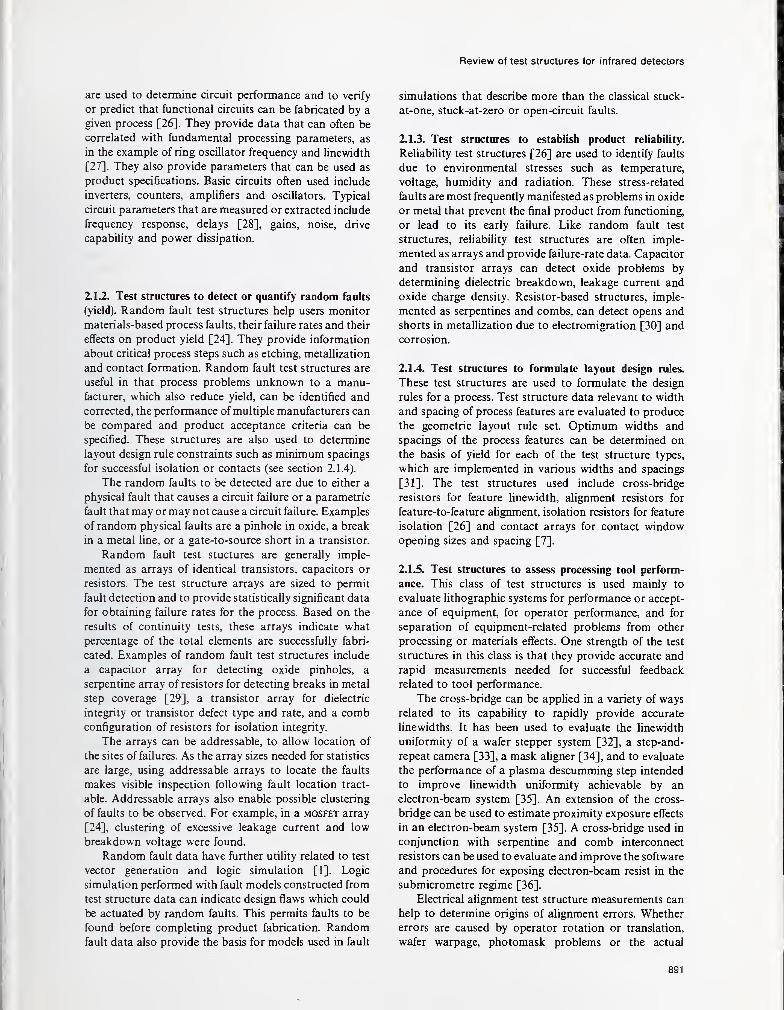
Review of test structures for infrared detectors
are used to determine circuit performance and to verify
or predict that functional circuits can be fabricated by a
given process [26]. They provide data that can often be
correlated with fundamental processing parameters, as
in the example of ring oscillator frequency and linewidth
[27]. They also provide parameters that can be used as
product specifications. Basic circuits often used include
inverters, counters, amphfiers and oscillators. Typical
circuit parameters that are measured or extracted include
frequency response, delays [28], gains, noise, drive
capability and power dissipation.
2.1.2. Test structures to detect or quantify random faults
(yield). Random fault test structures help users monitor
materials-based process faults, their failure rates and their
effects on product yield [24]. They provide information
about critical process steps such as etching, metallization
and contact formation. Random fault test structures are
useful in that process problems unknown to a manu-
facturer, which also reduce yield, can be identified and
corrected, the performance of multiple manufacturers can
be compared and product acceptance criteria can be
specified. These structures are also used to determine
layout design rule constraints such as minimum spacings
for successful isolation or contacts (see section 2.1.4).
The random faults to be detected are due to either a
physical fault that causes a circuit failure or a parametric
fault that may or may not cause a circuit failure. Examples
of random physical faults are a pinhole in oxide, a break
in a metal line, or a gate-to-source short in a transistor.
Random fault test stuctures are generally imple-
mented as arrays of identical transistors, capacitors or
resistors. The test structure arrays are sized to permit
fault detection and to provide statistically significant data
for obtaining failure rates for the process. Based on the
results of continuity tests, these arrays indicate what
percentage of the total elements are successfully fabri-
cated. Examples of random fault test structures include
a capacitor array for detecting oxide pinholes, a
serpentine array of resistors for detecting breaks in metal
step coverage [29], a transistor array for dielectric
integrity or transistor defect type and rate, and a combconfiguration of resistors for isolation integrity.
The arrays can be addressable, to allow location of
the sites of failures. As the array sizes needed for statistics
are large, using addressable arrays to locate the faults
makes visible mspection following fault location tract-
able. Addressable arrays also enable possible clustering
of faults to be observed. For example, in a mosfet array
[24], clustering of excessive leakage current and low
breakdown voltage were found.
Random fault data have further utility related to test
vector generation and logic simulation [1]. Logic
simulation performed with fault models constructed from
test structure data can indicate design flaws which could
be actuated by random faults. This permits faults to be
found before completing product fabrication. Randomfault data also provide the basis for models used in fault
simulations that describe more than the classical stuck-
at-one, stuck-at-zero or open-circuit faults.
2.1.3. Test structures to establish product reliability.
Reliability test structures [26] are used to identify faults
due to environmental stresses such as temperature,
voltage, humidity and radiation. These stress-related
faults are most frequently manifested as problems in oxide
or metal that prevent the final product from functioning,
or lead to its early failure. Like random fault test
structures, reliability test structures are often imple-
mented as arrays and provide failure-rate data. Capacitor
and transistor arrays can detect oxide problems by
determining dielectric breakdown, leakage current and
oxide charge density. Resistor-based structures, imple-
mented as serpentines and combs, can detect opens and
shorts in metallization due to electromigration [30] and
corrosion.
2.1.4. Test structures to formulate layout design rules.
These test structures are used to formulate the design
rules for a process. Test structure data relevant to width
and spacing of process features are evaluated to produce
the geometric layout rule set. Optimum widths and
spacings of the process features can be determined on
the basis of yield for each of the test structure types,
which are implemented in various widths and spacings
[31]. The test structures used include cross-bridge
resistors for feature linewidth, alignment resistors for
feature-to-feature ahgnment, isolation resistors for feature
isolation [26] and contact arrays for contact windowopening sizes and spacing [7].
2.1.5. Test structures to assess processing tool perform-
ance. This class of test structures is used mainly to
evaluate lithographic systems for performance or accept-
ance of equipment, for operator performance, and for
separation of equipment-related problems from other
processing or materials effects. One strength of the test
structures in this class is that they provide accurate and
rapid measurements needed for successful feedback
related to tool performance.
The cross-bridge can be applied in a variety of ways
related to its capability to rapidly provide accurate
Hnewidths. It has been used to evaluate the linewidth
uniformity of a wafer stepper system [32], a step-and-
repeat camera [33], a mask ahgner [34], and to evaluate
the performance of a plasma descumming step intended
to improve linewidth uniformity achievable by an
electron-beam system [35]. An extension of the cross-
bridge can be used to estimate proximity exposure effects
in an electron-beam system [35]. A cross-bridge used in
conjunction with serpentine and comb interconnect
resistors can be used to evaluate and improve the software
and procedures for exposing electron-beam resist in the
submicrometre regime [36].
Electrical alignment test structure measurements can
help to determine origins of alignment errors. Whether
errors are caused by operator rotation or translation,
wafer warpage, photomask problems or the actual
891
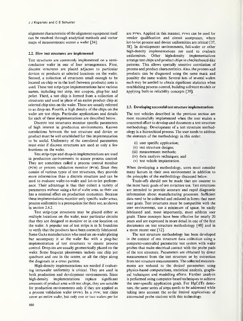
J J Kopanski and C E Schuster
alignment characteristic of the aHgnment equipment itself
can be resolved through analytical methods and vector
maps of measurements across a wafer [34].
2.2. How test structures are implemented
Test structures are commonly implemented on a semi-
conductor wafer in one of four arrangements. First,
discrete structures are placed adjacent to particular
devices or products at selected locations on the wafer.
Second, a collection of structures small enough to be
located on-chip or in the kerf (between products) area is
used. These test strip-type implementations have various
names, including test strip, test coupon, plug-bar and
pellet. Third, a test chip is formed from a collection of
structures and used in place of an entire product chip at
selected chip sites on the wafer. These are usually referred
to as drop-ms. Fourth, a high density of the chips on the
wafer are test chips. Particular applications and details
for each of these implementations are described below.
Discrete test structures monitor specific parameters
of high interest in production environments. Knowncorrelations between the test structure and device or
product must be well established for this implementation
to be useful. Uniformity of the correlated parameters
must exist if discrete structures are used at only a few
locations on the wafer.
Test strip-type and drop-in implementations are used
in production environments to assure process control.
They are sometimes called a process control monitor
(pcm) or process validation monitor (pvm). Since they
consist of various types of test structures, they provide
more information than a discrete structure and can be
used to evaluate wafer-to-wafer and lot-to-lot perform-
ance. Their advantage is that they collect a variety of
parameters without using a lot of wafer area, so their use
has a minimal effect on production economics. Because
these implementations monitor only specific wafer areas,
process uniformity is a prerequisite for their use, as shown
in section 2.4.2.
Test strip-type structures may be placed either at
multiple locations on the wafer, near particular circuits
that they are designed to monitor or in one location on
the wafer. A popular use of test strips is in Si foundries
to verify that the products have been correctly fabricated.
Some GaAs manufacturers who need an on-wafer plating
bar accompany it at the wafer flat with a plug-bar
implementation of test structures to ensure process
control. Drop-ins are usually geometrically placed on the
wafer. Some frequent placements include one chip per
quadrant and one in the centre, or all the chips along
the diagonals in a cross pattern.
High-density implementations are needed if evaluat-
ing intrawafer uniformity is critical. They are used in
both production and development environments. Since
high-density implementations replace significant
amounts of product area with test chips, they are suitable
for production environments only if they are applied as
a process validation wafer (pvw). In a pvw, test chips
cover an entire wafer, but only one or two wafers per lot
are pvws. Applied in this manner, pvws can be used for
vendor qualification and circuit acceptance, where
lot-to-lot process and device uniformities are critical [37,
38]. In development environments, full-wafer or other
high-density implementations are used to evaluate
uniformities. Other high-density implementations
arrange test chips and product chips in checkerboard-like
patterns. This allows spatially sensitive correlation of
process and product characteristics. Also, the process and
products can be diagnosed using the same mask and
possibly the same wafers. Several lots of several wafers
each may be needed to obtain significant statistics whenestablishing process control, building software models or
applying built-in reliabiUty concepts [39].
23. Developing successful test structure implementations
The test vehicles described in the previous section are
most successfully implemented when the user makes a
concerted effort to develop and document a test structure
methodology. Development of a test structure method-
ology is a hierarchical process. The user needs to address
the elements of the methodology in this order:
(i) user specific application;
(ii) test structure designs;
(iii) measurement methods;
(iv) data analysis techniques; and
(v) test vehicle implantation.
When developing a methodology, users must consider
many factors in their own environment in addition to
the principles of the methodology discussed below.
Trade-offs should not be made that are counter to
the most basic goals of test structure use. Test structures
are intended to provide accurate and rapid diagnostic
information about manufacturing processes. Sufficient
data need to be collected and reduced in forms that meet
user goals. Test structures must be compatible with the
user environment, use a minimum of space, be easily
fabricated and, most importantly, must address user
goals. These concepts have been effective for nearly 20
years and are expressed in more detail in one of the first
documents on test structure methodology [40] and in
a more recent one [12].
The test structure methodology has been developed
in the context of test structure data collection using a
computer-controlled parametric test system with wafer
probes that make electrical contact with the probe pads
of the test structure. Parameters are obtained by direct
measurement from the test structure or by extraction
from test structure measurements. The collected measure-
ments are reduced to the desired parameters using
physics-based computations, statistical analysis, graphi-
cal techniques and modelling efforts. Further analysis
is performed using computer-based techniques to achieve
the user-specific application goals. For HgCdTe detec-
tors, the same series of steps needs to be addressed while
taking into account the so-far limited applications of
automated probe stations with this technology.
892

Review of test structures for infrared detectors
23.1. User-specific application. Until it can be clearly
stated why test structures are needed, the data that must
be collected to meet goals cannot be specified, and test
structure and test vehicle designs caimot be selected. Theinitial consideration involves whether test structures are
to monitor well controlled production environments or
to support development environments. This influences
the test vehicle implementation. Knowledge of the
materials, process, devices and circuits helps to define the
parameters that need to be evaluated and the precision
and accuracy required. This influences the test structure
designs to be implemented on the test vehicle.
23.2. Test structure designs. Test structure designs
should be modular and contained in a computer-aided
design (cad) test structure library. This allows efficient
placement of the same designs anywhere on the test
vehicle and ensures that designs on future test vehicles
provide data consistent with established process history.
The designs should be integrated with modular prooe
pads [41] to ensure rapid collection of data and ease of
test code development. Kelvin probe pads should be used
to eliminate probe-to-probe pad parasitic resistance,
thereby improving measurement accuracy.
Test structures should be designed to minimize the
effects of process faults or fabrication limitations;
otherwise, the test structure may not be functional. Only
well characterized test structures producing accurate,
vahdated and consistent results should be implemented
unless the purpose is to assess new test structure designs.
Designs should generally use the same lay-out rules as
the process, be tolerant of misalignments and use
conservatively sized features unless smaller sizes are
needed to induce the random faults the user wants to
quantify. Users should consider designing structures with
several sizes of linewidths, contacts and spacings,
including those smaller than current design rules, to
assess design rule limits and to enable the same mask to
be used on future processes having smaller feature sizes.
The designs and design constraints must be documented
so that the cad for the masks can be generated using the
document, rather than relying on a collection of experts.
233. Measurement methods. Test equipment must be
available to provide the precision required for the test
structures selected to meet user goals. For example, a
test structure such as the potentiometric alignment
structure requires that enough current be forced to
measure only a small difference in voltage; this measure-
ment requires microvolt resolution. If an instrument with
this precision is not available, making this type of
measurement is likely to be useless.
The hardware and software of the tester system need
to be validated to ensure quality measurements. Instru-
ments should be regularly calibrated. The switching
matrix and probe card responsible for connections used
in probing should be verified using tester system
diagnostics. Benchmarks and known artifacts should be
used to check that, under software control, the correct
currents and voltages are forced or measured at the right
times and that sufficient settling times are allowed.
Once measurements are made, their reproducibility
should be ensured. This is done after the desired set of
measurements is made, by retesting selected sites on the
wafer. For a pvw (process validation wafer) implementa-
tion, this usually means making complete test chip
measurements at one chip site in each quadrant and one
in the centre.
Similarly to the documentation for test structure
designs, measurement method documentation should
enable test code to be written and the measurements
made.
2.3.4. Data analysis techniques. Data management was
cited as a key problem when the first test structures were
being measured [40] and remains so today. Large
numbers of data can be easily collected, but presenting
them for analysis is not trivial. Before analysis related to
the user goals is begun, two evaluations should be made.
First, retest data should be examined to ensure that the
measurements are reproducible. If they are not, a deter-
mination of the cause and remeasurement are needed.
A second pre-analysis evaluation is then made to exclude
outliers [42] that will skew further statistical analysis.
In performing further analysis, experts in materials,
processing and statistical engineering are needed. Avariety of graphical representations of data [40] is
useful for analysis. Some of these, such as box plots and
wafer maps to show lot-to-lot and intrawafer variations
and correlations, are illustrated in the case studies. These
analytical techniques are successfully used to address user
goals, but they are time-consuming and the results are
somewhat analyst-dependent.
Advanced data analysis techniques based on machine
learning [43], neural nets [44] and expert systems [45]
are being investigated. They can address user goals in a
more direct and consistent manner with varying degrees
of success. These methods are not intended to replace
an analyst but to aid in improving the scope and
consistency of analysis.
2.3.5. Test vehicle implementation. The test vehicle
implementation depends on the user goals identified in
the application description. For process diagnosis and
modelling tasks, a full-wafer or high-density implementa-
tion is needed. For comparing or monitoring a well
controlled and well characterized process, reduced
implementations are adequate. If valid comparisons must
be ensured between manufacturers, a standard test vehicle
is needed.
To lay out the selected test vehicle, the user must
decide what test structures should be placed near each
other to allow correlation and wafer mapping of the
material, process, device and circuit parameters of
interest. Designers should also prioritize the selected set
of test structures so that if space limitations are
encountered, the most important structures are not
omitted. If space and the nature of a structure permit,
893
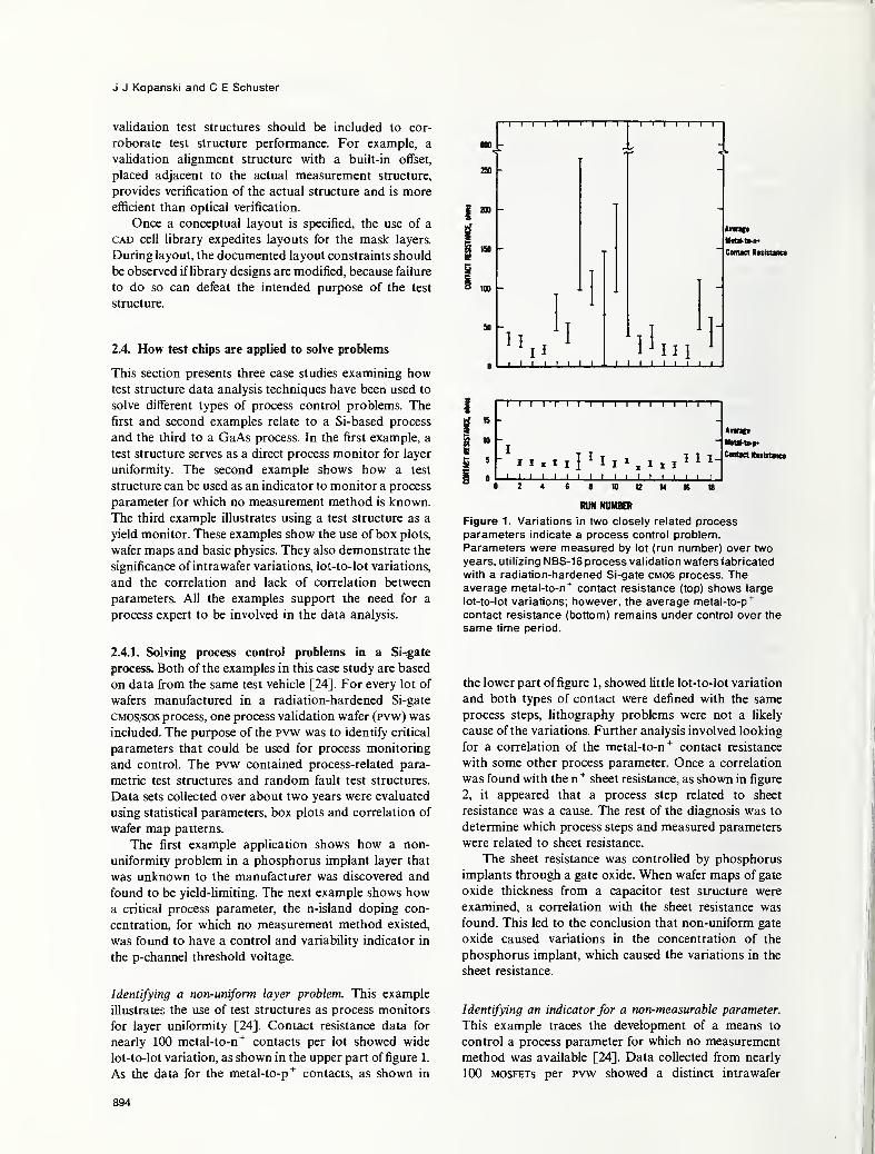
J J Kopanski and C E Schuster
validation test structures should be included to cor-
roborate test structure performance. For example, a
validation alignment structure with a built-in offset,
placed adjacent to the actual measurement structure,
provides verification of the actual structure and is moreefficient than optical verification.
Once a conceptual layout is specified, the use of a
CAD cell library expedites layouts for the mask layers.
During layout, the documented layout constraints should
be observed if library designs are modified, because failure
to do so can defeat the intended purpose of the test
structure.
2.4. How test chips are applied to solve problems
This section presents three case studies examining howtest structure data analysis techniques have been used to
solve different types of process control problems. The
first and second examples relate to a Si-based process
and the third to a GaAs process. In the first example, a
test structure serves as a direct process monitor for layer
uniformity. The second example shows how a test
structure can be used as an indicator to monitor a process
parameter for which no measurement method is known.
The third example illustrates using a test structure as a
yield monitor. These examples show the use of box plots,
wafer maps and basic physics. They also demonstrate the
significance of intrawafer variations, lot-to-lot variations,
and the correlation and lack of correlation between
parameters. All the examples support the need for a
process expert to be involved in the data analysis.
2.4.1. Solving process control problems in a Si-.gate
process. Both of the examples in this case study are based
on data from the same test vehicle [24]. For every lot of
wafers manufactured in a radiation-hardened Si-gate
CMOS/SOS process, one process validation wafer (pvw) was
included. The purpose of the pvw was to identify critical
parameters that could be used for process monitoring
and control. The pvw contained process-related para-
metric test structures and random fault test structures.
Data sets collected over about two years were evaluated
using statistical parameters, box plots and correlation of
wafer map patterns.
The first example application shows how a non-
uniformity problem in a phosphorus implant layer that
was unknown to the manufacturer was discovered and
found to be yield-hmiting. The next example shows howa critical process parameter, the n-island doping con-
centration, for which no measurement method existed,
was found to have a control and variability indicator in
the p-channel threshold voltage.
Identifying a non-uniform layer problem. This example
illustrates the use of test structures as process monitors
for layer uniformity [24]. Contact resistance data for
nearly 100 metal-to-n"^ contacts per lot showed wide
lot-to-lot variation, as shown in the upper part of figure 1.
As the data for the metal-to-p"^ contacts, as shown in
m
i™
5
a nn
so -
-I—i—i—I—t—1—r—
r
ll
I I I
"T—I—I—I—I—I—
r
Milr I I I I
t<mp
Coiitict RtststSK*
5-
I I I I I I I I I I I I I I I I I
I I I I I Ill I I I-
'II I I I I ' I I I I
Afmp
Cartaet toiitaict
RUN NUMBER
Figure 1. Variations in two closely related processparameters indicate a process control problem.
Parameters were measured by lot (run number) over twoyears, utilizing NBS-16 process validation wafers fabricated
with a radiation-hardened Si-gate cmos process. Theaverage metal-to-n* contact resistance (top) shows large
lot-to-lot variations; however, the average metal-to-p*
contact resistance (bottom) remains under control over the
same time period.
the lower part offigure 1, showed httle lot-to-lot variation
and both types of contact were defined with the same
process steps, lithography problems were not a likely
cause of the variations. Further analysis involved looking
for a correlation of the metal-to-n"^ contact resistance
with some other process parameter. Once a correlation
was found with the n sheet resistance, as shown in figure
2, it appeared that a process step related to sheet
resistance was a cause. The rest of the diagnosis was to
determine which process steps and measured parameters
were related to sheet resistance.
The sheet resistance was controlled by phosphorus
implants through a gate oxide. When wafer maps of gate
oxide thickness from a capacitor test structure were
examined, a correlation with the sheet resistance was
found. This led to the conclusion that non-uniform gate
oxide caused variations in the concentration of the
phosphorus implant, which caused the variations in the
sheet resistance.
Identifying an indicator for a non-measurable parameter.
This example traces the development of a means to
control a process parameter for which no measurement
method was available [24]. Data collected from nearly
100 MOSFETs per pvw showed a distinct intrawafer
894
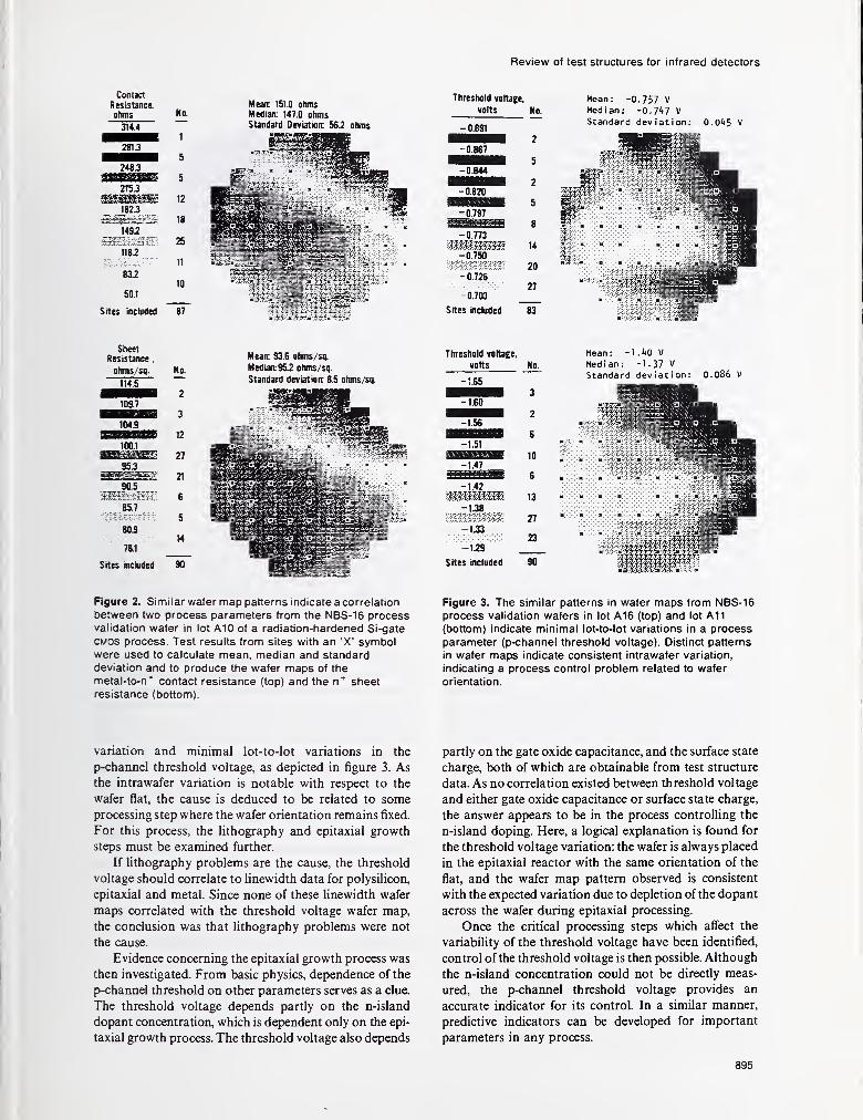
Review of test structures for infrared detectors
Contact
Resistance.
ohms
3144
281.3
215.3
_ J82J
149.2
632
50.1
Sites included
Ho.
1
5
5
12
18
25
11
10
Mean 151.0 ohmsMedian: 147.0 ohmsStandard Oeviatioti 56.2 ohms
Threshold voltage,
volts No.
-0.891
-0.867
-0.844
-0.820
-0.797
-0.773
iieMeii? 14
-0.750
20-0.726
27-0.703
Sites included 83
Mean: -0.757 V
Median: -0.7^7 V
Standard deviation:
Sheet
Resistance,
ohms/sn.
114.5
10a7
104.9
100.1
9Qi
'.''85.^'.
'tm''
Sites included
Ho.
2
3
12
27
21
6
5
M
lo"
Mean: 93.6 ohms/sq.
Median:95.2 ohnis/s(|.
Standard deviation: 8.5 ohms/sq.
Threshold valtace,
volts
-1.42
•'-lis''
Sites included
No.
3
2
6
10
6
13
27
23
90
Mean: -HO V
Median: -1 .37 V
Standard deviation: 0.086 V
Rgure 2. Similar wafer map patterns indicate a correlation
between two process parameters from the NBS-16 processvalidation wafer in lot A10 of a radiation-fiardened Si-gate
CMOS process. Test results from sites with an 'X' symbolwere used to calculate mean, median and standard
deviation and to produce the wafer maps of the
metal-to-n* contact resistance (top) and the n* sheetresistance (bottom).
Figure 3. The similar patterns in wafer maps from NBS-16process validation wafers in lot A16 (top) and lot A11
(bottom) indicate minimal lot-to-lot variations in a process
parameter (p-channel threshold voltage). Distinct patterns
in wafer maps indicate consistent intrawafer variation,
indicating a process control problem related to wafer
orientation.
variation and minimal lot-to-lot variations in the
p-channel threshold voltage, as depicted in figure 3. As
the intrawafer variation is notable with respect to the
wafer flat, the cause is deduced to be related to some
processing step where the wafer orientation remains fixed.
For this process, the lithography and epitaxial growth
steps must be examined further.
If lithography problems are the cause, the threshold
voltage should correlate to Unewidth data for polysilicon,
epitaxial and metal. Since none of these Unewidth wafer
maps correlated with the threshold voltage wafer map,
the conclusion was that lithography problems were not
the cause.
Evidence concerning the epitaxial growth process was
then investigated. From basic physics, dependence of the
p-channel threshold on other parameters serves as a clue.
The threshold voltage depends partly on the n-island
dopant concentration, which is dependent only on the epi-
taxial growth process. The threshold voltage also depends
partly on the gate oxide capacitance, and the surface state
charge, both of which are obtainable from test structure
data. As no correlation existed between threshold voltage
and either gate oxide capacitance or surface state charge,
the answer appears to be in the process controlling the
n-island doping. Here, a logical explanation is found for
the threshold voltage variation: the wafer is always placed
in the epitaxial reactor with the same orientation of the
flat, and the wafer map pattern observed is consistent
with the expected variation due to depletion of the dopant
across the wafer during epitaxial processing.
Once the critical processing steps which affect the
variabihty of the threshold voltage have been identified,
control of the threshold voltage is then possible. Although
the n-island concentration could not be directly meas-
ured, the p-channel threshold voltage provides an
accurate indicator for its control. In a similar manner,
predictive indicators can be developed for important
parameters in any process.
895
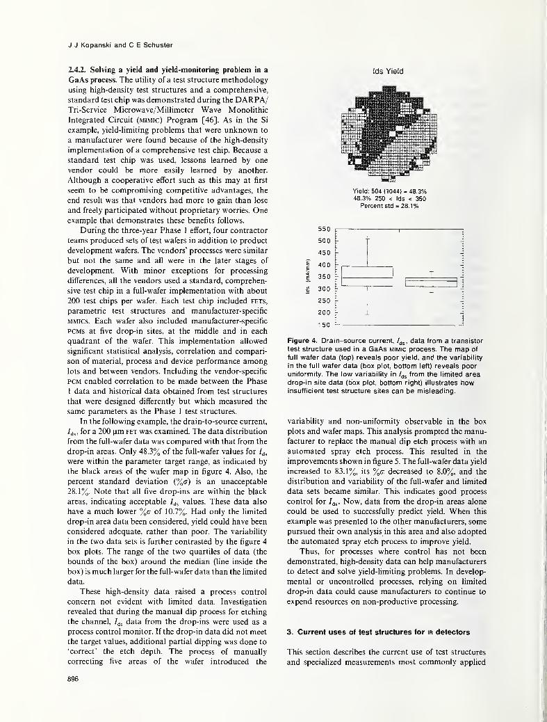
J J Kopanski and C E Schuster
2.4.2. Solving a yield and yield-monitoring problem in a
GaAs process. The utility of a test structure methodology
using high-density test structures and a comprehensive,
standard test chip was demonstrated during the DARPA/Tri-Service Microwave/Millimeter Wave Monolithic
Integrated Circuit (mimic) Program [46]. As in the Si
example, yield-hmiting problems that were unknown to
a manufacturer were found because of the high-density
implementation of a comprehensive test chip. Because a
standard test chip was used, lessons learned by one
vendor could be more easily learned by another.
Although a cooperative effort such as this may at first
seem to be compromising competitive advantages, the
end result was that vendors had more to gain than lose
and freely participated without proprietary worries. Oneexample that demonstrates these benefits follows.
During the three-year Phase 1 effort, four contractor
teams produced sets of test wafers in addition to product
development wafers. The vendors' processes were similar
but not the same and all were in the later stages of
development. With minor exceptions for processing
differences, all the vendors used a standard, comprehen-
sive test chip in a full-wafer implementation with about
200 test chips per wafer. Each test chip included fets,
parametric test structures and manufacturer-specific
MMics. Each wafer also included manufacturer-specific
PCMs at five drop-in sites, at the middle and in each
quadrant of the wafer. This implementation allowed
significant statistical analysis, correlation and compari-
son of material, process and device performance amonglots and between vendors. Including the vendor-specific
PCM enabled correlation to be made between the Phase
1 data and historical data obtained from test structures
that were designed differently but which measured the
same parameters as the Phase 1 test structures.
In the following example, the drain-to-source current,
for a 200 nm fet was examined. The data distribution
from the full-wafer data was compared with that from the
drop-in areas. Only 48.3% of the full-wafer values for I^^
were within the parameter target range, as indicated by
the black areas of the wafer map in figure 4. Also, the
percent standard deviation (%o-) is an unacceptable
28.1%. Note that all five drop-ins are within the black
areas, indicating acceptable I^^ values. These data also
have a much lower %(t of 10.7%. Had only the limited
drop-in area data been considered, yield could have been
considered adequate, rather than poor. The variability
in the two data sets is further contrasted by the figure 4
box plots. The range of the two quartiles of data (the
bounds of the box) around the median (line inside the
box) is much larger for the full-wafer data than the limited
data.
These high-density data raised a process control
concern not evident with limited data. Investigation
revealed that during the manual dip process for etching
the channel, I^^ data from the drop-ins were used as a
process control monitor. If the drop-in data did not meet
the target values, additional partial dipping was done to
'correct' the etch depth. The process of manually
correcting five areas of the wafer introduced the
Ids Yield
550 r-
500 i-
450 \r
250 ^ ^
200 E- i^
150 ^ 5
Figure 4. Drain-source current, /^^. data from a transistor
test structure used In a GaAs mimic process. The map of
full wafer data (top) reveals poor yield, and the variability
in the full wafer data (box plot, bottom left) reveals pooruniformity. The low variability in 1^^ from the limited area
drop-in site data (box plot, bottom right) illustrates howinsufficient test structure sites can be misleading.
variability and non-uniformity observable in the box
plots and wafer maps. This analysis prompted the manu-facturer to replace the manual dip etch process with an
automated spray etch process. This resulted in the
improvements shown in figure 5. The full-wafer data yield
increased to 83.1%, its %cr decreased to 8.0%, and the
distribution and variability of the full-wafer and limited
data sets became similar. This indicates good process
control for I^^. Now, data from the drop-in areas alone
could be used to successfully predict yield. When this
example was presented to the other manufacturers, some
pursued their own analysis in this area and also adopted
the automated spray etch process to improve yield.
Thus, for processes where control has not been
demonstrated, high-density data can help manufacturers
to detect and solve yield-hmiting problems. In develop-
mental or uncontrolled processes, relying on limited
drop-in data could cause manufacturers to continue to
expend resources on non-productive processing.
3. Current uses of test structures for ir detectors
This section describes the current use of test structures
and specialized measurements most commonly applied
896;;

Review of test structures for infrared detectors
Ids Yield
Yield: 893 (1074) = 83.1%83.1% 250 < Ids < 350
Percent std = 8.0%
550 -
500 f-
450 ^_ t
I400 r
1 350 j-
§ 300 [
250f-
200I
Figure 5. Following process modifications indicated from
test structure results, wafer maps of /^^ show improved
and controlled yield (top). Once the yield-limiting problemswere controlled, the variabilities of the data from the full
wafer (bottom left) and the limited area drop-in sites
(bottom right) became comparable.
to IR detector devices, processes and materials. Section
3.5 presents a comprehensive listing of devices that are
well described in the literature and that are thus
candidates for inclusion in m detector test chips.
IR detectors are fabricated as a wide range of devices
based on a variety of materials, with a number of basic
device structures, and encompassing everything from
discrete detectors to large infrared focal plane arrays
(iRFPAs). Most of the following discussion focuses on
photovoltaic (f>-n junction) diodes fabricated in HgCdTe,
the technology with currently the most pressing and
challenging applications for test structures. However,
other significant devices, such as photoconductive and
MIS detectors, and materials such as CdTe and silicon,
are included as appropriate.
3.1. Similarities and differences with Si and GaAs ics
iR detectors share some concepts in common with silicon
ICS and GaAs mmics: they are produced with much the
same equipment and processes, and they have similar
types of device structures. Some irfpas are nearing the
same complexity and dimensions as large-scale integra-
tion (LSI) Si memory chips. Like memories, detector
arrays contain many similar, regularly spaced devices.
However, there are pronounced differences between
IR detectors and ics. Infrared detectors are photosensitive
devices which interact with electromagnetic radiation,
similarly to Si photovoltaic solar cells. Many ir detectors
require a narrow-bandgap semiconductor, such as
HgCdTe, and must be operated at low temperatures. The
need to characterize the material and devices as a function
of incoming Hght and at low temperature has often
necessitated that test structures be packaged and cooled
in a Dewar before measurement.
Hgi_j.Cd^Te (HgCdTe) is a compound semicon-
ductor whose electrical and optical properties are a
function of composition. Detector performance is thus
dependent upon composition, and arrays of detectors
with uniform responses require material highly uniform
in composition. Many detector apphcations also require
thin layers of active material, requiring a precisely
controlled thinning process. HgCdTe materials are grown
by a variety of methods, including bulk growth,
liquid-phase epitaxy (lpe), metal-organic chemical
vapour deposition (mocvd) and molecular beam epitaxy
(mbe). The evolving crystal growth technology demands
test structures and characterization procedures to eval-
uate material quahty, uniformity and process effects
rapidly and precisely.
Compared with Si, HgCdTe is easily damaged by
temperature and radiation. Many fabrication processes
can change the properties of the material by distributing
composition or introducing electrically active defects.
Test structures can be used to monitor such changes, as
in the use of mis capacitors to quantify ion milling damage
[47]. Damage caused by contact with mechanical probes,
especially in the active region of a device, can change the
electrical properties of the material.
Compared with many semiconductor products, ir
detectors are currently produced in low volume and with
yields that are often very low. The starting substrates
have small surface areas and, for some applications, the
highest quality material is not plentiful. As a consequence,
manufacturers have been reluctant to devote large areas
on each substrate or in each fabrication lot, to test
structures. In fact, the completed ir detectors themselves
often serve as the primary test structures.
3.2. Characterization needs and concerns
ir detector material and producibility issues were
reviewed in the keynote addresses at the 1991 HgCdTeWorkshop [48, 49]. Here are a few of the key areas
that are of general concern for HgCdTe photovoltaic
materials, processes, devices and packages:
Materials. The uniformity of electrical and optical
properties that depend upon composition, defects and
dopant variations is a pressing concern for Hg, .^Cd^^Te.
To achieve a uniform device response over large areas,
a low density of bulk defects and rigorous control of
surface effects are required. With any photosensitive
device, the critical parameters which determine device
response are those which describe the recovery of the
897
J J Kopanski and C E Schuster
semiconductor to equilibrium: minority carrier lifetime
T, diffusion length L and surface recombination velocity
So.
Processes. Surface effects often dominate ir detector
performance. Characterization of the process by which
the passivation layer is formed and the quality of that
passivation layer are therefore critical. The choice of
passivation is more complex for HgCdTe than for Si, with
no obvious optimum process for all applications from
the wide variety of potentially useful native and deposited
insulating layers examined to date.
Increasingly with future generations of detectors,
performance will depend on the carefully tailored
variations in material properties with depth. A variety of
techniques is available to determine dopant profiles
with depth (such as secondary-ion mass spectrometry
(siMS), neutron depth profihng and junction capacitance-
voltage dopant-depth profiling), but existing non-
destructive techniques are limited in their abihty to
resolve variations between multiple nanoscale layers.
Devices. Characterization of the individual detector
performance and variations among detectors is of
obvious concern, and is often addressed with test
structures, i.e. detector elements fabricated especially for
this purpose.
Infrared detectors are produced in four major classes
of photon detectors (photoconductive, photovoltaic (p-n
junctions), metal-insulator-semiconductor (mis) and
Schottky barrier), each with different device characteriza-
tion concerns. Photoconductive detectors (see the review
by Broudy and Mazarczyck [50]) contain no rectifying
junctions, limiting the complexity of test structures. For
photovoltaic detectors (reviewed by Reine et al [51]), the
electrical characteristics of the p-n junction photodiodes
must be determined, typified by the product of the
photodiode dynamic resistance at zero-bias voltage and
junction area, RqA. Much effort has been devoted to
understanding the origins of and controlling the dark
current and noise. Metal-insulator-semiconductor photo-
capacitors (reviewed by Kinch [52]) are characterized
by their capacitance and conductance versus voltage
behaviour. An RqA value is also an important figure of
merit for mis detectors, as well as other mis properties
including: the interface charges, tunnelling currents and
the storage time of the mis device. Schottky diodes sue
characterized by the Schottky barrier height.
Package. Practical detectors depend on sophisticated
interconnect and packaging techniques for interfaces with
additional signal processing electronics, for interfaces
with the incident signal and for permanent installation in
Dewars. The rehability of the device, interconnect and
package is often characterized by elevated temperature
bake-out and thermal cycling.
33. Current approaches to test structure use
For IR detectors, a larger emphasis has been placed on
the quality of the detector performance, rather than the
direct measurement of specific material and process
parameters with test structures. Electrical characteristics
and figures of merit of detector elements, such as RqA,
have been used as diagnostic tools. Measurements of
material parameters have been developed using detector
array elements as the test structure, i.e. using the RqA of
a photovoltaic detector as a measure of the lifetime of
the material [53, 54], and estimating diffusion length by
injecting current at one diode and determining the change
in leakage at an adjacent diode.
Considerable pre-detector-fabrication characteriza-
tion also takes place. For example, it is common practice
to make use of a 'fast diode' process. This is a
minimum-step, fast turn-around, diode process which can
be fabricated on a comer of a substrate and be used to
evaluate the quality of the material from the qualities of
the 'fast diodes'. Prefabrication characterization also
commonly includes Hall effect measurements and manyof the non-test-structure characterization techniques
discussed in the next section.
As far as test structures are concerned, a commonstrategy has been to make use of a series of devices which
differ in one physical aspect and to see how that variation
affects the measured electrical properties. Devices of this
type include: (1) variable area diodes, (2) constant area,
variable perimeter diodes [55], (3) diodes with varying
contact metal areas [56] and (4) diodes with contact pads,
both on the diode and off the active area.
As mentioned above, measurements are often not
conducted until the devices have been packaged. Measure-
ments on bonded devices from an m detector process are
often more repeatable and reliable than measurements
using a probe station. The background photon flux can
be difficult to control and quantify in measurements with
probe stations. Also, determination of crosstalk and 1//
noise is much easier with packaged devices. However,
the increased time and cost of packaging devices has no
doubt hindered test structure apphcations in HgCdTe.Recent advances in probe station technology incorporate
both low temperature and the use of a non-contact probe
adapted from a scanning tunnelhng microscope [57], and
may facilitate greater pre-packaging test.
Despite the emphasis on other characterization
procedures, test structures and test chips more along the
hnes of those applied in the silicon ic industry have been
developed. Test chips consisting of both drop-ins for
inclusion with product wafers and complete wafers of test
chips for statistical parameter characterization are
available for use in the m detector industry. A layout of
a test chip with a comprehensive set of test structures,
courtesy of Rockwell International Inc.f, is shown in
figure 6. This test chip, for an epitaxial, photovoltaic
detector process, contains a mini-array of detectors,
variable area diodes, mis capacitors, hthographic Hall
t Certain commercial equipment, instruments or materials are
identified in this paper in order to adequately specify the
experimental procedure. Such identification does not imply
recommendation or endorsement by NIST, nor does it imply that
the materials or equipment used are necessarily the best available for
the purpose.
898
Review of test structures for infrared detectors
Rgure 6. The comprehensive test chip for an epitaxial
layer, HgCdTe photodiode process designed by McLevigeat Rockwell International Corp., Science Center. (Courtesy
Rockwell International Inc., with special thanks to M VMcLevige and J Bajaj.)
effect structures and transmission line test structures.
Uses of each of these classes of test structures are included
in the discussion that follows.
3.4. Non-test-stnicture characterization
Due in part to the deUcate nature of HgCdTe, various
optical and non-contact electrical methods have been
highly developed and applied to HgCdTe. In practice,
these non-contact techniques play at least as large a part
as test structures in the characterization of the material
and processes. A complete review of such techniques is
not possible here. However, any discussion of test
structures must take into account the functions of several
prevalent non-test-structure characterization techniques.
In particular, optical infrared transmission measure-
ments are universally available to determine wafer
composition (bandgap energy) and epitaxial layer thick-
ness [58]. Instruments are available that can rapidly
produce compositional maps of bandgap energy at nine
or more points evenly spaced across the HgCdTe surface.
Photoreflectance [59] provides a non-contact and
low-temperature method with which to determine
optical transition lineshapes and information on com-
position and defects. Other commonly applied optical
techniques include: visible and far-infrared reflectivity,
ellipsometry, electrolyte electroreflectance and laser-
beam-induced current (lbic) images of electrically active
defects [60]. Also prevalent are non-contact methods to
measure lifetime [61], such as optically modulated
absorption, microwave transmission or reflection techni-
ques, and the frequency response ofphotoluminescence.
Destructive characterization techniques are also used.
Dopant density as a function of depth has been
determined by ion sputtering in conjunction with siMS,
Auger and x-ray photoelectron spectroscopy [62]. Asimple measure of dislocation density and uniformity is
the etch pit density (epd) following exposure to an etchant
[63]. Electron-beam-induced current (ebic), usually
measured in a scanning electron microscope (sem), is used
to determine minority carrier difi"usion length [53, 64].
3.5. Specific test structures
Of the wide variety of test structures that have been
developed for Si and GaAs, a smaller subset has been
adapted for use with er detector technology. This section
contains a comprehensive listing of the test structures
and some of the test methods used to characterize ir
detector devices, processes and materials. Design con-
siderations and the uses of each test structure are
discussed. Most test structures were originally developed
on the basis of Si technology. References in this section are
made to applications to HgCdTe, along with a few key
references to the original applications in Si.
33.1. Detector array elements as test structures. Detector
array elements themselves, and mini-arrays (of around
five-by-five elements), are important test structures.
Separate elements for test allow the detector response to
be characterized without compromising a functional
array. Since the adjacent elements can limit the optical
area and otherwise alter the response of a detector
element, mini-arrays are useful to determine device
performance while surrounded by other functioning
detectors. For ease of interpretation, it is desirable for
characterization to be made on detectors identical to
working array elements. Variable-area diodes, discussed
in the next section, can also be used for this sort of
measurement and offer the advantage of quantifying the
perimeter and area dependence of any measurement.
Array elements have been used to characterize the
detectors themselves, the noise and crosstalk, and to
estimate minority carrier lifetime.
Detector characterization. Detector elements are quanti-
fied and compared by means of several well known figures
of merit, which are discussed in detail in previous reviews
[51, 52, 65]. The response of an infrared detector to an
incident signal is characterized by the responsivity, jR, in
VW~\ the quantum efficiency, tj, the relative spectral
response at the cut-off and peak wavelength, and /i^^^y.,
in )im, and the time constant of the frequency response,
T in s. The signal-to-noise ratio of the elements is
characterized by the noise equivalent power, nep, in WHz"^'-^, and the normalized detectivity, D*, in cm Hz''^
W~ ^ Capacitance-voltage dopant-depth profihng of the
p-n junction photodiode has also been commonly
implemented [64, 66].
Noise characterization. The sources of current noise in
photodiodes include: Johnson-Nyquist noise of the
899
J J Kopanski and C E Schuster
zero-bias impedance, IkT/R^^, shot noise, thermal noise
due to thermally generated dark currents, and 1// noise,
which is characterized by a spectrum that varies as 1//",
with a close to 1 [51, 67].
Much effort has been devoted to the characterization
and reduction of excess 1// noise, a limiting factor in the
performance of photodetectors and focal plane arrays
[68-71]. Understanding the origins of 1// noise is critical
to guide actions to reduce it. Measurement of the noise
versus frequency spectrum is straightforward (see, for
example, the experimental set-up in [70]). Noise current
density is usually measured over frequencies in the range
of 1 Hz to 10 kHz, and also as a function of diode reverse
bias and temperature. The 1// noise has been correlated
with detector bias, temperature, diode area and surface
leakage currents [69, 71]. More detailed noise studies
require a set of variable-area diodes, as discussed below,
so that the surface or bulk origin of the noise, the
mechanism that generates noise, and the relationship
between noise and dark current can be determined [17].
Crosstalk determination. The influence of adjacent ele-
ments potentially affects the spatial and frequency
resolution of detector array elements. The most straight-
forward method to quantify crosstalk is to measure the
response of an element which is blocked to irradiation
while operating adjacent (non-blocked) elements. Alter-
natively, a focused monochrome beam can be used to
actuate individual elements while monitoring the res-
ponse of adjacent elements.
Minority carrier lifetimefrom zero bias resistance product.
For n"^ on p junction photodiodes, an estimate of
minority carrier lifetime can be obtained from the
measured RqA versus temperature, T, via [53, 54]
RoA = {NJqnf\kTlqy^\zJnyi^ (1)
where TV^ is the base acceptor concentration, q is the
electron charge, k is Boltzmann's constant, is the
minority electron lifetime and is the electron mobility.
The intrinsic carrier concentration, n„ is calculated from
expressions relating it to x, T and the bandgap, £g [54,
72]; mobility is obtained from published data, and
estimates of from Hall measurements before device
fabrication.
3^.2. Variable-area diodes. The perimeter-to-area ratio,
P/y4j, of a square or circular diode will increase as the
length of its side or radius is made smaller. Thus, a
smaller-area diode will be more dependent on perimeter
or surface effects and less dependent on area or bulk
effects than a diode with the same shape but a larger
area. This natural separation of surface and bulk effects
makes a series of diodes with varying areas a powerful
test structure for the evaluation of the potential
performance of infrared photovoltaic devices, as well
as the quality of the material, process and surface
passivation.
Variable-area diodes refer to a series of three or more
p-n junction diodes, identical except for their area.
Usually, the diodes are square or circular with junction
areas varying by about three orders of magnitude, for
example a set of five diodes with areas from 9.0 x 10"^
to 2.5 X 10"^ cm^ [70]. Some variable-area-diode test
structures have been designed with contacts off the active
area (to eliminate damage induced by wire bonding) [70]
and with a biasable guard ring (to better define the
effective optical area of the diode) [73]. Variable-area
diodes have been used to evaluate differences in diodes
formed in the mesa or planar structures, as well as the
qualities of different passivation procedures. A variation
of this test structure would be a series of diodes with
constant area, but variable perimeter (i.e. with different
shapes) [55].
Parameters measured with variable-area-diode test
structures include RqA, dark current density and/or noise
current density, often as a function of temperature.
Cahbration of the actual fabricated diode areas versus
designed diode areas would also be desirable. Variable-
area diodes have been used to determine the P/Aj
dependence of {R^AY^, the area dependence of the noise
current, and the l/T dependence of RqA.
{RqA)~^ versus P/Aj. RqA^ has been modelled as a sum
of bulk-dependent and P/Aj proportional terms [74]:
{RoA)-' = (/?o^)b"Jk + (<7"iSo lV,/V^.)(P/Ai) (2)
where Sq is the surface recombination velocity in the
depletion region where it intersects the HgCdTe surface,
Wq is the depletion width at zero bias and F^j the built-in
potential of the junction. The slope of the plot of (/?o^)~
'
versus P/A^ is proportional to Sq, while the projected
intercept with P/A^ = 0 (corresponding to an infinite
diode) gives (i?o^)buik- (^o^)buik is characteristic of the
film and should not be dependent on diode geometry or
process variations [75]. The degree that {RqA)~^ depends
on P/Aj is a relative measure of the influence of surface
originating currents on device behaviour. The ideal case
is for the lowest possible contribution from surface
currents, a low surface recombination velocity (Sq
approaching 0), and no P/Aj dependence.
A linear trend is only observed when hole diffusion
lengths, Z-h, are short compared with diode radii [75].
When Ly, is long compared with diode radii, a significant
component of the dark current will be due to lateral
diffusion. In this case, smaller diodes will have a larger
proportion of diffusion current than larger diodes, and
(^0^)"' versus P/A^ will have a parabohc dependence
[75, 76].
If dark current is proportional to (RqA)'^, it would
be expected to show the same type of P/A^ dependence.
Noise current density versus Ay In an analogous manner,
variable-area diodes have been used to determine whether
noise currents in midwavelength infrared (mwir) diodes
originate at the surface or in the bulk [70, 77]. The
analysis is based on Hooge's empirical equation for the
noise power spectral density, Sj, in p-n junctions [70, 78]:
S, = a^PlfN. (3)
900
Review of test structures for infrared detectors
Here, aH is a fitted parameter referred to as the Hoogeparameter, / is the current flowing in the system and A'^
the number of carriers. Noise current is the square root
of S,. If the noise is due to an area (bulk) source, then
both / and N should var\' as the diode area, and noise
current density should depend on A^'^. If the noise is due
to a perimeter (surface) source, then both / and A'^ should
vary as the square root of diode area, and noise current
density should depend on /l^'*.
RqA and/or dark current density versus 1/T. The
temperature dependence oi RqA and dark current density
can be used to separate the contribution of diffusion
currents and generation-recombination (g-r) currents
to the total current [56. 70, 79]. Insight into the origin
of the dominant current components in infrared detectors
has been useful in optimizing device performance.
Common practice is to measure Rq in a temperature
range where the dominant carrier mechanism is changing.
A plot of Rq versus I T is then compared with hnes
approximating diffusion current (l/nf temperature-
dependence dommated)
i?o/lD.FF = {kT/q^)iNJnf)(rJD„y" (4)
and generation-recombination current (l/nj temperature-
dependence dominated) [79, 80],
RoAc-K = [(Na/cJA) ln(N^No/nf)V'^izJqn,) (5)
where the subscripts diff and g-r refer to the contribu-
tions of diffusion and generation-recombination cur-
rents. resp>ectively.
From the known behaviour of current-generating
processes, diffusion currents are expected to dominate at
temperatures higher than around 50 K, while g-r current
dominance is expected at lower temperatures. Deviations
from the g-r line at lower temperatures are often assumed
to be from unknown sources of (most likely) surface
leakage [56, 79]. However, tunnelling is often the
dominant current mechanism in HgCdTe. Measurements
on diodes consisting of n^ on bulk p-type Hg^.^Cdj-Te
(x =r 0.22) have shown that Rq is diffusion-current
dominated at high temperatures, while at lower tempera-
tures, trap-assisted and band-to-band tunnelling currents
dominate depending on reverse bias and temperature [56,
66].
An activation energy can be extracted from the inverse
temperature dependence of dark current density and
noise current densities using an Arrhenius-type equation
[70]. The activation energy of the dark current should
relate to the energy bandgap, while the activation energy
of the 1// noise current has been related to the location
of g-r centres at about 0.75£g within the bandgap.
Mini or lithographic Hall effect test structures. Hall
effect measurements are of central importance to the
characterization of detector materials as they provide
reliable values for carrier concentration and mobility.
Hall measurements can be made on small, lithographic-
ally fabricated structures, as well as on the bulk samples.
Most interpretation has been developed under the
assumption of sample homogeneity perpendicular to the
magnetic field. Lithographic Hall bars provide data from
a more localized area. When fabricated as part of a
detector process, lithographic Hall bars can be made from
both the substrate and any epitaxial layer(s). A variety
of lithographic Hall bar and van der Pauw geometries
have been used [81, 82]. For a discussion of design
considerations for lithographic Hall test structures, see
[11, 83].
To make the measurement most useful, the key
concern is interpretation of the Hall effect measurements
and relating the measured electrical quantities to the
semiconductor electrical properties. This is particularly
important for the case of two-layer structures [84], such
as epitaxial layers, which are common in detector
technology.
More detailed magnetotransport measurements, as a
function of magnetic field and temperature, are of great
interest for infrared detector materials because of the
coexistence of multiple-carrier species [85]. For example,
for p-type HgCdTe, variable magnetic field Hall effect
measurements have yielded the Hg vacancy ionization
energies, as well as carrier concentrations and mobilities
for the majority carriers (heavy holes), minority carriers
(electrons) and light holes [86].
The lithographic Hall effect structure can also be used
in a variety of other measurements. Conductivity/
resistivity measurements are commonly made in conjunc-
tion with Hall effect. With the addition of a source of
illumination, Hall effect can be extended to the photo-
Hall effect [87, 88] or the light-modulated Hall eff'ect
[89], which provides a measure of electron mobihty in
p-type material. Hall effect structures are also used for
the photoelectromagnetic (pem) effect (which can provide
a measure of surface recombination velocity) [90-92],
Shubnikov-de Haas effect (oscillatory magnetoresist-
ance) [93], and photoconductivity (lifetime) measure-
ments.
The Hall effect measurement has been used as a
monitor of processing effects on materials, for example,
ion beam milling effects on the surface of HgCdTe [47].
3.5.4. Methods to determine lifetime. Carrier hfetime is
an essential physical parameter for a complete description
of the response of any ir detector material. A variety of
contact methods, or methods using simple test structures,
have been employed in the measurement of carrier
lifetime in m detector materials.
For a recent review of the issues and techniques for
the measurement of lifetimes in HgCdTe, see the paper
by Lopes et al in this issue [61]. An important issue in
the measurement of lifetime is the distinction between
lifetime measured by transient methods versus steady-
state methods [94]. Significant differences between
transient and steady-state lifetime have been detected and
are a function of minority carrier trapping [94]. The
steady-state hfetime appears to be more significant for
device performance and a more appropriate measure of
material quahty [94].
901
J J Kopanski and C E Schuster
Lifetime measurements are often conducted as a
function of temperature, carrier concentration and
composition. The dependence of the lifetime on these
variables has been used to identify the dominant
generation-recombination process within the test struc-
ture [64]. Minority carrier lifetime has been related to
bandgap and carrier concentration [61]. The difference
in lifetime between impurity-doped and vacancy-doped
HgCdTe has been studied [94]. The temperature
dependence of lifetime has been used to determine the
trap energy and density of bulk Shockley-Read centres
[64, 95]. The most common methods of determining
carrier hfetimes in HgCdTe include the following.
Photoconductive decay (pcd). In the photoconductive
decay technique, lifetime is determined from the slope or
1/e point of the current or voltage decay following
irradiation with a short laser pulse. The theory and
measurement instrumentation is described in some detail
in [81, 82, 95-97]. The pair of (ohmic) contacts required
for measurement of lifetime by pcd has been obtained
from simple circular dots. Hall devices [94], a multiprobe
Hall bar with six sets of contacts spaced 5 x 10~-^cm
apart down the length of the sample [81], and using a
pair of plated electrodes, each covering about one-third
of the wafer perimeter, allowing mapping of lifetime over
a circular wafer [95]. The measurement can also be madeon an mis capacitor and ohmic contact, providing a
measure of surface recombination velocity [98]. The
measurement is dependent on the spacing and size of the
contacts, which must be chosen to avoid minority carrier
sweep-out [99]. Lifetimes measured by pcd and by
optically modulated absorption have been compared
[96], as well as lifetimes by the pcd, photoconductivity
and PEM techniques [91].
Diode reverse-bias pulsed recovery technique (prt). Thepulsed recovery technique determines lifetime by the
recovery of the current following an abrupt reversal of a
junction from forward to reverse bias. The theory and
instrumentation for HgCdTe photodiodes is summarized
in Polla et al [64]. A simple interpretation of prt
measurements, developed for Si diodes without neces-
sarily abrupt junctions [100], is applicable to HgCdTe[64]. Both p-n junction [64] and Schottky barrier [101]
diodes have been used in the measurement.
Steady-state photoconductivity. For the steady-state
photoconductivity measurement, the sample is illumi-
nated with a laser or blackbody through a low-frequency
chopper and the PC signal measured by a lock-in [47, 91,
94]. The measured photoconductive signal is proportional
to fi„t„. The technique is dependent on a separate
measurement of minority carrier mobihty. The light-
modulated Hall effect has been used for this mobility
measurement [90]. The steady-state photoconductivity
measurement was then made with the same Hall devices.
Zero-bias resistance-area product. The determination of
lifetime from the RqA product of a p-n junction
photodiode [53, 54, 79] is described in section 3.5.1.
Photoconductivefrequency response {frequency domain or
frequency roll-off). The lifetime of a semiconductor can
be obtained from the short-circuit ac photocurrent as a
function of light intensity modulation frequency response
of a diode [102, 103]. Photocurrent (or responsivity of
a photodiode) is plotted versus chopping frequency. Thehfetime and fall-off frequency are related. The test
structure is a photodiode or Schottky contact.
Photoelectromagnetic effect (pem). A discussion of the
technique and considerations for its application to
HgCdTe is given in [90]. In the photoelectromagnetic
effect, a magnetic field is applied perpendicular to a
diffusion current of optically generated excess carriers.
Analysis of the pem current, /pem. versus magnetic field
gives surface recombination velocity, carrier mobility and
bulk lifetime. The test structure used is the Hall bar. Bycombining photoconductivity and pem measurements,
both bulk minority carrier Hfetime and mobility can be
obtained [91].
3.5.5. Metal-insuiator-semiconductor (mis) capacitors.
Metal-insulator-semiconductor capacitors can be fabri-
cated along with photovoltaic detectors, as well as mis
photocapacitor detectors. The capacitors can be formed
on all layers of an epitaxial process. Information about
the semiconductor, the insulator, and the semiconductor-
insulator interface can be obtained. The mis test structure
should incorporate a guard-ring gate, surrounding the
primary mis capacitor, to isolate the test structure from
the surrounding surface [104].
The various insulators and passivation schemes used
in infrared detectors have recently been reviewed [105].
Insulating layers for mis capacitors on HgCdTe consist
of either deposited dielectric films or thin native films
with an overcoat of a deposited dielectric. Popular
passivation materials for HgCdTe include: evaporated or
sputter-deposited ZnS [90, 106-109], anodic (native)
oxide (usually with an overcoating of ZnS) [104, 110,
111], anodic (native) sulphide (usually with an overcoat-
ing of ZnS) [90-92, 1 12-114], SiOj (deposited by several
techniques) [115-117], evaporated Znj.Pbi_j.S [118],
SiN^ [105], anodic (native) fluoride [119] and other
II-VI compounds such as CdTe [120]. The mis capacitor
is the essential test structure for the evaluation and
comparison of passivation and insulating layers of
HgCdTe.Like photovoltaic diodes, mis photocapacitors have
been their own most important test structure. Keyparameters are the RqA product and the storage time,
Tj,. Storage time refers to the time required for minority
carrier dark current to fill the potential well resulting
from a voltage pulse of the mis capacitor into deep
depletion [52]:
Ts, = Q.K/J, (6)
where C„„ is the insulator capacitance, Kthe voltage pulse,
C„jF is the well capacity and is the total minority
carrier dark current density.
902
Review of test structures for infrared detectors
Beyond detector characterization, the mis capacitor
can be used for the determination and study of other
material, interface and process parameters:
Capacitance, conductance, and current versus gate voltage.
A large variety of standardized measurements developed
for Si Mos capacitors, as detailed in [121], has been
applied to mis capacitors on HgCdTe. Primarily, these
involve the measurement of the capacitance, conductance
and DC current of the mis capacitor as a function of gate
bias, AC measurement frequency, temperature, time and
illumination. Properties of the insulator that can be
obtained include thickness, resistivity, breakdown electric
field, insulator fixed charge and traps within the insulator.
The doping level of the bulk semiconductor is obtainable
from the change in capacitance from accumulation to
inversion, but more importantly, the formation and
dynamics of an inversion layer induced by the applied
electric field can be studied [112]. This can provide
insight into the minority carrier generation and recom-
bination rates and mechanisms. At the interface, the
properties of the fast and slow surface states can
be obtained, as well as an indication of the metal-
semiconductor work function [122] and the semi-
conductor-insulator barrier height. Interface states in
HgCdTe .MIS capacitors have often been quantified via
the conductance method [1 12, 116, 123], or the high/low
C-K technique [117].
The C-V of MIS capacitors has also been used to
profile the carrier concentration of ion-implanted junc-
tions in HgCdTe by fabricating an array of mis capacitors,
separated by 500 ^m, on a wafer whose surface has been
slant etched, resulting in a gentle grade in depth [91].
The properties of mis structures fabricated on double-
layer heterostructures, consisting of a 1 iim layer of
wide-bandgap HgCdTe on top of a 5 ^m layer of
narrow-bandgap HgCdTe, have also been reported
[124].
Unique concerns of mis capacitors from HgCdTe. Inter-
pretation of electrical measurements of HgCdTe mis
structures is not as straightforward as for an Si mos
[104, 112, 125, 126]. To adequately explain the observed
behaviour of mis capacitors on narrow-bandgap semi-
conductors, the following factors have to be considered:
(i) the non-parabolic conduction band [104, 126];
(ii) degeneracy in the occupancy of the free carriers
[104, 126];
(iii) comp)ensation and partial ionization of impuri-
ties and defects [126];
(iv) inversion layer quantization [104]; and
(v) interband or Zener tunnelling [104, 125].
As a consequence of conduction band degeneracy, the
most obvious effect on the measured C-K characteristics
is that the capacitance does not saturate in accumulation
for n-type capacitors, or in the strong inversion for p-type
capacitors in the low-frequency regime [104, 126].
Oscillations in G-K response of mis capacitors on p-type
HgCdTe are explained as arising from indirect (trap-
assisted) tunnelling and inversion layer quantization
effects [104, 127]. With the application of a magnetic
field, the formation of Landau levels in the two-
dimensional gas at the oxide/HgCdTe mis interface has
been observed at temperatures around 10 K [128]. Theoscillations in the C- V and G- V response are shifted by
an apphed magnetic field in a manner consistent with
tunnelling into the lowest Landau level associated with
each electric subband [128]. Spicer has pointed out that
due to the 'weak' Hg-Te bond, the bulk and surface
properties of HgCdTe intercommunicate and are moreclosely related in HgCdTe than in III-Vs and Si [129].
Defect and damage characterization. An important sub-
class of measurements concerns the determination of the
effects of radiation damage on the mis capacitor. Even
low levels of short-wavelength visible light can create
lateral non-uniformities in the fixed charge density of the
HgCdTe-insulator interface [104]. Visual light exposure
can result in a multiple flatband effect, though the effect
can be removed by annealing. The mis capacitor has also
been used as a monitor of ion-milling damage [47, 130].
Dislocations and hillocks have been observed to affect
the storage time and tunnelling currents of mis capacitors
on MBE-grown HgCdTe [110, 111].
3^.6. Gated p-n junction diodes and misfets. Gated
diodes and metal-insulator-semiconductor field-effect
transistors (misfets) are the most complex test structures
in common usage. They require formation of p-n junc-
tions, high-quality insulating layers and ohmic contacts.
Gated p-n junction diode. A gated p-n junction diode (gd)
consists of a p-n junction with a concentric mis gate
surrounding and slightly overlapping the junction at the
surface. A second, outer concentric gate is often employed
to isolate the gd from the surface beyond the inner gate
[115]. A gated diode is also formed by the gate and one
source/drain region of a misfet [131], though it is
preferred that the gate completely surround the junction.
The gate(s) of the gd offer the abihty to precisely control
the surface potential around the p-n junction. As a test
structure applied to ir detectors, gated diodes have been
used to localize and identify surface leakage effects and
currents, as well as to provide an indication of surface
recombination velocity and lifetime.
Typical characterization measurements include the
reverse junction current (at a series of fixed diode reverse
bias) and the RqA product as a function of gate voltage.
The outer guard gate (if it exists) would be held at a
constant voltage, usually to accumulate the surface as
determined from C- F measurements. The R^A product
is also measured as a function of gate voltage and l/T.
The gd has also been employed for C-F dopant profiling
of the region beneath the junction [66].
The well established interpretation of gated-diode
reverse current versus gate voltage characteristics for Si
gds is described in [132]. As with the mis capacitor, gds
in HgCdTe differ from those in Si; extensions of the
903
J J Kopanski and C E Schuster
existing theory to cover gds in HgCdTe are discussed in
[51, 113, 115]. In narrow-bandgap material (x ss 0.22)
and temperatures of 77 K and below, gated diode
behaviour is dominated by tunnelhng currents [51, 66,
113, 1 14, 133]. The surface potential determines whether
surface or bulk tunnelling prevails [113]. When the gate
is biased to cause accumulation of the surface adjacent
to the junction, surface tunnelling across the surface
junction dominates. When the area adjacent to the
junction has been inverted, tunnelling currents in the
field-induced junction dominate.
For HgCdTe with a wider bandgap (x x 0.45 to 0.3)
and at higher temperatures (145 K), gated diode charac-
teristics are closer to those of Si gds [115]. When the
gate is biased to cause accumulation of the surface
adjacent to the junction, the gated diode current is
dominated by trap and band-to-band tunnelling. Whenthe area adjacent to the junction is biased in depletion,
generation current from interface states will contribute
to the reverse-bias junction current. A measure of sur-
face recombination velocity, Sq, at the intersection of
the depletion region and the gate, can be obtained from
the magnitude of the current in this region [115, 133]. The
calculation is complicated due to uncertainties in the
effective area of the induced junction [133]. Whenthe area adjacent to the junction has been inverted,
the effects of surface generation are suppressed and the
effective area of the junction is increased by the
field-induced junction. The magnitude of the current in
this region is dependent on the minority carrier lifetime
in the metallurgical and field-induced junction.
Gated diode studies ofsurface passivation. The gated diode,
like the mis capacitor, is a useful test structure with which
to study surface effects. Measurements of noise and dark
currents in gated diodes as a function of temperature,
junction area and gate bias have been used to separate
bulk and surface mechanisms contributing to l/f noise
[113, 134]. Gated diode characteristics have been used
as a monitor of fixed charge and interface trapped charge
density in long-wavelength infrared (lwir) HgCdTe as
a function of gamma radiation total dose [133].
MiSFETs. Enhancement- and depletion-mode misfets in
HgCdTe [107, 114, 131, 135-137] and a metal-semi-
conductor FET (mesfet) in CdTe [135], as well as simple
digital circuits [106, 136, 138] have been reported, misfets
in Hgi_^Cdj.Te offer some prospect for monolithic
integration of signal processing functions with detectors
[131]. The suitability of fets for use in electronics circuits
is commonly assessed from their DC characteristics
(drain-to-source current as a function of drain-to-source
voltage and gate voltage, threshold voltage, surface
mobihty, etc) and small-signal ac characteristics (drain-
source resistance, amplification factor, transconductance,
etc) [106, 136]. Simple misfet digital invertor circuits on
HgCdTe have been characterized at speeds to 1 MHz[106].
misfets in HgCdTe have been used as test structures
to study quantum phenomena in reduced dimensions.
Subband spectroscopy, the observation of subbands due
to inversion layer quantization effects, has been reported
using gated diodes and misfets [107, 108]. misfets have
been used as a test structure for the quantum Hall effect
[139] and magnetotransport measurements [107]. By
changing the gate voltage on an HgCdTe misfet, the
magnetotransport of the two-dimensional electron gas
has been modulated from classical free electron behaviour
to weak-localization behaviour [107].
3.5.7. Ohmic and Schottky contacts. Simple metal-to-
semiconductor contacts are critical components of
detectors, and their behaviour must be characterized.
Ohmic and Schottky contacts are also employed as test
structures in a number of different types of measurement.
Theoretical models and experimental experience indicate
that for X < 0.4, metal contacts are expected to be ohmic
contacts on n-type and Schottky barriers on p-type
Hgi_^Cd^Te [140]. For x > 0.4, metal contacts are
expected to be Schottky barriers on both n- and p-type
material [140, 141].
Ohmic contacts. All detector structures require ohmic
contacts. High-quality ohmic contacts are essential for
photoconductive detectors. Ohmic contacts are charac-
terized primarily by their resistance, which can be divided
into components due to the semiconductor and to the
contact resistance. Methods to determine the specific
contact resistivity, the geometry-independent parameter
which describes the ohmic metal-to-semiconductor con-
tact, are described in the following sections.
Stable ohmic contacts have been used as test
structures to measure minority carrier hfetime via the
photoconductive decay technique, as well as for spreading
resistance [62], resistivity and contact resistivity. Resis-
tivity can be related to doping concentration and, at
room temperature, to the x value of Hgi_jCdjjTe [72,
142].
The defect structure and surface chemistry play an
important part in determining the quality of an ohmic
contact to HgCdTe [143, 144]. Ohmic contact test
structures have been used to evaluate the effects of the
contact formation process, surface preparation, inten-
tional interfacial layer formation and annealing [144].
Schottky contacts. Schottky barriers to HgCdTe are
themselves another class of photodiodes [101] and a
critical component necessary before a mesfet can be fab-
ricated [141]. Schottky contacts are commonly charac-
terized by their current-voltage and capacitance-voltage
responses. From the /-K characteristic, the diode ideality
factor, n, reverse leakage current and breakdown electric
field can be determined. The Schottky metal-to-semi-
conductor contact is characterized by the barrier height,
(/)b, which can be determined from I-V or C-Vmeasurements. The barrier height has also been obtained
from the activation energy of the variation of the
saturation current with inverse temperature [101].
Dopant density profiles have also been obtained from
C- K measurements [145].
904:
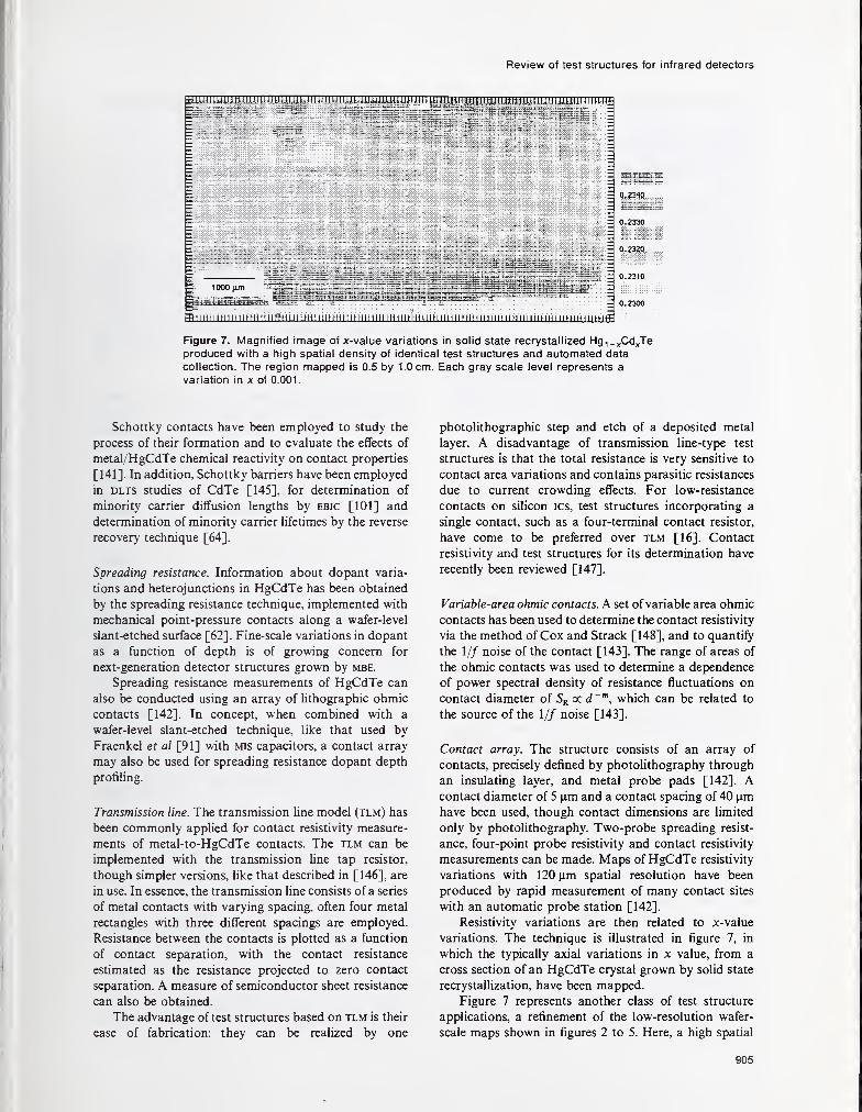
Review of test structures for infrared detectors
1000 iim 't^gj.L^
BflHIIIHIin iHri<lllflrllllMlinillllllllhllHIIIIIMIIIHIMMHIinii HliniHIMliirH1liihM
3 oaw.
0.2330
0.2320
Rgure 7. Magnified image of x-value variations in solid state recrystallized Hg,_j,Cd^Te
produced with a high spatial density of identical test structures and automated data
collection. The region mapped is 0.5 by 1.0 cm. Each gray scale level represents a
variation in x of 0.001.
Schottky contacts have been employed to study the
process of their formation and to evaluate the effects of
metal/HgCdTe chemical reactivity on contact properties
[141]. In addition, Schottky barriers have been employed
in DLTS studies of CdTe [145], for determination of
minority carrier diffusion lengths by ebic [101] and
determination of minority carrier lifetimes by the reverse
recovery technique [64].
Spreading resistance. Information about dopant varia-
tions and heterojunctions in HgCdTe has been obtained
by the spreading resistance technique, implemented with
mechanical point-pressure contacts along a wafer-level
slant-etched surface [62]. Fine-scale variations in dopant
as a function of depth is of growing concern for
next-generation detector structures grown by mbe.
Spreading resistance measurements of HgCdTe can
also be conducted using an array of lithographic ohmic
contacts [142]. In concept, when combined with a
wafer-level slant-etched technique, like that used by
Fraenkel et al [91] with mis capacitors, a contact array
may also be used for spreading resistance dopant depth
profiling.
Transmission line. The transmission line model (tlm) has
been commonly applied for contact resistivity measure-
ments of metal-to-HgCdTe contacts. The tlm can be
implemented with the transmission line tap resistor,
though simpler versions, like that described in [146], are
in use. In essence, the transmission line consists of a series
of metal contacts with varying spacing, often four metal
rectangles with three different spacings are employed.
Resistance between the contacts is plotted as a function
of contact separation, with the contact resistance
estimated as the resistance projected to zero contact
separation. A measure of semiconductor sheet resistance
can also be obtained.
The advantage of test structures based on tlm is their
ease of fabrication: they can be realized by one
photolithographic step and etch of a deposited metal
layer. A disadvantage of transmission line-type test
structures is that the total resistance is very sensitive to
contact area variations and contains parasitic resistances
due to current crowding effects. For low-resistance
contacts on silicon ics, test structures incorporating a
single contact, such as a four-terminal contact resistor,
have come to be preferred over tlm [16]. Contact
resistivity and test structures for its determination have
recently been reviewed [147].
Variable-area ohmic contacts. A set of variable area ohmic
contacts has been used to determine the contact resistivity
via the method of Cox and Strack [148], and to quantify
the 1// noise of the contact [143]. The range of areas of
the ohmic contacts was used to determine a dependence
of power spectral density of resistance fluctuations on
contact diameter of Sf^a:d~'", which can be related to
the source of the 1// noise [143].
Contact array. The structure consists of an array of
contacts, precisely defined by photolithography through
an insulating layer, and metal probe pads [142]. Acontact diameter of 5 |i.m and a contact spacing of 40 |im
have been used, though contact dimensions are limited
only by photolithography. Two-probe spreading resist-
ance, four-point probe resistivity and contact resistivity
measurements can be made. Maps of HgCdTe resistivity
variations with 120 |im spatial resolution have been
produced by rapid measurement of many contact sites
with an automatic probe station [142].
Resistivity variations are then related to x-value
variations. The technique is illustrated in figure 7, in
which the typically axial variations in x value, from a
cross section of an HgCdTe crystal grown by solid state
recrystallization, have been mapped.
Figure 7 represents another class of test structure
applications, a refinement of the low-resolution wafer-
scale maps shown in figures 2 to 5. Here, a high spatial
905

J J Kopanski and C E Schuster
density of identical test structures and automated data
collection are used to map variations in material
parameters (resistivity and x value). The technique results
in magnified images, such as would be obtained from a
microscope sensitive to resistivity and x-value variations.
3.5.8. Miscellaneous test structures.
Variably spaced diodes. Variably spaced diodes are used
to determine the minimum spacing at which adjacent
diodes short, thus providing an estimate of junction
spread. The same devices can be used to estimate diffusion
length by injecting current at one diode and determining
the change in leakage at an adjacent diode.
Deep-level characterization techniques. A variety of techni-
ques, which make use of the depletion region of a p-n
junction, Schottky barrier or mis capacitor, has been
employed to characterize deep levels in HgCdTe. These
include deep-level transient spectroscopy (dlts) [145,
149, 150], admittance spectroscopy (as) [150] and
thermally stimulated current (tsc) [150].
4. An expanded role for test structures?
This section contains suggestions for test structures with
potential applications to IR detectors. Section 4.2 contains
a discussion of how the silicon methodology can be
applied to HgCdTe ir detectors, as well as some practices
that the experience with silicon and GaAs test structures
suggests would be beneficial if applied to ir detectors.
4.1. Test structures with potential applications to mdetectors
The devices discussed in section 3 form a relatively
complete set of test structures for materials characteriza-
tion, including some applications which are not usual for
Si, such as magnetotransport measurements. One test
structure that has been developed and useful in Si
technology, is the contact resistor [16, 18]. The contact
resistor is a single-contact, Kelvin-probe-type test struc-
ture used for the determination of contact resistance and
contact resistivity. Contact resistors avoid the problems
with some parasitics and sensitivity to material non-
uniformity that plague tlms.
In addition, some classes of test structures that are
important in Si technology are scarcely mentioned in
connection with HgCdTe. These are primarily test
structures concerned with evaluation of photohtho-
graphy and fabrication defect density, which can be
important for yield prediction.
Linewidth. Numerous variations of bridge and van der
Pauw structures for the measurement of sheet resistance
and electrical linewidth have been developed [14, 23].
These are useful for evaluation of both the etching and
photolithography processes used to define the different
layers of the process. Linewidth test structures are very
similar to photoHthographic Hall bars.
Alignment. Variations of sheet resistors can also be
applied as potentiometric electrical alignment test struc-
tures [21, 23]. The residual misahgnment over a wafer,
possibly due to wafer warpage and non-planarity, or
misregistration, can be detected and quantified.
Meander contact chains. Contact chains are a series of
contacts with tabs of metal connecting every other pair
of contacts. These can be short chains of contacts, taking
up a very small area, with probe pads every few contacts,
to determine if the process to open and form contacts is
functioning as desired. Larger, addressable arrays of
contacts are also used to determine the yield of the
contact process.
Step coverage. Step-coverage structures are simply
two-terminal resistors designed to evaluate metal-
overlayer electrical continuity [24, 29]. A typical
step-coverage structure consists of a serpentine metalliza-
tion line crossing a parallel array of epitaxial island lines
at hundreds or thousands of steps. With the growing
complexity and reduced dimensions projected in next-
generation IRFPAS, some of these test structures may find
application for evaluation of step coverage.
Gate dielectric integrity array. The fault density of gate
insulators can be determined from an array of capacitors
[151]. The leakage current, caused by photolithography-
induced defects or dielectric breakdown of gate and
passivation insulators, is determined as a function of
capacitor array size. Along similar lines is the random
access fault test structure, consisting of an array of
individually addressable misfets.
4.2. Strategies for extending applications of test structures
The literature contains references to an abundance of test
structures that have been applied to materials and process
characterization for ir detectors. The techniques to
fabricate the test structures and an understanding of the
unique aspects of applying the test structures to HgCdTehave been developed. These test structures have been
applied to a wide range of specific problems, most notably
to the isolation and optimization of sources of dark
current and noise in photodetectors. Major manufac-
turers of ir detectors have a range of test chips for their
processes, which include some or many of the devices
described above. However, information about specific
instances of application of test structures for process
control is harder to come by.
The central lesson from the experience of the Si and
GaAs industries is that yield improvement requires
improved process control by means of the intelligent
application of test structures. The optimum test structure
design and implementation for each appUcation can only
be achieved through an extensive effort as part of process
906
Review of test structures for infrared detectors
development, guided by the methodology that we have
presented. The key elements of that methodology
translate into the following specific areas demandingfurther study:
(i) Determine what information is needed from test
structures by correlating detector performance and yield
with material and process parameters.
(ii) Determine how that information will be obtained.
Correlate the output from test structure measurements
with relevant HgCdTe material and process parameters.
Develop and document standard, well-characterized test
structure designs as cells in a cad hbrary. Develop anddocument a detailed test plan.
(iii) The information from test structures should get
to someone who can act upon it in a short period of
time. Develop and document detailed data analysis
procedures.
The experience of applying test structures to Si ics
and GaAs mmics also indicates that changes in somecurrent practices and trends in IR detector manufacture
could produce positive results.
Low required product volume cannot justify a low-yield
process. The relatively small numbers of devices required
and the nature of the market have not demanded large
yields to satisfy product demand or to ensure profit-
ability. Even if production goals can be satisfied with
a low-yield process, the quaUty and reliabihty of
devices fabricated with a low-yield process could be
compromised .
The substantial advantages of automated testing prior
to packaging should motivate development and applications
of cryogenic probe stations with low pressure or non-
contact (i.e. non-damaging) probes. The need to test
devices at low temperatures and as a function of
illumination has often been most easily satisfied by
packaging devices before any testing. Consequently,
development and use of cryogenic automated probe
stations to acquire statistically significant numbers of
data at the wafer level and before packaging (a major
apphcation of Si and GaAs test structures) have not been
vigorously pursued. Automated testing prior to packaging
allows a statistically significant number of data to be
rapidly acquired, and determination of the product
functionahty prior to the expensive packaging steps.
Designated test chips, made to be compatible with
automated probing, could be included on production
substrates even if the final product were unsuited to
prepackage probing. Probe measurements on these
designated test chips will not compromise products.
An intelligently selected and applied set of test
structures is more informative than finished product
performance in the diagnosis ofwhich specific process steps
may be limiting detector performance or yield. A larger
emphasis has been placed on the quality of detector
performance rather than the direct measurement of
specific material and process parameters with test
structures. Instead of optimized test structure measure-
ments, the electrical characteristics and figures-of-merit
of detector elements have been used to deduce some
material parameters, and as a general indicator of device
and process quality.
Low yield of a process justifies larger wafer area
devoted to test structures. Early on, the poor quality of
HgCdTe and resultant low yield of fabricated devices
has, paradoxically, encouraged a reluctance to devote
valuable HgCdTe surface area to test structures. Without
test structures to verify process and material parameters,
poor detector performance or unexplained failure of
elements in an array is often attributed, without evidence,
to low-quality starting material. Test vehicle (chip) design
methodology facilitates judgment as to the appropriate
number and kind of test structures, even for processes
with very low yields.
Cooperation between users, and standardization of test
structure designs arui measurement methods, can result in
gains in productivity beneficial to all. The experience of
researchers at the National Institute of Standards and
Technology (NIST) can play a part in extending the
current applications of test structures to ir detectors.
Potential areas of impact will be to augment the design
and applications of the existing test structures, to develop
new test structures aimed at specific process or material
problems, and to develop comprehensive test structure
implementation plans. Cooperation among the users can
further increase the impact of test structures on ir
detector manufacturability. NIST and industry should
work together to develop common test structures and
implementation approaches.
5. Summary
The experience of the sihcon ic and GaAs mmic industries
has proved that the inteUigent application of test
structures will result in significant yield improvement and
yield maintenance through improved process control. In
these industries, test structures are commonly employed
throughout the product cycle to determine and monitor
process centring parameters, to measure critical device
and circuit parameters, to identify and quantify yield
limiting defects and to measure processing tool per-
formance.
An abundance of test structures has also been applied
to materials and process characterization for ir detectors.
These test structures have been applied to a wide range
of specific problems, most notably to the isolation and
optimization of sources of dark current and noise in
photodetectors. However, the ir detector industry does
not appear to employ test structures for process
control with the same discipline as the Si and GaAsindustries.
We have described the uses of test structures, as
well as a methodology for implementing user-specific
applications of test structures. If these recommendations
are observed in the manufacture of ir detectors, real
gains in yield, in reliability and in performance can be
expected.
907

J J Kopanski and C E Schuster
Acknowledgments
Thanks to all who shared their knowledge in developing
the compilation of test structures applied to IR detectors,
especially: Marion Reine, Loral Infrared and Imaging
Systems; Jagmohan Bajaj, Rockwell International; Scott
Johnson, Hughes, Santa Barbara Research Center; Art
Simmons, Texas Instruments; and Ted Wong, EG&GJudson. Test structure data in figures 4 and 5 were
provided by the US Air Force, Wright Laboratory from
a DARPA/Tri-Service mimic Program contractor.
References
[1] Buehler M G and Linholm L W 1981 Proc. 2nd Cal.
Tech. Conf. on VLSI, (Pasadena, CA, 19-21 Jan.
1981) (Pasadena, CA: Caltech Computer Science
Department) pp 135-51
[2] Fichtner W 1988 Process simulation VLSI Technology
ed S M Sze (New York: McGraw-Hill) ch 10
[3] Murarka S P and Peckerar M C 1989 Electronic
Materials Science and Technology (New York:
Academic) pp 78-80
[4] Duncan W M and Westphal G H 1985 GaAs material
preparation and characterization VLSI Electronics
Microstructure Science vol 11, ed N G Einspruch
and W R Wisseman (Orlando: Academic) pp 65-70
[5] Wilhams R E 1990 Modern GaAs Processing Methods(Boston: Artech House) pp 248-51
[6] Carver G P and Buehler M G 1980 IEEE Trans.
Electron Devices 27 2245
[7] Buehler M G 1980 J. Electrochem. Soc. 127 2284
[8] Williams R E 1990 Modern GaAs Processing Methods(Boston: Artech House) pp 336-^5
[9] Buehler M G 1980 J. Electrochem. Soc. 127 701
[10] Palmer D W 1990 Characterization of semiconductors
by capacitive methods Growth and Characterization
ofSemiconductors ed R A Stradling (Bristol: AdamHilger) pp 187-224
[11] Stradling R A 1990 Hall, magnetoresistance andinfrared conductivity measurements Growth and
Characterization of Semiconductors ed R AStradling (Bristol: Adam Hilger) pp 165-85
[12] Buehler M G 1983 Microelectronic test chips for VLSIelectronics VLSI Electronics Microstructure
Science vol 6, ed N G Einspruch (New York:
Academic) pp 540-7
[13] van der Pauw L J 1958 Philips Res. Rep. 13 1
[14] Buehler M G, Grant S D and Thurber W R 1978
J. Electrochem. Soc. 125 650
[15] Buehler M G and Thurber W R 1978 J. Electrochem.
Soc. 125 645
[16] Mazer J A, Linholm L W and Saxena A N 1985
J. Electrochem. Soc. 132 440
[17] Mazer J A and Linholm L W 1984 IEEE Electron
Dev. Lett. 5 347
[18] Proctor S J, Linholm L W and Mazer J A 1983 IEEETrans. Electron Devices 30 1535
[19] Carver G P, Mattis R L and Buehler M G 1982 NBSInteragency Report NBSIR 82-2548 (July)
[20] Yen D, Linholm L W and Buehler M G 1982
J. Electrochem. Soc. 129 2313
[21] Carver G P, Linholm L W and Russell T J 1980 Solid
State Technol. 23(9) 85
[22] Russell T J and Maxwell D A 1979 NBS Special
Publication 400-51
[23] Allen R A and Cresswell M W 1992 Solid State
Technol. 35(3) 435
[24] Linholm L W 1981 Semiconductor measurementtechnology: the design, testing, and analysis of a
comprehensive test pattern for measuring cmos/sos
process performance and control NBS Special
Publication 400-66
[25] Williams R E 1990 Modern GaAs Processing Methods(Boston: Artech House) pp 345-55
[26] Buehler M G and Linholm L W 1981 Proc. 1981
Custom Integrated Circuits Conf. (Rochester N Y,
11-13 May, 1981) (New York: IEEE) pp 142-6
[27] Linholm L W, Mazer J A and Galloway K F 1985
Digest of the DoD/NBS Conf. on Microelectronic
Electromagnetic Susceptibility (Gaithersburg MD12-13 March 1985) (Gaithersburg, MD: National
Bureau of Standards) pp 16-18
[28] Radack D J and Linholm L W 1987 Proc. IEEE 1987
Custom Integrated Circuits Conf. (Portland OR,4-7 May 1987) (New York: IEEE) pp 579-81
[29] Sayah H R and Buehler M G 1988 IEEE Proc.
Microelectronic Test Structures 1 23-8
[30] Schafft H A, Younkins C D and Grant T C 1984
Proc. 1984 Reliability Physics Symp. (New York:
IEEE) pp 250-5
[31] Ipri A C and Sarace J C 1977 RCA Rev. 38 323
[32] Hasan T F, Perloff D S and Mallory C L 1981
Semiconductor Silicon/1981 ed H R Huff et al
(Pennington, NJ: The Electrochemical Society)
pp 868-81
[33] Yen D 1982 Proc. Soc. Photo-Optical Instrum. Engrs.,
Integrated Circuit Metrology 342 73
[34] Perloff D S 1978 IEEE J. Solid State Circuits 13 436
[35] Yen D and Linholm L W 1984 Test & MeasurementWorld 4(3) 48
[36] O'Keefe T W, Cresswell M W, Linholm L W andRadack D J 1986 IEEE VLSI Workshop on Test
Structures (Long Beach CA, 17-18 Feb. 1986)
(Redondo Beach. CA: All About Meetings)
pp 82-94
[37] Russell T J, Maxwell D A, Reimann C T and Buehler
M G 1979 Solid State Technol. 22(2) 71
[38] Buehler M G and Sawyer D E 1976 1976 Government
Microcircuit Applications Conf. Digest of Papers
(Orlando FL, 9-11 Nov. 1976) (Fort Monmouth,NJ: US Army Electronics Command) pp 62-5
[39] Buehler M G 1977 Proc. Symp. on Utilization ofLSICs in Militarv Systems, (Arlington VA, 9-11
Aug. 1977) pp 111102-111117
[40] Schafft H A 1976 Semiconductor measurementtechnology: ARPA/NBS Workshop III, test
patterns for integrated circuits. NBS Special
Publication 400-15
[41] Buehler M G 1979 Solid State Technol. 22 89
[42] Linholm L W, Mattis R L, Frisch R C and Reeve C P1981 Semiconductor Silicon/1981 ed H R Huff el al
(Pennington, NJ: The Electrochemical Society)
pp 906-20
[43] Cresswell M W. Khera D, Linholm L W and Schuster
C E 1992 IEEE Trans. Semicond. Manuf 5 255
[44] Khera D, Zaghloul M E, Linholm L W and Wilson
C L 1989 Proc. ICMTS 1989, Int. Conf on
Microelectronic Test Structures (Edinburgh,
Scotland, 13-14 March 1989) (New York: IEEE)
pp 201-4
[45] Linholm L W, Khera D, Reeve C P and Cresswell
M W 1988 Proc. 1988 IEEE Int. Conf on
Microelectronic Test Structures (Long Beach CA,22-23 Feb. 1988) (New York: IEEE) pp 160-3
[46] Schuster C E, Linholm L W and Gillespie J K 1991
1991 Government Microcircuit Applications Conf.
Digest of Papers (Orlando FL, 5-7 Nov. 1991)
(Fort Monmouth, NJ: US Army Labcom)
pp 335-8
908^

Review of test structures for infrared detectors
[47] Bahir G and Finkman E 1989 J. Vac. Sci. Technol. [76
A 7 348
[48] Balcerack R and Brown L 1992 J. Vac. Sci. Technol. [77
BIO 1353
[49] Tennant W E, Cockrum C A, Gilpin J B, [78
Kinch M A, Reine M B and Ruth R P 1992 [79
J. Vac. Sci. Technol. B 10 1359
[50] Broudy R M and Mazurczyck V J 1981 (HgCd)Te [80;
photoconductive detectors Semiconductors andSemimetals vol 18, ed R K Willardson and AC [81
Beer (New York: Academic) p 157
[51] Reine M B, Sood A K and Tredwell T J 1981 [82
Photoconductive infrared detectors Semiconductors [83
and Semimetals vol 18, ed R K Willardson and A CBeer (New York: Academic) p 201
[52] Kinch M A 1981 Metal-insulator-semiconductor [84
infrared detectors Semiconductors and Semimetals
vol 18, ed R K Willardson and A C Beer (New [85
York: Academic) p 313
[53] Lanir M, Vanderwyck A H B and Wang C C 1978
J. Appl. Phys. 49 6182 [86
[54] Nemirovsky Y and Rosenfeld D 1988 J. Appl. Phys.
63 2435 [87
[55] Bajaj J, Williams, G M, Sheng N H, Hinnrichs M,Cheung D T, Rode J P and Tennant W E 1985 [
J. Vac. Sci. Technol. A 3 192
[56] DeWames R E, Pasko J G, Yao E S, Vanderwyck [89
A H B and Williams G M 1988 J. Vac. Sci. Technol.
A 6 2655 [90;
[57] Verdun H R, Tran D, Koechner W and Martinka M1992 Proc. 1992 Workshop on Mercury Cadmium [91
Telluride (Boston MA, 23-25 Oct. 1992)
(Woodbury, NY: AIP Conference Proceedings) [92
[58] Price S L and Boyd PR 1993 Semicond. Sci. Technol.
8 842 [93;
[59] Amirtharaj P M, Dinah J H. Kennedy J J and BoydP R 1986 J. Vac. Sci. Technol. 4 2028
[60] Bajaj J, Bubulac L O, Newman P R. Tennant W Eand Raccah P M 1987 J. Vac. Sci. Technol. A 5 3186
[61] Lopes V C, Syllaios A J and Chen M C 1993 [94
Semicond. Sci. Technol. 8 824
[62] Boukerche M, Yoo S S and Faurie J P 1990 J. Vac. [95
Sci. Technol. A 8 1233
[63] Norton P W and Erwin A P 1989 J. Vac. Sci. Technol. [96
A 7 503
[64] PoUa D L, Tobm S P, Reine M B and Sood A K 1981 [97
J. Appl. Phys. 52 5182
[65] Scribner D A, Kruer M R and Killiany J M 1991 [98
Proc. IEEE 79 66
[66] Nemirovsky Y, Rosenfeld D, Adar R and Komfeld A [99
1989 J. Vac. Sci. Technol. A 1 528
[67] Tobin S P, Iwasa S and Tredwell T J 1980 IEEETrans. Electron Devices 21 43 [100'
[68] Nemirovsky Y and Unikovsky A 1992 J. Vac. Sci. [101
7"ecW. B 10 1602 [102
[69] van der Ziel A, Handel P H, Wu X L and Anderson
J B 1986 J. Vac. Sci. Technol. A 4 2205 [103
[70] Bajaj J, Blazejewski E R, WiUiams G M, DeWames R Eand Brown M 1992 J. Vac. Sci. Technol. B 10 [104;
1617
[71] van der Ziel A, Fang P, He L, Wu X L, van Rheenen [105
A D and Handel P H 1989 J. Vac. Sci. Technol.
A 7 550 [106
[72] Higgins W M, Pultz G N, Roy R G, Lancaster R Aand Schmit J L 1989 J. Vac. Sci. Technol. Al 211 [107
[73] Sood A K and Tobin S P 1980 IEEE Electron Device
Lett. 1 12
[74] Briggs R J, Marciniec J W, Zimmermann P H and [108
Sood A K 1980 Tech. Digest IEDM 496 [109
[75] Krueger E E, Pultz G N, Norton P W and
Mroczkowski J A 1990 Proc. 1990 IRIS Detector [110]
Specialty Group (Gaithersburg MD, August 1990)
Pultz G N, Norton P W, Krueger E E and Reine M B1991 J. Vac. Sci. Technol. B 1724
Chung H K, Rosenberg M A and Zimmermann P H1985 J. Vac. Sci. Technol. A 3 189
KleinpenningTGM 1985 J. Vac. Sci. Technol. A 3 116
Lanir M and Riley K J 1982 IEEE Trans. Electron
Devices 29 274
Kolodny A and Kidron I 1980 IEEE Trans. Electron
Devices 21 37
Kinch M A, Brau M J and Simmons A 1973 J. Appl.
Phys. 44 1649
Fastow R and Nemirovsky Y 1989 J. Appl. Phys. 66 1705
Look D C 1989 Electrical Characterization of GaAsMaterials and Devices (Chichester: John Wiley)
p 1-21
Larrabee R D and Thurber W R 1980 IEEE Trans.
Electron Devices 27 32
Meyer J R, Hoffman C A, Bartoli F J, Arnold D A,
Sivananthan S and Faurie J P 1993 Semicond. Sci.
Technol. 8 805
Gold M C and Nelson DA 1986 J. Vac. Sci. Technol.
A 4 2040
Bartoli F J, Meyer J R, Allen R E and Hoffman C A1982 J. Vac. Sci. Technol. 21 241
Meyer J R, Bartoli F J and Hoffman C A 1987 J. Vac.
Sci. Technol. A 5 3035
Schacham S E and Finkman E 1986 J. Appl. Phys. 60
2860
Finkman E and Schacham S E 1989 J. Vac. Sci.
Technol. A 7 464
Fraenkel A, Schacham S E, Bahir G and Finkman E1986 J. Appl. Phys. 60 3916
Schacham S E and Finkman E 1990 J. Vac. Sci.
Technol. A 8 1171
Seller D G and Stephens A E 1991 The Shubnikov-de
Haas effect in semiconductors: a comprehensive
review of experimental aspects Landau Level
Spectroscopy ed G Landwehr and E I Rashba(Amsterdam: Elsevier) p 1035
Fastow R and Nemirovsky Y 1990 J. Vac. Sci.
Technol. A 8 1245
Pratt R G, Hewett J, Capper P, Jones C L andQuelch M J 1983 J. Appl. Phys. 54 5152
Radford W A, Shanley J F and Doyle O L 1983
J. Vac. Sci. Technol. A 1 1700
Schacham S E and Finkman E 1985 J. Appl. Phys. 57
2001
Lopes V C, Wright W H and Syllaios A J 1990
J. Vac. Sci. Technol. A 8 1167
Baker I M, Capocci F A, Charlton D E andWotherspoon J T M 1978 Solid-State Electron. 21
1475
Kuno H J 1964 IEEE Trans. Electron Devices 11 8
Polla D L and Sood A K 1980 J. Appl. Phys. 51 4908
Reich! H and Brent H 1975 Solid-State Electron. 18
453
Suzuki E and Hayashi Y 1992 J. Electrochem. Soc. 139
1741
Beck J D, Kinch M A, Esposito E J and ChapmanR A 1982 J. Vac. Sci. Technol. 21 172
Nemirovsky Y and Bahir G 1989 J. Vac. Sci. Technol.
A 7 450
Dreifus D L, Kolbas R M, Han J W, Cook J W and
Schetzina J F 1990 J. Vac. Sci. Technol. A 8 1221
Palm E C, Szott W, Kobiela P S, Kirk W P, Schiebel
R A and Reed M A 1988 J. Vac. Sci. Technol. A 6
2716
Schiebel R A 1991 J. Vac. Sci. Technol. A 9 1759
Zimmermann P H, Reine M B, Spignese K, Maschhofif
K and Schirripa J 1990 J. Vac. Sci. Technol. A 8 1 1 82
Chandra D, Tregilgas J H and Goodwin M W 1991
J. Vac. Sci. Technol. B9 1852
909
J J Kopanski and C E Schuster
[111] Goodwin M W, Kinch M A and Koestner R J 1989
J. Vac. Sci. Technol. A 7 523
[112] Nemirovsky Y and Bloom I 1988 J. Vac. Sci. Technol.
A 6 2710
[113] Nemirovsky Y and Rosenfeld D 1990 J. Vac. Sci.
Technol. AS 1159
[114] Nemirovsky Y, Adar R, Komfeld A and Kidron I
1986 J. Vac. Sci. Technol. A 4 1986
[115] Rosbeck J P and Blazejewski E R 1985 J. Vac. Sci.
Technol. A 3 280
[116] Tsau G-H, Sher A, Madou M, Wilson J A, Cotton
V A and Jones C E 1986 J. Vac. Sci. Technol. A 4
1983
[117] Wilson J A and Cotton V A 1985 J. Vac. Sci. Technol.
A3 199
[118] Orent T 1989 J. Electrochem. Soc. 136 3057
[119] Weiss E and Mainzer N 1988 J. Vac. Sci. Technol. A 6
2765
[120] Nemirovsky Y 1990 7. Vac. Sci. Technol. A 8 1185
[121] Nichollian E H and Brews J R 1982 MOS Physics and
Technology (New York: Wiley)
[122] Strong R L 1992 J. Vac. Sci. Technol. B 10 1530
[123] Yang M J, Yang C H, Kinch M A and Beck J D 1989
Appl. Phys. Lett. 54 265
[124] Goodwin M W, Kinch M A and Klestner R J 1990
J. Vac. Sci. Technol. A 8 1226
[125] Bhan R K, Dhar V, Chaudhury P K, Gopal V and
Chhabra K C 1990 Semicond. Sci. Technol. 5
1093
[126] Bloom I and Nemirovsky Y 1988 Solid-State Electron.
31 17
[127] Kinch M A, Beck J D and Zwirble W T 1980 Tech.
Digest lEDM 508
[128] Waterman J R, Wagner R J and Perez J M 1989
J. Vac. Sci. Technol. A 7 381
[129] Spicer W E, Silberman J A, Morgan P and Lindau I
1982 J. Vac. Sci. Technol. 21 149
[130] Elkind J L 1992 J. Vac. Sci. Technol. 10 1460
[131] Kolodny A, Shacham-Diamand J and Kidron I 1980
IEEE Trans. Electron Devices 27 591
[132] Grove A S 1967 Physics and Technology of
Semiconductor Devices (New York: Wiley)
pp 298-315
[133] Schirripa J J 1990 Master s Thesis, Massachusetts
Institute of Technology
[134] Radford W A and Jones C E 1985 J. Vac. Sci.
Technol. A 3 183
[135] Dreifus D L, Kolbas R M, Tassitino J R, Harper R L,
Bicknell R N and Schetzina J F 1988 J. Vac. Sci.
Technol. A 6 2722
[136] Schiebel R A 1987 Tech. Digest lEDM 132
[137] Nemirovsky Y, Margalit S and Kidron I 1980 Appl.
Phys. Lett. 36 466
[138] Schiebel R A, Dodge J and Gooch R 1989 Electron.
Lett. 25 530
[139] Kirk W P, Kobiela P S, Schiebel R A and Reed M A1986 J. Vac. Sci. Technol. A 4 2132
[140] Spicer W E, Friedman D J and Carey G P 1988
J. Vac. Sci. Technol. A 6 2746
[141] Leech P W and Kibel M H 1991 J. Vac. Sci. Technol.
A 9 1770
[142] Kopanski J J, Lowney J R, Novotny D B, Seiler D G,Simmons A and Ramsey J 1992 J. Vac. Sci. Technol.
B 10 1553
[143] Beck W A, Davis G D and Goldberg A C 1990
J. Appl. Phys. 67 6340
[144] Krishnamurthy V, Simmons A and Helms C R 1990
J. Vac. Sci. Technol. A $ 1147
[145] Collins R T, Keech T F and McGill T C 1982 J. Vac.
Sci. Technol. 21 191
[146] Berger H H 1972 J. Electrochem. Soc. 119 507
[147] Scorzoni A and Finetti M 1988 Mater. Sci. Rep. 3 79
[148] Cox R H and Strack H 1967 Solid-State Electron. 10
1213
[149] Jones C E, Nair V, Lindquist J and Polla D L 1982
J. Vac. Sci. Technol. 21 187
[150] Polla D L and Jones C E 1981 J. Appl. Phys. 52 5118
[151] Mitchell M A and Linholm L W 1981 Semiconductor
measurement technology: test patterns NBS-28 andNBS-28A: random fault interconnect step coverage
and other structures NBS Special Publication
400-65
910.
APPENDIX C
Semicond. Sci. Technol. 8 (1993) 753-776. Printed In the UK
INVITED PAPER
Hg^.j^Cdj^Te characterization
measurements: current practice and
future needs*
D G Seller, S Mayo and J R LowneyMaterials Technology Group, Senniconductor Electronics Division, National
Institute of Standards and Technology, Gaithersburg, MD 20899, USA
Abstract. An extensive industrial survey of the importance and use of
characterization measurements for HgCdTe materials, processes and devices has
been completed. Seventy-two characterization, measurement techniques wereconsidered and thirty-five responses were received. This information was sought
for a study on materials characterization and measurement techniques of
parameters and properties necessary to improve the manufacturing capabilities of
HgCdTe infrared detectors. The nature of materials characterization is defined,
and an overview is given of how it is related to improving m detector
manufacturing. Finally, we present a description of the characterization survey and
a summary of the survey results. Major aspects of the results include: (1) rantcing
the 72 techniques by their importance and frequency of use. (2) listing the
parameters or properties determined by each technique, (3) enumerating the mostimportant properties that need to be measured. (4) indicating the key
measurement techniques that most need to be developed, enhanced or improved,
and (5) giving key overall comments
1. Introduction
Mercury cadmium telluride, Hgj _ ^Cd^Te, where x is the
Cd mole fraction of the semiconducting alloy, is the
essential matenal for fabrication of intrinsic infrared
detectors for a wide variety of military and space
applications. The focus of the materials technology has
evolved from small, bulk-grown wafer material to
relatively large epitaxial wafers grown in special reactors
with multiple capabilities. However. Hgj.^Cd^Te is a
complex material, and because of the large number of
array elements used for imaging and the wide range of
its uses, it may be ten times more complex than GaAs,
and even more when compared with Si [1]. In addition,
the cost and afTordability of IR focal plane arrays are nowof critical concern and must be addressed along with the
quality and performance required [2]. It is our belief that,
in order to attain high quahty and top performance of
IR detectors at affordable costs, enhanced understanding
and use of key materials/process/'device characterization
methods are critical. The development of new or
improved diagnostic and screening techniques will have
an impact on device yields and lead to the establishment
of empirical and physical models necessary for quantita-
tive prediction of detector behaviour. Finally, we stress
•Contribution of the National Institute of Standards and
Technology, not subject to copyright
that revolutionary new techniques might spring from the
combination or revitalization of older ones.
Improved ir detector manufacturing may also comeif US companies link their own R&D efforts involving
characterization measurements more closely to the
production side. As pointed out by Reich, most American
technological firms draw a sharper distinction between
R&D on the one side and production and marketing on
the other than Japanese firms [3]. In Japan, research,
product development and the design of manufacturing
processes are carried out such that they are not isolated
from each other. As a result, simultaneously, knowledge
from one area can readily influence decisions made in
other areas.
This paper attempts to describe the current import-
ance and use of materials characterization methods nowbeing utilized for Hgi-^Cd^Te materials, processes and
devices as well as to present future needs. The paper is
based upon an extensive industrial survey (72 characteri-
zation/measurement techniques listed and 35 responses
received) carried out over the past two years. First, in
section 2, we describe the nature of materials characteri-
zation and related measurements by defining it in terms
of its activities. Next, in section 3 and in three appendices,
we present a description of the survey and its results.
Major aspects of the survey results presented here include:
(1) ranking the 72 techniques by their importance and
frequency of use, (2) listing the parameters or properties
0268-1242/93/060753-1-24 $07.50 © 1993 lOP Publishing Ltd 753

D G Seiler et al
determined by each technique, (3) enumerating the
most important properties that need to be measured,
(4) indicating the key measurement techniques that
most need to be developed, enhanced or improved, and
(5) giving key overall comments.
2. Materials characterization—nature of, activities
and definition
Materials characterization is an important subject. Manypublished papers, reports, activities and even organiza-
tional structures within industrial laboratories use these
words readily. Unfortunately, materials characterization
is a rather complex area, and many types of definitions
and common usage, often assumed, have evolved. It is
the purpose of this section to review the activities and
nature of materials characterization, as well as to come
up with the best overall definition that encompasses all
aspects of this topic.
Over the years, many people have adopted the
definition developed in 1967 by the Committee on
Characterization of Materials, Materials Advisory Board,
National Research Council: 'Characterization describes
those features of composition and structure (including
defects) of a material that are significant for a particular
preparation, study of properties or use, and suffice for
reproduction of the material' [4]. Hannay also seems to
have adopted this approach in 1967—
'In simple terms
our definition of characterization means what atoms are
present and where they are. This is all that is required
in principle, for characterization. . . . Eventually, how-
ever, one hopes to understand properties in terms of
composition and structure, and to eliminate the need for
a description of properties, as well as the method of
preparation, in characterization' [5]. Unfortunately,
these definitions hmit the characterization methods to
those that provide information about composition,
structure and defects, and exclude those methods that
yield information primarily related to materials proper-
ties, such as thermal, electrical, optical, mechanical, etc.
Also, some workers use on a less frequent basis the
terminology 'analysis of materials' in an interrelated way.
For example, Meieran et al (1987) in defining this subject
say, 'The intent of analysis of materials is to understand
material properties in order to modify them to makemore usable, useful, economical objects' [6].
We give here what we feel is the broadest (and perhaps
best) possible definition for materials characterization
that includes its incorporation as an integral part of the
manufacturing process; Activities that 'determine the
structure and composition, properties, and performance of
materials, and the interrelationships among these elements'
Specific subcomponents relate to: '(7) structure and
composition, including the development of instrumentation
and its application to determine chemical and geometric
descriptions of materials, from atomic to macro scales;
(2) properties, involving the measurement of properties and
their relationship to structure and composition; and
(5) performance, involving analysis of the behaviour ofmaterials in simulated or actual use' [7].
In most industrial laboratories, materials characteri-
zation measurements reflect an exceptionally diverse,
multi- and interdisciplinary set of activities. The back-
ground and skills required to achieve enhanced yields of
Hgi_^Cd;,Te iR focal plane arrays at low costs do not
coincide with those of the ordinary disciplines. The scope
of materials characterization in device production covers
a wide range of activities—quality assurance of incoming
materials, wafer screening methods, proper control and
monitoring of manufacturing processes, diagnostic and
failure analyses, and in playing the essential role of
determining how a manufactured device differs from its
intended design and function. Consequently, its import-
ance is well established in the semiconductor industry;
e.g. 'a key to the continued progress in vlsi technology
is the refinement and development of new materials
characterization tools. . . . The coupling of characteriza-
tion methods to the fabrication process permits proper
control of the resultant product and the tailoring of
material properties to specific physical requirements, for
practical apphcations or for fundamental studies' [8].
'Materials characterization and device development have
evolved in a synergistic partnership which has been
fundamental to the semiconductor industry' [9].
The materials characterization/measurement techni-
ques for HgCdTe materials, processes and devices listed
in the survey involve three major areas of characteriza-
tion: chemical and physical (or structural), electrical and
optical. Figure 1 shows a simple overview of these areas,
showing some representative examples, what the techni-
ques determine and some general comments. In most
cases there exists a strong interrelationship between these
areas or techniques. For example, the composition of
Hgi_^Cdj,Te greatly affects the electrical and optical
properties, as well as the chemical and physical.
Consequently, relevant measurements in any of the three
categories of techniques shown in figure 1 can provide a
determination of the composition. Obviously, inter-
compansons of techniques must be carried out by
correlating all the results.
3. Description of characterization survey
The survey was designed to measure the importance and
use of various characterization/measurement techniques
for Hgi_^Cd^Te materials, processes and tr detector
devices by industrial laboratories. An extensive list of 72
techniques that cover the vast majority of methods used
to characterize semiconductors was assembled. Note that
the authors realized that this list would not be exhaustive
and so asked a general question in the survey as to what
measurement techniques have been inadvertently omitted
from the hst. In addition, for each technique, the
respondent was asked to list the key parameters or
properties determined. Finally, four questions were asked
at the end of the survey as shown below. The format of
754

Hg,_^Cd^Te characterization measurements
the survey given out was thus as follows;
Technique Importance Use of Technique
Characterization/
Measurement Technique
DontKnow
Not
Imp.
Imp. Very
Imp.
Daily Weekly Monthly Seldom Never Should
Use
More
Key Parameters
or Properties
Measured By
1. Admittance
Spectroscopy
2. Atomic Absorption
Spe«roscc5py
3. Atomic Emission
Spectroscopy
4. Auger Electron
Spectroscopy
72. Surface Topography
CHEMICAL AND PHYSICAL
Examples : TEM, SIMS, neutron diEfraction/scattering, X-ray
topography, phoioemission, SEM, STM, AES, EBIC, ESCAWDX EDX XRF. XRD. EXAFS, mass spearometiy
Comments : High spatial resolution (atomic)
Ability to identify elements and compoundsRather complex equipment used
Interpretation of data frequently difficult
Generally lower sensitivity
Usually performed by specialists
Determines : Atomic coordination, composition, chemical
bonding, elements, stoichiomeiry. surface topography
ELECTRICAL
Examples : Hall, resistivity, mobility,
lifetime, C-V, DLTS, spreading
resistance, admittance spectroscopy,
quantum magnetotransport
Comments : Very prevalent
Both contacting and non-contacting
methods
Determines : Carrier concentrations,
lifetime, mobility, resistivity (for
pro61es and maps), carrier type,
contaa resistance
OPTICAL
Examples : Optical microscopy,
ellipsometry, FTIR, PL, Raman, PR,reflectance, modulation spectroscopy,
photoconductivity, LBIC,OMAFaraday rotation, PEM,magnetoabsorption, photothermal
spectroscopy
Comments: Contactless, high
sensitivity
Some used routinely by nonspecialists
Determines: Optical constants;
epitaxial layer and insulator thicloiess;
optical images of surfaces; impurity
and defect type and size; composition;
stress/strain; damage/struaural
imperfections; wafer cleanliness; carrier
lifetimes
Figure 1. Some simple examples of materials characterization techniques representing chemical and physical, electrical
and optical measurements. Also shown are some of the properties they determine along with some general comments. Theacronyms are as follows: tem (transmission electron microscopy), sims (secondary ion mass spectroscopy), sem (scanning
electron microscopy), stm (scanning tunnelling microscopy), aes (Auger electron spectroscopy), ebic (electron beaminduced current), esca (electron spectroscopy for chemical analysis), wdx (wavelength dispersive x-ray analysis), edx
(energy dispersive x-ray analysis), xrf (x-ray fluorescence), xrd (x-ray diffraction), exafs (extended x-ray absorption fine
structure), c-v (capacitance-voltage), dlts (deep level transient spectroscopy), ftir (Fourier transform infrared
spectroscopy), pl (photoluminescence spectroscopy), pr (photoreflectance spectroscopy), lbic (laser beam induced current),
OMA (optical modulation absorption), rem (photoelectromagnetic effect).
755
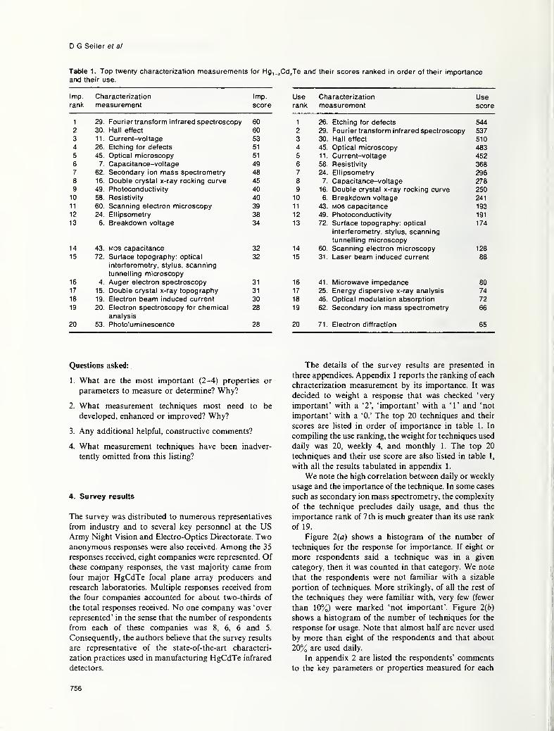
D G Seller et al
Table 1. Top twenty ctiaracterizatlon measurements tor Hg^.^^Cdj^Te and their scores ranked in order of their importanceand their use.
Imp. Characterization Imp. Use Characterization Userank measurement score rank measurement score
1 29. Fourier transform Infrared spectroscopy 60 1 26. Etching for defects 544
2 30. Hall pffprt 60 2 537
3 •) 1 1 1 tri il—viji lay
c
53 3 ijU. Mall ckffor^tnail eneci 5104 26. Etching for defects 51 4 45. Optical microscopy 4835 45. Optical microscopy 51 5 11. Current-voltage 4526 7 49 6 •JO. n^dioU VI ly 3687 62. ^oponHarv/ inn mace cnoflmmetrv 48 7 P 1 1 i ncomot r\/dlipoUillt^li y 2968 16. 45 8 7 2789 Dhntnf*nnHi i^ti\/it\/r 1 IfJlULrUI IUU<->II VI ly 40 9 lO. Double crystal x-ray rockinQ curve 250
10 58. Resistivity 40 10 6. Breakdown voltage 241
11 60. wV^Ol llllll^ dC7^^ll\^ll IIIIV^I \JO\^\J\Jj 39 11 43 193
12 24. Elllpsometry 38 12 49. Photoconductivity 191
13 6. Breakdown voltage 34 13 72. Surface topography: optical
interferometry, stylus, scanningtunnelling microscopy
174
14 43. Mos capacitance 32 14 60. Scanning electron microscopy 12815 72. Surface topography; optical
interferometry, stylus, scanning
tunnelling microscopy
32 15 31. Laser beam induced current 88
16 4. Auger electron spectroscopy 31 16 41. Microwave impedance 8017 15. Double crystal x-ray topography 31 17 25. Energy dispersive x-ray analysis 7418 19. Electron beam induced current 30 18 46. Optical modulation absorption 72
19 20. Electron spectroscopy for chemical
analysis
28 19 62. Secondary ion mass spectrometry 66
20 53. Photoiuminescence 28 20 71. Electron diffraction 65
Questions asked:
1. What are the most important (2-4) properties or
parameters to measure or determine? Why?
2. What measurement techniques most need to be
developed, enhanced or improved? Why?
3. Any additional helpful, constructive comments?
4. What measurement techniques have been inadver-
tently omitted from this listing?
4. Survey results
The survey was distributed to numerous representatives
from industry and to several key personnel at the USArmy Night Vision and Electro-Optics Directorate. Twoanonymous responses were also received. Among the 35
responses received, eight companies were represented. Ofthese company responses, the vast majority came from
four major HgCdTe focal plane array producers and
research laboratories. Multiple responses received from
the four companies accounted for about two-thirds of
the total responses received. No one company was 'over
represented' in the sense that the number of respondents
from each of these companies was 8, 6, 6 and 5.
Consequently, the authors believe that the survey results
are representative of the state-of-the-art characteri-
zation practices used in manufacturing HgCdTe infrared
detectors.
The details of the survey results are presented in
three appendices. Appendix 1 reports the ranking of each
chracterization measurement by its importance. It was
decided to weight a response that was checked 'very
important' with a '2', 'important' with a '1' and 'not
important' with a '0.' The top 20 techniques and their
scores are listed in order of importance in table 1. In
compihng the use ranking, the weight for techniques used
daily was 20, weekly 4, and monthly 1. The top 20
techniques and their use score are also listed in table 1,
with all the results tabulated in appendix 1.
We note the high correlation between daily or weekly
usage and the importance of the technique. In some cases
such as secondary ion mass spectrometry, the complexity
of the technique precludes daily usage, and thus the
importance rank of 7 th is much greater than its use rank
of 19.
Figure 2(a) shows a histogram of the number of
techniques for the response for importance. If eight or
more respondents said a technique was in a given
category, then it was counted in that category. We note
that the respondents were not familiar with a sizable
portion of techniques. More strikingly, of al! the rest of
the techniques they were familiar with, very few (fewer
than 10%) were marked 'not important'. Figure 2(6)
shows a histogram of the number of techniques for the
response for usage. Note that almost half are never used
by more than eight of the respondents and that about
20% are used daily.
In appendix 2 are listed the respondents' comments
to the key parameters or properties measured for each
756:
Hgi_j,Cd;,Te characterization measurements
Number ol Techniques (a) Number ol Techniques (b)
30
Category Category
Rgure 2. (a) Importance histogram for characterization techniques, {b) Usage histogram for characterization
techniques. In each case a minimum of eight respondents is needed to include the technique in the category.
technique. Each respondent has been identified by a
separate letter of the alphabet. Since there were 35
respondents, double letters had to be used. As can be
seen from these results, the responses for each technique
ranged from 0 to 25, a greater number of responses
usually indicating an important or frequently used
technique.
Answers to the four questions in the survey from each
respondent are presented in Appendix 3. We give
summaries of these answers in figures 3-6.
5. Summary and conclusions
To our knowledge, this is the first time such a
characterization survey has been done for HgCdTe. Webelieve that results of this survey of the importance and
prevalence of characterization techniques in the HgCdTeIR detector industry are important. We hope that they will
stimulate and challenge existing concepts and practices
and even lead to the development or application of new
characterization techniques for the HgCdTe industry.
Properties/Parameters
alloy composition (Eg,Ag)
carrier concentration
mobility
lifetime (minority carrier)
impurities (trace, etc.)
breakdown voltage
quantum efficiency
tellurium (second phase,precipitates)
crystalline quality
individual layer properties
interface/surface structure andchemistry
dark currents
1/f noise
impurity content in starting materials
defects (dislocations, etc.)
Needs for Improvement
NEED TO MEASURE PROPERTIESON SURFACE AND PROFILE IN
TO DEPTH OF SAMPLE.
NEED TO KNOWNONUNIFORMITY AND SPATIAL
VARIATIONS.
NEED SUFFICIENT KNOWLEDGETO ACCURATELY PREDICTPERFORMANCE OF REALDETECTORS.
Figure 3. Summary of most important properties or parameters to measure for HgCdTe.
757
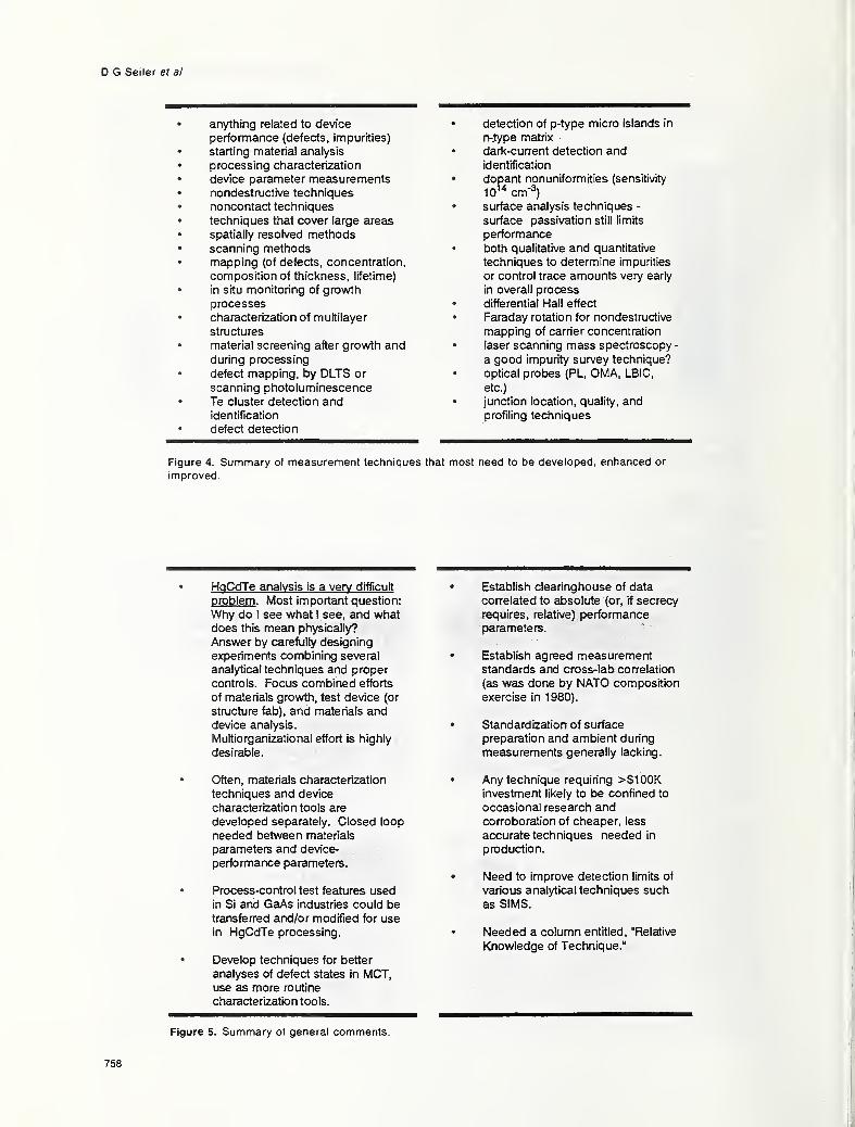
D G Seller et al
anything related to device
performance (defects, impurities)
starting material analysis
processing characterization
device parameter measurementsnondestructive techniques
noncontact techniques
techniques that cover large areas
spatially resolved methodsscanning methodsmapping (of defects, concentration,
composition of thickness, lifetime)
in situ monitoring of grow'th
processes
characterization of multilayer
structures
material screening after growth andduring processing
defect mapping, by DLTS or
scanning photoluminescence
Te cluster detection andidentification
defect detection
detection of p-type micro islands in
n-,type matrix
dark-current detection andidentification
dopant nonuniformrties (sensitivity
lO^'' cm-^)
surface analysis techniques -
surface passivation still limits
performance
both qualitative and quantitative
techniques to determine Impurities
or control trace amounts very early
in overall process
differential Hall effect
Faraday rotation for nondestructive
mapping of carrier concentration
laser scanning mass spectroscopy -
a good impurity survey technique?
optical probes (PL, OMA, LBIC,
etc.)
junction location, quality, andprofiling techniques
Figure 4. Summary of measurement techniques that most need to be developed, enhanced or
improved.
HqCdTe analysis is a very drfficult
problem . Most important question:
Why do I see what I see, and whatdoes this mean physically?
Answer by carefully designing
experiments combining several
analytical techniques and proper
controls. Focus combined efforts
of materials growth, test device (or
structure fab), and materials anddevice analysis.
Multiorganizational effort is highly
desirable.
Often, materials characterization
techniques and device
characterization tools are
developed separately. Closed loop
needed between materials
parameters and device-
performance parameters.
Process-control test features usedin Si and GaAs industries could betransferred and/or modified for usein HgCdTe processing.
Develop techniques for better
analyses of defect states in MCI,use as more routine
characterization tools.
Figure 5. Summary of general comments.
Establish clearinghouse of data
correlated to absolute (or, if secrecy
requires, relative) performanceparameters.
Establish agreed measurementstandards and cross-lab correlation
(as was done by NATO composition
exercise in 1980).
Standardization of surface
preparation and ambient during
measurements generally lacking.
Any technique requiring >$100Kinvestment likely to be confined to
occasional research andcorroboration of cheaper, less
accurate techniques needed in
production.
Need to improve detection limits of
various analytical techniques such
as SIMS.
Needed a column entitled, "Relative
Knowledge of Technique."
758 -

Hgi_^Cdj,Te characterization measurements
• Laser reflectance
• Laser microscopy• Residual stress measurements in
processed devices• Positron annihilation
• Atomic force microscopy or
scanning capacitance microscopyQuantum efficiency measurements
• Contact resistance (especially for
p-type samples)• Contact and surface recombination
velocity
Open-circuit photovoltage decayTransmission line measurements for
contact, sheet resistance
Variable-area-diode measurementsRHEED analysis
Electrochemical analysis
IR microscopy to image precipates
X-ray Laue back-reflection to
determine single crystal orientation
X-ray topography techniques other
than double crystal
Imaging SIMS
Figure 6. Summary of measurement techniques omitted from list.
CHARACTERIZATION OF HgCdTe MATERIAL
INGREDIENTSANDPROCESSING
RAWMATERIALS
SINGLEMATERIAL
MATERIALPROPERTIES
DEVICE
USES
CORRELATION CORREWTION
STRUCTUREDEFECTS
OUTPUTS OF ABOVE CYCLE BECOME INPUTS FOR CYCLE BELOW
DEVICEMATERIALSTRUCTURE
CHARACTH8ZH3MATERIALS
PROCESSES DEVICEPROPERTIES
SYSTEMUSES
CORRELATE CORRELATE
STRUCTUREDEFECTS
CHARACTERIZATION OF HgCdTe MATERIAL SYSTEMFigure 7. Diagram of the characterization activities for a single material and a material
system (see [10]). Note the strong role of characterization measurements and the need for
correlation activites.
The appendices contain all the detailed results from
the survey. Thus each person can individually interpret
and arrive at his/her own conclusions. However, the key
to success may be the adequate use and proper combination
of many of the techniques on the hst. It is worthwhile to
remember that relationships exist among the structure,
properties, synthesis, processing and performance of
HgCdTe materials and devices as shown in figure 7 [10].
Once the material properties are characterized satis-
factorily in the first part of the cycle, they become inputs
for the device cycle. Important questions need to be raised
and answered: how are the HgCdTe composition,
structure, defects and electrical/optical properties
determined by the fabrication processes, and how, in turn,
does this characterization determine the useful properties
of the electronic devices? Both scientific and technological
issues and practices need to be thoroughly understood.
Only then: (1) will HgCdTe processes and devices be
capable of being controlled and continually improved,
(2) can we hope to understand the physical mechanisms
that affect all aspects of producing HgCdTe IR focal plane
arrays, and (3) can we hope to meet the cost and reliability
requirements for HgCdTe systems.
The top five measurements in order of importance
are (1) Fourier transform infrared spectroscopy, (2) Hall
effect, (3) current-voltage, (4) etching for defects and
759
D G Seller et al
(5) optical microscopy. The top five measurements in
order of usage are exactly the same as for the importance
ranking, but with a redistribution: (1) etching for defects,
(2) Fourier transform infrared spectroscopy, (3) Hall
effect. (4) optical microscopy and (5) current-voltage.
The reasons for their high ranking can be ascertained
from the key parameters or properties they measure, as
tabulated in appendix 2. We summarize the information
obtainable from them and the reasons for their high
ranking.
For Hgi_;,CdjjTe materials, the x-value is a very
important parameter to determine because, in addition
to the temperature, it affects the energy band structure.
The energy band structure, in turn, directly affects the
cut-off wavelength, intrinsic carrier concentration, carrier
mobilities, etc. The technique used more than any other
is infrared transmission, most often called ftir for Fourier
transform infrared spectroscopy. The ftir measurement
has numerous advantages: it has mapping capability, it
is contactless and non-destructive, and it accurately
predicts cut-off wavelengths, determines layer thick-
nesses, and is thus capable of determining the x-value
and other compositional information of epitaxial layers
[11].
The Hall effect is one of the most important
characterization methods because of its wide application
in the determination of semiconductor resistivity, carrier
concentration and mobility. Discussions of the Hall effect
can be found in many solid-state and semiconductor
textbooks. It has become an excellent process monitor
for crystal growth with the purity, doping and homo-
geneity able to be correlated with growth conditions. In
addition to bulk electron and hole densities and
mobilities, one can determine inversion and accumulation
layer properties, acceptor binding energies and compen-
sation ratios from the low-temperature freeze-out of free
holes, and energy gaps from the temperature dependence
of the intrinsic carrier concentration [12].
Current-voltage measurements to determine the
behaviour of diodes are very important for characterizing
diode parameters. Two types of diodes may be distin-
guished: p-n junction diodes and metal-insulator-semi-
conductor (mis) diodes. For modern-day infrared detec-
tion the p-n junction photodiode is the more important.
Surface and geometrical effects become increasingly
important as the detector size shrinks. Bulk defects can
have impact on the operation of large arrays. Variable-
area diode data analysis is an essential tool in the
characterization of HgCdTe infrared detectors [13].
Measurement of the zero-bias resistance-area product
{RqA) and its perimeter/area dependence provides critical
information useful in separating surface and bulk effects
and evaluating the quality of the surface passivation. The
junction quality can be ascertained and the diffusion.
generation-recombination and tunnelling mechanisms
found. Leakage or dark currents, as well as breakdown
voltages, are also important parameters that can be
measured by this technique.
The physical characterization of HgCdTe crystals by
etching for defects is one of the major techniques for
measuring the deviation from perfection of the crystal
lattice. The rate of reaction of a solution with a solid
surface depends distinctly on the crystallographic orien-
tation. The rate is also significantly affected by local stress
caused by defects. Chemical etching proceeds morerapidly in regions near dislocations or any other physical
defect than in perfect regions. As a result, etch pits are
often formed on the surface. Etch hillocks may also form
and can often be confused with pits in an optical
microscope. Use of a Normarski microscope in con-
junction with preferential chemical etching and optical
microscopy is thus one of the easiest and least expensive
techniques for the determination of crystal defects in
HgCdTe. Extended crystallographic defects such as
dislocations, stacking faults, precipitates, voids and
subgrain boundaries can have a major impact on the
performance of focal plane arrays.
Finally, we note that this paper provides a reference
for the importance and use of characterization techniques
in the HgCdTe community. It should be a 'handy'
document for scientists or engineers who want to knowwhat techniques are available, what they are used for,
how important they are and how often they are used.
Acknowledgments
The authors acknowledge the partial support of this
survey by the Defense Advanced Research Projects
Agency and the US Army Night Vision and Electro-
Optics Directorate.
The authors gratefully acknowledge the invaluable
help provided by Nancy Seiler and Jane Walters in
compiling the results of this survey and the expert
assistance of Tammy Clark. Finally, many thanks are
due to the 35 respondents who took the time to fill out
the survey form.
Appendix 1. Importance and usage ranking of
characterization measurements
In this appendix the 72 characterization measurements
are ranked by their importance (table A 1) and their usage
(table A2). Note that there is generally (but not always)
a correlation between the importance rank and the usage
rank.
760
Hgi_^Cd^Te characterization measurements
Table A1. Ranking of characterization measurements by their importance.
Technique importance Use of technique
Imp.
mp. Characterization Imp. V. Imp. score Daily Weekly Monthly Use score
rank measurement I VI I + 2VI D W M 20D + 4W + M
1 29. Fourier transform infrared spectroscopy 6
2 30. Hall effect 4
3 11. Current-voltage 3
4 26. Etching for defects 9
5 45. Optical microscopy 3
6 7. Capacitance-voltage 11
7 62. Secondary ion mass spectrometry 10
8 16. Double crystal x-ray rocking curve 11
9 49. Photoconductivity 14
10 58. Resistivity 10
11 60. Scanning electron microscopy 15
12 24. Ellipsometry 12
13 6. Breakdown voltage 10
14 43. Mos capacitance 6
15 72. Surface topography: optical 14
interferometry, stylus, scanning
tunnelling microscopy
16 4. Auger electron spectroscopy 13
17 15. Double crystal x-ray topography 15
18 19. Electron beam induced current 12
19 20. Electron spectroscopy for chemical 10
analysis
20 53. Photoluminescence 12
21 67. Transmission electron microscopy 12
22 2. Atomic absorption spectroscopy 15
23 25. Energy dispersive x-ray analysis 14
24 31. Laser beam induced current 16
25 14. Deep level transient spectroscopy 15
26 61. Scanning transmission electron 11
microscopy
27 46. Optical modulation absorption 11
28 40. Mass spectrometry 12
29 12. Diode reverse recovery 11
30 13. Deep level optical spectroscopy 10
31 47. Photo Hall effect 10
32 64. Spreading resistance 7
33 8. Cathodoluminescence 14
34 71. Electron diffraction 6
35 54. Photoreflectivity 4
36 44. Neutron activation analysis 5
37 33. Low energy electron diffraction 4
38 69. X-ray photoelectron microscopy 6
39 70. Electron channelling 8
40 42. Microwave reflection 5
41 56. Raman scattering spectroscopy 7
42 57. Reflectometry 1
43 59. Rutherford backscattering spectroscopy 9
44 1. Admittance spectroscopy 4
45 3. Atomic emission spectroscopy 8
46 5. Beta-ray absorption/backscatter 4
47 21. Electroreflectance 4
48 41. Microwave impedance 2
49 17. Drift mobility 1
50 18. Eddy current 5
51 48. Photocapacitance 3
52 10. Current transient spectroscopy 6
53 65. Surface photovoltage 4
54 22. Electron energy loss spectroscopy 5
55 28. Faraday effect 5
56 32. Laser ionization mass analysis 4
57 37. Magneto-optics 2
58 68. X-ray fluorescence analysis 4
59 23. Electroluminescnce 3
60 34. Magnetoabsorption 2
27 60 26 4 1 537
28 60 25 2 2 510
25 53 22 3 452
21 51 26 4 8 544
24 51 24 3 483
19 49 12 9 2 278
19 48 1 9 10 66
17 45 11 6 6 250
13 40 8 7 3 191
15 40 18 2 368
12 39 4 10 8 128
13 38 14 3 4 296
12 34 11 5 1 241
13 32 8 8 1 193
9 32 8 3 2 174
9 31 2 2 1 49
8 31 2 4 44
9 30 1 3 3 35
9 28 2 1 5 49
8 28 5 5 25
8 28 1 1 8 32
6 27 1 5 9
6 26 2 7 6 74
5 26 3 6 4 88
4 23 3 3
6 23 1 2 22
5 21 3 3 72
4 20 1 1 7 31
4 19 2 2 48
3 16 2 1 9
3 16 3 3
4 15 1 1 3 27
14 3 3
4 14 3 1 1 65
4 12 2 1 41
3 11 1 20
3 10 1 1 24
2 10 1 1 5
1 10 2 3 11
2 9 2 1 1 45
1 9 0
4 9 3 1 64
9 2 2
2 8 2 40
8 1 1
2 8 2 0 1 41
2 8 1 1 5
3 8 4 80
3 7 1 1 1 25
1 7 2 1 1 45
2 7 1 20
6 2 1 9
1 6 0
5 1 1
5 1 1 24
4 0
1 4 1 1 5
4 1 1
3 0
2 0
{Continued)
761
D G Seller et al
Table A1. (Continued)
Imp.
rank
Characterization
measurement
Technique importance
Imp. V. Imp.
1 VI
Imp.
score
1 + 2VI
Use of technique
Daily Weekly (Vlonthly
D W MUse score
20D + 4W + M
61 38. Magnetoresistance 2 2 0
62 50. Photoelectromagnetic effect 2 2 1 1
63 51. Photoemission spectroscopy 2 2 0134 27. Extended x-ray absorption fine structure 0
65 35. Magnetoconductivity 0
66 39. Magnetophonon spectroscopy 0
67 52. Photoinduced transient spectroscopy 0
68 63. Shubnikov-de Haas effect 0
69 66. Thermal wave microscopy 0
70 9. Charged particle activation analysis 0 0
71 36. Magnetoreflectivity 0 0
72 55. Photothermal spectroscopy 0 0
Table A2. Ranking of characterization measurements by their usage.
Technique importance Use of technique
UseUse Characterization . Imp. V. Imp. score Daily Weekly Monthly Use score
rank measurement 1 VI 1 -1- 2VI D W M 20D -1- 4W -1- M
1 26. Etching for defects 9 21 51 26 4 8 544
2 29. Fourier transform infrared spectroscopy 6 27 60 26 4 1 537
3 30. Hall effect 4 28 60 25 2 2 510
4 45. Optical microscopy 3 24 51 24 3 483
5 11. Current-voltage 3 25 53 22 3 452
6 58. Resistivity 10 15 40 18 2 368
7 24. Ellipsometry 12 13 38 14 3 4 296
8 7. Capacitance-voltage 11 19 49 12 9 2 278
9 16. Double crystal x-ray rocking curve 11 17 45 11 6 6 250
10 6. Breakdown voltage 10 12 34 11 5 1 241
11 43. Mos capacitance 6 13 32 8 8 1 193
12 49. Photoconductivity 14 13 40 8 7 3 191
13 72. Surface topography: optical
Interferometry, stylus, scanning
tunnelling microscopy
14 9 32 8 3 2 174
14 60. Scanning electron microscopy 15 12 39 4 10 8 128
15 31. Laser beam induced current 16 5 26 3 6 4 88
16 41. Microwave impedance 2 3 8 4 80
17 25. Energy dispersive x-ray analysis 14 6 26 2 7 6 74
18 46. Optical modulation absorption 11 5 21 3 3 72
19 62. Secondary ion mass spectrometry 10 19 48 1 9 10 66
20 71. Electron diffraction 6 4 14 3 1 1 65
21 57. Reflectometry 1 4 9 3 1 64
22 20. Electron spectroscopy for chemical
analysis
10 9 28 2 1 5 49
23 4. Auger electron spectroscopy 13 9 31 2 2 1 49
24 12. Diode reverse recovery 11 4 19 2 2 48
25 42. Microwave reflection 5 2 9 2 1 1 45
26 18. Eddy current 5 1 7 2 1 1 45
27 15. Double crystal x-ray topography 15 8 31 2 4 44
28 5. Beta-ray absorptlon/backscatter 4 2 8 2 1 41
29 54. Photoreflectivity 4 4 12 2 1 41
30 1. Admittance spectroscopy 4 2 8 2 40
31 19. Electron beam induced current 12 9 30 3 3 35
32 67. Transmission electron microscopy 12 8 28 1 8 32
33 40. Mass spectrometry 12 4 20 1 7 31
34 64. Spreading resistance 7 4 15 1 3 27
35 53. Photoluminescence 12 8 28 5 5 25
36 17. Drift mobility 1 3 7 1 1 25
37 33. Low energy electron diffraction 4 3 10 1 24
38 28. Faraday effect 5 5 1 24
39 61. Scanning transmission electron 11 6 23 2 22
microscopy
762
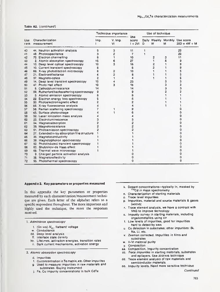
Hgi_;,Cd;,Te characterization measurements
Table A2. {continued)
Technique Importance Use of technique
UseUse Characterization Imp. V. Imp. score Daily Weekly Monthly Use score
rank measurement 1 VI 1-1- 2VI D W M 2.\j\J -T 4Vv + M
40 44. Neutron activation analysis 5 3 1
1
1 20
41 48. Photocapacitance 3 2 7 1 20
42 70. Electron channelling 8 1 10 2 3 11
43 2. Atomic absorption spectroscopy 15 6 27 1 5 9
44 13. Deep level optical spectroscopy 10 3 16 2 1 y
45 lU. Current transient spectroscopy 6 6 y
46 69. X-ray photoelectron microscopy D lU 1 (
c0
47 21. Electroreflectance A4 o0 1 1 0
48 37. Magneto-optics 2 1 4 1 1c0
49 14. Deep level transient spectroscopy 15 4 23 o O
50 4/. rnoto nail enect lU oO IDOo oo
51 8. Cathodol um i nescence 14 14 oo o
52 59. Rutherford backscattering spectroscopy 9 9 d.o£.
53 i. Atomic emission spectroscopy QO QO i1 1
54 22. Electron energy loss spectroscopy 5 541
41
55 50 Photoelectromagnetic effect o o£. 1 i
56 68. X-ray fluorescence analysis 4A4
A\
•A
1
57 56. Raman scattering spectroscopy 7 1 yftU
58 65. Surface photovoltage 4 1 t3ftU
59 32. Laser ionization mass analysis 4 4 ftu
60 23. Electroluminescence 3 oftu
61 34. Magnetoabsorption lio ftu
62 38. Magnetoresistance i. d.ftu
63 51. Photoemission spectroscopy 2ftu
64 27. Extended x-ray absorption fine structure 0
65 35. Magnetoconductivity 0
66 39. Magnetophonon spectroscopy 0
67 52. Photoinduced transient spectroscopy 0
68 63. Shubnikov-<Je Haas effect 0
69 66. Thermal wave microscopy 0
70 9. Charged particle activation analysis 0 0
71 36. Magnetoreflectivity 0 0
72 55. Photothermal spectroscopy 0 0
Appendix 2. Key parameters or properties measured
In this appendix the key parameters or properties
measured by each characterization/measurement techni-
que are given. Each letter of the alphabet refers to a
specific respondent throughout. The more important and
highly used the technique, the more the responses
received.
1. Admittance spectroscopy
t. (On MIS) A/js, flatband voltage
w. Conductance
dd. Deep level analysis
ff. Interface state density
hh. Lifetimes, activation energies, transition rates
ii. Dark current mechanisms, activation energy
2. Atomic absorption spectroscopy
d. Impurities
f. Cu concentration in Te matrix, etc. Other impurites
g. Used to measure impurities in raw materials and
substrates. Buying instrument
j. Fe, Cu impurity concentrations in bulk CdTe
k. Dopant concentrations—typically In, masked by
"^Cd in mass spectrometry
n. Characterization of starting materials
o. Trace level impurities
p. Impurities, material and source materials & gases
(MOCVD)
r. Trace element analysis, we have a contract with
VHG to improve technology
s. Impurity survey in starting materials, including
organometallics using icp
t. Low levels of impurities, good for impurities
hard to detect by sims
u. Cu detection in substrates; other impurities: Si,
Na, Li, etc.
V. Zeeman corrected. Impurities in films and
substrates
w. II-VI material purity
y. Composition
aa. Composition, impurity concentration
cc. Trace impurities in starting materials, substrates
and epilayers. Use zcgfaas technique
dd. Trace element analysis of raw materials and
semiconductor materials
ee. Impurity levels. Need more sensitive technique
Continued
763
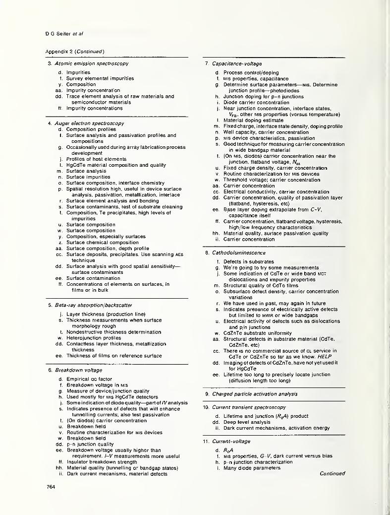
D G Seller et al
Appendix 2 (Continued)
3. Atomic emission spectroscopy
d. Impurities
f. Survey elemental Impurities
y. Composition
aa. Impurity concentration
dd. Trace element analysis of raw materials andsemiconductor materials
ff. Impurity concentrations
4. Auger electron spectroscopy
d. Composition profiles
f. Surface analysis and passivation profiles andcompositions
g. Occasionally used during array fabrication processdevelopment
j. Profiles of host elements
I. HgCdTe material composition and quality
m. Surface analysis
n. Surface impurities
o. Surface composition, Interface chemistry
p. Spatial resolution high, useful In device surface
analysis, passivation, metallization, interface
r. Surface element analysis and bonding
s. Surface contaminants, test of substrate cleaning
t. Composition, Te precipitates, high levels of
impurities
u. Surface composition
w. Surface composition
y. Composition, especially surfaces
z. Surface chemical composition
aa. Surface composition, depth profile
cc. Surface deposits, precipitates. Use scanning aes
technique
dd. Surface analysis with good spatial sensitivity
—
surface contaminants
ee. Surface contamination
ff. Concentrations of elements on surfaces, in
films or in bulk
5. Beta-ray absorption/backscatter
j. Layer thickness (production line)
s. Thickness measurements when surface
morphology rough
t. Nondestructive thickness determination
w. Heterojunctlon profiles
dd. Contactless layer thickness, metallization
thickness
ee. Thickness of films on reference surface
6. Breakdown voltage
d. Empirical QC factor
f. Breakdown voltage in mis
g. Measure of device/junction quality
h. Used mostly for mis HgCdTe detectors
j. Some Indication of diode quality—part of /l/analysis
s. Indicates presence of defects that will enhancetunnelling currents; also test passivation
t. (On diodes) carrier concentration
u. Breakdown field
V. Routine characterization for mis devices
w. Breakdown field
dd. p-n junction quality
ee. Breakdown voltage usually higher than
requirement. I-V measurements more useful
ff. Insulator breakdown strength
hh. Material quality (tunnelling or bandgap states)
ii. Dark current mecanlsms, material defects
7. Capacitance-voltage
d. Process control/doping
f. MIS properties, capacitance
g. Determine surface parameters
—
mis. Determinejunction profile—photodlodes
h. Junction doping for p-n junctions
I. Diode carrier concentration
j. Near junction concentration, interface states,
VpB. other mis properties (versus temperature)
I. Material doping estimate
m. Fixed charge, Interface state density, doping profile
n. Well capacity, carrier concentration
p. MIS device characteristics, passivation
s. Good technique for measuring carrier concentration
in wide bandgap material
t. (On MIS, diodes) carrier concentration near the
junction, flatband voltage, N^^
u. Fixed charge density, carrier concentration
V. Routine characterization for mis devices
w. Threshold voltage; carrier concentration
aa. Carrier concentration
cc. Electrical conductivity, carrier concentration
dd. Carrier concentration, quality of passivation layer
(flatband, hysteresis, etc)
ee. Base layer doping extrapolate from C-V,capacitance Itself
ff. Carrier concentration, flatband voltage, hysteresis,
high/low frequency characteristics
hh. Material quality, surface passivation quality
ii. Carrier concentration
8. Cathodoluminescence
f. Defects in substrates
g. We're going to try some measurementsj. Some indication of CdTe or wide band mct
dislocations and impurity properties
m. Structural quality of CdTe films
0. Subsurface defect density, carrier concentration
variations
r. We have used in past, may again in future
s. Indicates presence of electrically active defects
but limited to mwir or wide bandgapsu. Electrical activity of defects such as dislocations
and p/n junctions
w. CdZnTe substrate uniformity
aa. Structural defects in substrate material (CdTe,
CdZnTe, etc)
cc. There is no commercial source of cl service in
CdTe or CdZnTe so far as we know. HELPdd. Imaging of defects of CdZnTe, have not yet used it
for HgCdTeee. Lifetime too long to precisely locate junction
(diffusion length too long)
9. Charged particle activation analysis
10. Current transient spectroscopy
d. Lifetime and junction (R^) product
dd. Deep level analysis
ii. Dark current mechanisms, activation energy
11. Current-voltage
d. RqAf. mis properties, G-V, dark current versus bias
h. p-n junction characterization
1. Many diode parametersContinued
764
Hg,_,Cd^Te characterization measurements
Appendix 2 (Continued)
j- Provides key insignt botn into diode performanceano incundiiioiiio \vcr5us lemperaiure^
1
m
.
L-caKayc ouiiciii, udiK curreni in pnoiouioues
P- Key device performance parameters, RqA etc for
pnOlOVOIlalC OIOQc
r. Diode IV characteristics
s. nyH, uicai\uuwii vuiidyc, piiuiuoui rcmt (On diodes) origin of lealoQe currents
u. RcAw.
aa. Diode properties
dd. Junction quality
ee. /?(,, Ra(V), /?series Model diffusion, G-R. andtunnelling mechanisms
ff. RqA. leakage current
hh. Dark current mechanisms, breakdown properties
11. Dark current mechanisms, activation energy
12. Diode reverse recovery
d. Lifetime after diode processing
g- OMA and pc-rolloff to determine lifetime
h. Carrier lifetime
i. Minority carrier lifetime
j- Some idea of minority carrier lifetime near junction
(versus temperature)
1. Diode lifetime
m. Minority carrier lifetime
t. Lifetime in depletion region
aa. Diode properties
dd. Recombination lifetime in diode; difficult for thin-
base diodes
ee. Lifetime
ii. Lifetime, activation energy
Deep level optical spectroscopy
d. Check on process, deep levels, not routine
(simpler than dlts)
m. Defect density, energy level and capture cross
section
r. Optical determination of impurity levels
s. Midgap states
t. Deep levels
cc. Nature of traps
dd. Deep level analysis
ee. Ej
ff. Energy of trap levels
ii. Activation energy
14. Deep level transient spectroscopy
d. Check on process, deep levels, not routine
f. Au in Si and GaAsm. Defect density, energy level and capture cross
section
n. Impurity levels
r. Looks at impurity, vacancy levels. Seemsproblematic for hct
s Midgap states, levels and concentrations
t. Deep levels
V. Desirable to correlate with device performance
w. Traps in wide bandgap ll-VI materials
dd. Deep level analysis
ee. Trap levels, cross sections (expensive to
use)
ff. Energy of trap levels
gg Defect levels
ii. Activation energy
15. Double crystal x-ray topography
d. Defects—much too time-consumingi. Defects
j. Some insight into defects and strain
k. Cd(Zn)Te(Se) substrate quality (substructure,
inclusions, precipitates)
m. Structural quality over large areas
n. Crystalline perfection
p. Crystal quality bulk substrates
r. Surface topograph
s. Spatial variations in crystal quality
t. Spatial structural uniformity, defect structure
u. Crystalline perfection, precipitates, dislocation
types and arrangementv. Crystal perfection—films and substrates
w. Structural perfection of ll-VI materials
y. Surface roughnesscc. Crystal perfection, defect topography
dd. High resolution imaging of defect strain field
ee. Surface crystal lattice quality
16. Double crystal x-ray rocking curve
d. FWHM of epilayers and substrates
g. Determine quality of layer, crystallinity and lattice
matching with substrates
i. Crystal quality
j. Basic crystal quality of epi
I. Substrate quality; substructure, dislocations
m. Structural quality of CdTe and HgCdTe layers
n. Subject to interpretation
p. X-tal quality of epi
r. Wo have a Brimrose X-ray mapper. It producesboth topographs and rwhm rocking curve maps
s. Crystalline quality of epilayers, tilt, strain,
composition, dislocation density
t. Crystallinity
u. Microstructures/grain boundaries, etc.
V. Crystal perfection—films and substrates
w. Structural perfection of ll-VI materials
y. Structural perfection
z. Crystal lattice perfection
aa. Structural properties/crystal quality
cc. Gives number related to crystal perfection. Mustbe in conjunction with x-ray topography or etch
pitting
dd. Crystal quality, fwhm of substrates and epitaxial
layers, lattice mismatchee. Crystal quality
ff. Linewidth, crystalline perfection
gg. Crystalline defects
hh. Epilayer quality, substrate quality
17. Drift mobility
j. Basic to assessing materials electrical properties
(versus temperature and field)
m. Minority carrier mobility for photoconductors
ee. Mobility
18. Eddy current
f. Electrical conductivity
V. Non-destructive measurement of conductivity in
films
w. Measure lpe liquidus
cc. Electrical resistivity
ee. Resistivity (no instrumentation readily available)
ii. Carrier concentration
Continued
765
D G Seller et al
Appendix 2 {Continued)
19. Electron beam induced current
d. Investigation of junction location; check on BADdevices on fpas in certain configurations
f. Diffusion lengths, electrically active defects,
mapping, junction depths
g. Location of electrical versus metallurgical junction
i. Junction position
]. Junction depth, hidden junctions
m. Diode junction location, diffusion length
o. Subsurface defect structure, junction depth
s. Indicates junction location and electrically
active defects
t. Junction depth in diodes
u. p/n junction depth
w. Type variations in HgCdTedd. p-n junction location on cleaved diodes
ee. Electrically active defect mapping, junction
location, x-value, limited spatial resolution
hh. Diode contours, junction profiles
li. Electrically active defect
20. Electron spectroscopy for chemical analysis
f. Passivation compositions
g. Used during process development to obtain
chemical information (residue after etching,
etc.)
j. Helps assess surface contamination and processes
I. HgCdTe material
n. Material analysis
o. Surface and interface chemistry
p. Chemical surface and interface information.
Compound formation during epi growth,
metallization, etc, non-destructive depth profile
MBE interface, electronic parameters
r. Use along with Augert. Surface chemistry
w. Surface analysis—cleanups, passivations
z. Surface chemical constituents
cc. Surface chemistry, surface deposits
dd. Surface analysis of insulators; HgCdTe composition
depth profile, interface between insulator/
semiconductor
ee. Surface contamination
ff. Chemical composition of surfaces and films
21. Electroreflectance
j. Tells something about surface composition andproperties, but not too clear how useful
I. HgCdTe composition
n. Results questionable' s. X profile with depth
t. Composition, E^, Aq, crystalllnity
aa. Composition, bandgapdd. Composition, carrier concentration if calibrated.
Requires ohmic contact to sampleee. MCT x-value
ff. Bulk composition from E^, material quality from
linewith FII. Composition, maybe carrier concentration
22. Electron energy loss spectroscopy
o. Low Z element surface analysis, electronic
states and chemical bonding
s. Bonding of surface atomsdd. Used in tem analysis to determine composition
ee. Surface crystal diffraction patterns
ff. Vibrational energies of phonons and adsorbates(high resolution mode)
23. Electroluminescence
d. Check on junction quality
t. (p-n junctions) radiative quantum efficiency
ee. More useful in other material systems
24. Ellipsometry
g. Thin film thicknesses and index, mct surface state
h. Surface preparation monitor for various parts of
processes
j. Tells surface condition, composition, film structures
m. Film quality in detector. Passivation
n. Film thickness and uniformity
p. Non-destructive mbe growth control
r. Optical constants, film thickness
s. X profile with depth, measure dielectric layers
t. Surface conditions, bandgapu. Index of refraction for insulators. (Not useful for
MOT?)
w. Surface cleanliness, film thickness
y. >p and A, n, film thickness
z. Substrate surface contamination
dd. Excellent measure of surface cleanliness
ee. Surface cleanliness, film thickness
ff. Film thickness and refractive Index
hh. Surface quality, surface contamination
25. Energy dispersive x-ray analysis
f. LPE compositional profiles
g Occasionally used during process development.
Would use more if had a good in-house one
j. Gives gross confirmation of compositional profiles
m. Determination of X-value in HgCdTe layers
o. X-value, compositional uniformity
p. Film composition average, e.g. X-value
r. Maps of wafer X-value, impurity mapss. Composition analysis in thick films
t. Compositions and their depth profile
w. Chemical mapping on devices
y. Composition
z. Layer composition
aa. Composition
cc. Chemical nature of precipitates, Zn % czt,
chemistry of deposits
dd. Destructive measure of composition; routine for
failure analysis of processing problems
ee. 'Bulk' composition and impurities
ff. Bulk composition of Hg,_^Cd;,Te
26. Etching for defects
d. Defects
f. Dislocation and Te precipitate density
g. Qualify substrates and check growth process
i. Defects
j. Tells dislocation density of layer—essential to
materials improvementk. Te precipitates, dislocations, substructure
(orientation A/B)
m. Indirect assessment of crystalline quality
o. Etch pit density
p. Defect measure, substrate film
r. We don't do this, but others use a lot for material
dislocation density
s. Dislocation density
t. Defect structure, epd
u. Dislocations, Te precipitates
Continued
766
Hgi_j,Cdj,Te characterization measurements
Appendix 2 (Continued)
V. Dislocations—pits—inclusions in films andsubstrates
w. Dislocation density In HgCdTe and CdZnTe. Damagey- Etch pit density, A-B face (111)
z. Crystal lattice perfection
aa. Defects (structural)
cc. Defect densities, dislocation nature anddistribution
dd. Best technique available for determiningdislocation density
ee. Correlation of etch defects with device performanceff. Dislocation density, substructure
hh. Material quality, dislocations and other defects
ii. Dislocations, microstructure
27. Extended x-ray absorption fine structure
28. Faraday effect
f. Local carrier concentration
u. Is this rotation?
w. Carrier concentration In HgCdTeff. Carrier concentration
gg. Carrier concentration (under development)hh. Material uniformity, Nq — N/^
ii. Carrier concentration
29. Fourier transform infrared spectroscopy
d. Cutoff, thickness
f. Cutoff measurementsg. Measure transmittance of substrates, films,
determine X-value, device spectral response
h. Film cut-off and thickness from ir transmission
spectrum. Device cut-off wavelengths andspectral response
i. Composition
j. Gives composition of film, spectral response
(temperature dependence important)
k. Composition determination, ir transmission
I. Diode spectral response
m. X-value, thickness. We use double beam ir grating
spectrophotometer
n. Composition, uniformity
p. Key performance parameters, absorption a
s. Composition and thickness mappingt. Composition, gradients, thickness, far ir for
transport
u. Composition (from bandgap), thickness, scattering
v. Cut-oH wavelength and thickness in mct films
w. Epilayer thickness, cut-off wavelength
y. Molecular (group) vibrational modesaa. Cut-on k. thickness, free-carrier absorption
cc. IR transmission, Impurity effects or stoichiometric
deviations
dd. Accurate, nondestructive mapping of mct
composition
ee. X-value, transmission
ff. Cutoff wavelength/composition uniformity
gg Composition
hh. Energy gap for grown material
ii. Composition, carrier type? (below bandgapabsorption)
30. Hall effect
d. Transport properties
f. Material type and carrier concentration, mobility
g. Process monitor for crystal growth. Carrier density
and mobility
h. Versus magnetic field is ESSENTIAL!! Versustemperature is desirable. With resistivity, gives
carrier concentration and mobility. Multiple
carrier effects must be taken into account in
many cases1. Carrier concentration/mobilities
j- Gives essential layer electrical properties
(profile and versus B and T)
k. Electrical parameters—purity, doping, homogeneity1. Material doping
m. H, n, /?n, resistivity
n. Carrier concentration, mobility
P- Type determination, doping, carrier behaviour
r. Carrier type, concentration mobility. Use dependson facilities and demand
s. Carrier concentration and mobility
t. n, n, pu. /Vjj, mobility, type
V. Electrical properties in mct films
w. Carrier concentration, mobility, type
aa. Carrier concentration, mobility, resistivity
cc. Bulk chemistry effects, impurities, process
variations
dd. Destructive measurement of carrier concentration,
mobility, resistivity
ee. IJL, Nf^, Nq (versus 7" and versus H)ff. Carrier concentration, mobility
gg- Carrier concentration (mobility)
hh. Material type, carrier concentration, mobility;
homogeneity Indicator
ii. Carrier concentration
31. Laser beam induced current
d. Use on FPC diodes restricted to certain configura-
tions. Can only evaluate drastic failure
f. Variations in electrically active defects
g Identify active areas and location of 'breakdown'
i. Electrical uniformity
j- Helps assess material quality, junction location,
optical area, etc
m. Diode junction location, diffusion length
0. Defect features
s. Junction location, electrically active defects
t. Electrically active defects, qe of diodes
u. p-n junctions in uniform mct
w. Uniformity of HgCdTe, junction profiles
dd. Difficult to interpret results on n-type material
—
requires contacts to sampleee. Defect mapping
ff. Implant uniformity, carrier inhomogeneity, diode
junction position
gg- Electrically active (charged) defects.
inhomogeneities
hh. Homogeneity of type of material; diode
contours
ii. Electrically active defect, minority carrier diffusion
length
32. Laser ionization mass analysis
f. Impurity analysis
i-Possibly better than sims for certain elements
s. Microanalysis of precipitates
z. Impurity concentrations
aa. Impurity
cc. Specialized impurity analysis. Might offer somelower detection limits
dd. Quantitative trace-level analysis
ee. Use SIMS instead
{Continued)
767

D G Seller et al
Appendix 2 (Continued)
33. Low energy electron diffraction
i. In situ monitoring of mbe growth
s. Surface crystalline structure
t. Surface chemistry, lattice spacing
y. Surface atomic order or disorder
dd. Used as a measure of surface cleanliness andcrystallinity primarily in mbe
ee. Surface crystal quality and lattice parameters, goodfor MBE
34. Magnetoabsorption
h. Research technique to obtain fundamental material
properties
r. Good technique for looking at impurity levels,
carrier lifetime. We have no facilities for this nows. Fine structure
w. Defect and impurity states in HgCdTedd. NIST accurate determination of mct bandgap
versus composition and temperature
35. Magnetoconductivity
h. Research technique to obtain fundamental material
properties
r. Good technique for looking at impurity levels,
carrier lifetime. We have no facilities for this nows. Fine structure
36. Magnetorefiectivity
h. Research technique to obtain fundamental material
properties
r. Good technique for looking at impurity levels,
carrier lifetime. We have no facilities for this nows. Fine structure
37. Magneto- optics
h. Research technique to obtain fundamental
material properties
r. Good technique for looking at impurity levels,
carrier lifetime. We have no facilities for this nowhh. Bandgap states investigations. Spectroscopy,
transition rates
ii. Activation energy
38. n/lagnetoresistance
h. Research technique to obtain fundamental material
properties
r. Good technique for looking at impurity levels,
carrier lifetime. We have no facilities for this nowii. Carrier type
39. Magnetophonon spectroscopy
h. Research technique to obtain fundamental
material properties
r. Good technique for looking at impurity levels,
carrier lifetime. We have no facilities for this nows. Coordination and short-range ordering in alloy
40. l\Aass spectrometry
f. Impurities, dopant profiles
g. Monitoring high vacuum processes
j. Gives basic purity information on solid source
material
k. Low discharge mass spectrometry is routine purity
control
n. Chemical analysis
o. Major constituent and impurity analysis
p. Impurities of source materials
r. Regularly used to look at film junctions,
interdiffusion, impurities
s. GCMS of starting materials can analyse for
organic impurities
t. Very important with sims
w. II-VI material purity
y. Trace elements
z. Impurity concentrations
aa. Trace impurity
cc. Glow discharge MS and spark source MS are goodimpurity screening techniques but do not give
low enough dls. icpms has proved very poor in
CT and czT matrices
dd. Trace impurity analysis
ee. Impurity levels
ff. Background gas composition, primary gascomposition
41. Microwave impedance
f. Conductivity
u. Minority carrier lifetime
w. Lifetime
dd. Contactless resistivity measurementee. Lifetime
hh. Carrier lifetime
42. Microwave reflection
d. Lifetime
f. Lifetime measurementsg. Tried some measurements with inconclusive
results
t. Minority carrier lifetime
V. Minority carrier lifetime in mct films
dd. Contactless measurement of carrier lifetime
ee. Lifetime
ff. Minority carrier lifetime
hh. Carrier lifetime
43. MOS capacitance
f. Carrier concentration, cut-off, storage time,
breakdown voltage, etc
g. Surface passivation quality; fixed charge andsurface states
h. Monitor fixed charge at interface; measure dopant
concentration
i. Surface
j. Basic information on flat band—important to
understanding surface properties
I. ZnS/HgCdTe passivation quality and material
doping
m. Insulator thickness
s. Storage capacity of mis devices or persistent
currents in diodes
t. Carrier concentration, flatband voltage, N^^
w. Carrier concentration
dd. Surface passivation quality, carrier
concentration
ee. Surface states, surface charge: process monitor for
passivation
ff. Insulator thickness and uniformity
hh. Material quality, surface quality
ii. Carrier concentration—activation energy (dlts)
44. Neutron activaton analysis
f. Residual impurity analysis
k. Special (im)purity analyses
Continued
768

Hgi^Cd^Te characterization measurements
Appendix 2 [Continued)
m. Impurity determination
n. For tellurium and cadmium analysis
w. Impurities in ll-VI materials
cc. Good for a very few impurities in ct/czt materials,
but it has excellent dls when applicable
dd. Trace impurity analysis
ee. Impurity determination (level)
ff. Elemental composition
45. Optical microscopy
d. Need automated scanning of morphology with
macro-micro resolution (sampling micro)
f. Dislocation and precipitate densities, micro-
structure of bulk MCT, defects, morphologyi. Morphology
j. Essential to observation of defects, layer thickness,
crystal morphology and growth features
k. Surface quality
I. Fabrication and material defects
m. Surface morphology, defect determination,
thickness
p. General structure of materials and devices
r. Inspection of devices and materials, ir microscopeis also useful
s. Surface morphology, macro-defect density
t. Surface roughness, macro-defects
u. Surface morphology
y Surface features
z. Surface morphologycc. Manyfeatures of surfaces, cleaved cross sections,
damage features
dd. Surface inspection/characterization
ff. Defect density
46. Optical modulation absorption
d. Accurate low temperature cut-off; contactless
lifetime measurements; measure of junction
RqA in LWiR
g. Lifetime measurements, cut-off measurements,wafer level screening
h. Lifetime; device cut-off wavelength; film quality
j. For T
I Heterojunction material cut-off, response time
m. X-value
o Carrier lifetime
t. Nilinority carrier lifetime, defect levels
w. Lifetime
dd. Contactless carrier lifetime measurement andmapping
ee. Bandgap, lifetime
ff. Carrier concentration
hh. Carrier lifetimes
ii. Lifetime
47. Photo Hall effect
i. Properties of minority carriers
j. For mmority t, /j
m. Influence of compensation on mobility
s. Surface states
t. N^.N^u. Type, donor and acceptor concentration, mobility
hh. Lifetime measurements, transport data versus
temperature, etc
ii. Activation energy, trap levels
48. Photocapacitance
s. Surface states
t. Defect levels
w. Detectors
ee. Used in the past with mis structure to screen wafers
<or
ii. Quantum efficiency, responsivity
49. Ptiotoconductivity
f. Lifetime
g. Photoconductive devices
h. Carrier lifetime
i. Transients for minority carrier lifetime
j. Lifetime and essential to materials/device
understanding
k. Predictor of pc response—used on bulk cmt and epi
EMT
m. Lifetime
p. Lifetime measurementsr. Pulse decay lifetime measurements for material
lifetime and surface recombination
s. t\/1inority carrier lifetime
t. Minority carrier lifetime, PC decay on diodes gives
w. Detectors, lifetime
cc. Might correlate to purity and stoichiometry
dd. Carrier lifetime measurement (transient)
ee. Lifetime pc device
ff. PC lifetime
gg. Lifetime
hh. Material quality, spectral response, lifetimes
ii. Lifetime, surface recombination velocity
50. Photoelectromagnetic effect
ee. Device parametershh. Minority carrier versus majority carrier effects
51 . Photoemission spectroscopy
s. Bonding of dopants and impurities
w. Surface analysis
ff. UPS—measures valence electron energies; xps—see ESCA
52. Photoinduced transient spectroscopy
cc. Traps and defects, impurities, and the way they
are tied up in materials
dd. Needs development work
53. Photoluminescence
d. Compositions/lifetimes (77 K)—this technique Is
definitely underutilized in epilayer. Also
substrate evaluation of low temperature 4 K
g. Compositional measurementh. Carrier lifetime; surface quality
j. Provides some useful information on CdTesubstrate quality
m. Measure crystalline quality of CdTe epi
n. Characterization of substrates
p. Non-destructive electronic characteristics
measurementss. Important for wide bandgap (defects, impurities, etc)
t. Non-radiative centres (distribution), shallow levels,
Te precipitates
u. Very useful for substrates (Cd, Zn)Te. Acceptor
levels/donor levels/£g/[Zn] concentration
w. Wide-gap ll-VI materials purity and defects
z. Impurities
aa. Impurities, composition, crystal quality
cc. Optically active impurity and defect states; effect of
various annealing treatments
Continued
769

D G Seiler et al
Appendix 2 {Continued)
dd. Primarily used to determine composition of
CdZnTe (77 K meas. temp.)
ff. CdTe perfection
hh. Material quality, defect bands, particularly
epilayers
54. Photoreflectivity
d. MoreaccuratesurfaceX-values. Alsosurfacestate
evaluation
p. Film composition, X-value, non-destructive mbegrowth control
r. HCT X-value at the surface; formerly used frequently,
equipment currently downs. Alloy composition
t. Composition, E^, £2, Aq, crystallinity
aa. Surface composition
dd. Contactless compared with electroreflectance
ff. Composition (X-value)
ii. Composition—carrier concentration?
55. Photothermal spectroscopy
56. Raman scattering spectroscopy
\. Tried to get surface information (not sensitive).
Bulk information not clear as to importance
p. Crystal lattice quality and imperfections
t. Te precipitates, composition
w. Clustering in ll-VI materials
y. Molecular species, group vibrations
dd. Surface ordering, not much work done for hot
ff. Vibrational modes of compoundsIi. Phonon energies, defects? (anti-site)
57. Reflectometry
g. uv-vis reflectance used to determine X-value
h. Reflectance spectrum near the and -1- A,
transitions. Gives x at the surface
s. Alloy composition
dd. uv reflectance (£, transition) used to map surface
composition of mct (300 K meas.)
ee. Surface X-value
58. Resistivity
d. Part of Hall process
f. Hall measurements, determination of p-type
material
g. Part of Hall measurementi. With Hall for cc and nj. With Hall, gives mobility—essential to materials,
understanding and device modelling
k. Electrical parameters (with Hall)—purity,
doping, etc
m. Carrier concentration, contact resistance
s. Deduce mobility in conjunction with Hall
measurements, contact resistance
t. Product of carrier concentration and mobility
w. HgCdTe for photoconductors
cc. Impurities, defects, stoichiometry, annealing effects
and effectiveness
dd. Integral part of Hall effect measurements: not
separately measuredee. Done in conjunction with Hall effect
ff. Resistivity of metal film or semiconductor
gg. Mobility
hh. Material type, carrier concentration mobility;
homogeneity indicator
59. Ruttterford backscattering spectrometry
f. Passivation characterization and implant profiling
j. Provides information on near-surface composition
and damagem. Chemical analysis, crystal perfection
s. Composition depth profiles, crystallinity and strain
y. Atom %dd. Crystallinity of epitaxial layers, ion implantation
damage, etc
ee. Passivation layer purity (hard to use for mct)
ff. Film composition, density
60. Scanning electron microscopy
d. Morphology
g. Important for process development
j. Key to detailed morphology examination
I. Fabrication/material analysis, especially defects
m. Surface imaging, defects
n. Defects
o. Morphology, crystalline quality, chemical
composition, etc
p. Surface features
r. Used for materials and device inspection
s. Morphology, layer thickness
t. Morphologyu. Surface morphology, composition by wdx, edax
V. Surface defects and other features
w. Device examination
y. Microstructure
z. Surface morphology, crystallinity, thickness
cc. Surface damage, surface features, surface deposits
dd. Routine characterization of materials and devices
ee. Structural micro-features
ff. Step coverage, surface morphology
61. Scanning transmission electron microscopy
f. TEM of defects
g- Locating inclusion, dislocations, etc
m. Dislocation density
n. Defects
P- Interface structure
t. Defect structure
y- Defect structure
dd. Presently use tem only
ee. Defects. Difficult to use
ff. Presence of dislocations, twinning
hh. Defect quality of material, interfaces
62. Secondary ion mass spectrometry
d. Impurities
f. Chemical analysis of dopant profiles andimpurities
g. Determine impurity locations, dopant versus
X-value profiles
h. lpe film composition and impurity profiles
i. Impurities
j. Key to materials purity and composition and
interface control
I. HgCdTe heterostructure material composition,
impurities
m. Impurity determination
n. Analysis of impurity clusters
p. Impurity doping profiles
r. Regularly used to look at film junctions,
interdiffusion, impurities
s. Impurity analysis and depth profiles
t. Impurity concentration (profiles), composition
Continued
770
Hg,_j,Cd^Te characterization measurements
Appendix 2 {Continued)
u. Measure concentration of various impurities in motand (Cd. Zn)Te
w. Impurities in II—VI materials
y. Trace elemental analysis
2. Impurity concentration
CC, Depth profiling of trace impurity and dopantconcentrations, interface or surface pile-ups,
segregation effects
dd. Trace level analysis, doping profiles
ee. Impurity levels
ff. Elemental composition, implant depth
gg Profiling of impurities, and composition
63. Shubnikov-de Haas effect
s. Interface states and band bending
64. Spreading resistance
g Important for fpa (staring)
h. Gives contact resistance
j- Spatial information
1. Use trans, line method contact resistance
s. Sheet resistance
t. Transport, n^ product
w. Conductivity uniformity
dd. 77 K spreading resistance technique to profile p-n
junctions needs development!
ee. Use to analyse contact resistance
65. Surface photovoltage
d. Carrier concentration;
r. We have used optical scanning technique in
conjunction with electrical contacts to seephotovoltaic and photoconductivity
response
dd. Not yet developed for mct, requires contacts onsamples
ii. Carrier type changes (inhomogeneity)
66. Thermal wave microscopy
j- Tried, but found nothing after a casual look
m. Defect imaging
67. Transmission electron microscopy
f. Defect analysis and microstructural analysis
j- Key insight into materials defects
m. Dislocation density determination
n. Defects, dislocations
P Interface structure local phasess. Analysis of defects
t. Defect structure
V. Defect analysis
w. Precipitates, dislocation structure, interface in
ll-VIs
y- Defect structure
2. Defect structure
CC. High magnification defect and dislocation analysis,
damage structure
dd. Imaging of structural quality of thin-film interfaces
in cross section
ee. Defects, structure. Difficult to useff. Crystalline quality
hh. Defect quality of material interfaces
68. X-ray fluorescence analysis
m. Impurity determination
t. Composition
u. Not very sensitive
y. Atom %dd. Composition measurement of large-area
samples
69. X-ray photoelectron microscopy
f. Surface contamination on thin film profiles
I. HgCdTe material composition, impurities
p. Local device chemistry; information on films andinterfaces
r. SEM in this mode gives greater sensitivity for
elemental analysis
s. Analysis of Impurity bonding
y. Composition
dd. Surface composition analysis; combined with
sputtering can be used for comp. depth profiling,
interface chemical composition
70. Electron cfiannelling
d. Orientation; surface preparation
0. Orientation, near surface crystalline quality
p. Rough orientation of crystal films
s. Crystallinity of thin layers
y. Structural symmetryz. Crystal orientation and perfection
dd. Rapid surface sensitive measurement of
crystallinity (qualitative)
71. Electron diffraction
f. MBE growth, crystal quality and orientation
j. Essential to good mbe
p. Assume rheed, growth monitor mbe
s. In conjunction with tem for analysis of defects
t. Lattice spacing, crystallinity
u. Crystalline quality, orientation. Burger's vector
y. Order/disorder
dd. Useful in high-vacuum environments such as i^be
ff. Surface perfection in mbe
72. Surface topography: optical interferometry, stylus,
scanning tunnelling microscopy
d. Topography; defects
f. Nomarski interference microscopy, to see shallow
etch pit defects
g. Thin film process measurements, grown lpe film
surface morphology
j. Helps get film thicknesses, wafer depths
n. Uniformity
p. Topography to calibrate film thickness, roughness,
device structures, depth analysis craters, atomic
resolution structure, electronics of surface and
Interface, epi films, non-destructive device
testing
r. Make interferometric topographs. May use to
measure thickness of films by looking at bevelled
edge of multilayer structure, and detecting
transitions by phase change
s. Measurement of surface topography, height andperiod
w. Wafer flatness
y. Roughness at various levels of scrutiny to atomic
resolution
CC. Surface flatness of substrates
dd. Fizeau—flatness; Stylus—etch depths, surface
roughness, etc; stm—not widely used in mct (need
clean surfaces)
ff. Film thickness; stress from bow measurement
771

0 G Seller et al
Appendix 3. Results from questions asked
In this appendix we tabulate the answers given by the
respondents to four questions asked. Again each letter
of the alphabet refers to a specific respondent throughout
this appendix, as in appendix 2.
Questions
1. What are the most important (2-4) properties or
parameters to measure or determine? Why?
a. Bandgap, carrier concentration. Hall
mobility, dislocation density, lifetime
c. Carrier concentration, X^, uniformity, charge
storage
d. Cut-off/composition, carrier concentration,
Hfetime, RqAe. Diode l-V, Hall, spectral response
f. Voltage past threshold (breakdown voltage),
storage time, cut-off wavelength. Hall
carrier concentration and mobihty,
dislocation density, mis performance
g. Where are the leakage currents? Surface or
bulk? Are they locaHzed defect: Substrate
related?
Properties of the individual layers of
heterostructure material
h. Hgi_^Cd^Te alloy composition, carrier
concentration, carrier lifetimes, carrier
mobilities. These directly determine device
performance
i. Composition and composition variations on
surface and in depth; same for carrier con-
centration and mobilities; transport properties
of minority carriers; deep levels
j. Nature of point defects, spatially resolved
extended defects, spatially resolved surface/
interface flaws. These are the perceived causes
of non-ideal device behaviour
k. • composition (absolute and variation)—governs
AA of arrays
—
D* uniformity {a) bulk, {b)
epilayers. *NON-DESTRUCTIVE• non-destructive defect mapping—Te ppts,
dislocations, mosaic substructure
• quick-check predictor of responsivity and
detectivity on relatively unprocessed substrates
1. Hard to choose
m. X-value, n, p, n—screen material for processing;
minority carrier lifetime
n. Mobility—crystal perfection and purity; minority
carrier lifetime—same as above; tellurium
second phase
—
ALL mct materials are plagued
with tellurium as a second-phase problem
o. Composition, carrier concentration, junction
position (diodes), crystalHne quality and
minority carrier lifetime
772
p. Materials—crystal quality, defect concentration,
carrier concentration, profile ofimpurities and
activity. Interface/surface structure chemistry
and electronic property
Device
—
qe, RqA, lifetime, carrier concentration
and profile, D*r. Depends on the use. Substrates: crystalline
perfection, trace element analysis; HgCdTefilms: A'-value, mobility
s. Composition (cut-off wavelength), carrier
concentration, hfetime, dopant profiles. Most
fundamental to operation of fr detector
t. Minority carrier lifetime, N^, Nj^—directly affect
device performance. Lifetime good indicator of
material quahty
Dislocation density, electrically active defects, Te
precipitates
Surface state density (mis): I-V characteristics,
quantum efficiency
u. Carrier concentration, mobility, Hfetime,
composition, crystalline defects concentration.
Ifwe know these values accurately, then we can
predict the performance. These parameters
uniquely determine the quality of the material
V. For screening mct material: spectral cut-off,
carrier concentration, mobility, lifetime
For improving mct material: defect levels
(dislocations, etc), dopant uniformity
w. Breakdown field, carrier concentration, lifetime,
cut-off wavelength, dark current—these five
properties determine detector performance.
Need non-destructive means for mapping
HgCdTe wafers for uniformity of these five
properties
X. Electrical transport (Hall), composition
(transmission), crystallinity (x-ray)
y. (1) Stoichiometry, (2) trace impurities, (3)
oxidation state, (4) dislocation density,
(5) most important—atomic structural order
at surfaces and at interfaces
z. Defect structure and purity—strongest influence
on device performance
bb. Composition, grading, thickness and Hall
coefficient and mobihty
cc. (1) Impurity content in Cd, Zn, Te and Se
starting materials—must control these or have
no chance for downstream quality. (2)
Impurities in substrates—must control as in (1).
(3) EPDs—must control in order to assume
epilayer quality yields. (4) Precipitate type, size
and distribution—somehow affects epilayer and
device quality and yield
dd. (1) Absolute composition and compositional
uniformity—determines wavelength cut-off;
strongly affects device quality. (2) Carrier
concentration and mobility—strongly affects
device properties; control of carrier
concentration is essential. (3) Minority
carrier lifetime—directly affects device quality
ff. Carrier concentration, cut-off wavelength.

Hg,_^Cd^Te characterization measurements
minority carrier lifetime, dark current—they
are the factors which most directly affect device
performance
gg. Composition, carrier concentration, lifetime,
deep-level defects and their spatial distribution
hh. • Diode/Mis dark current—depends on lifetime,
bandgap states, surface passivation
• Diode/Mis breakdown voltage—depends
on doping concentration, density andposition of bandgap states
• Diode MIS 1// noise—depends entirely on
surface passivation
ii. Composition, carrier concentration, material
defects—these material properties determine
the device performance
2. What measurement techniques most need to be
developed, enhanced or improved? Why?
a. Imaging sims. defect etching
c. C-F, c-f, Hall effect, fts
d. • Optical probing (oma, pl, thickness mapping
by absorption—non-destructive, fast and
cheap, one set-up, large area
• Detailed morphology mapping/pattern
recognition—present R&D, future process
control
f. Position annihilation—its limits and
usefulness are not understood very well. It
could provide a means for measuring defects
which we have difficulty in observing (i.e.,
Te vacancy concentration in HgCdTe, CdZnTe,etc)
Photoluminescence—We do not have
sufficient understanding of what point defects
or impurities contribute to which peaks
• Non-destructive, non-contact, screening
techniques
• Non-contact mis; fast qualification of
production materials
• Current mis device fabrication takes too
long
g. • Ability to determine junction location versus
alloy composition for heterostructure
material—potentially a combination of cold
stage Ebic in a sem
• Wafer level screening techniques for
junction quality
—
oma response time (at low
backgrounds) has potential
h. • Non-contact measurement of junction
quality (e.g., RqA, quantum efficiency, . . .)
would have enormous impact on array costs
• Junction (heterojunction) profiling
techniques would greatly facilitate control
and diagnostics of advanced device structures
• In situ monitoring of vpe film growth of
HgCdTe multilayer devices
i. • Characterization of multilayer structures
• Diode reverse recovery for measurement of
minority earner lifetimes on actual device
(after processing may have changed the
properties of the material)
j. All spatially resolved materials analytical
techniques which provide specific, interpretable
information, nde and in situ materials and
device characterization follow close behind.
Priorities should be set by the relevance of
the technique to solving the most important
problems
k. • above; for layers / (x, y, depth) in scanning
mode• above; but correlated with device (PC and pv
types) performance to permit reasonable
specification of parameters and screening
• above; mobiUty, carriers and lifetime are
commonly spec'd to prescreen for performance.
AR/A flux has been tested and found effective,
but is httle used
1. We badly need a cheap, reliable optical
standard (detector, probably) for the 10-12 nmregion
We also need better in-process characterization
of our HgCdTe diodes, which are too fragile to
be probed directly and also need to be measured
at low T{ ~ 80 K) and low optical background
m. Non-destructive techniques would be very
useful. X-ray techniques that correlate
substrate defects to HgCdTe epi defects, and
device performance
n. Starting material analysis—no suitable technique
exists for ppb or less analysis; tellurium cluster
detection and identification—in my opinion,
Te clustering is the dominant cause of low
detector yields
p. Non-destructive growth and device parameter
measurement and control
q. Defect etches/EPD counts; defect detection
(non-destructive if possible)
r. We need a way to map on pixel size level the
carrier type, concentration and mobility.
N-type HCT seems to have p-type micro-
islands through it. We need to see these and
figure a way to remove them
s. In general, techniques that are capable of
mapping critical wafer properties that impact
the variability of diode performance. For
structural imperfections, x-ray topography
and long wavelength cathodoluminescence or
photoluminescence could be developed. Basic
properties such as carrier concentration and
lifetime also need to be mapped routinely.
Another area of weakness is compositional
inhomogeneities
t. Spatially scanning techniques lbic; electrically
active defects ought to be important for
electro-optical devices techniques that are
non-destructive and can be applied at
different states of processing—this will help
identify processing steps that limit
performance
773
D G Seller et al
Surface analysis techniques—surface passivation
still limits performance for many applications
u. Mapping techniques for carrier concentration
need to be developed or improved.
Optical techniques utilized to probe the gap
—
needs to be enhanced and brought into more
laboratories in industry
v. Techniques to measure dopant non-uniformities
with sensitivity of 10'* cm"-'. This may be the
limiting factor in charge storage in mis devices
on MCTNon-destructive characterization of defects
—
needed to improve hetero-interfaces in films
w. Current/field, pulse, decay {JIE curves). Great
potential for studying field dependence of
dark current in HgCdTe. Shape variations in
JIE curves yield strong clues about the source
of the dark current
X. Low-level impurity identification (<1 x 10'"'
cm"^)
y. In situ surface chemistry (properties 1-3,
Question 1, y) during wet and dry processing
z. Techniques to determine impurities—both
qualitative and quantitative, lcms—Laser
Scanning Mass Spectroscopy—good impurity
survey technique?
bb. Differential Hall effect
cc. • Impurity analysis so that we can control trace
impurities very early in the overall process
rather than when the epilayer is characterized
or the device is made and tested
• II-VI incorporated and the whole industry
will significantly benefit from the development
of ZCGFAAS under the now active US Army sbir
contract at VHG Labs
dd. • Techniques for trace level impurity
measurement at < 10'^ cm " level. Ultimately
correlate with deep level analysis and device
properties
• 77 K p-n junction profiling technique—i.e.,
measure actual profile as opposed to siMS, S-Rmeasurements (currently use taper-etch C-Vwhich is time-consuming)
• 77 K carrier concentration mapping (as being
pursued by NIST)—will not be used routinely,
but is helpful for development of materials
ee. • It certainly would be nice to profile alloy
concentration and junction location to better
resolution to determine just where the
junction occurs in heterostructure devices
• Anything related to device performance
(defects, impurities)
ff. Non-contact techniques need to be developed/
enhanced/improved to allow material
screening quickly after growth and during
processing. The time required to build, bondand test electrical devices hampers all aspects
of material, process and device development
gg. Faraday rotation for non-destructive mappingof carrier concentration; defect mapping.
e.g., by DLTS or scanning photoluminescence;
and scanning double crystal x-ray rocking
curves
hh. • Contactless techniques for determining
material parameters relevant to the above
device properties
• Rapid turnaround device data at 77 K for
diodes/Mis devices
ii. • Localized mapping techniques need to be
developed to characterize the material. (Ideally,
these techniques should be non-contact)
• Techniques need to be developed to identify
microscopic material defects which maycause carrier-type inhomogeneity,
compositional non-uniformity, etc.
3. Any additional helpful, constructive comments?
d. I do not think the Consortium approach will
work. Best approach to long-range problems is
to fund Government Labs (MIT, NIST,
CNVEOL, etc) which can subcontract to
industry
f Too much weight is put on x-ray rocking curve
half-width and it is not reflective of the
overall crystal quality. Defect etching is muchbetter
h. NIST should actively get involved in HgCdTeinfrared detector technology, probably in the
area of materials/process characterization
j. MCT analysis is a very tough problem. It will
not be solved by the magical application ofan
overlooked technique. The most important
questions to answer are: Why do I see what I
see and what does this mean physically? These
questions will have to be answered by carefully
designing experiments combining (often)
several analytical techniques and proper
controls. The issues cannot adequately be
addressed without the focused combined
eff"orts of materials growth, test device (or
structure fab) and materials and device
analysis. A multi-organizational effort is
highly desirable
k. • A clearing house of data correlated to
absolute (or, if secrecy requires, relative)
performance parameters. Agreed measurement
standards and cross-lab correlation (as was
done by NATO composition exercise in 1980)
• Standardization of surface preparation and
ambience during measurements is generally
lacking
1. I have a feeling that there are many process-
control test features used in the Si and GaAsindustries which could be transferred and/or
modified for use in HgCdTe processing—and
some new features which should be developed
for the special HgCdTe diode case where there
are a lot of new things such as In bumps
774
Hgi_j,Cd^Te characterization measurements
s. I am unclear of the applicability of some of these
techniques to mct (such as charged particle
activation analysis, deep level optical
spectroscopy, etc). There is a need to develop
some of these techniques so that better
analyses can be made of defect states in
MCT and to bring them to the point where
they can be used as more routine
characterization tools by the crystal grower
t. Quite often, materials characterization
techniques and device characterization tools
are developed separately, and very httle effort
is made to close the loop between materials
parameters and device performance
parameters
Any defect-detecting technique will show
defects in HgCdTe. The trick is to isolate
'bad' defects from 'good' defects
y. Should have had a column entitled 'Relative
knowledge of the technique' (i.e., knowledge
possessed by person filling out form) for cases
where "don't know' is inappropriate. Last
column should not have had the word 'by'
in it (thought, at first, that you meant 'how'
property is measured)
z. NIST should estabhsh impurity characterization
capability, including lsms (not currently
available in US—Brian Easton at Philips in UKhas it)
cc. Correlation between epds and device
performance are coming along well; now we
have got to learn how to lower epds in
substrates and epilayers
dd. Keep up the good work to measure fundamental
properties such as £g, N-, versus composition
that NIST has already done
ff. I have been exposed to many of these
techniques. I am aware that certain techniques
are in use with which I have no experience, so
I cannot say what key parameters are
determined by every technique. There
should be a middle ground of minor
importance for techniques which are highly
specialized and useful, but not used on an
everyday basis. I would have placed magneto-
absorption in this class, but instead I was forced
to select 'not important' because the
information it provides is more fundamental
and less practical
gg. Need to improve detection limits of various
analysis techniques such as slms, etc.
4. What measurement techniques have been inadvertently
omitted from this listing?
a. Lifetime
d. Laser microscopy
f Residual stress measurements in processed
devices; x-ray diffraction for crystal orientation;
positron annihilation
h. Atomic force microscopy, scanning capacitance
microscopy; quantum efficiency; contact
resistance (especially important for p-type
samples); contact and surface recombination
velocity; far infrared transmission; variable-area
photodiode test arrays; open-circuit
photovoltage decay
j. Nothing strikes me offhand. The key is
adequate use and proper combination of manyof the techniques on the hst. Many techniques
should be applied versus temperature and
magnetic field (in some cases). Spectroscopy
should include spectral responses versus T.
Depth and spatial profiles are very desirable
for many techniques
k. Any technique requiring >S100 K investment
will hkely be confined to occasional research
and corroboration of cheaper, grosser
techniques which are needed in production
(my feelings after 25 years in the
business)
1. • Transmission fine measurements for
contact, sheet resistance (we use for p contacts
on our p-n diodes)
• Variable-area-diode measurements material
optical response, diffusion (RqA), and lateral
optical collection effects, perimeter g-r effects
n. Photon backscattering
s. In situ measurement for mocvd such as laser
reflectance
w. Current/field, pulse, decay (J/£ curves). Great
potential for studying field dependence of
dark current in HgCdTe. Shape variations in
J/E curves yield strong clues about the source
of the dark current
y. (1) Atomic force microscopy, (2) reflection
high energy electron diffraction, (3) electro-
chemical techniques (as done by Arthur
Hubbard, Manuel Soriaga and J Stickney),
(4) ADAM (Angular Distribution Auger
Microscopy
—
Science, in January 1990, 247
182-8) (by Hubbard and Doug Frank)
Z. LSMS
bb. Microscopic etch pit and dislocation density
cc. None that I can cite
dd. ( 1 ) uv-NiR surface reflectance to measure surface
composition from transition (comments
under reflectometry). (2) X-ray topography
techniques other than double-crystal (not a
serious omission). (3) IR microscopy to image
precipitates in substrates and layers. (4) X-ray
lattice constant measurements. (5) X-ray Laue
back-reflection to determine single crystal
orientation; powder diffraction and other
specialized techniques
ee. Imaging siMS
ff. MIS reverse recovery lifetime, mis storage
time
775
D G Seller et al
References
[1] Tennant W E, Cockrum C A, Gilpin J B, Kinch M A,
Reine M B and Ruth R P 1992 J. Vac. Sci.
Technol. B 10 1359
[2] Balcerak R and Brown L 1992 J. Vac. Sci. Technol
B 10 1353
[3] Reich R B 1989 Sci. Am. 261 41
[4] The Committee on Characterization of Materials,
Materials Advisory Board, National Research
Council, MAB-229-M, March 1967
[5] Hannay N B 1967 Trace Characterization, Chemical and
Physical NBS Monograph 100 ed W W Meinkeand B F Scribner (Washington, DC: USGovernment) p 1
[6] Meieran E S, Flinn P A and Carruthers J R 1987 Proc.
IEEE 75 908
[7] Advanced Materials and Processing: Fiscal Year 1993
Program 1992 (Office of Science and TechnologyPolicy) p 10
[8] Materials Research Advisory Committee, in Trends and
Opportunities in Materials Research (Washington,
DC: National Science Foundation, 1984) pp 2, 22
[9] SchafFner T J 1987 Scanning Electron Microscopy
(AMF O'Hare, IL: SEM) p 1
1
[10] Adapted from Materials and Processes for Electron
Devices (National Academy of Sciences, 1972) p 7
[11] Price S L and Boyd P R 1993 Semicond. Sci. Technol. 8
[12] Meyer J R, Hoffman C A, Bartoli F J, Arnold D A,
Sivananthan S and Faurie J P Semicond. Sci.
Technol. 8 805
[13] McLevige W V, Williams G M, DeWarmes R E,
Bajaj J, Gergis I S, Vanderwyck A H and
Blazejewski E R Semicond. Sci. Technol. 8 946
776 ti U.S. GOVERNMENT PRINTING OFFICE: 1994 - 376-913 - 814/
i T XO ^ Technical Publications
Periodical
Journal of Research of the National Institute of Standards and Technology— Reports NISTresearch and development in those disciplines of the physical and engineering sciences in whichthe Institute is active. These include physics, chemistry, engineering, mathematics, and computersciences. Papers cover a broad range of subjects, with major emphasis on measurementmethodology and the basic technology underlying standardization. Also included from time to time
are survey articles on topics closely related to the Institute's technical and scientific programs.Issued six times a year.
Nonperiodicals
Monographs — Major contributions to the technical literature on various subjects related to the
Institute's scientific and technical activities.
Handbooks — Recommended codes of engineering and industrial practice (including safety codes)developed in cooperation with interested industries, professional organizations, and regulatory
bodies.
Special Publications — Include proceedings of conferences sponsored by NIST, NIST annualreports, and other special publications appropriate to this grouping such as wall charts, pocketcards, and bibliographies.
Applied Mathematics Series — Mathematical tables, manuals, and studies of special interest to
physicists, engineers, chemists, biologists, mathematicians, computer programmers, and others
engaged in scientific and technical work.
National Standard Reference Data Series — Provides quantitative data on the physical and chemicalproperties of materials, compiled from the world's literature and critically evaluated. Developedunder a worldwide program coordinated by NIST under the authority of the National StandardData Act (Public Law 90-396). NOTE: The Journal of Physical and Chemical Reference Data(JPCRD) is published bimonthly for NIST by the American Chemical Society (ACS) and the
American Institute of Physics (AIP). Subscriptions, reprints, and supplements are available fromACS, 1155 Sixteenth St., NW, Washington, DC 20056.
Building Science Series — Disseminates technical information developed at the Institute on building
materials, components, systems, and whole structures. The series presents research results, test
methods, and performance criteria related to the structural and environmental functions and the
durability and safety characteristics of building elements and systems.
Technical Notes — Studies or reports which are complete in themselves but restrictive in their
treatment of a subject. Analogous to monographs but not so comprehensive in scope or definitive
in treatment of the subject area. Often serve as a vehicle for final reports of work performed at
NIST under the sponsorship of other government agencies.
Voluntary Product Standards — Developed under procedures published by the Department of
Commerce in Part 10, Title 15, of the Code of Federal Regulations. The standards establish
nationally recognized requirements for products, and provide all concerned interests with a basis
for common understanding of the characteristics of the products. NIST administers this programin support of the efforts of private-sector standardizing organizations.
Consumer Information Series — Practical information, based on NIST research and experience,covering areas of interest to the consumer. Easily understandable language and illustrations
provide useful background knowledge for shopping in today's technological marketplace.Order the above NIST publications from: Superintendent of Documents, Government Printing Office,
Washington, DC 20402.Order the following NIST publications— FIPS and NISTIRs—from the National Technical InformationService, Springfield, VA 22161.
Federal Information Processing Standards Publications (FIPS PUB) — Publications in this series
collectively constitute the Federal Information Processing Standards Register. The Register serves
as the official source of information in the Federal Government regarding standards issued byNIST pursuant to the Federal Property and Administrative Services Act of 1949 as amended.Public Law 89-306 (79 Stat. 1127), and as implemented by Executive Order 11717 (38 FR 12315,dated May 11, 1973) and Part 6 of Title 15 CFR (Code of Federal Regulations).
NIST Interagency Reports (NISTIR) —A special series of interim or final reports on workperformed by NIST for outside sponsors (both government and non-government). In general,initial distribution is handled by the sponsor; public distribution is by the National TechnicalInformation Service, Springfield, VA 22161, in paper copy or microfiche form.

U.S. Department of CommerceNational Institute of Standards and TechnologyGaithersburg, MD 20899
Official Business
Penalty for Private Use $300


