Improved air stability of perovskite solar cells via solution...
8
Improved air stability of perovskite solar cells via solution-processed metal oxide transport layers Jingbi You 1† , Lei Meng 1† , Tze-Bin Song 1 , Tzung-Fang Guo 2 , Yang (Michael) Yang 1 , Wei-Hsuan Chang 1 , Ziruo Hong 1 , Huajun Chen 1 , Huanping Zhou 1 , Qi Chen 1 , Yongsheng Liu 1 , Nicholas De Marco 1 and Yang Yang 1 * Lead halide perovskite solar cells have recently attracted tremendous attention because of their excellent photovoltaic efficiencies. However, the poor stability of both the perovskite material and the charge transport layers has so far prevented the fabrication of devices that can withstand sustained operation under normal conditions. Here, we report a solution-processed lead halide perovskite solar cell that has p-type NiO x and n-type ZnO nanoparticles as hole and electron transport layers, respectively, and shows improved stability against water and oxygen degradation when compared with devices with organic charge transport layers. Our cells have a p–i–n structure (glass/indium tin oxide/ NiO x /perovskite/ZnO/Al), in which the ZnO layer isolates the perovskite and Al layers, thus preventing degradation. After 60 days storage in air at room temperature, our all-metal-oxide devices retain about 90% of their original efficiency, unlike control devices made with organic transport layers, which undergo a complete degradation after just 5 days. The initial power conversion efficiency of our devices is 14.6 ± 1.5%, with an uncertified maximum value of 16.1%. I n 2009, Mihasaka and colleagues incorporated perovskite semi- conductors into photovoltaic devices and reported a power con- version efficiency (PCE) of ∼4% 1 . Since then, significant progress has been made in both the design and optimization of per- ovskite solar cells. Using mesoporous and planar structures, several groups have reported devices with PCE values of over 15% 2–13 . Organic transport layers, such as poly(3,4-ethylenedioxythiophene) polystyrene sulphonate (PEDOT:PSS) 12,13 , 2,2′,7,7′-tetrakis(N,N-p- dimethoxyphenylamino)-9,9′-spirobifluorene (spiro-OMeTAD) 2–5 , poly[bis(4-phenyl)(2,4,6-trimethylphenyl)amine] (PTAA) 6,7 and poly(3-hexylthiophene-2,5-diyl) (P3HT) 14 , have been used as p-type hole transport layers, and [6,6]-phenyl C 61 butyric acid methyl ester (PCBM) 12,13 ,C 60 and their derivatives 15,16 have been used as n-type electron transport layers. Due to their low energy of formation, organic lead iodide perovskites are also susceptible to degradation in moisture and air 17 . The charge transport layer therefore plays a key role in protecting the perovskite photoactive layer from exposure to such environments, thus achieving highly stable perovskite-based photovoltaic cells. In this fast growing field, selection of the charge transport material has become crucial, not only for energy level matching and charge transport, but also in order to achieve high stability. Although incorporating organic charge transport layers can provide high efficiencies and reduced hysteresis, concerns remain regarding device stability and the cost of fabrication. Recently, several groups have attempted to replace these organic transport layers with inorganic materials such as CuSCN 18 , CuI 19 and NiO x 20,21 as the hole transport layers and ZnO 22 and TiO 2 2–11 as the n-type transport layers. It is known that metal oxides demonstrate much higher carrier mobility and superior stability than the above-mentioned organic materials 23,24 . In addition, metal oxides can be processed easily via solution from corresponding precursors and nanoparticles at low temperatures. In this Article, we report perovskite solar cells that have all- solution-processed metal oxide charge transport layers. Specifically, we use p-type NiO x and n-type ZnO nanoparticle films as the hole and electron transport layers, respectively. We demonstrate perovskite solar cells based on all-metal-oxide charge transport layers that show 16.1% efficiency and significantly improved stability compared with cells made with organic layers. We investigate degra- dation mechanisms and derive important guidelines for future device design with a view to achieving both highly efficient and stable solar devices. Metal oxide nanoparticle properties Atomic force microscopy (AFM) was used to characterize the NiO x and ZnO films. Figure 1 presents AFM images of an ∼80-nm-thick NiO x film (Fig. 1a) and an ∼70-nm-thick ZnO film (Fig. 1b) on an indium tin oxide (ITO) substrate. The dense NiO x film consists of particles with sizes ranging from 50 to 100 nm that effectively serve as a hole-transport layer with electron-blocking properties. This NiO x film was obtained from nickel nitride precursors (unlike previously reported films, which were fabricated using nickel formate dehydrate 20 or nickel acetate tetrahydrate 25 ) in accordance with previous reports describing high-quality metal oxide films grown from nitride salt precursors 26 . An AFM image of the ZnO film obtained via spin-coating of a nanoparticle solution is shown in Fig. 1b. This ZnO nanoparticle film exhibits a continu- ous and smooth surface with a roughness of <2 nm and a particle size of <10 nm (Supplementary Fig. 1). Scanning Kelvin probe microscopy (SKPM) was then used to examine the electrical prop- erties of the metal oxide films. The work functions of the NiO x and ZnO were measured to be ∼5.2 and 4.45 eV, respectively (Supplementary Fig. 2). The small potential deviation observed indicates that the metal oxide films possess consistent electrical properties across the entire film. It is also essential for the metal oxide transport layers (especially the NiO x ) to demonstrate low absorption in order to minimize optical losses within the thin-film photovoltaic device. 1 Department of Material Science and Engineering, University of California, Los Angeles, California 90095, USA. 2 Department of Photonics, Advanced Optoelectronic Technology Center, National Cheng Kung University, Tainan, Taiwan 701, ROC. † These authors contributed equally to this work. *e-mail: [email protected] ARTICLES PUBLISHED ONLINE: 12 OCTOBER 2015 | DOI: 10.1038/NNANO.2015.230 NATURE NANOTECHNOLOGY | ADVANCE ONLINE PUBLICATION | www.nature.com/naturenanotechnology 1 © 2015 Macmillan Publishers Limited. All rights reserved
Transcript of Improved air stability of perovskite solar cells via solution...
Improved air stability of perovskite solar cells viasolution-processed metal oxide transport layersJingbi You1†, Lei Meng1†, Tze-Bin Song1, Tzung-Fang Guo2, Yang (Michael) Yang1, Wei-Hsuan Chang1,Ziruo Hong1, Huajun Chen1, Huanping Zhou1, Qi Chen1, Yongsheng Liu1, Nicholas De Marco1
and Yang Yang1*
Lead halide perovskite solar cells have recently attracted tremendous attention because of their excellent photovoltaicefficiencies. However, the poor stability of both the perovskite material and the charge transport layers has so farprevented the fabrication of devices that can withstand sustained operation under normal conditions. Here, we report asolution-processed lead halide perovskite solar cell that has p-type NiOx and n-type ZnO nanoparticles as hole andelectron transport layers, respectively, and shows improved stability against water and oxygen degradation whencompared with devices with organic charge transport layers. Our cells have a p–i–n structure (glass/indium tin oxide/NiOx/perovskite/ZnO/Al), in which the ZnO layer isolates the perovskite and Al layers, thus preventing degradation.After 60 days storage in air at room temperature, our all-metal-oxide devices retain about 90% of their original efficiency,unlike control devices made with organic transport layers, which undergo a complete degradation after just 5 days. Theinitial power conversion efficiency of our devices is 14.6 ± 1.5%, with an uncertified maximum value of 16.1%.
In 2009, Mihasaka and colleagues incorporated perovskite semi-conductors into photovoltaic devices and reported a power con-version efficiency (PCE) of ∼4%1. Since then, significant
progress has been made in both the design and optimization of per-ovskite solar cells. Using mesoporous and planar structures, severalgroups have reported devices with PCE values of over 15%2–13.Organic transport layers, such as poly(3,4-ethylenedioxythiophene)polystyrene sulphonate (PEDOT:PSS)12,13, 2,2′,7,7′-tetrakis(N,N-p-dimethoxyphenylamino)-9,9′-spirobifluorene (spiro-OMeTAD)2–5,poly[bis(4-phenyl)(2,4,6-trimethylphenyl)amine] (PTAA)6,7 andpoly(3-hexylthiophene-2,5-diyl) (P3HT)14, have been used asp-type hole transport layers, and [6,6]-phenyl C61 butyric acidmethyl ester (PCBM)12,13, C60 and their derivatives15,16 have beenused as n-type electron transport layers. Due to their low energyof formation, organic lead iodide perovskites are also susceptibleto degradation in moisture and air17. The charge transport layertherefore plays a key role in protecting the perovskite photoactivelayer from exposure to such environments, thus achieving highlystable perovskite-based photovoltaic cells. In this fast growingfield, selection of the charge transport material has becomecrucial, not only for energy level matching and charge transport,but also in order to achieve high stability. Although incorporatingorganic charge transport layers can provide high efficiencies andreduced hysteresis, concerns remain regarding device stability andthe cost of fabrication. Recently, several groups have attempted toreplace these organic transport layers with inorganic materialssuch as CuSCN18, CuI19 and NiOx
20,21 as the hole transport layersand ZnO22 and TiO2
2–11 as the n-type transport layers. It is knownthat metal oxides demonstrate much higher carrier mobility andsuperior stability than the above-mentioned organic materials23,24.In addition, metal oxides can be processed easily via solution fromcorresponding precursors and nanoparticles at low temperatures.
In this Article, we report perovskite solar cells that have all-solution-processed metal oxide charge transport layers. Specifically,
we use p-type NiOx and n-type ZnO nanoparticle films as thehole and electron transport layers, respectively. We demonstrateperovskite solar cells based on all-metal-oxide charge transportlayers that show 16.1% efficiency and significantly improved stabilitycompared with cells made with organic layers. We investigate degra-dation mechanisms and derive important guidelines for futuredevice design with a view to achieving both highly efficient andstable solar devices.
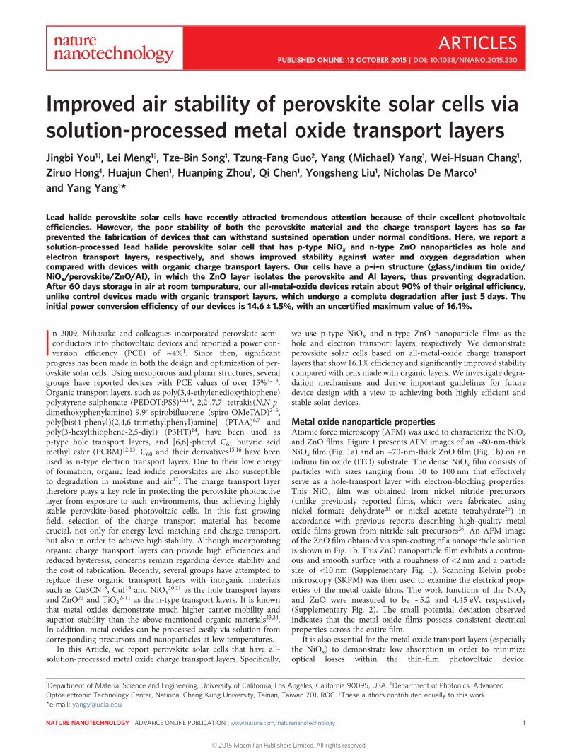
Metal oxide nanoparticle propertiesAtomic force microscopy (AFM) was used to characterize the NiOx
and ZnO films. Figure 1 presents AFM images of an ∼80-nm-thickNiOx film (Fig. 1a) and an ∼70-nm-thick ZnO film (Fig. 1b) on anindium tin oxide (ITO) substrate. The dense NiOx film consists ofparticles with sizes ranging from 50 to 100 nm that effectivelyserve as a hole-transport layer with electron-blocking properties.This NiOx film was obtained from nickel nitride precursors(unlike previously reported films, which were fabricated usingnickel formate dehydrate20 or nickel acetate tetrahydrate25) inaccordance with previous reports describing high-quality metaloxide films grown from nitride salt precursors26. An AFM imageof the ZnO film obtained via spin-coating of a nanoparticle solutionis shown in Fig. 1b. This ZnO nanoparticle film exhibits a continu-ous and smooth surface with a roughness of <2 nm and a particlesize of <10 nm (Supplementary Fig. 1). Scanning Kelvin probemicroscopy (SKPM) was then used to examine the electrical prop-erties of the metal oxide films. The work functions of the NiOx
and ZnO were measured to be ∼5.2 and 4.45 eV, respectively(Supplementary Fig. 2). The small potential deviation observedindicates that the metal oxide films possess consistent electricalproperties across the entire film.
It is also essential for the metal oxide transport layers (especiallythe NiOx) to demonstrate low absorption in order to minimizeoptical losses within the thin-film photovoltaic device.
1Department of Material Science and Engineering, University of California, Los Angeles, California 90095, USA. 2Department of Photonics, AdvancedOptoelectronic Technology Center, National Cheng Kung University, Tainan, Taiwan 701, ROC. †These authors contributed equally to this work.*e-mail: [email protected]
ARTICLESPUBLISHED ONLINE: 12 OCTOBER 2015 | DOI: 10.1038/NNANO.2015.230
NATURE NANOTECHNOLOGY | ADVANCE ONLINE PUBLICATION | www.nature.com/naturenanotechnology 1
© 2015 Macmillan Publishers Limited. All rights reserved
Transmission spectra of the NiOx (80 nm) and ZnO (70 nm) filmsare provided in Supplementary Fig. 3. The NiOx films showrelatively high transmittance in the 300–900 nm range, with theexception of a small portion in the lower visible region that mayresult from defect-related absorption20,25. Similarly, the ZnO filmsshow good transmittance.
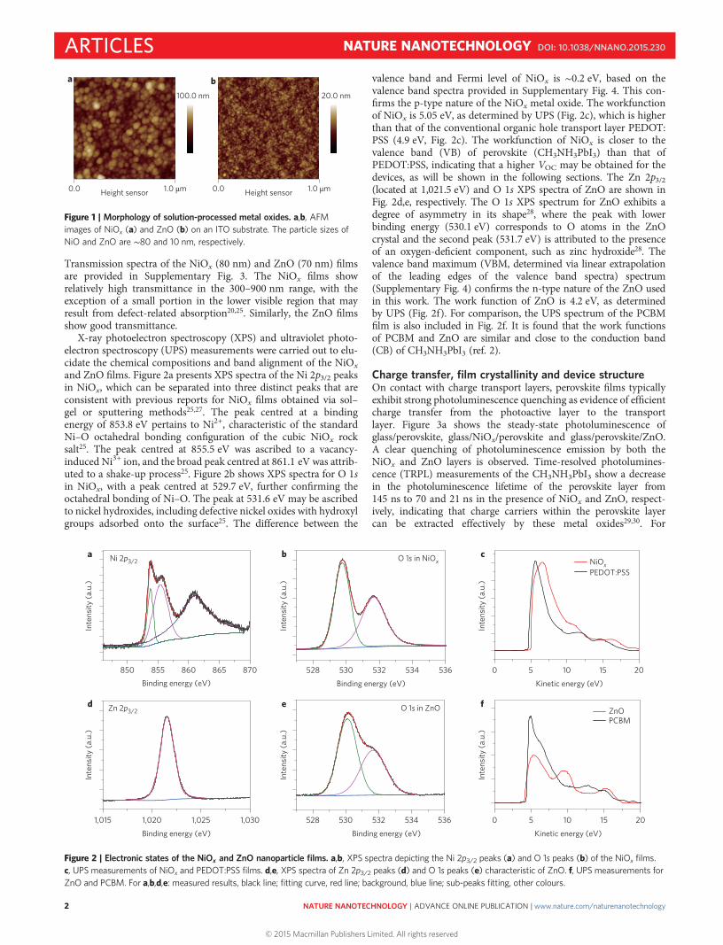
X-ray photoelectron spectroscopy (XPS) and ultraviolet photo-electron spectroscopy (UPS) measurements were carried out to elu-cidate the chemical compositions and band alignment of the NiOx
and ZnO films. Figure 2a presents XPS spectra of the Ni 2p3/2 peaksin NiOx, which can be separated into three distinct peaks that areconsistent with previous reports for NiOx films obtained via sol–gel or sputtering methods25,27. The peak centred at a bindingenergy of 853.8 eV pertains to Ni2+, characteristic of the standardNi–O octahedral bonding configuration of the cubic NiOx rocksalt25. The peak centred at 855.5 eV was ascribed to a vacancy-induced Ni3+ ion, and the broad peak centred at 861.1 eV was attrib-uted to a shake-up process25. Figure 2b shows XPS spectra for O 1sin NiOx, with a peak centred at 529.7 eV, further confirming theoctahedral bonding of Ni–O. The peak at 531.6 eV may be ascribedto nickel hydroxides, including defective nickel oxides with hydroxylgroups adsorbed onto the surface25. The difference between the
valence band and Fermi level of NiOx is ∼0.2 eV, based on thevalence band spectra provided in Supplementary Fig. 4. This con-firms the p-type nature of the NiOx metal oxide. The workfunctionof NiOx is 5.05 eV, as determined by UPS (Fig. 2c), which is higherthan that of the conventional organic hole transport layer PEDOT:PSS (4.9 eV, Fig. 2c). The workfunction of NiOx is closer to thevalence band (VB) of perovskite (CH3NH3PbI3) than that ofPEDOT:PSS, indicating that a higher VOC may be obtained for thedevices, as will be shown in the following sections. The Zn 2p3/2(located at 1,021.5 eV) and O 1s XPS spectra of ZnO are shown inFig. 2d,e, respectively. The O 1s XPS spectrum for ZnO exhibits adegree of asymmetry in its shape28, where the peak with lowerbinding energy (530.1 eV) corresponds to O atoms in the ZnOcrystal and the second peak (531.7 eV) is attributed to the presenceof an oxygen-deficient component, such as zinc hydroxide28. Thevalence band maximum (VBM, determined via linear extrapolationof the leading edges of the valence band spectra) spectrum(Supplementary Fig. 4) confirms the n-type nature of the ZnO usedin this work. The work function of ZnO is 4.2 eV, as determinedby UPS (Fig. 2f). For comparison, the UPS spectrum of the PCBMfilm is also included in Fig. 2f. It is found that the work functionsof PCBM and ZnO are similar and close to the conduction band(CB) of CH3NH3PbI3 (ref. 2).
Charge transfer, film crystallinity and device structureOn contact with charge transport layers, perovskite films typicallyexhibit strong photoluminescence quenching as evidence of efficientcharge transfer from the photoactive layer to the transportlayer. Figure 3a shows the steady-state photoluminescence ofglass/perovskite, glass/NiOx/perovskite and glass/perovskite/ZnO.A clear quenching of photoluminescence emission by both theNiOx and ZnO layers is observed. Time-resolved photolumines-cence (TRPL) measurements of the CH3NH3PbI3 show a decreasein the photoluminescence lifetime of the perovskite layer from145 ns to 70 and 21 ns in the presence of NiOx and ZnO, respect-ively, indicating that charge carriers within the perovskite layercan be extracted effectively by these metal oxides29,30. For
a b
Height sensor0.0 1.0 µm Height sensor0.0
100.0 nm 20.0 nm
1.0 µm
Figure 1 | Morphology of solution-processed metal oxides. a,b, AFMimages of NiOx (a) and ZnO (b) on an ITO substrate. The particle sizes ofNiO and ZnO are ∼80 and 10 nm, respectively.
a c
d e f
b
Inte
nsity
(a.u
.)In
tens
ity (a
.u.)
Inte
nsity
(a.u
.)In
tens
ity (a
.u.)
Inte
nsity
(a.u
.)In
tens
ity (a
.u.)
850
Ni 2p3/2
Zn 2p3/2
O 1s in NiOx
O 1s in ZnO
NiOxPEDOT:PSS
ZnOPCBM
860 870855 865Binding energy (eV)
1,015 1,0301,020 1,025
Binding energy (eV)
528 536532530 534
Binding energy (eV)
0 20105 15
Kinetic energy (eV)
0 20105 15
Kinetic energy (eV)
528 536532530 534
Binding energy (eV)
Figure 2 | Electronic states of the NiOx and ZnO nanoparticle films. a,b, XPS spectra depicting the Ni 2p3/2 peaks (a) and O 1s peaks (b) of the NiOx films.c, UPS measurements of NiOx and PEDOT:PSS films. d,e, XPS spectra of Zn 2p3/2 peaks (d) and O 1s peaks (e) characteristic of ZnO. f, UPS measurements forZnO and PCBM. For a,b,d,e: measured results, black line; fitting curve, red line; background, blue line; sub-peaks fitting, other colours.
ARTICLES NATURE NANOTECHNOLOGY DOI: 10.1038/NNANO.2015.230
NATURE NANOTECHNOLOGY | ADVANCE ONLINE PUBLICATION | www.nature.com/naturenanotechnology2
© 2015 Macmillan Publishers Limited. All rights reserved
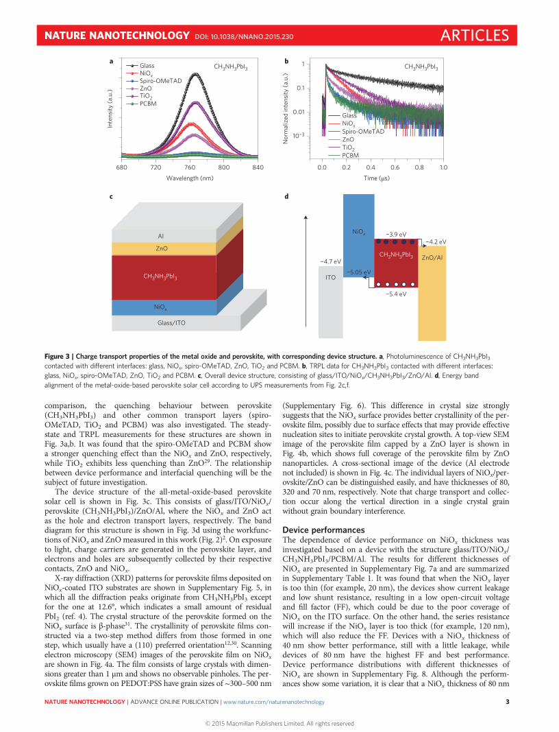
comparison, the quenching behaviour between perovskite(CH3NH3PbI3) and other common transport layers (spiro-OMeTAD, TiO2 and PCBM) was also investigated. The steady-state and TRPL measurements for these structures are shown inFig. 3a,b. It was found that the spiro-OMeTAD and PCBM showa stronger quenching effect than the NiOx and ZnO, respectively,while TiO2 exhibits less quenching than ZnO29. The relationshipbetween device performance and interfacial quenching will be thesubject of future investigation.
The device structure of the all-metal-oxide-based perovskitesolar cell is shown in Fig. 3c. This consists of glass/ITO/NiOx/perovskite (CH3NH3PbI3)/ZnO/Al, where the NiOx and ZnO actas the hole and electron transport layers, respectively. The banddiagram for this structure is shown in Fig. 3d using the workfunc-tions of NiOx and ZnOmeasured in this work (Fig. 2)2. On exposureto light, charge carriers are generated in the perovskite layer, andelectrons and holes are subsequently collected by their respectivecontacts, ZnO and NiOx.
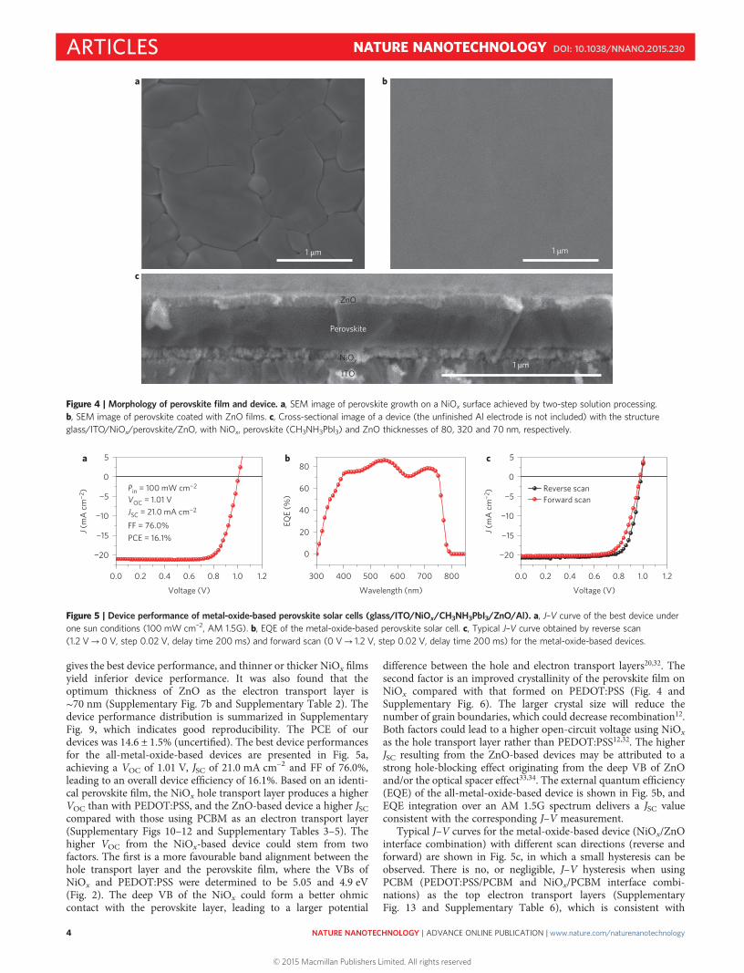
X-ray diffraction (XRD) patterns for perovskite films deposited onNiOx-coated ITO substrates are shown in Supplementary Fig. 5, inwhich all the diffraction peaks originate from CH3NH3PbI3 exceptfor the one at 12.6°, which indicates a small amount of residualPbI2 (ref. 4). The crystal structure of the perovskite formed on theNiOx surface is β-phase31. The crystallinity of perovskite films con-structed via a two-step method differs from those formed in onestep, which usually have a (110) preferred orientation12,30. Scanningelectron microscopy (SEM) images of the perovskite film on NiOx
are shown in Fig. 4a. The film consists of large crystals with dimen-sions greater than 1 μm and shows no observable pinholes. The per-ovskite films grown on PEDOT:PSS have grain sizes of ∼300–500 nm
(Supplementary Fig. 6). This difference in crystal size stronglysuggests that the NiOx surface provides better crystallinity of the per-ovskite film, possibly due to surface effects that may provide effectivenucleation sites to initiate perovskite crystal growth. A top-view SEMimage of the perovskite film capped by a ZnO layer is shown inFig. 4b, which shows full coverage of the perovskite film by ZnOnanoparticles. A cross-sectional image of the device (Al electrodenot included) is shown in Fig. 4c. The individual layers of NiOx/per-ovskite/ZnO can be distinguished easily, and have thicknesses of 80,320 and 70 nm, respectively. Note that charge transport and collec-tion occur along the vertical direction in a single crystal grainwithout grain boundary interference.
Device performancesThe dependence of device performance on NiOx thickness wasinvestigated based on a device with the structure glass/ITO/NiOx/CH3NH3PbI3/PCBM/Al. The results for different thicknesses ofNiOx are presented in Supplementary Fig. 7a and are summarizedin Supplementary Table 1. It was found that when the NiOx layeris too thin (for example, 20 nm), the devices show current leakageand low shunt resistance, resulting in a low open-circuit voltageand fill factor (FF), which could be due to the poor coverage ofNiOx on the ITO surface. On the other hand, the series resistancewill increase if the NiOx layer is too thick (for example, 120 nm),which will also reduce the FF. Devices with a NiOx thickness of40 nm show better performance, still with a little leakage, whiledevices of 80 nm have the highest FF and best performance.Device performance distributions with different thicknesses ofNiOx are shown in Supplementary Fig. 8. Although the perform-ances show some variation, it is clear that a NiOx thickness of 80 nm
a b
c d
Glass/ITO
NiOx
CH3NH3PbI3
ZnO
Al
680 720 760 800 840 0.0
1
0.1
0.01
10−3
1.00.2 0.4 0.6 0.8
Wavelength (nm) Time (µs)
Inte
nsity
(a.u
.)
Nor
mal
ized
inte
nsity
(a.u
.)ITO
NiOx
NiOx
ZnO/AlCH3NH3PbI3
CH3NH3PbI3CH3NH3PbI3
−4.7 eV
Glass
Spiro-OMeTADZnO
PCBMTiO2
NiOx
Glass
Spiro-OMeTADZnO
PCBMTiO2
−5.05 eV
−3.9 eV
−5.4 eV
−4.2 eV
Figure 3 | Charge transport properties of the metal oxide and perovskite, with corresponding device structure. a, Photoluminescence of CH3NH3PbI3contacted with different interfaces: glass, NiOx, spiro-OMeTAD, ZnO, TiO2 and PCBM. b, TRPL data for CH3NH3PbI3 contacted with different interfaces:glass, NiOx, spiro-OMeTAD, ZnO, TiO2 and PCBM. c, Overall device structure, consisting of glass/ITO/NiOx/CH3NH3PbI3/ZnO/Al. d, Energy bandalignment of the metal-oxide-based perovskite solar cell according to UPS measurements from Fig. 2c,f.
NATURE NANOTECHNOLOGY DOI: 10.1038/NNANO.2015.230 ARTICLES
NATURE NANOTECHNOLOGY | ADVANCE ONLINE PUBLICATION | www.nature.com/naturenanotechnology 3
© 2015 Macmillan Publishers Limited. All rights reserved
gives the best device performance, and thinner or thicker NiOx filmsyield inferior device performance. It was also found that theoptimum thickness of ZnO as the electron transport layer is∼70 nm (Supplementary Fig. 7b and Supplementary Table 2). Thedevice performance distribution is summarized in SupplementaryFig. 9, which indicates good reproducibility. The PCE of ourdevices was 14.6 ± 1.5% (uncertified). The best device performancesfor the all-metal-oxide-based devices are presented in Fig. 5a,achieving a VOC of 1.01 V, JSC of 21.0 mA cm–2 and FF of 76.0%,leading to an overall device efficiency of 16.1%. Based on an identi-cal perovskite film, the NiOx hole transport layer produces a higherVOC than with PEDOT:PSS, and the ZnO-based device a higher JSCcompared with those using PCBM as an electron transport layer(Supplementary Figs 10–12 and Supplementary Tables 3–5). Thehigher VOC from the NiOx-based device could stem from twofactors. The first is a more favourable band alignment between thehole transport layer and the perovskite film, where the VBs ofNiOx and PEDOT:PSS were determined to be 5.05 and 4.9 eV(Fig. 2). The deep VB of the NiOx could form a better ohmiccontact with the perovskite layer, leading to a larger potential
difference between the hole and electron transport layers20,32. Thesecond factor is an improved crystallinity of the perovskite film onNiOx compared with that formed on PEDOT:PSS (Fig. 4 andSupplementary Fig. 6). The larger crystal size will reduce thenumber of grain boundaries, which could decrease recombination12.Both factors could lead to a higher open-circuit voltage using NiOx
as the hole transport layer rather than PEDOT:PSS12,32. The higherJSC resulting from the ZnO-based devices may be attributed to astrong hole-blocking effect originating from the deep VB of ZnOand/or the optical spacer effect33,34. The external quantum efficiency(EQE) of the all-metal-oxide-based device is shown in Fig. 5b, andEQE integration over an AM 1.5G spectrum delivers a JSC valueconsistent with the corresponding J–V measurement.
Typical J–V curves for the metal-oxide-based device (NiOx/ZnOinterface combination) with different scan directions (reverse andforward) are shown in Fig. 5c, in which a small hysteresis can beobserved. There is no, or negligible, J–V hysteresis when usingPCBM (PEDOT:PSS/PCBM and NiOx/PCBM interface combi-nations) as the top electron transport layers (SupplementaryFig. 13 and Supplementary Table 6), which is consistent with
a b
c
1 µm 1 µm
1 µm NiOx
Perovskite
ZnO
ITO
Figure 4 | Morphology of perovskite film and device. a, SEM image of perovskite growth on a NiOx surface achieved by two-step solution processing.b, SEM image of perovskite coated with ZnO films. c, Cross-sectional image of a device (the unfinished Al electrode is not included) with the structureglass/ITO/NiOx/perovskite/ZnO, with NiOx, perovskite (CH3NH3PbI3) and ZnO thicknesses of 80, 320 and 70 nm, respectively.
a b c580
Pin = 100 mW cm−2
JSC = 21.0 mA cm−2
FF = 76.0%PCE = 16.1%
VOC = 1.01 V60
40
20
EQE
(%)
0
−5
0
0.0 1.0 1.20.2 0.4 0.6
Voltage (V)
0.8 0.0 1.0 1.20.2 0.4 0.6
Voltage (V)
0.8300 400 500
Wavelength (nm)
600 700 800
J (m
A c
m−2
)
−10
−20
−15
5
Reverse scanForward scan−5
0J (
mA
cm
−2)
−10
−20
−15
Figure 5 | Device performance of metal-oxide-based perovskite solar cells (glass/ITO/NiOx/CH3NH3PbI3/ZnO/Al). a, J–V curve of the best device underone sun conditions (100 mW cm–2, AM 1.5G). b, EQE of the metal-oxide-based perovskite solar cell. c, Typical J–V curve obtained by reverse scan(1.2 V→0 V, step 0.02 V, delay time 200 ms) and forward scan (0 V→ 1.2 V, step 0.02 V, delay time 200 ms) for the metal-oxide-based devices.
ARTICLES NATURE NANOTECHNOLOGY DOI: 10.1038/NNANO.2015.230
NATURE NANOTECHNOLOGY | ADVANCE ONLINE PUBLICATION | www.nature.com/naturenanotechnology4
© 2015 Macmillan Publishers Limited. All rights reserved
previous results12,35. Hysteresis is still a largely controversial issue inperovskite solar cells6,36, but more and more results have recentlysupported the proposal that the hysteresis originates from ionmotion within the perovskite layer35,37–40. When an external fieldis applied, the ions move to the interface between the perovskiteand the charge transport layer, and a temporary dipole forms,which is believed to be the reason for the hysteresis37–40. For aninverted structure, n-type PCBM is deposited on the perovskite,which could penetrate/diffuse into the perovskite layer throughthe pin-holes/grain boundary during processing (spin-coating orannealing35,37). Mobile ions in the perovskite could fully interactwith PCBM to form a PCBM halide radical40, which is thought tostabilize electrostatic properties, reducing the electric field-inducedanion migration that may give rise to hysteresis and thus resultingin no hysteresis35,37–40. It was found that the devices still showobvious hysteresis when the PCBM is used as the bottom electrontransport layer41, which could be explained by the fact that theperovskite and PCBM cannot penetrate into one another, and theion movement in perovskite cannot be fully suppressed40. Inthe case of the metal oxide transport layers, the large metal oxideparticles cannot easily diffuse into the perovskite layer and, moreimportantly, there is no ionic interaction between the perovskiteand the metal oxide, so the ions will remain free to move aroundwith changing bias38, resulting in the observed hysteresis (Fig. 5c).
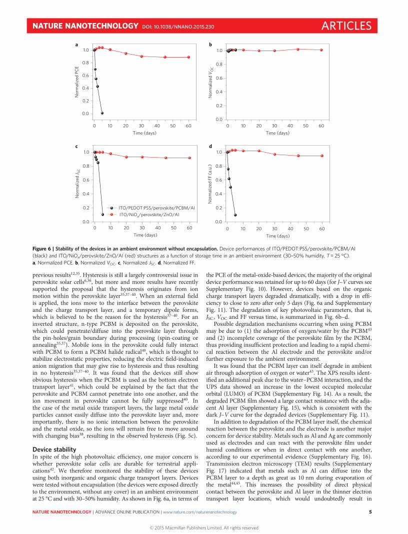
Device stabilityIn spite of the high photovoltaic efficiency, one major concern iswhether perovskite solar cells are durable for terrestrial appli-cations42. We therefore monitored the stability of these devicesusing both inorganic and organic charge transport layers. Deviceswere tested without encapsulation (the devices were exposed directlyto the environment, without any cover) in an ambient environmentat 25 °C and with 30–50% humidity. As shown in Fig. 6a, in terms of
the PCE of the metal-oxide-based devices, the majority of the originaldevice performance was retained for up to 60 days (for J–V curves seeSupplementary Fig. 10). However, devices based on the organiccharge transport layers degraded dramatically, with a drop in effi-ciency to close to zero after only 5 days (Fig. 6a and SupplementaryFig. 11). The degradation of key photovoltaic parameters, that is,JSC, VOC and FF versus time, is summarized in Fig. 6b–d.
Possible degradation mechanisms occurring when using PCBMmay be due to (1) the adsorption of oxygen/water by the PCBM43
and (2) incomplete coverage of the perovskite film by the PCBM,thus providing insufficient protection and leading to a rapid chemi-cal reaction between the Al electrode and the perovskite and/orfurther exposure to the ambient environment.
It was found that the PCBM layer can itself degrade in ambientair through adsorption of oxygen or water43. The XPS results ident-ified an additional peak due to the water–PCBM interaction, and theUPS data showed an increase in the lowest occupied molecularorbital (LUMO) of PCBM (Supplementary Fig. 14). As a result, thedegraded PCBM film showed a large contact resistance with the adja-cent Al layer (Supplementary Fig. 15), which is consistent with thedark J–V curve for the degraded devices (Supplementary Fig. 11).
In addition to degradation of the PCBM layer itself, the chemicalreaction between the perovskite and the electrode is another majorconcern for device stability. Metals such as Al and Ag are commonlyused as electrodes and can react with the perovskite film underhumid conditions or when in direct contact with one another,according to our experimental evidence (Supplementary Fig. 16).Transmission electron microscopy (TEM) results (SupplementaryFig. 17) indicated that metals such as Al can diffuse into thePCBM layer to a depth as great as 10 nm during evaporation ofthe metal44,45. This increases the possibility of direct physicalcontact between the perovskite and Al layer in the thinner electrontransport layer locations, which would undoubtedly result in
a b
c d
1.0
0.8
0.6
0.4
Nor
mal
ized
PC
E
0.2
0.0
1.0
0.8
0.6
0.4
Nor
mal
ized
FF
(a.u
.)0.2
0.0
0 10 20Time (days)
30 40 50 60 0 10 20Time (days)
30 40 50 60
0 10 20
ITO/PEDOT:PSS/perovskite/PCBM/AIITO/NiOx/perovskite/ZnO/AI
Time (days)30 40 50 60 0 10 20
Time (days)30 40 50 60
1.0
0.8
0.6
0.4
Nor
mal
ized
VO
C
0.2
0.0
1.0
0.8
0.6
0.4Nor
mal
ized
J SC
0.2
0.0
Figure 6 | Stability of the devices in an ambient environment without encapsulation. Device performances of ITO/PEDOT:PSS/perovskite/PCBM/Al(black) and ITO/NiOx/perovskite/ZnO/Al (red) structures as a function of storage time in an ambient environment (30–50% humidity, T = 25 °C).a, Normalized PCE. b, Normalized VOC. c, Normalized JSC. d, Normalized FF.
NATURE NANOTECHNOLOGY DOI: 10.1038/NNANO.2015.230 ARTICLES
NATURE NANOTECHNOLOGY | ADVANCE ONLINE PUBLICATION | www.nature.com/naturenanotechnology 5
© 2015 Macmillan Publishers Limited. All rights reserved

decomposition of the perovskite photoactive layer and severe damageto the metal electrode (Supplementary Fig. 18). A thicker PCBM layercould potentially isolate the perovskite from the electrode and par-tially avoid such a chemical reaction (Supplementary Fig. 16).However, this would also result in devices with poor performancesdue to the limited mobility of the PCBM (Supplementary Fig. 19)46.
Through replacement of PCBM with ZnO in an ITO/PEDOT:PSS/perovskite/ZnO/Al device structure, a significant enhancementin stability was achieved (Supplementary Fig. 12). The metal oxideZnO showed good stability in ambient air (SupplementaryFig. 15), and the dense ZnO was able to completely isolate the per-ovskite and Al electrode layers from one another (SupplementaryFig. 16). Finally, the ZnO may serve as a robust diffusion barrier(similar to TiO2) against water due to its scavenging effects47.
Furthermore, we have shown that using metal oxide NiOx as thehole transport layer can further improve the stability when comparedwith devices using PEDOT:PSS (Supplementary Figs 10 and 12).PEDOT:PSS is commonly used as a hole transport layer, but isgenerally considered an unstable transport layer for organicdevices due to its hydrophilic and acidic nature48. The stablep-type metal oxide NiOx was used to overcome this issue andimprove device stability.
ConclusionsIn summary, we have successfully demonstrated efficient perovskitesolar cells employing all-solution-processed metal oxide chargetransport layers. More importantly, it was found that our all-metal-oxide devices show a significant improvement in stability inambient air compared with devices made with organic transportlayers. The mechanism of the improved stability has been discussed.Our results show that metal oxide nanoparticles as transport layersare a promising material with which to construct efficient and stableperovskite solar cells for practical applications.
MethodsMethods and any associated references are available in the onlineversion of the paper.
Received 6 January 2015; accepted 3 September 2015;published online 12 October 2015
References1. Kojima, A., Teshima, K., Shirai, Y. & Miyasaka, T. Organometal halide
perovskites as visible-light sensitizers for photovoltaic cells. J. Am. Chem. Soc.131, 6050–6051 (2009).
2. Kim, H. S. et al. Lead iodide perovskite sensitized all-solid-state submicronthin film mesoscopic solar cell with efficiency exceeding 9%. Sci. Rep. 2,591 (2012).
3. Lee, M. M. et al. Efficient hybrid solar cells based on meso-superstructuredorganometal halide perovskites. Science 338, 643–647 (2012).
4. Burschka, J. et al. Sequential deposition as a route to high-performanceperovskite-sensitized solar cells. Nature 499, 316–319 (2013).
5. Liu, M., Johnston, M. B. & Snaith, H. J. Efficient planar heterojunctionperovskite solar cells by vapour deposition. Nature 501, 395–398 (2013).
6. Jeon, N. J. et al. Solvent engineering for high-performance inorganic–organichybrid perovskite solar cells. Nature Mater. 13, 897–903 (2014).
7. Yang, W. S. et al. High-performance photovoltaic perovskite layers fabricatedthrough intramolecular exchange. Science 348, 1234–1237 (2015).
8. Im, J. H., Jang, I. H., Pellet, N., Grätzel, M. & Park, N. G. Growth ofCH3NH3PbI3 cuboids with controlled size for high-efficiency perovskite solarcells. Nature Nanotech. 9, 927–932 (2014).
9. Zhou, H. et al. Interface engineering of highly efficient perovskite solar cells.Science 345, 542–546 (2014).
10. Wojciechowski, K. et al. Heterojunction modification for highlyefficient organic–inorganic perovskite solar cells. ACS Nano 8,12701–12709 (2014).
11. Xiao, M. et al. A fast deposition–crystallization procedure for highly efficientlead iodide perovskite thin-film solar cells. Angew. Chem. Int. Ed. 53,9898–9903 (2014).
12. You, J. et al. Moisture assisted perovskite film growth for high performance solarcells. Appl. Phys. Lett. 105, 183902 (2014).
13. Xiao, Z. G. et al. Efficient, high yield perovskite photovoltaic devices grown byinterdiffusion of solution-processed precursor stacking layers. Energy Environ.Sci. 7, 2619–2623 (2014).
14. Conings, B. et al. Perovskite-based hybrid solar cells exceeding 10% efficiencywith high reproducibility using a thin film sandwich approach. Adv. Mater. 26,2041–2046 (2014).
15. Jeng, J. Y. et al. CH3NH3PbI3 perovskite/fullerene planar-heterojunction hybridsolar cells. Adv. Mater. 25, 3727–3732 (2013).
16. Liang, P. W. et al. Additive enhanced crystallization of solution-processedperovskite for highly efficient planar-heterojunction solar cells. Adv. Mater. 26,3748–3754 (2014).
17. Noh, J. H. et al. Chemical management for colorful, efficient, and stable inorganic–organic hybrid nanostructured solar cells. Nano Lett. 13, 1764–1769 (2013).
18. Qin, P. et al. Inorganic hole conductor-based lead halide perovskite solar cellswith 12.4% conversion efficiency. Nature Commun. 5, 3834 (2014).
19. Christians, J. A. et al. An inorganic hole conductor for organo-lead halideperovskite solar cells improved hole conductivity with copper iodide. J. Am.Chem. Soc. 136, 758–764 (2014).
20. Jeng, J. Y. et al. Nickel oxide electrode interlayer in CH3NH3PbI3 perovskite/PCBM planar-heterojunction hybrid solar cells. Adv. Mater. 26,4107–4113 (2014).
21. Zhu, Z. L. et al. High-performance hole-extraction layer of sol–gel-processedNiOx nanocrystals for inverted planar perovskite solar cells. Angew. Chem. Int.Ed. 53, 12571–12575 (2014).
22. Liu, D. Y. & Kelly, T. L. Perovskite solar cells with a planar heterojunctionstructure prepared using room-temperature solution processing techniques.Nature Photon. 8, 133–138 (2014).
23. Hau, S. K. et al. Air-stable inverted flexible polymer solar cells using zinc oxidenanoparticles as an electron selective layer. Appl. Phys. Lett. 92, 253301 (2008).
24. Qian, L. et al. Stable and efficient quantum-dot light-emitting diodes based onsolution-processed multilayer structures. Nature Photon. 5, 543–548 (2011).
25. Manders, J. R. et al. Solution-processed nickel oxide hole transport layers in highefficiency polymer photovoltaic cells. Adv. Funct. Mater. 23, 2993–3001 (2013).
26. Rim, Y. S. et al. Direct light pattern integration of low-temperature solution-processed all-oxide flexible electronics. ACS Nano 8, 9680–9686 (2014).
27. Wang, K. C. et al. Low-temperature sputtered nickel oxide compact thin film aseffective electron blocking layer for mesoscopic NiOx/CH3NH3PbI3 perovskiteheterojunction solar cells. ACS Appl. Mater. Interfaces 6, 11851–11858 (2014).
28. Sun, Y. M. et al. Inverted polymer solar cells integrated with a low-temperature-annealed sol-gel-derived ZnO film as an electron transport layer. Adv.Mater. 23, 1679–1683 (2011).
29. Docampo, P. et al. Efficient organometal trihalide perovskite planar-heterojunction solar cells on flexible polymer substrates. Nature Commun. 4,2761 (2013).
30. You, J. et al. Low-temperature solution-processed perovskite solar cells with highefficiency and flexibility. ACS Nano 8, 1674–1680 (2014).
31. Stoumpos, C. C. et al. Semiconducting tin and lead iodide perovskites withorganic cations: phase transitions, high mobilities, and near-infraredphotoluminescent properties. Inorg. Chem. 52, 9019–9038 (2013).
32. Park, J. H. et al. Efficient CH3NH3PbI3 perovskite solar cells employingnanostructured p-type NiO electrode formed by a pulsed laser deposition. Adv.Mater. 27, 4013–4019 (2015).
33. You, J. et al. Electroluminescence behavior of ZnO/Si heterojunctions: energyband alignment and interfacial microstructure. J. Appl. Phys. 107, 083701 (2010).
34. Gilot, J. et al. The use of ZnO as optical spacer in polymer solar cells: theoreticaland experimental study. Appl. Phys. Lett. 91, 113520 (2007).
35. Shao, Y. C., Xiao, Z. G., Bi, C., Yuan, Y. B. & Huang, J. S. Origin and eliminationof photocurrent hysteresis by fullerene passivation in CH3NH3PbI3 planarheterojunction solar cells. Nature Commun. 5, 5784 (2014).
36. Snaith, H. J. et al. Anomalous hysteresis in perovskite solar cells. J. Phys. Chem.Lett. 5, 1511–1515 (2014).
37. Stranks, S. D. & Sanith, H. J. Metal-halide perovskites for photovoltaic and light-emitting devices. Nature Nanotech. 10, 391–402 (2015).
38. Bastiani, M. D., Binda, M., Gandini, M., Ball, J. & Petrozza, A. Charge extractionlayer investigation for high efficiency and hysteresis-less organo lead halideperovskite solar cell. Proc. MRS Spring Meeting C4.04 (2015).
39. Zhang, Y. et al. Charge selective contacts, mobile ions and anomalous hysteresisin organic–inorganic perovskite solar cell. Mater. Horiz. 2, 315–322 (2015).
40. Xu, J. X. et al. Perovskite–fullerene hybrid materials suppress hysteresis in planardiodes. Nature Commun. 6, 7081 (2015).
41. Ryu, S. et al. Fabrication of metal-oxide-free CH3NH3PbI3 perovskite solar cellsprocessed at low temperature. J. Mater. Chem. A 3, 3271–3275 (2015).
42. Mei, A. et al. A hole-conductor-free, fully printable mesoscopic perovskite solarcell with high stability. Science 345, 295–298 (2014).
43. Bao, Q. et al. Oxygen- and water-based degradation in [6,6]-phenyl-C61-butyricacid methyl ester (PCBM) films. Adv. Energy Mater. 4, 1301272 (2014).
44. Peumans, P. et al. Small molecular weight organic thin-film photodetectors andsolar cells. J. Appl. Phys. 93, 3693–3722 (2003).
ARTICLES NATURE NANOTECHNOLOGY DOI: 10.1038/NNANO.2015.230
NATURE NANOTECHNOLOGY | ADVANCE ONLINE PUBLICATION | www.nature.com/naturenanotechnology6
© 2015 Macmillan Publishers Limited. All rights reserved

45. Durr, A. C. et al. Morphology and thermal stability of metal contacts oncrystalline organic films. Adv. Mater. 14, 961–963 (2002).
46. Seo, J. et al. Benefits of very thin PCBM and LiF layers for solution-processedp–i–n perovskite solar cells. Energy Environ. Sci. 7, 2642–2646 (2014).
47. Lee, K. H. et al. Air-stable polymer electronic devices. Adv. Mater. 19,2445–2449 (2007).
48. De Jong, M. P. et al. Stability of the interface between indium-tin-oxide and poly(3,4-ethylenedioxythiophene)/poly(styrenesulfonate) in polymer light-emittingdiodes. Appl. Phys. Lett. 77, 2255–2257 (2000).
AcknowledgementsThis work was supported financially by a grant from the National Science Foundation(ECCS-1202231) and the Air Force Office of Scientific Research (FA9550-12-1-0074).T.F.G. acknowledges financial support from the Ministry of Science and Technology(MOST), Taiwan ROC (MOST 103-2119-M-006-020 andMOST 102-2628-M-006-001-MY3).The authors thank E. Zhu and Y. Li for TEM measurement, S. Adam for help with SKPM
measurements and Y.S. Rim for discussions regarding NiOx synthesis. The authorsalso thank G. Li for discussions and E. Young for proof reading.
Author contributionsJ.Y. and Y.Y. designed the experiments. J.Y. and L.M. performed device fabrication and dataanalysis. T.Z.S., H.C., Y.(M.)Y., W.H.C., H.Z., Q.C., Y.S.L. and N.D.M. contributedmaterials/analysis tools. T.F.G. commented on the project. J.Y., L.M. and Y.Y. co-wrote thepaper. All authors discussed the results and commented on the manuscript.
Additional informationSupplementary information is available in the online version of the paper. Reprints andpermissions information is available online at www.nature.com/reprints. Correspondence andrequests for materials should be addressed to Y.Y.
Competing financial interestsThe authors declare no competing financial interests.
NATURE NANOTECHNOLOGY DOI: 10.1038/NNANO.2015.230 ARTICLES
NATURE NANOTECHNOLOGY | ADVANCE ONLINE PUBLICATION | www.nature.com/naturenanotechnology 7
© 2015 Macmillan Publishers Limited. All rights reserved

MethodsNiOx precursor solution. Nickel(II) nitrate hexahydrate (Ni(NO3)2·6H2O) (SigmaAldrich) was dissolved in ethylene glycol solution containing 1 M nickel(II) nitratehexahydrate with ethylenediamine (Aldrich). The solution was spin-cast onto glass/ITO substrate at a spin speed ranging from 1,000 to 4,000 r.p.m. for 90 s to controlthe NiOx thickness. The substrate was then post-annealed at 300 °C in ambient airfor 60 min.
ZnO nanoparticles synthesis. The chemical synthesis of ZnO nanoparticles wasperformed using the method outlined in our previous publication49, but methanolwas totally removed to prevent the residual solvent decomposing the perovskitelayer, as it has been confirmed that some solvents, such as ethanol and methanol, candegrade/decompose perovskite. After drying the ZnO nanoparticles, the powder wasthen redispersed in chlorobenzene to a concentration of 2%. The thicknesses of theZnO layer were controlled by the spin speed.
Device fabrication and measurement. PEDOT:PSS was spin-cast onto the ITOsurface at 4,000 r.p.m. and then annealed at 120 °C for 15 min in ambient air. TheNiOx precursor was spin-coated on the ITO and annealed at 300 °C for 60 min inambient air. The substrates were then transferred into a nitrogen glove box forcoating of the perovskite layer, where a two-step spin-coating process was adopted.(It was found that a one-step solution process cannot form a high quality ofperovskite film on the NiOx
20,21, possibly due to the surface roughness of the NiOx
inducing fast crystallization in the perovskite, so the two-step process was adoptedhere to obtain a sufficiently high quality perovskite layer35.) The PbI2 layer was spin-coated first using a 460 mg ml–1 solution and dried at 70 °C for 10min, then 50 mg ml–1
of CH3NH3I solution was coated onto the PbI2 layer, after which the film was takenout for annealing in ambient air at 100 °C for 2 h. For PCBM coating, a 2% PCBM inchlorobenzene solution was coated onto the perovskite layer. For the ZnO layer,different thicknesses of ZnO were coated onto the perovskite surface by controllingthe spin speed. Finally, the device was transferred to a vacuum chamber for Alelectrode evaporation. The device area was 0.1 cm2. J–V characteristics of thephotovoltaic cells were measured using a Keithley 2400 source unit under asimulated AM 1.5G spectrum. With an Oriel 9600 solar simulator, the light intensitywas calibrated by a KG-5 Si diode. I–Vmeasurements were carried out in a nitrogenglove box. The devices were measured in reverse scan (1.2 V→ 0 V, step 0.02 V,delay time 200 ms) and forward scan (0 V→ 1.2 V, step 0.02 V, delay time 200 ms).The differences between reverse and forward scans are shown in Fig. 5c,Supplementary Fig. 13 and Supplementary Table 6). The devices were taken out forEQE measurements using an Enli tech (Taiwan) EQE measurement system.
SKPM. SKPM was performed on perovskite samples under ambient conditionsusing a Dimension Icon scanning probe microscope (Bruker Nano) in single-passfrequency-modulated (FM) mode. FM detection maximizes the spatial resolution bymeasuring the local electrostatic force gradient present solely at the apex of the AFMtip, thereby reducing the contributions of the tip cone and cantilever that are presentin the more common amplitude-modulated detection schemes. Application of anoff-resonant a.c. voltage (∼5 V, 2 kHz) between a conductive AFM probe (heavily
doped Si tips, Bruker) and the grounded sample alters the effective spring constantof the cantilever and thus modulates its resonant frequency due to an inducedelectric force gradient. Spatial variations in the surface potential/workfunction weredirectly measured by nulling the local electrostatic force gradient arising fromcontact potential differences between the AFM tip and the film surface by using abias-controlled feedback loop. A minimum force set-point was applied, as indicatedby nominal phase contrast, to reduce potential artefacts in the surface potentialimages. The workfunction of the Si tip (heavily doped Si tips) was calibratedusing a freshly cleaved highly ordered pyrolytic graphite (HOPG) substrate ofknown workfunction (4.6 eV), and the workfunction of the Si tip used was foundto be 4.4 eV.
TEM. High-resolution TEM images and energy-dispersive X-ray spectroscopy(EDS) data were obtained on an FEI TITAN transmission electron microscopeoperated at 300 kV. The sample glass/ITO/PCBM (30 nm)/Al (30 nm) was used forthe TEM sample. The focused ion beam technique was used for cross-TEMsample preparation.
XRD. XRD patterns (θ–2θ scans) were obtained from samples of perovskitedeposited on substrates using a double-axis X-ray diffractometer (Bede D1)equipped with a focusing graded X-ray mirror with monochromatic CuKα(λ = 1.5405 Å) radiation source. Scans were taken with a 0.5-mm-wide source anddetector slits, and with X-ray generator settings of 40 kV and 30 mA.
SEM. A field-emission scanning electron microscope (FEI Nova 230 NanoSEM) wasused to acquire SEM images. The instrument used an electron beam accelerated at500 V to 30 kV, enabling operation at a variety of currents.
Steady photoluminescence and TRPL. Steady-state photoluminescence wasmeasured using a Horiba Jobinyvon system with excitation at 600 nm. In the TRPLmeasurement, the samples were excited by a pulsed laser (PDL 800-B system with anexternal trigger), with a wavelength and frequency of 632 nm and 1 MHz,respectively. The photoluminescence photons were counted by a Picoharp 300 afterbeing pre-amplified by a pre-amplifier module (PAM102, PicoQuant).
XPS and UPS. XPS measurements were carried out on an XPS AXIS Ultra DLD(Kratos Analytical). An Al Kα (1,486.6 eV) X-ray was used as the excitation source.UPS measurements were carried out to determine the work function of thematerials, and a He discharge lamp, emitting ultraviolet energy at 21.2 eV, was usedfor excitation. All UPS measurements of the onset of photoemission to determinethe workfunction were performed using standard procedures with a −9 V biasapplied to the samples.
References49. You, J. et al. Metal oxide nanoparticles as electron transport layer in high
performance and stable inverted polymer solar cells. Adv. Mater. 24,5267–5272 (2012).
ARTICLES NATURE NANOTECHNOLOGY DOI: 10.1038/NNANO.2015.230
NATURE NANOTECHNOLOGY | www.nature.com/naturenanotechnology
© 2015 Macmillan Publishers Limited. All rights reserved