Imprinting localized plasmons for enhanced solar...
6
Imprinting localized plasmons for enhanced solar cells This article has been downloaded from IOPscience. Please scroll down to see the full text article. 2012 Nanotechnology 23 385202 (http://iopscience.iop.org/0957-4484/23/38/385202) Download details: IP Address: 150.203.45.59 The article was downloaded on 05/10/2012 at 02:39 Please note that terms and conditions apply. View the table of contents for this issue, or go to the journal homepage for more Home Search Collections Journals About Contact us My IOPscience
Transcript of Imprinting localized plasmons for enhanced solar...

Imprinting localized plasmons for enhanced solar cells
This article has been downloaded from IOPscience. Please scroll down to see the full text article.
2012 Nanotechnology 23 385202
(http://iopscience.iop.org/0957-4484/23/38/385202)
Download details:
IP Address: 150.203.45.59
The article was downloaded on 05/10/2012 at 02:39
Please note that terms and conditions apply.
View the table of contents for this issue, or go to the journal homepage for more
Home Search Collections Journals About Contact us My IOPscience
IOP PUBLISHING NANOTECHNOLOGY
Nanotechnology 23 (2012) 385202 (5pp) doi:10.1088/0957-4484/23/38/385202
Imprinting localized plasmons forenhanced solar cellsRicky B Dunbar1, Thomas Pfadler1,2, Niraj N Lal3, Jeremy J Baumberg3
and Lukas Schmidt-Mende2
1 Department of Physics and Center for NanoScience (CeNS), Ludwig-Maximilians University (LMU)Munich, Amalienstraße 54, 80799 Munich, Germany2 Department of Physics, University of Konstanz, Universitatsstraße 10, 78457 Konstanz, Germany3 NanoPhotonics Centre, Cavendish Laboratory, University of Cambridge, CB3 0HE, UK
E-mail: [email protected]
Received 23 April 2012, in final form 26 July 2012Published 4 September 2012Online at stacks.iop.org/Nano/23/385202
AbstractImprinted silver nanovoid arrays are investigated via angle-resolved reflectometry todemonstrate their suitability for plasmonic light trapping. Both wavelength- andsubwavelength-scale nanovoids are imprinted into standard solar cell architectures to achievenanostructured metallic electrodes which provide enhanced absorption for improving solarcell performance. The technique is versatile, low-cost and scalable and can be applied to awide range of organic semiconductors. Absorption features which are independent of incidentpolarization and weakly dependent on incident angle reveal localized plasmonic modes at thestructured interface. Metallic nanostructure–PCPDTBT:PCBM samples demonstrateabsorption enhancements of up to 40%. The structured interface provides light trapping, whichboosts absorption at wavelengths where the semiconductors absorb poorly.
S Online supplementary data available from stacks.iop.org/Nano/23/385202/mmedia
(Some figures may appear in colour only in the online journal)
1. Introduction
The field of plasmonics has advanced tremendously inrecent years [1, 2], largely enabled by significant advancesin nanofabrication technology. Total light absorption hasbeen theoretically as well as experimentally investigated forperiodic nanostructured metal surfaces [3, 4]. Teperik et al [5]shows omnidirectional absorption of light for close-packedmetallic nanovoids. Solar cells stand to benefit greatly fromplasmonic light trapping, where plasmonic excitation leads toan increased absorption of light in the adjacent semiconductorfilm and a consequent enhancement in charge-carriergeneration (or, in the case of organic semiconductors, excitongeneration) [6–10]. Previous reports have demonstrated thatmetallic nanovoid arrays are capable of hosting localizedas well as propagating plasmonic excitations and aretherefore extremely interesting for incorporation into solarcells in the form of nanostructured electrodes [11–13].Here we investigate metallic nanovoid arrays fabricated
using a simple, scalable, low-cost nanoimprint techniqueand assess their potential for trapping incident light inadjacent films. We first address plasmonic excitation onimprinted transparent dielectric–silver nanovoid interfaces.These excitations can decay radiatively via out-couplingto photons or non-radiatively via absorption in the silverfilm. In order to address the suitability of this method formanufacturing highly absorbing solar cells, we then fabricatesamples with organic semiconductor (OSC)–silver nanovoidinterfaces. We thereby gain an insight into the effect ofabsorption in the OSC on plasmonic modes at the interface. Insamples with absorbing dielectric–silver interfaces, plasmonicexcitations have two non-radiative decay channels: absorptionin the silver and in the OSC film. Decay via absorption inthe OSC film is desirable for solar cells, as this absorbedenergy can be converted into electrical current. In contrast,absorption in the silver is a loss mechanism. An efficienttransfer of trapped mode energy to absorption in the adjacentOSC film is a requirement for obtaining a significantabsorption and hence efficiency enhancement in organic solar
10957-4484/12/385202+05$33.00 c© 2012 IOP Publishing Ltd Printed in the UK & the USA
Nanotechnology 23 (2012) 385202 R B Dunbar et al
cells with structured metallic electrodes. Previous reportsof organic–silver systems indicate that energy stored inpure SPP modes [6], localized nanovoid modes [14], andnear-field/far-field modes at metallic nanoparticles [15] isindeed efficiently transferred to an adjacent organic film (withan efficiency as high as 95% [6]).
2. Materials and methods
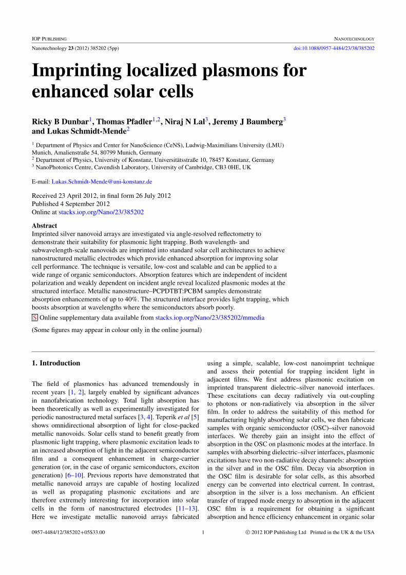
To elucidate the nature of the plasmonic excitation onimprinted nanovoids we first imprint silver nanovoid arraysadjacent to an optically transparent dielectric, PMMA(polymethylmethacrylate). The real part of the refractiveindex varies between 1.2 and 1.5 in the investigated photonenergy range and the imaginary part is negligible [16].PMMA films of thickness around 300 nm are obtainedby spin-coating from a toluene solution (96.9 mg ml−1)for 1 min at 3000 rpm onto 2 cm2 substrates. Quartzsubstrates are used for spectroscopy measurements and quartzsubstrates coated with indium tin oxide are used for SEMimaging to minimize charging during imaging. Nanoimprintlithography [14, 17–19] (450 bar, 100 ◦C, 5 min) isthen used to structure the surface of the polymer film.The periodicity of the structured film is equal to thatof the stamps, and the feature diameter and heightare determined by the imprinting temperature, pres-sure and duration. Chips of anodized aluminum oxide(AAO) [20, 21] that feature large-area hexagonal lattices ofpores are used as stamps. The nanostructured polymer filmsobtained (figures 1(a)–(d), where (a) and (c) show PMMAfilms and (b) and (d) show OSC films) are then covered witha layer of silver (nominally 150 nm thick) via evaporation.This silver layer conforms to the topography of the underlyingpolymer film to produce samples with a metallic nanovoidarray interface (figure 1(e)) [14]. Flat reference samples arefabricated in parallel under identical conditions without theimprinting step.
To investigate imprinted nanovoid light trapping insolar cell geometries, we fabricate additional sampleswith organic semiconductor (OSC)–silver nanovoid inter-faces. Here we use an OSC film of poly[2,6-(4,4-bis-(2-ethylhexyl)-4H-cyclopenta[2,1-b;3,4-b′]dithiophene)-alt-4,7-(2,1,3-benzothiadiazole)]:phenyl-C61-butyric acid methylester (PCPDTBT:PCBM), two components commonly usedin organic photovoltaics [22]. Precursor concentrations of22.2 (PCPDTBT) and 24 mg ml−1 (PCBM) in chlorobenzene(mixed 1:2), and spin-coating conditions (1500 rpm for 1 min)are chosen to obtain films of 100 nm thickness, consistent withoptimized solar cells of this type [22].
Stamps with two pore periodicities (490 and 95 nm) areused to fabricate nanovoid arrays of different pitches, whichwe refer to as wavelength-scale and subwavelength-scalevoids respectively. The voids for the dielectric sample (figures1(a) and (c)) can be well approximated by an array ofhemispheres with characteristic void diameters of 470 and60 nm respectively. The pore depths are 195 and 25 nmrespectively (figure 1(f)).
Figure 1. (a)–(d) SEM images of imprinted nanostructures. A layerof indium tin oxide is visible between the structured polymer andthe glass substrate in cross-section images ((a), (b)). (a) Transparentdielectric and (b) organic semiconductor wavelength-scalestructures (490 nm period) and (c) top view of (a). (d) Top view oforganic semiconductor subwavelength-scale structure (95 nmperiod). (e) Sample and measurement geometry. (f) Scale diagramof wavelength-scale and subwavelength-scale voids (transparentdielectric). Additional SEM pictures are shown in the supplementaryinformation (available at stacks.iop.org/Nano/23/385202/mmedia).
Nanoimprint lithography is performed under identicalconditions with the same stamps for the semiconductingcomposite to fabricate samples that are directly comparablewith the transparent dielectric samples. Due to the reducedthickness of the OSC layer (necessary for efficient charge-carrier extraction in solar cells), the voids imprinted withthe wavelength-scale stamp have a truncated hemisphericalshape (figure 1(b)) and hence a smaller depth (115 nm) thanthe voids in the dielectric sample (195 nm). Otherwise, thedielectric and OSC samples have equal void period, diameterand depth (see also figure SI.1 available at stacks.iop.org/Nano/23/385202/mmedia).
Specular reflectance spectra (figure 1(e)) are measuredfrom 1.4 to 2.9 eV with a supercontinuum white-light lasersource (Fianium SC-450-6) for incidence angles 0◦–45◦.The incident beam is passed through a polarizer to obtaineither TM- or TE-polarized light. The reflected beam isfiber-collected, separated into visible and IR wavelengths viabeam-splitters and detected using Ocean Optics QE65000and NIRQuest spectrometers respectively [11]. ReflectanceR is normalized to a flat silver mirror and absorption A isobtained via A = 1 − R. Non-specular reflection is measuredto be negligible—indicating that light which would otherwisebe out-coupled from the sample as non-specular reflectionis preferentially trapped within the sample via couplingto surface modes [11] and or multiple internal reflections.Similar reflectance spectra are measured over the entire areaof each sample.
2

Nanotechnology 23 (2012) 385202 R B Dunbar et al
Figure 2. First row, transparent dielectric (PMMA)–Ag, and second row, organic semiconductor (PCPDTBT:PCBM)–Ag nanovoidinterfaces. Absorption spectra are plotted with a logarithmic (base 10) color scale for incidence angles 0◦–45◦. The incident polarization andsample geometries are indicated for each column. Flat references are shown in the supplementary information (figure S1.2 available atstacks.iop.org/Nano/23/385202/mmedia). Prominent absorption features in (a) and (b) are marked with dashed lines.
3. Results and discussion
Absorption in the structured dielectric–Ag samples (figures2(a)–(d)) occurs exclusively in the silver layer as the adjacentdielectric layer absorbs negligibly in this photon energyregion. For the wavelength-scale voids, a number of broadabsorption features can be seen between 1.9 and 2.9 eV(indicated by the black dashed line in figures 2(a) and (b)),consistent with plasmonic excitation at the nanostructureddielectric–Ag interface. The excitation of these absorptionfeatures is strongest for incident angles between 10◦ and45◦; however, other than this, no strong angle dependenceis observed. The similarity between the absorption spectrafor TE and TM polarizations indicates that these modesare localized surface plasmons (LSPs), which unlike surfaceplasmon polaritons (SPPs) are polarization independent forhemispherical nanovoids [2, 11]. This is in qualitativeagreement with measured and simulated spectra obtainedfor similar nanovoid arrays reported elsewhere [11, 13, 23].Dispersive energy minibands (most prominent in figure 2(b))indicate coupling between localized plasmons in neighboringvoids [24]. The absence of well defined, strongly dispersiveTM absorption features, a signature of SPP excitation,indicates that SPP excitation is inhibited by the limitedlarger-scale order of the nanovoid array (figures 1(a) and (c)).
An absorption feature for the transparent dielectricsubwavelength-scale void sample appears at the upper energylimit of the measurement range (2.9 eV) (figures 2(c) and (d)).This feature is present for both TM and TE incident light,indicating that, like the wavelength-scale void sample, it isdue to an LSP mode. This resonance is at the high-energy edgeof the visible light region; no evidence of mode excitation isobserved for the majority of the visible light and infra-redregions. The higher absorption of the transparent dielectric
wavelength-scale sample (figures 2(a) and (b)) highlights thepromise of LSPs with resonances within the visible photonenergy range for optoelectronic applications.
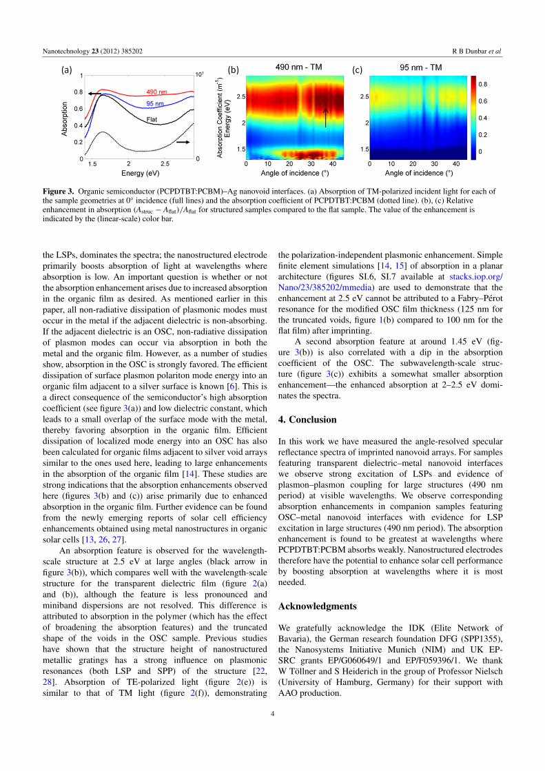
We then compare these results with our imprintednanovoid light trapping geometries, using a PCPDTBT:PCBMmatrix with silver nanovoid interfaces (figures 2(e)–(h)).The real part of the composite refractive index of thePCPDTBT:PCBM material varies between 1.8 and 2 in themeasured optical range and the absorption coefficient featuresa prominent dip between 2 and 2.5 eV (figure 3(a)) [25].
The limited semiconductor absorption in the range2–2.5 eV and below 1.5 eV is evident in the absorption spectrafor the flat architecture (figures 3(a) and SI.2(c), (d) availableat stacks.iop.org/Nano/23/385202/mmedia). We see that theabsorption of the structured electrodes is significantly larger(figures 3(a) and 2(e)–(h)), especially in the 2–2.5 eV region.Similar to the transparent dielectric subwavelength-scalestructure, an absorption enhancement feature is measured atthe upper energy limit of the measurement range around2.9 eV (figures 3(a), 2(g) and (h)). No strong dependence onincident polarization is observed.
Wavelength-scale voids exhibit stronger light trappingthan their subwavelength counterparts (figures 2((e)–(h))and 3), consistent with the transparent dielectric samples(figures 2(a)–(d)). At 0◦ incidence we observe total absorptionenhancements (integrated over the energy range between2.9 and 1.4 eV (430 and 880 nm)) of 40% and 20% forthe wavelength- and subwavelength-scale voids respectively(figure 3(a)). Spectra of relative absorption enhancement((Astruc−Aflat)/Aflat) do not display a strong angle dependence(figures 3(b) and (c))—the enhancement primarily occursat energies where the OSC absorbs poorly (compare theabsorption coefficient, figure 3(a)). In other words, thedispersive nature of the organic semiconductor, and not of
3
Nanotechnology 23 (2012) 385202 R B Dunbar et al
Figure 3. Organic semiconductor (PCPDTBT:PCBM)–Ag nanovoid interfaces. (a) Absorption of TM-polarized incident light for each ofthe sample geometries at 0◦ incidence (full lines) and the absorption coefficient of PCPDTBT:PCBM (dotted line). (b), (c) Relativeenhancement in absorption (Astruc − Aflat)/Aflat for structured samples compared to the flat sample. The value of the enhancement isindicated by the (linear-scale) color bar.
the LSPs, dominates the spectra; the nanostructured electrodeprimarily boosts absorption of light at wavelengths whereabsorption is low. An important question is whether or notthe absorption enhancement arises due to increased absorptionin the organic film as desired. As mentioned earlier in thispaper, all non-radiative dissipation of plasmonic modes mustoccur in the metal if the adjacent dielectric is non-absorbing.If the adjacent dielectric is an OSC, non-radiative dissipationof plasmon modes can occur via absorption in both themetal and the organic film. However, as a number of studiesshow, absorption in the OSC is strongly favored. The efficientdissipation of surface plasmon polariton mode energy into anorganic film adjacent to a silver surface is known [6]. This isa direct consequence of the semiconductor’s high absorptioncoefficient (see figure 3(a)) and low dielectric constant, whichleads to a small overlap of the surface mode with the metal,thereby favoring absorption in the organic film. Efficientdissipation of localized mode energy into an OSC has alsobeen calculated for organic films adjacent to silver void arrayssimilar to the ones used here, leading to large enhancementsin the absorption of the organic film [14]. These studies arestrong indications that the absorption enhancements observedhere (figures 3(b) and (c)) arise primarily due to enhancedabsorption in the organic film. Further evidence can be foundfrom the newly emerging reports of solar cell efficiencyenhancements obtained using metal nanostructures in organicsolar cells [13, 26, 27].
An absorption feature is observed for the wavelength-scale structure at 2.5 eV at large angles (black arrow infigure 3(b)), which compares well with the wavelength-scalestructure for the transparent dielectric film (figure 2(a)and (b)), although the feature is less pronounced andminiband dispersions are not resolved. This difference isattributed to absorption in the polymer (which has the effectof broadening the absorption features) and the truncatedshape of the voids in the OSC sample. Previous studieshave shown that the structure height of nanostructuredmetallic gratings has a strong influence on plasmonicresonances (both LSP and SPP) of the structure [22,28]. Absorption of TE-polarized light (figure 2(e)) issimilar to that of TM light (figure 2(f)), demonstrating
the polarization-independent plasmonic enhancement. Simplefinite element simulations [14, 15] of absorption in a planararchitecture (figures SI.6, SI.7 available at stacks.iop.org/Nano/23/385202/mmedia) are used to demonstrate that theenhancement at 2.5 eV cannot be attributed to a Fabry–Perotresonance for the modified OSC film thickness (125 nm forthe truncated voids, figure 1(b) compared to 100 nm for theflat film) after imprinting.
A second absorption feature at around 1.45 eV (fig-ure 3(b)) is also correlated with a dip in the absorptioncoefficient of the OSC. The subwavelength-scale struc-ture (figure 3(c)) exhibits a somewhat smaller absorptionenhancement—the enhanced absorption at 2–2.5 eV domi-nates the spectra.
4. Conclusion
In this work we have measured the angle-resolved specularreflectance spectra of imprinted nanovoid arrays. For samplesfeaturing transparent dielectric–metal nanovoid interfaceswe observe strong excitation of LSPs and evidence ofplasmon–plasmon coupling for large structures (490 nmperiod) at visible wavelengths. We observe correspondingabsorption enhancements in companion samples featuringOSC–metal nanovoid interfaces with evidence for LSPexcitation in large structures (490 nm period). The absorptionenhancement is found to be greatest at wavelengths wherePCPDTBT:PCBM absorbs weakly. Nanostructured electrodestherefore have the potential to enhance solar cell performanceby boosting absorption at wavelengths where it is mostneeded.
Acknowledgments
We gratefully acknowledge the IDK (Elite Network ofBavaria), the German research foundation DFG (SPP1355),the Nanosystems Initiative Munich (NIM) and UK EP-SRC grants EP/G060649/1 and EP/F059396/1. We thankW Tollner and S Heiderich in the group of Professor Nielsch(University of Hamburg, Germany) for their support withAAO production.
4

Nanotechnology 23 (2012) 385202 R B Dunbar et al
References
[1] Barnes W L, Dereux A and Ebbesen T W 2003 Nature424 824
[2] Maier S A 2007 Plasmonics: Fundamentals and Applications(Berlin: Springer)
[3] Bonod N et al 2008 Opt. Express 16 15431–8[4] Popov E et al 2008 Opt. Express 16 6146–55[5] Teperik T V et al 2008 Nature Photon. 2 299–301[6] Atwater H A and Polman A 2010 Nature Mater. 9 205[7] Weickert J, Dunbar R B, Hesse H C, Wiedemann W and
Schmidt-Mende L 2011 Adv. Mater. 23 1810[8] Baumberg J J 2006 Plasmon-enhanced photo voltaic cell GB
Patent Specification 0614891.0[9] Pandey A K et al 2012 Adv. Mater. 24 1055–61
[10] You J et al 2012 Adv. Energy Mater. at press[11] Kelf T A, Sugawara Y, Cole R M, Baumberg J J,
Abdelsalam M E, Cintra S, Mahajan S, Russell A E andBartlett P N 2006 Phys. Rev. B 74 245415
[12] Teperik T V, Popov V V, de Abajo F J G, Abdelsalam M,Bartlett P N, Kelf T A, Sugawara Y and Baumberg J J 2006Opt. Express 14 1965
[13] Lal N N, Soares B F, Sinha J K, Huang F, Mahajan S,Bartlett P N, Greenham N C and Baumberg J J 2011 Opt.Express 19 11256
[14] Dunbar R B, Hesse H C, Lembke D S andSchmidt-Mende L 2012 Phys. Rev. B 85 035301
[15] Dunbar R B, Pfadler T and Schmidt-Mende L 2012 Opt.Express 20 A177
[16] Zidan H M and Abu-Elnader M 2005 Physica B 355 308[17] Chou S Y, Krauss P R and Renstrom P J 1996 Science 272 85[18] Chou S Y, Krauss P R and Renstrom P J 1995 Appl. Phys.
Lett. 67 3114[19] Ferry V E, Verschuuren M A, Li H B T, Verhagen E,
Walters R J, Schropp R E I, Atwater H A andPolman A 2010 Opt. Express 18 A237
[20] Li A P, Muller F, Birner A, Nielsch K and Gosele U 1998J. Appl. Phys. 84 6023
[21] Lee W, Ji R, Gosele U and Nielsch K 2006 Nature Mater.5 741
[22] Boland P, Lee K and Namkoong G 2010 Sol. Energy Mater.Sol. C 94 915
[23] Cole R M, Baumberg J J, Garcia de Abajo F J, Mahajan S,Abdelsalam M and Bartlett P N 2007 Nano Lett. 7 2094
[24] Cole R M, Sugawara Y, Baumberg J J, Mahajan S,Abdelsalam M and Bartlett P N 2006 Phys. Rev. Lett.97 137401
[25] Dennler G, Forberich K, Ameri T, Waldauf C, Denk P,Brabec C J, Hingerl K and Heeger A J 2007 J. Appl. Phys.102 054516
[26] Wang D H, Park K H, Seo J H, Seifter J, Jeon J H, Kim J K,Park J H, Park O O and Heeger A J 2011 Adv. EnergyMater. 1 766
[27] Pandey A K, Aljada M, Velusamy M, Burn P L andMerredith P 2012 Adv. Mater. 24 1055
[28] Leveque G and Martin O J F 2006 J. Appl. Phys. 100 124301
5