Implementing 2.5G MIPI D-PHY Controllers Application Note ... · Logic LP-CD CD TX Dp Dn Lane...
77
XAPP1339 (v1.0) October 31, 2018 1 www.xilinx.com Summary This application note provides an FPGA implementation of a high-speed mobile industry processor interface (MIPI) D-PHY solution for 2.5G. The solution uses GTH transceivers in the UltraScale™ or UltraScale+™ FPGA families and SelectIO™ technology, with simple external circuits to comply with the MIPI Alliance specification for D-PHY, version 2.1 [Ref 1] . The application note is based on the GTH transceiver in UltraScale FPGAs, and describes how to implement the solution in depth. This MIPI D-PHY solution is also applicable to UltraScale+ FPGAs. To implement this solution with other Xilinx transceiver technology, or to exceed the 2.5G design, contact the authors to reevaluate your scheme. This application note assumes that you are familiar with UltraScale Architecture GTH Transceivers User Guide (UG576) [Ref 2], MIPI D-PHY v4.1 Product Guide (PG202) [Ref 3] , and D-PHY Solutions (XAPP894) [Ref 4]. IMPORTANT: This application note is targeted at applications with line rates ranging from 100 Mb/s to 2.5 Gb/s. For lower speed applications, such as less than 1.5 Gb/s, refer to MIPI D-PHY v4.1 Product Guide (PG202) and D-PHY Solutions (XAPP894). Porting the Design from UltraScale to UltraScale+ FPGAs describes in detail the design method and the differences between the UltraScale and UltraScale+ FPGA GTH transceiver implementations. Download the reference design files for this application note from the Xilinx website. For detailed information about the design files, see Reference Design. Introduction MIPI is a serial communication interface specification promoted by the MIPI alliance. An FPGA MIPI implementation provides a standard connection medium for cameras and displays referred to as a camera serial interface (CSI) or display serial interface (DSI). Both interface standards use the D-PHY specification, which provides a flexible, low-cost, high-speed serial interface solution. Most Xilinx FPGAs do not yet have I/O that can natively support D-PHY, except in the UltraScale+ FPGAs. Connecting MIPI-equipped camera and display components requires implementing the D-PHY hardware specification with discrete components outside the FPGA lane side (see Figure 1). A design that functions as the lane control logic of the D-PHY as shown in Figure 1 can be implemented inside the FPGA. Application Note: UltraScale and UltraScale+ FPGAs XAPP1339 (v1.0) October 31, 2018 Implementing 2.5G MIPI D-PHY Controllers Author: Jinhua Li, John Hu, and Tom Li
Transcript of Implementing 2.5G MIPI D-PHY Controllers Application Note ... · Logic LP-CD CD TX Dp Dn Lane...

XAPP1339 (v1.0) October 31, 2018 1www.xilinx.com
SummaryThis application note provides an FPGA implementation of a high-speed mobile industry processor interface (MIPI) D-PHY solution for 2.5G. The solution uses GTH transceivers in the UltraScale™ or UltraScale+™ FPGA families and SelectIO™ technology, with simple external circuits to comply with the MIPI Alliance specification for D-PHY, version 2.1 [Ref 1]. The application note is based on the GTH transceiver in UltraScale FPGAs, and describes how to implement the solution in depth. This MIPI D-PHY solution is also applicable to UltraScale+ FPGAs. To implement this solution with other Xilinx transceiver technology, or to exceed the 2.5G design, contact the authors to reevaluate your scheme. This application note assumes that you are familiar with UltraScale Architecture GTH Transceivers User Guide (UG576) [Ref 2], MIPI D-PHY v4.1 Product Guide (PG202) [Ref 3], and D-PHY Solutions (XAPP894) [Ref 4].
IMPORTANT: This application note is targeted at applications with line rates ranging from 100 Mb/s to 2.5 Gb/s. For lower speed applications, such as less than 1.5 Gb/s, refer to MIPI D-PHY v4.1 Product Guide (PG202) and D-PHY Solutions (XAPP894).
Porting the Design from UltraScale to UltraScale+ FPGAs describes in detail the design method and the differences between the UltraScale and UltraScale+ FPGA GTH transceiver implementations.
Download the reference design files for this application note from the Xilinx website. For detailed information about the design files, see Reference Design.
IntroductionMIPI is a serial communication interface specification promoted by the MIPI alliance. An FPGA MIPI implementation provides a standard connection medium for cameras and displays referred to as a camera serial interface (CSI) or display serial interface (DSI). Both interface standards use the D-PHY specification, which provides a flexible, low-cost, high-speed serial interface solution.
Most Xilinx FPGAs do not yet have I/O that can natively support D-PHY, except in the UltraScale+ FPGAs. Connecting MIPI-equipped camera and display components requires implementing the D-PHY hardware specification with discrete components outside the FPGA lane side (see Figure 1). A design that functions as the lane control logic of the D-PHY as shown in Figure 1 can be implemented inside the FPGA.
Application Note: UltraScale and UltraScale+ FPGAs
XAPP1339 (v1.0) October 31, 2018
Implementing 2.5G MIPI D-PHY ControllersAuthor: Jinhua Li, John Hu, and Tom Li

Introduction
XAPP1339 (v1.0) October 31, 2018 2www.xilinx.com
The line rate that the MIPI interface can support is also gradually developing towards 2.5G or higher (such as Table 1) to support the 4K, 8K, and even higher resolution images. It is also difficult to achieve this standard using SelectIO technology. A more advanced technology is needed to meet the higher speed requirements of the MIPI interface.
X-Ref Target - Figure 1
Figure 1: D-PHY Overview
DataIF
Logic
TX Ctrl Logic
Esc Encoder
HS-Serialize
Sequences HS-TX
HS-Deserialize Data Sampler
HS-RX
LP-TX
RT
Esc Decoder
Ctrl DecoderLP-RX
RX
State Machine (Incl. Enables,
Selects and System Ctrl)
Error Detect
CtrlIF
Logic LP-CD
CD
TX
Dp
Dn
Lane Control & Interface Logic Lane Side
Data In
PPI(Appendix)
Data Out
Clocks-in
Clocks-out
Control-in
Control-out
ProtocolSide
Reference Ground
HS Diff. Swing (e.g., 200 mV)
Minimum LP-RX Low Threshold
Low-Power Signaling Level (e.g., 1.2V)
HS CommonLevel
(e.g., 200 mV)
Max LP-RX High
IC Supply Voltage (1.2V–3.3V+)
X21662-100418

Introduction
XAPP1339 (v1.0) October 31, 2018 3www.xilinx.com
DSI and CSIThe DSI is a high-speed serial interface between a peripheral, such as an active-matrix display module, and a host processor. The DSI uses D-PHY as a physical communication layer. Information transfer between the host and a peripheral can consist of one or more serial data lanes and a clock lane.
Between transceiver sessions, the differential data/clock lane or lanes can switch to and from a low-power (LP) transceiver state. Interfaces should be in the idle state when they are not actively transmitting or receiving high-speed data. Figure 2 illustrates the basic structure of a high-speed transmission. A DSI interface can have 1, 2, 3, or 4 data lanes. Wider interfaces are organized as multiples of 1, 2, 3, or 4 lanes (for example, 8 data lanes can be generated as 1 × 8 lanes or 2 × 4 data lanes).
IMPORTANT: Eight data lanes can only be generated as 2 × 4 data lanes in the 2.5G MIPI D-PHY solution. Data lane 0 is NOT bidirectional.
Only data lane zero can support bidirectional data transfer via low-power data transmission.
Table 1: D-PHY Version Integration and Downward Compatibility
RX D-PHY Specification Version
D-PHY v2.1 D-PHY v2.0 D-PHY v1.2 D-PHY v1.1 D-PHY v1.0
Max
Spe
ed (
Gb/
s)
Des
kew
Init
ializ
atio
n
Max
Spe
ed (
Gb/
s)
Des
kew
Init
ializ
atio
n
Max
Spe
ed (
Gb/
s)
Des
kew
Init
ializ
atio
n
Max
Spe
ed (
Gb/
s)
Des
kew
Init
ializ
atio
n
Max
Spe
ed (
Gb/
s)
Des
kew
Init
ializ
atio
n
TX D
-PH
Y Sp
ecif
icat
ion
Ver
sion
D-PHY v1.0 1.0 – 1.0 – 1.0 – 1.0 – 1.0 –
D-PHY v1.1 1.5 – 1.5 – 1.5 – 1.5 – 1.0 –
D-PHY v1.2
2.5 Yes 2.5 Yes 2.5 Yes1.5 – 1.0 –
1.5 – 1.5 – 1.5 –
D-PHY v2.0
4.5 Yes 4.5 Yes 2.5 Yes1.5 – 1.0 –
1.5 – 1.5 – 1.5 –
D-PHY v2.1
4.5 Yes 4.5 Yes 2.5 Yes1.5 – 1.0 –
1.5 – 1.5 – 1.5 –
Notes: 1. Cells containing dashes (–) indicate that deskew initialization is not required.

Introduction
XAPP1339 (v1.0) October 31, 2018 4www.xilinx.com
All links between the host and the display peripheral are unidirectional, from host or master to display peripheral or slave. Only data lane zero can be bidirectional in the LP state.
The CSI is a high-speed serial interface between a peripheral, such as a camera, and a host processor. CSI also uses D-PHY as a physical layer interface as specified by the MIPI alliance. Figure 3 illustrates the connections between the CSI transmitter and the receiver interface. A CSI interface can have 1, 2, 3, or 4 data lanes. If more data lanes are necessary, the interface is organized as a multiple of 1, 2, 3, or 4 lanes (for example, 8 data lanes can be generated as 1 × 8 lanes or as 2 × 4 data lanes).
The CSI transmission interface is composed of up to eight unidirectional differential serial lanes and a clock lane running in high-speed (HS) mode. Transmitters and receivers support continuous clock behavior and, optionally, non-continuous clock behavior. The control interface (referred to as CCI in Figure 3) is a bidirectional control interface and operates in the LP state.
X-Ref Target - Figure 2
Figure 2: Typical DSI Interface Structure
X-Ref Target - Figure 3
Figure 3: Typical CSI Interface Structure
Master, Application, or BasebandProcessor
High-SpeedData Links
Datan+Datan–
Data0+Data0–
Clock+Clock–
Datan+Datan–
Data0+Data0–
Clock+Clock–
Slave, Peripheral (Such As Display)
X1339_02_100418
Master, Camera
CSI Transmitter CSI Receiver
CCI Slave CCI Master
UnidirectionalHigh-SpeedData Link
400 kHz BidirectionalControl Link
Datan+Datan–
Data1+Data1–
Clock+Clock–
Datan+Datan–
SCLSDA
SCLSDA
Data1+Data1–
Clock+Clock–
Slave, Application, or BasebandProcessor
X1339_03_100418

Introduction
XAPP1339 (v1.0) October 31, 2018 5www.xilinx.com
Note: If the MIPI design does not support system synchronization clock mode between transmitters and receivers, only continuous clock mode can be supported for the 2.5G MIPI D-PHY solution. For more information, see D-PHY Equivalent.
D-PHYTraditionally, interfaces between components on a printed circuit board (PCB) are based on single-ended parallel buses at low bit rates (LVCMOS), differential high-speed serial buses, or single differential channels.
The D-PHY provides an extension to this structure by turning the low-speed, low-power interface to the serial format of the high-speed differential interface, so that both are combined into a single serial interface. With this method, the D-PHY provides a flexible high-speed differential and low-speed, low-power single-ended serial interface solution for interconnection between components within one product.
The D-PHY specification is written with application specific standard products (ASSPs) or ASIC implementations in mind. It includes and combines scalable low-voltage signaling (SLVS) (high-speed) and LVCMOS (low-power) I/O into a single differential pair of wires (see Figure 1). As previously mentioned, FPGAs do not yet support native D-PHY-compliant I/O except in UltraScale+ FPGAs.
This application note presents a new method of supporting high-speed 2.5G MIPI on FPGAs with the simplest peripherals. The physical D-PHY specifications are listed in Table 2.
Table 2: D-PHY Specifications
Parameter Value
Minimum number of data pins per direction 4
Minimum configuration 4 pins half duplex
Minimal UniPro configuration 8 pins
Medium ≤ 300 mm PCB, flex or micro coax
Data rate per lane: 2.5 Gb/s
Maximal HS rate 2.5 Gb/s
Minimal HS rate ≤ 80 Mb/s
LP rate ≤ 20 Mb/s
Electrical signaling:
HS SLVS-400
LP LVCMOS-1.2V
HS clocking method DDR source synchronous
HS line coding None or 8B9B
Receiver clock data recovery (CDR) required No
Suited for optical or repeater No

100 MHz to 2.5G High-Speed D-PHY Emulation
XAPP1339 (v1.0) October 31, 2018 6www.xilinx.com
100 MHz to 2.5G High-Speed D-PHY EmulationThis application note provides a solution for connecting an FPGA to a MIPI-compatible device. This is accomplished external to the FPGA I/O interface design to fully or partially emulate the D-PHY functionality. The decision to use fully or partially supported D-PHY specifications should be made based on cost, quantity, performance, and other design specific criteria. This application note only provides application possibilities.
Although the basic D-PHY emulation circuit can support bidirectional data and clock lanes, most customers and Xilinx have chosen to only support unidirectional functionality.
As shown in Figure 1, the D-PHY has two distinct functions:
• Lane control and interface logic (LCIL)
• Lane side logic (LSL)
This application note focuses on the PMA (PHY) side. Refer to the MIPI interface logic hierarchical design of MIPI D-PHY v4.1 Product Guide (PG202) [Ref 3] reproduced in Figure 4, providing the I/O circuit and lane side logic reference design of the PMA layer. It also includes the design methodology of these two parts. The physical coding sublayer (PCS) design is not included in this application note.
Note: The reference design has been tested with Xilinx partner Northwest Logic’s CSI-2 Controller Core V2 and DSI-2 Controller Core. To test with another vendor’s D-PHY PCS, contact Xilinx sales to reassess the solution.

100 MHz to 2.5G High-Speed D-PHY Emulation
XAPP1339 (v1.0) October 31, 2018 7www.xilinx.com
The following summarize the key features of the 2.5G D-PHY PMA:
• The FPGA I/O can support the time-sharing transmission of LP and HS signals on the same physical channel of the PCB, and ensure the integrity of the signal quality, conforming to the D-PHY electrical specifications.
• The design meets the timing requirements of the D-PHY specification and switches LP and HS signals correctly.
Before UltraScale+ FPGAs, the traditional D-PHY solution connected the HS signal to the differential standard of the FPGA, connected the LP signal to the LVCOMS I/O, and then adapted to the same physical channel by the resistor bridge on the PCB. At the same time, the PCS layer logic was based on the recognition of the protocol layer by analysis data, supported the signal being switched between the differential I/O and the LVCMOS, and realized the 800 Mb/s D-PHY interface standard (refer to D-PHY Solutions (XAPP894) [Ref 4]).
The UltraScale+ FPGA integrated the D-PHY buffer driver in the I/O block (IOB), which directly supports the LP and HS signals transmitted on a pair of SelectIO interfaces (refer to MIPI D-PHY v4.1 Product Guide (PG202) [Ref 3]).
X-Ref Target - Figure 4
Figure 4: MIPI D-PHY TX (Master) Core Architecture for 7 Series FPGA Family
D-PHY TX IP
AXI4-Lite IF Register Interface
TX PPI
TX Fabric Logic (PCS) TX PHY Logic
HS Clock Lane
Clock LaneCLK_PATTERN_GE
N
ULPS_BLK
PHY_CRTLTimers
Data Lane0HS_DATAPATH
ESC_DATAPATH
PHY_CRTLTimers
Data Lane3HS_DATAPATH
ESC_DATAPATH
PHY_CRTLTimers
OSERDES OBUFDS8
2
OSERDES OBUFDS8
2
HS Data Lane0
LP Clock Lane
LP Data Lane0
OSERDES OBUFDS8
2
HS Data Lane3
LP Data Lane3
X21691-100418

100 MHz to 2.5G High-Speed D-PHY Emulation
XAPP1339 (v1.0) October 31, 2018 8www.xilinx.com
The reference design accompanying this application note is similar to the one for D-PHY Solutions (XAPP894). However, it uses GTH transceivers instead of traditional differential I/O and also contains some advanced technology in the GTH transceivers to achieve a 2.5 Gb/s line rate high-speed D-PHY interface.
Note: The GTH transmitter can drive a 50Ω load referenced to GND with DC coupling.
The QPI sensors of the GTH receiver support the MIPI LP signal input directly. The equalizer of the GTH receiver supports up to a 6 dB stressed eye-diagram. The GTH receiver supports 5x oversampling to support a burst data stream in the MIPI. The CDR in the GTH receiver can be controlled manually. Thus, a manual CDR can be created to simplify the design for the asynchronous clock mode of the MIPI interfaces at reduced cost.
The following is a summary of the design methodology:
• The circuit design meets electrical characteristics and ensures signal integrity:
° TX side: High-speed field effect transistor (FET) switches replace resistor networks to connect GTH (HS) and SelectIO (LP) signals to the same PCB channel (see Figure 10).
° RX side: GTH transceiver with embedded Quick Path Interconnect (QPI) unit real-time detection line level allows for automatic switching between LP and HS data channel, and direct simulation of D-PHY driver behavior connecting to the standard MIPI interface. No external circuit is needed (see Figure 11).
The technology in the GTH transceiver guarantees the receiving and transmitting ability of the HS signal in the 2.5G range.
• Lane side logic design - HS and LP signal switching:
° TX side: The PCS layer logic determines the transmission state of the transmitted data according to the D-PHY protocol and sends out the channel selection signal (SEL). The HS and LP signal switching is realized through the PMA layer through the SEL signal to the SEL pin of the FET switch.
Note: Because the data channel and the clock channel LP and HS switch timing is not exactly the same, and the CLK channel cannot be interrupted in continuous clock mode, the clock channel and the data channel need an independent FET switch. Two separate SEL signals are sent out from the MIPI control logic.
° RX side: Based on the difference of HS and LP level standards, the transceiver QPI unit detects the line level status in real time and automatically sends data to the LP and HS data channel within the transceiver. The PMA layer transmits an LP signal to the PC layer. The PCS layer needs to monitor the LP channel state to generate a data mask signal so that the output HS signal from the PMA layer is collected correctly in the PCS layer.
Note: On the FPGA side, the MIPI CLK channel is transmitted directly through the GTH transceiver without connecting to a separate FPGA I/O clock pin.
When the receiving channel switches to the HS signal, the data received by the internal LP data channel is always 0. More information can be seen in the logical design section in D-PHY Equivalent.

High-Speed Interface
XAPP1339 (v1.0) October 31, 2018 9www.xilinx.com
As shown in Figure 5, according to the D-PHY interface timing standard, the PCS layer on the sending side can indicate FET-switch switching by analyzing the THS-SETTLE and THS-TRAIL status. Considering the timing requirements of the data channel and clock channel, there is a limit for FET switching time. For more information, see TX Circuit Design Guidance.
High-Speed InterfaceThe differential high-speed part of the D-PHY can be mimicked by an FPGA using differential high-speed I/O such as LVDS and DIFF_HSTL or differential HSTL. In all cases, the I/O levels of the FPGA need to be adapted to the low-swing, SLVS style I/O specified for the D-PHY.
X-Ref Target - Figure 5
Figure 5: High-Speed Data Transmission in Bursts/Switching the Clock Lane between Transmission and Low-Power Mode
TCLK-PREPARE
TCLK-TERM-EN
DisconnectTerminator
TREOT
THS-SKIP
TEOT
THS-TRAIL THS-EXIT
Capture1st Data Bit
TD-TERM-EN
THS-SETTLE
LP-00LP-01
VIDTH(max)
Dp/DnTLPX THS-PREPARE THS-ZERO
LP-11
VIH(min)
VIL(max)
VTERM-EN(max)
VIH(min)
VIL(max)
DisconnectTerminator
TCLK-SETTLE
TCLK-MISS
TEOTTCLK-POST
TCLK-TRAIL THS-EXIT TLPX TCLK-ZERO TCLK-PRE
VIH(min)
VIL(max)
DisconnectTerminator TLPX THS-PREPARE
TD-TERMENT
THS-SETTLE
THS-SKIP
Data LaneDp/Dn
CLK
Clock LaneDp/Dn
X21663-100418

High-Speed Interface
XAPP1339 (v1.0) October 31, 2018 10www.xilinx.com
D-PHY High-Speed I/O SpecificationsTable 3 shows the D-PHY high-speed I/O specifications stipulated in the MIPI Alliance specification for D-PHY. These meet the specifications for the SLVS standard in the JESD 8-13 SLVS specification [Ref 5].
When an FPGA is used to mimic a D-PHY, the differential FPGA standards used must meet these SLVS specifications. This section highlights the differential FPGA standards that can be used, with some external signal shaping components, as a D-PHY compliant solution.
Table 3: D-PHY HS Transmitter DC Specifications
Parameter Description Minimum Nominal Maximum Units
Transmitter
EQTX1(1) De-emphasis option 1 2.5 3.5 4.5 DB
EQTX2(1) De-emphasis option 2 6 7 8 DB
VCMTX(2) HS transmit static common mode voltage
150 200 250 mV
VCMTX_HalfSwing(2)(4) HS transmit static common-mode voltage in half swing mode
75 100 250 mV
|ΔVCMTX(1,0)|(3) VCMTX mismatch when output is differential-1 or differential-0
5 mV
|VOD|(2) HS transmit differential voltage 140 200 270 mV
|VOD_HalfSwing|(2)(4) HS transmit differential voltage in half-swing mode
70 100 135 mV
|ΔVOD|(3) VOD mismatch when output is differential-1 or differential-0
14 mV
VOHHS(2) HS output high voltage 360 mV
ZOS Single-ended output impedance
40 50 62.5
ΔZOS Single-ended output impedance mismatch
20 %
Notes: 1. When the supported data rate is greater than 2.5 Gb/s, conformance requirements for the transmitter are defined
through the eye diagram. The values for equalization in this table are informative.2. This is the value when driving into load impedance anywhere in the ZID range.3. A transmitter should minimize ΔVOD and ΔVCMTX(1,0) to minimize radiation and optimize signal integrity.4. Half swing mode is optional. It is an additional capability that a transmitter can support for better system power
optimization.
Table 4: D-PHY HS Transmitter AC Specifications
Parameter Description Minimum Nominal Maximum Units Notes
ΔVCMTX (HF) Common-level variations above 450 MHz
15 mVRMS
ΔVCMTX (LF) Common-level variation between 50–450 MHz
25 mVPEAK

High-Speed Interface
XAPP1339 (v1.0) October 31, 2018 11www.xilinx.com
tR and tF 20%–80% rise time and fall time
0.3 UI (1)(2)
0.35 UI (1)(3)
100 ps (4)
Notes: 1. UI is equal to 1/(2 × fh), where fh is the fundamental frequency of the operating data rate.2. This is applicable when supporting maximum HS bit rates ≤ 1 Gb/s (UI ≥ 1 ns).3. This is applicable when supporting maximum HS bit rates > 1 Gb/s (UI ≤ 1 ns) but ≤ 1.5 Gb/s (UI ≥ 0.667 ns).4. This is applicable when supporting maximum HS bit rates ≤ 1.5 Gb/s. However, to avoid excessive radiation, bit rates <
1 Gb/s (UI ≥ 1 ns) should not use values below 150 ps.
Table 5: D-PHY HS Receiver DC Specifications
Parameter Description Minimum Nominal Maximum Units
VCMRX (DC)(1)(2) Common mode voltage HS receive mode
70 330 mV
ZID Differential input impedance 80 100 125(3) Ω
ZID_OPEN Differential input impedance in unterminated mode(4)
10K Ω
Notes: 1. This excludes possible additional RF interference of 100 mV peak sine wave beyond 450 MHz.2. This table value includes a ground difference of 50 mV between the transmitter and the receiver, the static
common-mode level tolerance, and variations below 450 MHz.3. ZID can be higher than 125Ω in unterminated mode.4. Unterminated mode for HS-RX is optional. This mode can only be used when a transmitter is in half swing mode.
ZID_OPEN is defined for a differential voltage with maximum amplitude of |VOD_HalfSwing| and within the common voltage range of VCMTX_HalfSwing.
Table 6: D-PHY HS Receiver AC Specifications
Parameter Description Minimum Nominal Maximum Units Notes
ΔVCMRX (HF) Common-mode interference beyond 450 MHz
100 mV (2)(5)
50 mV (2)(6)
ΔVCMRX (LF) Common-mode interference 50–450 MHz
–50 50 mV (1)(4)(5)
–25 25 mV (1)(4)(6)
VIDTH Differential input high threshold
70 mV (5)
40 mV (6)
VIDTL Differential input low threshold
–70 mV (5)
–40 mV (6)
VIHHS Single-ended input high voltage
460 mV (7)
VILHS Single-ended input low voltage
–40 mV (7)
ZTERM-EN Single-ended threshold for HS termination enable
450 mV
Table 4: D-PHY HS Transmitter AC Specifications (Cont’d)
Parameter Description Minimum Nominal Maximum Units Notes

Low-Power Interface
XAPP1339 (v1.0) October 31, 2018 12www.xilinx.com
VCMTX, |VOD| and VCMRX (DC) are important indicators to pay close attention to. Some special techniques must be used to meet the requirements of these indicators.
GTH TransceiversFrom the GTH transceiver DC specifications table in Kintex UltraScale FPGAs Data Sheet: DC and AC Switching Characteristics (DS892) [Ref 6], VCMOUTDC = VMGTAVTT/2 – DVPPOUT/4. The specified level for LP single-ended I/O with D-PHY is 1.2V. If DVPPOUT = 1000 mV, VCMOUTDC = 1200/2 – 1000/4 = 350 mV. This is still larger than the D-PHY requirement of the maximum VCMTX being 250 mV. Fortunately, DVPPOUT is far greater than the |VOD| requirement, which makes it possible to insert attenuators.
Low-Power InterfaceThe specified level for LP single-ended I/O with D-PHY is 1.2V. When a 100 Mb/s–2.5 Gb/s D-PHY equivalent circuit is implemented in the FPGA, the LP signal on the transmitting side is sent through the SelectIO interface in the FPGA. The GTH transceiver on the receiving side can be compatible with receiving HS and LP signals simultaneously. The HSUL_12_DCI level standard or other 1.2V single-ended level standards with series resistors are recommended for sending side LP signals because of better signal integrity.
IMPORTANT: LP signals must be placed in a 1.2V I/O bank.
D-PHY Equivalent
GTH Transceiver SolutionTo meet the requirements of the D-PHY HS electrical index, the QPI module on the TX side of the GTH transceiver can be DC-coupled to drive a ground load with an output lower common-mode voltage. The RX side can receive a low common-mode voltage signal with DC coupling and also have a 0.6V voltage detection sensor.
Ccm Common-mode termination 60 pF (3)
Notes: 1. This excludes “static” ground shift of 50 mV.2. ΔVCMRX(HF) is the peak amplitude of a sine wave superimposed on the receiver inputs.3. For higher bit rates, a 14 pF capacitor is needed to meet the common-mode return loss specification.4. The voltage difference is compared to the DC average common-mode potential.5. This is for devices supporting data rates ≤ 1.5 Gb/s.6. This is for devices supporting data rates > 1.5 Gb/s.7. This excludes possible additional RF interference of 100 mV peak sine wave beyond 450 MHz.
Table 6: D-PHY HS Receiver AC Specifications (Cont’d)
Parameter Description Minimum Nominal Maximum Units Notes

D-PHY Equivalent
XAPP1339 (v1.0) October 31, 2018 13www.xilinx.com
Hardware FeatureThe waveform in Figure 6 shows the signal status of a GTH transceiver driving 50Ω to ground a load. The high level is at 496.3 mV, and the low level is at 83.75 mV. Thus, the common-mode voltage is 290.0 mV, which is close to 200 mV of the D-PHY TX. The only requirement is to design an approximate –3 dB divider attenuator to meet the requirements. Fortunately, the output of the GTH transceiver is 412.55 mV, which is also larger than the 140 mV amplitude requirement of the D-PHY TX. The right conditions have been created for the insertion of the attenuator. Thus, the design was modeled and simulated in the Keysight ADS environment.
Simulation
As shown in Figure 7, a current mode logic (CML) circuit model was first built to drive a 50Ω-to-ground load so that its output approximates the actual GTH transceiver test data (Figure 8).
X-Ref Target - Figure 6
Figure 6: Output Waveform of GTH Transceiver Driving 50Ω Load

D-PHY Equivalent
XAPP1339 (v1.0) October 31, 2018 14www.xilinx.com
X-Ref Target - Figure 7
Figure 7: ADS Modeling for GTH Transceiver Driving 50Ω LoadX-Ref Target - Figure 8
Figure 8: Output Waveform of ADS Modeling for GTH Transceiver Driving 50Ω Load
v
v
TranTran1StopTime = 100.0 nsMaxTimeStep = 1.0 ns
V_DCSRC3Vdc = 1.2V
RR1R = 50Ω
RR2R = 50Ω
V_ProbeV_Probe2
RR10R = 50Ω
RR11R = 50Ω
VCCSSRC2G = –0.02S
R1R2
LDCSRC4
R2
V_ProbeV_Probe1
R1
VtPRBSVPRBS1Mode = Maximal Length LFSRRegisterLength = 8Trigger = InternalVlo Ω = 0.2VVhigh = 1.0VRout = 50 ΩDeEmphasisMode = Percent ReductionDeEmphasis = 0.0EmphasisSpan = 0EdgeShape = Linear TransitionBitRate = 2.5 Gb/sRiseTime = 10 psFallTime = 10 psDelay = 0 ps
++
- -
+
-
VCCSSRC1G = 0.02S
X21664-100918
X21682-100418

D-PHY Equivalent
XAPP1339 (v1.0) October 31, 2018 15www.xilinx.com
The 50Ω-to-ground load is then replaced with a T-type attenuator of about 5 dB to observe the output common-mode voltage and differential swing. As shown in Figure 9, the common-mode voltage and differential swing can meet the requirements of the HS TX side of the D-PHY.
X-Ref Target - Figure 9
Figure 9: Output Single-End and Differential Waveform after the Attenuator
v
TranTran1StopTime = 100.0 nsMaxTimeStep = 1.0 ns
V_DCSRC3Vdc = 1.2V
RR1R = 50Ω
RR2R = 50Ω
V_ProbeV_Probe2
RR4R = 50Ω
RR3R = 50Ω
VCCSSRC2G = –0.02S
R1R2
LDCSRC4
R2
V_ProbeV_Probe1
R1
VtPRBSVPRBS1Mode=Maximal Length LFSRRegisterLength = 8Trigger = InternalVlo Ω = 0.2VVhigh = 1.0VRout = 50 ΩDeEmphasisMode = Percent ReductionDeEmphasis = 0.0EmphasisSpan = 0EdgeShape = Linear TransitionBitRate = 2.5 Gb/sRiseTime = 10 psFallTime = 10 psDelay = 0 ps
++
- -
+
-
VCCSSRC1G = 0.02S
RR6R = 20Ω
RR7R = 15Ω
V_ProbeV_Probe3
RR9R = 100Ω
RR5R = 20Ω
RR8R = 15Ω
V_ProbeV_Probe4
S12PSNP1File=”C/Downloads/P13 PCIE3415_12_PORT_S_ PARAMETER_031303.s12p”
X21665-100918

D-PHY Equivalent
XAPP1339 (v1.0) October 31, 2018 16www.xilinx.com
TX Circuit Design Guidance
Based on the above simulation results, external high-speed FET analog switches are used to construct a D-PHY TX circuit, as shown in Figure 10.
Based on the above circuit, the following points should be considered when selecting high-speed FET analog switches:
• The conduction resistance RON must be less than 20Ω .
• Switch delay TSW must be less than THS-SETTLE and THS-EXIT (100 ns).
• Near-end crosstalk should be less than –30 dB.
• The –1 dB bandwidth is greater than 1.25 GHz.
X-Ref Target - Figure 10
Figure 10: D-PHY TX Circuit
LP_DATA_P
LP_DATA_N
LP/HS_SEL
HS_DATA (16 bits)
GTHTransceiver
HSUL_12_DCI
HSUL_12_DCI
HD3SS3411
LVCMOS_33
AP
AN
BP
BN
CP
CN
SEL
GND
50Ω
FPGA Outside Circuits
20Ω 15Ω
Ron = 5Ω
33Ω
50Ω
20Ω 15Ω
33Ω
X21666-102518

D-PHY Equivalent
XAPP1339 (v1.0) October 31, 2018 17www.xilinx.com
RX Circuit Design Guidance
As shown in Figure 11, the RX can completely support the D-PHY’s receiving electrical requirements without any external devices compared to the TX. When enabling RXQPIEN, RXQPISENP/N can realize LP signal detection.
End-matching in the GTH transceiver is not disconnected in LP mode like in the real D-PHY, so LP signals are attenuated by end-matching. Figure 12 shows that in this case, the low level is about 0.4V, the high level is about 0.8V, and both can still be reliably determined by RXQPISENP/N.
X-Ref Target - Figure 11
Figure 11: D-PHY RX Circuit in GTH Transceiver

D-PHY Equivalent
XAPP1339 (v1.0) October 31, 2018 18www.xilinx.com
X-Ref Target - Figure 12
Figure 12: ADS Modeling for LP Driving 100Ω Load and Output Waveform
Ω

D-PHY Equivalent
XAPP1339 (v1.0) October 31, 2018 19www.xilinx.com
IMPORTANT: Because the RX works in DC coupling mode, and VICM_DC is around 200 mV, the RX must be set as follows:· RX_CM_SEL[1:0] = 2'b10· RXDFEAGCCTRL[1:0] = 2'b10These two parameters are independently configured for each transceiver receiving channel, which is already set in the GTH Wizard in the example project. The example is a 4+1 lane default design. If this number of MIPI channels is not desired, these two parameters should be modified when the GTH channels are used for other purposes.
When the HS signal is burst, the GTH transceiver must work in oversampling mode using logic to achieve burst reception. To simplify the design, the system should synchronized to the clock. If the transmission-side reference clock cannot be provided to the receiver, the clock channel is required to operate in continuous mode. The D-PHY RX CLK channel works in CDR mode. At the same time, the CDR phase parameters of the clock channel are copied to the other data channels in real time through the dynamic reconfiguration port (DRP).(1) In this way, the DATA channel can achieve 5 times oversampling precisely, thus simplifying the design. Moreover, PCS logic is used to calibrate the HS effective time window to further ensure the stability of phase processing. (For the details of the receiver clock system, refer to I/O Assign/Timing Constraints of the 2.5G MIPI Solution.)
Note: Often the TX and RX sides are in different devices (e.g., TX = camera, RX = FPGA). Non-continuous clock mode is NOT supported unless both sides are in the same FPGA and driven by the same reference clock.
Reference Clock
Depending on the line rate, different reference clock frequencies are needed. Refer to GTH Transceiver Reference Clock Selection and Calculation.
1. This technology is termed manual CDR-M-CDR.

D-PHY Equivalent
XAPP1339 (v1.0) October 31, 2018 20www.xilinx.com
Logic Feature/TimingFigure 13 shows the structure of the 2.5 Gb/s transceiver D-PHY reference design. In this block diagram, Xilinx provides only the USER TOP (D-PHY PMA) reference design. The complete demonstration reference design needs to connect with Northwest Logic’s MIPI IP core.
Note: The 2.5G D-PHY PCS and MIPI MAC IP core of the example design are provided by Xilinx IP partner Northwest Logic. For more information about the 2.5G D-PHY PCS and MIPI MAC IP core, refer to https://nwlogic.com.
The HDL hierarchy in the Vivado® tools project is shown in Figure 14.
X-Ref Target - Figure 13
Figure 13: 2.5G MIPI D-PHY IP Core Architecture

D-PHY Equivalent
XAPP1339 (v1.0) October 31, 2018 21www.xilinx.com
The following considerations must be made when dividing the logical structure of the design:
1. The design is independent of the D-PHY PMA layer and the D-PHY PCS layer at the logical level. Customers can design their own PCS layer or use the Xilinx third-party IP core.
2. USER TOP contains all transfer parameters required by the 2.5 Gb/s transceiver D-PHY module. At the same time, the physical location of the GTH transceiver reference clock is also processed. According to the GTH location on the PCB, the GTH transceiver reference clock is configurable. Customers need to modify the relevant code in User_top.v (KCU105_loop_top.v/ZCU102_loop_top.v) as well as the GTH transceiver reference clock pin location in the Xilinx design constraints (XDC). Refer to the Reference Clock Selection and Distribution section in UltraScale Architecture GTH Transceivers User Guide (UG576) [Ref 2] and 2.5 Gb/s GTH D-PHY Custom Design and GTH Transceiver Migration Guidelines.
3. Four modules are contained in GTH_PHY_Top.v: Phy_gt_example_wrapper (GTH), RX 5lane and TX 5lane (D-PHY PMA), and DRP module. The Phy_gt_example_wrapper (GTH) and DRP modules provide open source code that allow customers to customize the reference design.
X-Ref Target - Figure 14
Figure 14: HDL Hierarchy in Reference Design
X21683-100418

D-PHY Equivalent
XAPP1339 (v1.0) October 31, 2018 22www.xilinx.com
4. The Phy_gt_example_wrapper (GTH) module is modified based on the standard <GTH transceiver example wrapper design> to meet the design requirements of the MIPI interface. The reference design contains the GTH transceiver interface of eight channels (in 2X GTH Quad).
This module contains a standard GTH IP XCI file. The top module of the design takes out all ports of each transceiver channel. Through a logic channel adaptation layer, the transceiver channel used by the MIPI is connected to the TX/RX 5lane module from the GTH transceiver. Other GTH transceiver channel interfaces can be drawn out by the customer for other protocol transceiver interfaces.
Customers can generate a GTH module through a GTH wrapper, customize the number of GTH channels and GTH location, and then connect to the RX/TX 5lane module (see Implementing the 2.5G Transceiver D-PHY Reference Design). For more information on the user-defined design methodology, refer to 2.5 Gb/s GTH D-PHY Custom Design and GTH Transceiver Migration Guidelines.
5. The RX/TX 5lane module processes MIPI data and clocks (HS and LP) transmitted over the transceiver channel. It also connects to the transceiver module through a logic channel adaptation layer to implement the D-PHY PMA layer function, providing the correct data for the PCS.
6. The DRP module is used to dynamically configure the GTH transceiver to support a multi-line rate MIPI interface. When the MIPI interface is in fixed-line rate mode, the DRP module is optional.
Users can customize and modify the number and location of GTH channels, and then modify the DRP CH module enabling parameters: MIPI_TX_USED/MIPI_RX_USED (GTH_PHY_TOP.v).
7. The Host module (multi_rate_tb.v) is included in the simulation file that is used to control the DRP to change the MIPI line rate in real time. At the same time, the Host module is also used to select the clock source of the GTH channel between the QPLL and CPLL. The behavior of the Host module can be implemented in the CPU, or in the FPGA by HDL code. More details of this can be seen in Multi-Line Speed Rate Support (From 100 Mb/s to 2.5 Gb/s).
8. MIPI TX data LP and HS signals are sent to external FET switches independently from the FPGA I/O or GTH transceiver. The LP_TX module is used to send MIPI LP TX signals from the SelectIO interface.
Note: The reference design does not support CPLL mode when run on UltraScale+ FPGAs. For more information, see Porting the Design from UltraScale to UltraScale+ FPGAs.
IMPORTANT: The mipi.xdc constraints file is a part of the design. It must be included in the target design.

D-PHY Equivalent
XAPP1339 (v1.0) October 31, 2018 23www.xilinx.com
RX
The RX PHY core logic in Figure 15 helps to extract the HS data/clock and LP data/clock from the GTH transceiver. Because a bind transceiver (TX/RX) channel code is always generated when the GTH IP is generated, GTH_PHY_TOP.v helps to separate GTH RX and TX ports with the Phy_gt_example_wrapper.v file, and facilitates independent design of the RX 5lane and TX 5lane modules.
LP Channel
All the LP data and clocks come from the RX_5lane module. These are asynchronous signals and constitute the first information to be used for the MIPI protocol handle because the HS data arrives later, based on the GTH structure.
HS Selection
The hs_sel_i signal comes from the MIPI controller, and any HS data flow should work when hs_sel is High. Otherwise, a bit loss error can occur. The hs_sel_i signal can work independently for each lane. It is generated based on the MIPI protocol, and it can be sourced by LP information. This signal timing is critical. Avoid having the HS data flow fall into the undefined I/O level range for the GTH transceiver. The hs_sel_i signal should start after LP-00 and end before THS-EXIT. Xilinx suggests keeping a margin of two rx_clk2 clock cycles in THS-ZERO and THS-TRAIL (see Figure 16).
X-Ref Target - Figure 15
Figure 15: 2.5G MIPI D-PHY RX Logic Block
RX PHY (D-PHY PMA)
RX FPGA Logiclane1
GTH lane4rx_data
PCS
gt_rx_data_lane480
8 lp_data
2 lp_clk
RX FPGA Logiclane4
bit_slip
GTH lane1rx_data
80
GTH lane01/2
realign
bit_lose
bit_lock
rx_data16
rx_clk2
rx_rdy
rst
gt_rx_data_lane3
gt_rx_data_lane2
gt_rx_data_lane1
gt_rx_data_lane0
clk
reset_rx_done
hs_sel_i
X21669-101518

D-PHY Equivalent
XAPP1339 (v1.0) October 31, 2018 24www.xilinx.com
BIT LOCK
The PHY core logic has an interface to control the GTH transceiver, and complete a training mechanism to extract the HS datapath. After the MIPI RX line rate HS lane is stable, bit_lock goes High to indicate that the lane can be used. When all the active data lane bit_lock signals are High, the RX core logic is ready. Each MIPI data channel has one bit lock.
BIT LOSE
When the lane logic detects unstable bits from the GTH transceiver, the core logic pulls bit_lose High after a certain number of accumulation error bits within a certain period of time. This state does not go back to normal operation and needs to be reset or realigned from the controller. After reset or realign, the PHY re-locks. The bit_lose signal can work independently for each lane.
RX Clock Structure
The MIPI RX core needs a work clock with the same frequency and phase as the MIPI sending side for the FPGA to ensure that the data is received correctly. If the MIPI TX and RX sides on the PCB share a same clock source (system synchronization), the RX directly gets a clock in phase with the MIPI TX. If the clock source is different between the MIPI TX and RX, the MIPI interface TX to RX must be set to continuous clock mode. In this mode, the GTH transceiver in the HS RX clock channel outputs the recovery clock to help track the TX side clock.
X-Ref Target - Figure 16
Figure 16: HS and hs_sel_i Signal Timing at GTH Transceiver
DisconnectTerminator
TREOT
THS-SKIP
TEOT
THS-TRAIL THS-EXIT
Capture1st Data Bit
TD-TERM-EN
THS-SETTLE
LP-00LP-01
Dp/Dn TLPX THS-PREPARE THS-ZERO
LP-11
VIH(min)
VIL(max)
VTERM-EN(max)
CLK
VIDTH(max)
hs_sel_i
LP-11
X21675-100418
Table 7: PHY RX Pin Description
Signal Direction Description
mgtrefclk input This is the transceiver reference clock.
gthrx/gthtx Input/output This is the transceiver datapath.

D-PHY Equivalent
XAPP1339 (v1.0) October 31, 2018 25www.xilinx.com
TX
The TX PHY core logic (Figure 17) helps to combine the HS data and clock and LP data and clock to the GTH transceiver. Because a bind transceiver (TX/RX) channel code is always generated when the GTH IP is generated, GTH_PHY_TOP.v helps to separate the GTH RX and TX ports with the Phy_gt_example_wrapper.v file, and facilitates independent design of the RX 5lane and TX 5lane modules.
rx_clk2 output All RX side FPGA logic should work at this clock. Usually, the rx_clk2 frequency is the MIPI RX line rate divided by 16.
freerun_clk input This is a free running clock for the GTH transceiver DRP and other modules. It should be 50 MHz and glitch free.
rst input This is an asynchronous active-High reset. It resets the PHY FPGA logic and GTH transceiver.
bit_lock[3:0] output This is a PHY bit lock signal per lane. It means that all rxdata align well and can be used for the PCS.
bit_lose[3:0] output When the PHY meets an unexpected data bit and exceeds a certain number, bit_lose goes High. In this situation, the PHY requires a realign or reset to redo the bit alignment.
realign[3:0] input This realigns the PHY RX.
rxdata_out[63:0] output This is the RX data from the PHY to the MIPI PCS. There is no channel bonding between the four channels, so the PCS looks for sync sequences in each HS channel. Each MIPI HS RX lane maps to a 16-bit data bus. For example, bit[15:0] maps to HS data lane0, and bit[63:48] maps to HS data lane3.
lp_data[7:0] output This is the LP data from the PHY to the MIPI PCS. It is an asynchronous signal.
lp_clk[1:0] output This is the LP clock from the PHY to the MIPI PCS. It is an asynchronous signal.
rx_rdy output This is the RX ready signal from the transceiver.
hs_sel_i input The PCS generates this signal to help the RX PHY get the HS data.
Table 7: PHY RX Pin Description (Cont’d)
Signal Direction Description

D-PHY Equivalent
XAPP1339 (v1.0) October 31, 2018 26www.xilinx.com
LP Data Channel
The lp_hs_n_d_sel_i generates the lp_hs_n_d_sel_o signal for the data lane (1 for LP and 0 for HS). The signal tx_lp_data_i generates the tx_lp_data_o signal for the data lane. All input data bus signals should align well with the lp_hs_n_d_sel_i signal. The TX core logic aligns well with LP bus/HS bus/SEL relationship and then goes to the external switches.
X-Ref Target - Figure 17
Figure 17: 2.5G MIPI D-PHY TX Logic Block
TX PHY (D-PHY-PMA)
TX FPGA Logiclane1
GTH lane4tx_data
PCS
gt_tx_data_lane416
Ip_hs_n_d_sel_i
TX FPGA Logiclane4
GTH lane1rx_data
16
GTH lane0
Ip_clk
Ip_data
tx_data64
tx_rdy
clk
rst
gt_tx_data_lane3
gt_tx_data_lane2
gt_tx_data_lane1
gt_tx_clk_lane0
reset_tx_done
Ip_hs_n_c_sel_i
8
2
Ip_clk
Ip_hs_n_c_sel_o
Ip_data
Ip_hs_n_d_sel_o
8
2
X-Ref Target - Figure 18
Figure 18: 2.5G MIPI D-PHY TX Interface Timing of Data Lane
tx_clk2
lp_hs_n_d_sel_i
lp_data_i
hs_txdata
lp_hs_n_d_sel_o
lp_data_o lpdata_o
7 cycleslpdata_i
hsdata_i7 cycles
X21676-100418

D-PHY Equivalent
XAPP1339 (v1.0) October 31, 2018 27www.xilinx.com
LP Clock Channel
This is the same as the datapath but with an independent port because of different switches on the board.
TX Oversampling Enable
The tx_os_en signal enables TX core oversampling dependent on a variable input reference clock and MIPI lane rate. It is controlled by the multi-rate module.
HS Clock Lane Content
The tx_hs_clk_in signal helps to generate the TX HS clock signal. It receives input from the MIPI controller and has the following settings:
• 32'h0 when HS0
• 32'hFFFFFFFF when HS1
• 32'h66666666 when clocking
X-Ref Target - Figure 19
Figure 19: 2.5G MIPI D-PHY TX Interface Timing of Clock Lane
tx_clk2
lp_hs_n_c_sel_i
lp_clk_i
lp_hs_n_c_sel_o
lp_clk_o lpclk_o
lpclk_i 7 cycles 7 cycles
X21677-100918
Table 8: PHY TX Pin Description
Signal Direction Description
mgtrefclk input This is the transceiver reference clock.
gthrx/gthtx Input/output This is the transceiver datapath.
tx_clk2 output The TX PCS logic should work at this clock. Usually, the tx_clk2 frequency is the MIPI TX line rate divided by 16.
rst input This is an asynchronous active-High reset that resets the PHY FPGA logic and GTH transceiver.
freerun_clk input This is a free-running clock. It should be 50 MHz from the board, by default.
txdata_out[63:0] input This is the TX data from the MIPI PCS to the PHY. Each MIPI HS TX lane maps to a 16-bit data bus. For example, bit[15:0] maps to HS data lane0, and bit[63:48] maps to HS data lane3.
lp_hs_n_d_sel_i input The lp_hs_n_d_sel_i pin generates the lp_hs_n_d_sel_o signal for the data lane. It goes from the PCS to the PHY:
• 1: LP
• 0: HS
lp_hs_n_d_sel_o output The lp_hs_n_d_sel_o pin drives the switcher directly for the data lanes from the IOB.

D-PHY Equivalent
XAPP1339 (v1.0) October 31, 2018 28www.xilinx.com
Resource Utilization
Table 9 shows the resource utilization in the reference design.
lp_hs_n_c_sel_i input The lp_hs_n_c_sel_i pin generates the lp_hs_n_c_sel_o signal for the clock lane. It goes from the PCS to the PHY:
• 1: LP
• 0: HS
lp_hs_n_c_sel_o output The lp_hs_n_c_sel_o pin drives the switcher directly for the clock lanes from the IOB.
lp_data_i[7:0] input Because all data lanes share the same switcher on the board, all lanes should be kept consistent during HS and LP switching.
lp_clk_i[1:0] input This is the LP clock lane from the PCS to the PHY.
lp_data_o[7:0] output This is the LP data lane output from the PHY to the IOB.
lp_clk_o[1:0] output This is the LP clock lane output from the PHY to the IOB.
tx_rdy output This is TX ready signal from the transceiver.
tx_os_en input This enables TX core oversampling.
Table 9: Resource Utilization
Name CLB LUTs CLB Registers CLBs LUT as Logic LUT as Memory
gth_phy_top_u (gth_phy_top) 2140 4160 666 2128 12
d_phy_gt_example_wrapper_u (d_phy_gt_example_wrapper)
558 1074 220 558 0
full_rate_ch_drp_0 (full_rate_ch_drp) 39 87 18 39 0
full_rate_ch_drp_1 (full_rate_ch_drp_3) 41 87 17 41 0
full_rate_ch_drp_2 (full_rate_ch_drp_4) 40 87 26 40 0
full_rate_ch_drp_3 (full_rate_ch_drp__parameterized0)
56 108 28 56 0
full_rate_ch_drp_4 (full_rate_ch_drp__parameterized1)
63 98 20 63 0
full_rate_ch_drp_5 (full_rate_ch_drp__parameterized1_5)
56 92 17 56 0
full_rate_ch_drp_6 (full_rate_ch_drp__parameterized0_6)
60 106 26 60 0
full_rate_ch_drp_7 (full_rate_ch_drp__parameterized1_7)
57 92 14 57 0
full_rate_cm_drp_0 (full_rate_cm_drp) 42 86 18 42 0
full_rate_cm_drp_1 (full_rate_cm_drp_8) 51 89 23 51 0
lp_tx_u (lp_tx) 12 12 3 0 12
rx_5lane_u (rx_5lane) 525 1348 214 525 0
tx_hs_5lane_os_u (tx_hs_5lane_os) 479 793 141 479 0
Table 8: PHY TX Pin Description (Cont’d)
Signal Direction Description

D-PHY Equivalent
XAPP1339 (v1.0) October 31, 2018 29www.xilinx.com
Multi-Line Speed Rate Support (From 100 Mb/s to 2.5 Gb/s)The MIPI protocol provides two ways to support multi-resolution video streaming. One is to support different resolutions by encapsulating different video stream packet sizes at fixed line rates, where the interface line rate bandwidth must be larger than the maximum resolution data bandwidth. Another is that different line rates support different resolution data, while low resolution data can be supported with lower line rates.
The 2.5 Gb/s transceiver D-PHY solution also supports these two models. The advantage of fixed line rate is that it can simplify the design, and the parameters can be set into the GTH transceiver at one time without re-management, and without calling DRP units. But it is necessary to write the DRP parameter at the fixed rate to the XDC in the code.
The advantage of multi-line rate is that low resolution can be supported by a low line rate, and save more power. In multi-line rate mode, DRP units are necessary to the GTH transceiver. Users can configure the DRP through the host to adjust the transceiver parameters and adapt various line rates in real time.
Note: The reference design provides multi-line rate support by default. For fixed-line rate mode, the DRP control module can be deleted. However, the GTH attribute parameters should be written directly to the XDC, the ports should be connected to replace the port parameters in code, and the code should also be changed.
TX Line Speed Rate vs. Key Setting
According to the GTH transceiver QPLL and CPLL characteristics, the supported rates are divided into eight segments, as shown in Table 11. Set the tx_rate_sel according to the speed and choose the right PLL at the same time. Send the tx_rate_sel and txpllclksel_in results to GTH_PHY_TOP.
Table 10: PLL Type Select
PLL Type txpllclksel_in rxpllclksel_in
QPLL0 2'b11 2'b11
QPLL1 2'b10 2'b10
CPLL 2'b00 2'b00

D-PHY Equivalent
XAPP1339 (v1.0) October 31, 2018 30www.xilinx.com
• Case1: The MIPI line rate is 2.5 Gb/s
The tx_rate_sel can choose between QPLL1 and QPLL0, or CPLL segment 7. Usually, the TX should choose segments 7–5 to cover the rate from 500 Mb/s–2.5 Gb/s, and segments 4–0 to cover 100 Mb/s–500 Mb/s.
• Case2: When the MIPI line rate is lower than 500 Mb/s
The TX can choose 4–0 segments to cover 100 Mb/s–500 Mb/s, such as 100 Mb/s, and tx_rate_sel can choose QPLL1 segment 0 or CPLL segment 1.
Table 11: TX Supported Line Speed Rates
PLL Type
PLL Frequency Range (–2)
tx_rate_selMin Line
Rate (Mb/s)
Max Line Rate
(Mb/s)Oversample
RateMin PLL
Frequency (MHz)
Max PLL Frequency
(MHz)TXOUT_DIV
Min (MHz)
Max (MHz)
QPLL1 8000 13000
7 2000 3250.0 1 8000 13000 4
6 1000 1625.0 1 8000 13000 8
5 500 812.5 1 8000 13000 16
4 1600 2600.0 5 8000 13000 1
3 800 1300.0 5 8000 13000 2
2 400 650.0 5 8000 13000 4
1 200 325.0 5 8000 13000 8
0 100 162.5 5 8000 13000 16
QPLL0 9800 16375
7 2450 4093.8 1 9800 16375 4
6 1225 2046.9 1 9800 16375 8
5 612.5 1023.4 1 9800 16375 16
4 1960 3275.0 5 9800 16375 1
3 980 1637.5 5 9800 16375 2
2 490 818.8 5 9800 16375 4
1 245 409.4 5 9800 16375 8
0 122.5 204.7 5 9800 16375 16
CPLL 2000 6250
7 2000 6250.0 1 2000 6250 2
6 1000 3125.0 1 2000 6250 4
5 500 1562.5 1 2000 6250 8
4 800 2500.0 5 2000 6250 1
3 400 1250.0 5 2000 6250 2
2 200 625.0 5 2000 6250 4
1 100 312.5 5 2000 6250 8
Notes: 1. The shaded cells show the difference between the 5x and 1x oversample rates.

D-PHY Equivalent
XAPP1339 (v1.0) October 31, 2018 31www.xilinx.com
RX Line Speed Rate vs. Key Setting
According to the GTH transceiver QPLL and CPLL characteristics, the supported rates are divided into five segments, as shown below. Set rx_rate_sel according to the speed and choose the right PLL at the same time. Send the rx_rate_sel and rxpllclksel_in results to GTH_PHY_TOP.
Compared to the TX side, the RX has no 7–5 segments. It has only 4–0 segments. These segments cover 100 Mb/s–2.5 Gb/s MIPI rate.
• Case 1: The MIPI line rate is 2.5G b/s
The rx_rate_sel can choose between QPLL1 and QPLL0, or CPLL segment 4.
Table 12: RX Supported Line Speed Rates
PLL Type
PLL Frequency Range (–2)
rx_rate_selMin Line
Rate (Mb/s)
Max Line Rate
(Mb/s)Oversample
RateMin PLL
Frequency (MHz)
Max PLL Frequency
(MHz)RXOUT_DIV
Min (MHz)
Max (MHz)
QPLL1 8000 130004 1600 2600.0 5 8000 13000 1
3 800 1300.0 5 8000 13000 2
2 400 650.0 5 8000 13000 4
1 200 325.0 5 8000 13000 8
0 100 162.5 5 8000 13000 16
QPLL0 9800 163754 1960 3275.0 5 9800 16375 1
3 980 1637.5 5 9800 16375 2
2 490 818.8 5 9800 16375 4
1 245 409.4 5 9800 16375 8
0 122.5 204.7 5 9800 16375 16
CPLL 2000 6250 4 800 2500.0 5 2000 6250 1
3 400 1250.0 5 2000 6250 2
2 200 625.0 5 2000 6250 4
1 100 312.5 5 2000 6250 8
Notes: 1. The shaded cells show the difference between the 5x and 1x oversample rates.

D-PHY Equivalent
XAPP1339 (v1.0) October 31, 2018 32www.xilinx.com
• Case 2: The MIPI line rate is 100 Mb/s
The rx_rate_sel can choose QPLL1 segment 0 or CPLL segment 1.
GTH Transceiver Reference Clock Selection and CalculationReference clock calculation should be based on the MIPI rate and corresponding PLL. The result of the PLL calculation (the multiple factorial coefficient) is sent to GTH_PHY_TOP to work with the reference clock.
TX QPLL Reference Clock Selection
QPLL multiple factorial is selected based on the QPLL0_FBDIV/QPLL1_FBDIV attributes ranging from 16–160 in the “DRP Map of GTHE4_COMMON Primitive” table of UltraScale Architecture GTH Transceivers User Guide (UG576) [Ref 2]. The appropriate value should be selected based on the reference clock. The reference clock frequency calculation is given by Equation 1.
Equation 1
RX QPLL Reference Clock Selection
Table 13: TX QPLL Reference Clock Selection
Line Rate (Mb/s)
Oversample Rate TXOUT_DIV QPLL Frequency
(MHz)Multiple Factorial
Reference Clock Frequency (MHz)
2500 1 4 10000 40 250
1500 1 8 12000 80 150
1200 1 8 9600 80 120
1080 1 8 8640 80 108
891 1 16 14256 80 178.2
800 1 16 12800 80 160
720 1 16 11520 80 144
640 1 16 10240 80 128
540 1 16 8640 80 108
480 5 4 9600 80 120
100 5 16 8000 80 100
Notes: 1. The shaded cells show the difference between the 5x and 1x oversample rates.
Table 14: RX QPLL Reference Clock Selection
Line Rate (Mb/s)
Oversample Rate RXOUT_DIV QPLL Frequency
(MHz)Multiple Factorial
Reference Clock Frequency (MHz)
2500 5 1 12500 50 250
1500 5 2 15000 100 150
1200 5 2 12000 100 120
Reference clock frequency Line rate OS TXOUT_DIV××QPLL multiple factorial
--------------------------------------------------------------------------------=

D-PHY Equivalent
XAPP1339 (v1.0) October 31, 2018 33www.xilinx.com
RX QPLL reference clock selection is similar to TX QPLL reference clock selection, which needs to avoid PLL conflicts. The reference clock frequency calculation is given by Equation 2.
Equation 2
TX CPLL Reference Clock Selection
The CPLL multiple factorial contains the parameters CPLL_FBDIV and CPLL_FBDIV_45, based on the “DRP Map of GTHE4_CHANNEL Primitive” table in UltraScale Architecture GTH Transceivers User Guide (UG576) [Ref 2]. Considering these two parameters at the same time, we get M = CPLL_FBDIV × CPLL_FBDIV_45. It is necessary to select the appropriate value based on the reference clock.
The reference clock frequency calculation is given by Equation 3.
1080 5 2 10800 100 108
891 5 2 8910 50 178.2
800 5 2 8000 50 160
720 5 4 14400 100 144
640 5 4 12800 100 128
540 5 4 10800 100 108
480 5 4 9600 80 120
100 5 16 8000 80 100
Table 15: TX CPLL Reference Clock Selection
Line Rate (Mb/s)
Oversample Rate TXOUT_DIV CPLL Frequency
(MHz)Multiple Factorial
Reference Clock Frequency (MHz)
2500 1 2 2500 10 250
1500 1 4 3000 20 150
1200 1 4 2400 20 120
1080 1 4 2160 20 108
891 1 8 3564 20 178.2
800 1 8 3200 20 160
720 1 8 2880 20 144
640 1 8 2560 20 128
540 1 8 2160 20 108
480 5 2 2400 20 120
100 5 8 2000 20 100
Notes: 1. The shaded cells show the difference between the 5x and 1x oversample rates.
Table 14: RX QPLL Reference Clock Selection (Cont’d)
Line Rate (Mb/s)
Oversample Rate RXOUT_DIV QPLL Frequency
(MHz)Multiple Factorial
Reference Clock Frequency (MHz)
Reference clock frequency Line rate OS RXOUT_DIV××QPLL multiple factorial
--------------------------------------------------------------------------------=

D-PHY Equivalent
XAPP1339 (v1.0) October 31, 2018 34www.xilinx.com
Equation 3
RX CPLL Reference Clock Selection
RX CPLL reference clock selection is similar to TX CPLL reference clock selection, which needs to avoid PLL conflicts.
The reference clock frequency calculation is given by Equation 4.
Equation 4
Interface TimingAfter multi-rate PLL configuration and GTH reference clock selection, the result is sent to GTH_PHY_TOP. For example, 2.5 Gb/s is shown in Figure 20.
Notes related to interface timing control:
1. The txpllclksel_in, rxpllclksel_in, cpll_fbdiv, cpll_fbdiv_45, qpll0_fbdiv, qpll1_fbdiv, and rate_sel signals cannot change when drp_fsm_rdy is Low. The rate change should wait for drp_fsm_rdy to go High.
Table 16: RX CPLL Reference Clock Selection
Line Rate (Mb/s)
Oversample Rate RXOUT_DIV CPLL Frequency
(MHz)Multiple Factorial
Reference Clock Frequency (MHz)
2500 5 1 6250 25 250
1500 5 1 3750 25 150
1200 5 1 3000 25 120
1080 5 1 2700 25 108
891 5 2 4455 25 178.2
800 5 2 4000 25 160
720 5 2 3600 25 144
640 5 2 3200 25 128
540 5 2 2700 25 108
480 5 2 2400 20 120
100 5 8 2000 20 100
Reference clock frequency Line rate OS TXOUT_DIV××CPLL_FBDIV CPLL_FBDIV_45×------------------------------------------------------------------------------------=
Reference clock frequency Line rate OS RXOUT_DIV××CPLL_FBDIV CPLL_FBDIV_45×------------------------------------------------------------------------------------=
X-Ref Target - Figure 20
Figure 20: Line Rate Configuration from a Host
X21708-100918

D-PHY Equivalent
XAPP1339 (v1.0) October 31, 2018 35www.xilinx.com
2. The reconfig signal requires a High pulse of one cycle to trigger the DRP FSM.
Note: All of these parameters were configured by a host (CPU or logic state machine).
Design Requirements
Clock System Design of Receiver
Synchronous Clock System (Same Clock Source between TX and RX)
In this mode (Figure 22), the D-PHY RX does not care about the MIPI lane CLK. Thus, the MIPI CLK channel does not need to connect to the CLK lane of the RX, thereby eliminating a transceiver channel.
Note: The reference design currently does not support synchronous clock mode. An asynchronous clock mode reference design is provided to be compatible with synchronous clock mode.
X-Ref Target - Figure 21
Figure 21: Line Rate Configuration Interface Timing
X-Ref Target - Figure 22
Figure 22: Synchronous Application Mode
drp_clk
drp_fsm_rdy
txpllclksel_in
rxpllclksel_in
cpll_fbdiv
reconfig
cpll_fbdiv_45
qpll0_fbdiv
qpll1_fbdiv
tx_rate_sel
rx_rate_sel Value(rate_a) Value(rate_b)
Value(rate_a) Value(rate_b)
Value(rate_a) Value(rate_b)
Value(rate_a) Value(rate_b)
Value(rate_a) Value(rate_b)
Value(rate_a) Value(rate_b)
Value(rate_a) Value(rate_b)
Value(rate_a) Value(rate_b)
X21709-101518
Link PartnerD-PHY
TX
OSC
XilinxD-PHY
RX
1/M 1/N
MIPI D-PHY
X21671-100418

D-PHY Equivalent
XAPP1339 (v1.0) October 31, 2018 36www.xilinx.com
For frequency selection of external reference clocks of D-PHY TX/RX, refer to Reference Clock, which requires different reference clock frequencies depending on the line rate. For phase noise, rise time, duty cycle, swing and other performance indicators, refer to the GTH Transceiver Performance table in Kintex UltraScale FPGAs Data Sheet: DC and AC Switching Characteristics (DS892) [Ref 6] and Kintex UltraScale+ FPGAs Data Sheet: DC and AC Switching Characteristics (DS922) [Ref 7].
Asynchronous Clock System (Independent Clock Source between TX and RX)
In this mode (Figure 23), the D-PHY RX requires that the MIPI clock work in continuous mode. Thus, the signal of the CLK channel must always work in HS mode after initialization. The CLK receiving channel of the D-PHY RX works in CDR mode. At the same time, the CDR phase parameters of the clock channel are copied to the other data channels in real time through the DRP port.(1) In this way, the DATA channel can achieve 5 times oversampling precisely, thus simplifying the design. Moreover, PCS logic is used to calibrate the HS effective time window to further ensure the stability of phase processing.
For frequency selection of external reference clocks, refer to Reference Clock, which requires different reference clock frequencies depending on the line rate. For performance indicators refer to the GTH Transceiver Switching Characteristics section in Kintex UltraScale FPGAs Data Sheet: DC and AC Switching Characteristics (DS892) [Ref 6] and Kintex UltraScale+ FPGAs Data Sheet: DC and AC Switching Characteristics (DS922) [Ref 7]. At the same time, the PPM deviation between OSC1 and OSC2 is not more than 200 ppm.
1. This technology is termed manual CDR-M-CDR.
X-Ref Target - Figure 23
Figure 23: Asynchronous Application Mode
Link PartnerD-PHY
TX
OSC1
XilinxD-PHY
RXMIPI D-PHY
OSC2
RefClock
Note: Continuous Clock
X21672-100418
D-PHY Equivalent
XAPP1339 (v1.0) October 31, 2018 37www.xilinx.com
I/O Assign/Timing Constraints of the 2.5G MIPI Solution
The assign/timing constraints on the TX side are as follows:
• LP (SelectIO interface):
° The signal can be assigned to any SelectIO interface. Xilinx recommends an I/O bank of adjacent pins.
° The LP signal must be assigned to HSUL_12_DCI for the best signal integrity (SI) and meet the MIPI standard at the same time.
° The LP and HS SEL signal is constrained by the specific requirements of the FET switch device. (The device provided in the reference design requires a 3.3V LVCOMS level.)
° LP_data and LP_clock follow the same regular/No I/O timing constraints for the LP signal.
• HS (GTH transceiver):
° HS data lanes 1–4 can be assigned in a transceiver Quad. The HS_clock lane can also be assigned in the same transceiver Quad or an adjacent Quad. (The HS clock channel is transmitted through the GTH channel like data.) To support four HS data lanes, HS_clock can only be assigned to an adjacent Quad, as in the following example design.
° Refer to the GTH design requirements in UltraScale Architecture GTH Transceivers User Guide (UG576) [Ref 2]. The CPLL or QPLL can be used for the HS_data lane or HS_clock lane in the GTH transceiver.
Because the QPLL frequency coverage is limited, to support any resolution, QPLL0 and QPLL1 are occupied in a GTH Quad for the HS_data lane. The CPLL can support any resolution.
° Refer to the example design.
On the RX side:
• LP (LP was included in the GTH transceiver):
° There are no I/O location constraints for the LP signal.
° Refer to the example design.
• HS (GTH transceiver):
° The same rule applies as the MIPI TX side.
Usually, the same MIPI interface uses the same QPLL (or CPLL) for a simplified design. For designs with less than four data lanes, this is easy. Data and clock channels can be placed in one transceiver Quad. However, the reference design provides a 4+1 MIPI transmitter and receiver design to cover as many application as possible, and merges it into two transceiver Quads (Figure 24).

D-PHY Equivalent
XAPP1339 (v1.0) October 31, 2018 38www.xilinx.com
Four data channels occupy one Quad, and the clock channel occupies one lane in the transceiver Quad. To save clock resources, the data lanes on the TX and RX sides all use QPLL, the clock lane uses CPLL, and is thus a mixed clock design.
For the 2.5G D-PHY design transceiver clock system, you can use CPLL or QPLL, or you can mix them. This clock structure is very valuable for transceiver migration design.
Note: The transceiver TX/RX channel is generated at the same time as the GTH transceiver IP. If the TX and RX channels in the MIPI GTH both need to be used, carefully design the GTH clock and modify it based on the reference design.
The reference design is implemented on the KCU105 demo board (Kintex UltraScale KU040 FPGA) through the expansion card. The TX/RX 4 data lanes + 1 clock lane MIPI design is implemented in the two GTH Quads, respectively. The mapping of the GTH transceiver is shown in Figure 24.
X-Ref Target - Figure 24
Figure 24: Reference Design (KCU105) Transceiver Mapping + GTH Transceiver Clock Solution
MIPI_TX_REFCLK
TX_CHANNEL0 (D1)X0Y12
CLK_SEL QPLL0,1RX_CHANNEL0
X0Y12
CPLL0,1,2
TX_CHANNEL1 (D2)X0Y13
TX_CHANNEL2 (D3)X0Y14
TX_CHANNEL3 (D0)X0Y15
RX_CHANNEL2X0Y14
RX_CHANNEL3X0Y15
RX_CHANNEL1 (CLK)X0Y13
CLK_SEL
C/DSI0 TX DATA/2.5G
SOUTHREF0
TX_CHANNEL3 (CLK)X0Y19
CLK_SEL CPLL1,2,3
REFCLK1RX_CHANNEL0 (D0)
X0Y16
QPLL0,1
TX_CHANNEL2X0Y18
TX_CHANNEL1X0Y17
TX_CHANNEL0X0Y16
RX_CHANNEL1 (D1)X0Y17
RX_CHANNEL2 (D2)X0Y18
RX_CHANNEL3 (D3)X0Y19
CLK_SELREFCLK0
C/DSI0 RX HSCLK/1.25G
C/DSI0 RX DATA/2.5G
C/DSI0 TX HSCLK/1.25G
MIPI_RX_REFCLK
CPLL3CLK_SEL
CLK_SEL CPLL1
QUAD 228
QUAD 227
CPLL1,2,3CPLL0,1,2
CPLL0,1,2CPLL0,2,3
QPLL0,1
QPLL0,1
KCU105
SOUTHREF1
X21673-100418

D-PHY Equivalent
XAPP1339 (v1.0) October 31, 2018 39www.xilinx.com
Implementing the 2.5G Transceiver D-PHY Reference Design
The GTH module is generated by a GTH Wizard. The following processes are based on the Vivado tools 2018.2.
Note: The following configuration is not directly related to physical constraints (GTH transceiver clock source and location). The user still needs to modify the code and XDC to correspond to the hardware.
The following steps describe how to regenerate the GTH IP after updating the Vivado tools version or customizing the MIPI design.
1. Open the UltraScale FPGAs transceivers Wizard in the IP catalog. In the Basic tab, set the IP (Figure 25).
X-Ref Target - Figure 25
Figure 25: Basic Tab
X21737-101018

D-PHY Equivalent
XAPP1339 (v1.0) October 31, 2018 40www.xilinx.com
2. In the Physical Resources tab, set the IP (Figure 26).X-Ref Target - Figure 26
Figure 26: Physical Resources Tab
X21738-101018

D-PHY Equivalent
XAPP1339 (v1.0) October 31, 2018 41www.xilinx.com
3. In the Optional Features tab, set the IP as follows:
a. Set the Receiver comma detection and alignment section (Figure 27).X-Ref Target - Figure 27
Figure 27: Receiver Comma Detection and Alignment Section
X21739-101018

D-PHY Equivalent
XAPP1339 (v1.0) October 31, 2018 42www.xilinx.com
b. Set the Receiver channel bonding section (Figure 28).X-Ref Target - Figure 28
Figure 28: Receiver Channel Bonding Section
X21740-101018

D-PHY Equivalent
XAPP1339 (v1.0) October 31, 2018 43www.xilinx.com
c. Set the Receiver clock correction section (Figure 29).
d. Set the Buffer control section (Figure 30).
X-Ref Target - Figure 29
Figure 29: Receiver Clock Correction Section
X21741-101018
X-Ref Target - Figure 30
Figure 30: Buffer Control Section
X21742-101118

D-PHY Equivalent
XAPP1339 (v1.0) October 31, 2018 44www.xilinx.com
e. Set the Advanced clocking section (Figure 31).X-Ref Target - Figure 31
Figure 31: Advanced Clocking Section
X21743-101118

D-PHY Equivalent
XAPP1339 (v1.0) October 31, 2018 45www.xilinx.com
4. In the Structural Options tab, set the IP as follows:
a. Set the Structural Options section (Figure 32).X-Ref Target - Figure 32
Figure 32: Structural Options Section
X21744-101118
D-PHY Equivalent
XAPP1339 (v1.0) October 31, 2018 46www.xilinx.com
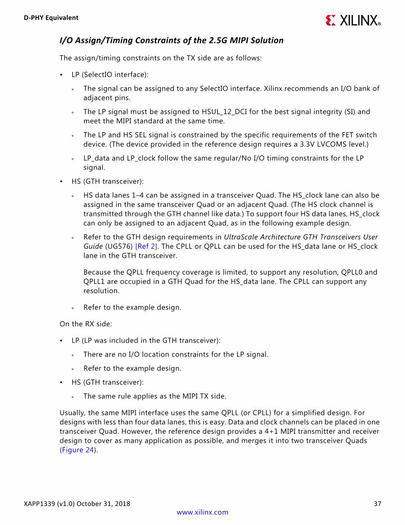
b. Set the Transceiver-based IP Debug Ports section (Figure 33).X-Ref Target - Figure 33
Figure 33: Transceiver-based IP Debug Ports Section
X21745-101118

D-PHY Equivalent
XAPP1339 (v1.0) October 31, 2018 47www.xilinx.com
c. Set the UG576/UG578 Chapter 2 - Reference Clock Selection and Distribution Ports section (Figure 34).
X-Ref Target - Figure 34
Figure 34: UG576/UG578 Chapter 2 - Reference Clock Selection and Distribution Ports Section
X21746-101118

D-PHY Equivalent
XAPP1339 (v1.0) October 31, 2018 48www.xilinx.com
d. Set the UG576/UG578 Chapter 2 - Quad PLL Ports, Reset and Initialization Ports, and CPLL Reset Ports sections (Figure 35).
X-Ref Target - Figure 35
Figure 35: UG576/UG578 Chapter 2 - Quad PLL Ports, Reset and Initialization Ports, and CPLL Reset Ports Sections
X21747-101118

D-PHY Equivalent
XAPP1339 (v1.0) October 31, 2018 49www.xilinx.com
e. Set the UG576/UG578 Chapter 2 - QPLL0/1 Reset Ports, TX Initialization and Reset Ports, RX Initialization and Reset Ports, and Power Down Ports sections (Figure 36).
X-Ref Target - Figure 36
Figure 36: UG576/UG578 Chapter 2 - QPLL0/1 Reset Ports, TX Initialization and Reset Ports, RX Initialization and Reset Ports, and Power Down Ports Sections
X21748-101118

D-PHY Equivalent
XAPP1339 (v1.0) October 31, 2018 50www.xilinx.com
f. Set the UG576/UG578 Chapter 2 - Loopback ports, Dynamic Reconfiguration Ports, FPGA TX Interface Ports, TX 8B/10B Encoder Ports, and TX Synchronous Gearbox Ports sections (Figure 37).
X-Ref Target - Figure 37
Figure 37: UG576/UG578 Chapter 2 - Loopback ports, Dynamic Reconfiguration Ports, FPGA TX Interface Ports, TX 8B/10B Encoder Ports, and TX Synchronous Gearbox Ports Sections
X21749-101118

D-PHY Equivalent
XAPP1339 (v1.0) October 31, 2018 51www.xilinx.com
g. Set the UG576/UG578 Chapter 3 - TX Asynchronous Gearbox Ports, TX Buffer Ports, TX Pattern Generator Ports, and TX Polarity Control Ports sections (Figure 38).
X-Ref Target - Figure 38
Figure 38: UG576/UG578 Chapter 3 - TX Asynchronous Gearbox Ports, TX Buffer Ports, TX Pattern Generator Ports, and TX Polarity Control Ports Sections
X21750-101118

D-PHY Equivalent
XAPP1339 (v1.0) October 31, 2018 52www.xilinx.com
h. Set the UG576/UG578 Chapter 3 - TX Fabric Clock Output Control Ports, TX Phase Interpolator PPM Controller Ports, and TX Configurable Driver Ports sections (Figure 39).
X-Ref Target - Figure 39
Figure 39: UG576/UG578 Chapter 3 - TX Fabric Clock Output Control Ports, TX Phase Interpolator PPM Controller Ports, and TX Configurable Driver Ports Sections
X21751-101118

D-PHY Equivalent
XAPP1339 (v1.0) October 31, 2018 53www.xilinx.com
i. Set the UG576/UG578 Chapter 3 - TX Out-of-Band Signaling Ports and Chapter 4 - RX Analog Front End Ports sections (Figure 40).
X-Ref Target - Figure 40
Figure 40: UG576/UG578 Chapter 3 - TX Out-of-Band Signaling Ports and Chapter 4 - RX Analog Front End Ports Sections
X21752-101118

D-PHY Equivalent
XAPP1339 (v1.0) October 31, 2018 54www.xilinx.com
j. Set the UG576/UG578 Chapter 4 - RX Equalizer (DFE and LPM) Ports section (Figure 41).X-Ref Target - Figure 41
Figure 41: UG576/UG578 Chapter 4 - RX Equalizer (DFE and LPM) Ports Section
X21753-101118

D-PHY Equivalent
XAPP1339 (v1.0) October 31, 2018 55www.xilinx.com
k. Set the Chapter 4 - RX CDR Ports section (Figure 42).X-Ref Target - Figure 42
Figure 42: Chapter 4 - RX CDR Ports Section
X21754-101118

D-PHY Equivalent
XAPP1339 (v1.0) October 31, 2018 56www.xilinx.com
l. Set the Chapter 4 - RX Byte and Word Alignment Ports section (Figure 43).X-Ref Target - Figure 43
Figure 43: Chapter 4 - RX Byte and Word Alignment Ports Section
X21755-101118

D-PHY Equivalent
XAPP1339 (v1.0) October 31, 2018 57www.xilinx.com
m. Set the Chapter 4 - RX Clock Correction Ports section (Figure 44).
2.5 Gb/s GTH D-PHY Custom Design and GTH Transceiver Migration Guidelines
To customize the MIPI design (number of MIPI channels or GTH placement) based on this reference design, read the following carefully before modifying the code.
GTH Reference Clock Configuration
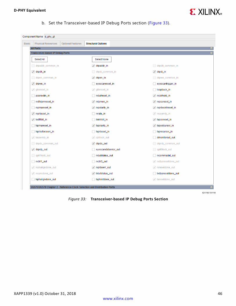
USER TOP (KCU105 loop TOP) contains the code shown in Figure 45. The following configuration is according to the clock solution of the example design of the KCU105 demo board. Customers need to modify the parameters based on the location of the GTH transceiver on the board [Ref 2].
X-Ref Target - Figure 44
Figure 44: Chapter 4 - RX Clock Correction Ports Section
X21756-101118

D-PHY Equivalent
XAPP1339 (v1.0) October 31, 2018 58www.xilinx.com
RX/TX 5lane Module
To support a wide range of design requirements, the reference design provides a fixed 4 data lane + 1 clock lane MIPI TX and RX data processing module connected to the MIPI D-PHY PCS layer. Each transceiver module maps to five standard GTH lanes named the RX/TX 5lane module. This module is provided in the netlist.
You can generate GTH modules according to the method described in Implementing the 2.5G Transceiver D-PHY Reference Design, customize the number of MIPI interface data lanes (data lane < 4), and connect RX/TX 5lane modules through the logical channel adaptation layer. When the number of data lanes is less than 4, the Vivado tools compile automatically to optimize those channels by processing unused data channel ports on RX/TX 5lane.
Logical Channel Adaptation Layer between MIPI TX/RX5 Lane Module and GTH Transceiver
The data lane of the MIPI interface is sorted from D0 to DN. The RX/TX 5lane’s data lane is also sorted in this lane order, mapping one-to-one with the MIPI interface data.
To simplify the mapping relationship between the RX/TX 5lane data and clock lanes and the transceiver physical lane, and to separate the transmitter and receiver channels from the GTH transceiver (which must include both transmitter and receiver channels when the GTH transceiver IP is generated), some HDL code is added between GTH_PHY_TOP.v and GTH_transceiver_example_wrapper.v to implement a logical channel adaptation layer.
X-Ref Target - Figure 45
Figure 45: GTH Reference Clock Configuration in HDL Code
X21684-100418
D-PHY Equivalent
XAPP1339 (v1.0) October 31, 2018 59www.xilinx.com
In this adapter layer, N (N < 8) independent logical channels are set up, and these N logical channels are divided into two logical Quads, which are numbered in HDL code. Logical channels 0–3 (Q0 0–3) are included by logical Q0. Logical channels 4–7 (Q1 0–3) are contained by logical Q1. The logical Quad has a mapping relationship with the physical transceiver Quad in code, and the logical channel also has a mapping relationship with the physical transceiver channel. In the HDL code, an example of a logical Quad is shown in Figure 46.
Note: Between the external MIPI interface data lane N to 0 and FPGA internal MIPI TX/RX 5lane modules data lane N to 0, the data lane has a strict one-to-one correspondence from N to 0.
X-Ref Target - Figure 46
Figure 46: Logical Quad in HDL Code
X21685-100418

D-PHY Equivalent
XAPP1339 (v1.0) October 31, 2018 60www.xilinx.com
Figure 47 describes the logical architecture of the channel adaptation layer in the reference design.
On the GTH transceiver side, depending on the number of MIPI interface data lanes on the PCB and design requirements, the physical location of the GTH transceiver can first be assigned, and then the XDC constraints can be used to map between the GTH transceiver and logical channels. See the constraint in Figure 49. The MIPI TX/RX 5lane module lane D0 to DN and MIPI interface D0 to DN are re-mapped by logical channel adaptation layer within the FPGA.
The behavior of the MIPI data and clock lanes is equivalent to the logic channel adaptation layer. However, the MIPI data lane has multiple lanes and a fixed lane number corresponding to the 5lane module data lane, so usually, the MIPI data lane is constrained first, followed by the MIPI clock lane on the GTH transceiver.
After determining the GTH transceiver position, the transceiver Quad location corresponding to logical Q needs to be determined to configure the reference clock source. Figure 48 is a mapping relation taking the KCU105 reference design as an example. (For GTH mapping refer to Figure 24.) The figure shows MIPI TX 4 data lane + 1 clock lane, and MIPI RX 4 data lane + 1 clock lane.
X-Ref Target - Figure 47
Figure 47: Logical Architecture of Channel Adaptation Layer in Reference Design
FPGA
Gth_phy_topPhy_gt_example_wrapper
TX 5LaneDN data lane
N ≤ 3D0 data lane
+clock lane
RX 5LaneDN data lane
N ≤ 3D0 data lane
+clock lane
N logic lane adaptation(N ≤ 8)
Q1
Q0
GTH
I/O
QuadXX
QuadXX+1
External PCB
MIPI interface (N ≤ 4)RX/TX N lane data + 1 lane clock
MIPI TX Clock
MIPI TX data DN
MIPI TX data D0
MIPI RX Clock
MIPI RX data DN
MIPI RX data D0
X21678-100418

D-PHY Equivalent
XAPP1339 (v1.0) October 31, 2018 61www.xilinx.com
1. The MIPI interface TX is assigned to 4X GTH of a transceiver Quad, and RX4 data lane is assigned to other 4X GTH of a transceiver Quad. In the reference design, the MIPI RX interface is connected to logical channels 0–3 (Q0 0–3) of the logical Q0, and the MIPI interface TX is connected to the Q0 logical channels 4–7 (Q1 0–3). On the other side of the logical channel, to correctly connect the MIPI interface data lane D0–D3 to the TX/RX 5lane data lane D0–D3, the RX 5lane module data lane connects to logical channels 0–3 (Q0–3), and the TX 5lane module data lane connects to logical channels 4–7 (Q1 0–3).
2. In the reference design, the MIPI RX clock lane and MIPI TX data lane share a GTH transceiver, while the MIPI TX clock lane and MIPI RX data lane share a GTH transceiver. Because the data lane determines the logical channel for the transceiver, the clock lane has the same logical channel number as the shared GTH data lane. The MIPI RX clock in the reference design is projected to logical lane 6 (Q1 2), so the clock in the RX 5lane module needs to be connected to logical lane 6. TX clocks are projected to logical lane 3 (Q0 3), and then the clock lane of the TX 5lane module needs to be connected to logical lane 3 (adapted according to the KCU105 demo board design).
3. Modify the MIPI_TX_USED and MIPI_RX_USED parameters in GTH_PHY_TOP.v to enable the corresponding DRP CH. In the KCU105 reference design:
MIPI_TX_USED = 8'b11111000
MIPI_RX_USED = 8'b01001111
4. In the KCU105 reference design, logic Q0 corresponds to Quad228, and Q1 corresponds to Quad227. If the reference clock is output from Quad228, connect the QPLL/CPLL on each GTH Quad to Refreclk0/Refreclk1 and SouthRef0/SouthRef1 in the HDL code.
X-Ref Target - Figure 48
Figure 48: Mapping Relation of KCU105 Reference Design
Gth_phy_top
Phy_gt_example_wrapper
TX 5LaneDN data lane
N ≤ 3D0 data lane
+clock lane
RX 5LaneDN data lane
N ≤ 3D0 data lane
+clock lane
N logic lane adaptation (N ≤ 8)
Q1
Q0
GTH
I/O
Quad227
Quad228
MIPI interfaceRX/TX 4 lane data + 1 lane clock
MIPI TX Clock MIPI RX Clock
TX channel 7 RX channel 7
TX channel 6 RX channel 6
TX channel 5 RX channel 5
TX channel 4 RX channel 4
TX channel 3 RX channel 3
TX channel 2 RX channel 2
TX channel 1 RX channel 1
TX channel 0 RX channel 0
MIPI TX data D3 MIPI RX data D3
MIPI TX data D2 MIPI RX data D2
MIPI TX data D1 MIPI RX data D1
MIPI TX data D0 MIPI RX data D0
X21679-100418

D-PHY Equivalent
XAPP1339 (v1.0) October 31, 2018 62www.xilinx.com
5. Add constraints in the XDC to implement MIPI data lane (the MIPI interface connects to the GTH transceiver) and FPGA logic channel mapping.
Based on this mapping method, customers can customize GTH mapping by modifying the source code (Figure 50). For example, you can place four MIPI TX data lanes on the GTH transceiver channel shared by the transceiver Quad where the MIPI RX data lane is located. The MIPI TX clock lane is placed in the MIPI RX clock lane to share a GTH transceiver channel. The DHL code needs to be modified in the reference design to connect the TX 5lane module data lane to TX logical channels 0–3 (Q0–3), TX 5lane module clock lane to TX logical channel 6 (Q1 2), and RX 5Lane needs no change. The corresponding DRP module enabling parameters and related reset chains should be modified as shown below:
MIPI_TX_USED = 8'b01001111
MIPI_RX_USED = 8'b01001111
Update the XDC with the new TX GTH location. At the same time, the location of the transceiver Quad has changed, and the clock parameters of the logical Q0 and Q1 in the code must be modified accordingly.
X-Ref Target - Figure 49
Figure 49: GTH Mapping to PCB
X21686-100418

D-PHY Equivalent
XAPP1339 (v1.0) October 31, 2018 63www.xilinx.com
GTH DRP Chain
Referring to Figure 51, the GTH PHY TOP contains N (N < 8) DRP channel control units and two DRP common control units to support a multiple line rate MIPI interface. In the RX 5Lane module, there is a DRP control module for CDR five times oversampling. All the design requirements of the DRP control module can be referred to UltraScale Architecture GTH Transceivers User Guide (UG576) [Ref 2].
IMPORTANT: If you redefine the MIPI channel number and change the GTH transceiver placement based on the reference design, you also need to modify the DRP chain.
Note: The DRP channel module is optional in MIPI fixed-line rate mode, but the DRP common module is required.
X-Ref Target - Figure 50
Figure 50: Mapping Relation of a Customize Design Example
Gth_phy_top
Phy_gt_example_wrapper
TX 5LaneDN data lane
N ≤ 3D0 data lane
+clock lane
RX 5LaneDN data lane
N ≤ 3D0 data lane
+clock lane
N logic lane adaptation (N ≤ 8)
Q1
Q0
GTH
I/O
Quad227
Quad228
MIPI interface RX/TX 4 lane data + 1 lane clock
MIPI TX Clock MIPI RX Clock
TX channel 7 RX channel 7
TX channel 6 RX channel 6
TX channel 5 RX channel 5
TX channel 4 RX channel 4
TX channel 3 RX channel 3
TX channel 2 RX channel 2
TX channel 1 RX channel 1
TX channel 0 RSX channel 0
MIPI TX data D3 MIPI RX data D3
MIPI TX data D2 MIPI RX data D2
MIPI TX data D1 MIPI RX data D1
MIPI TX data D0 MIPI RX data D0
X21680-100418
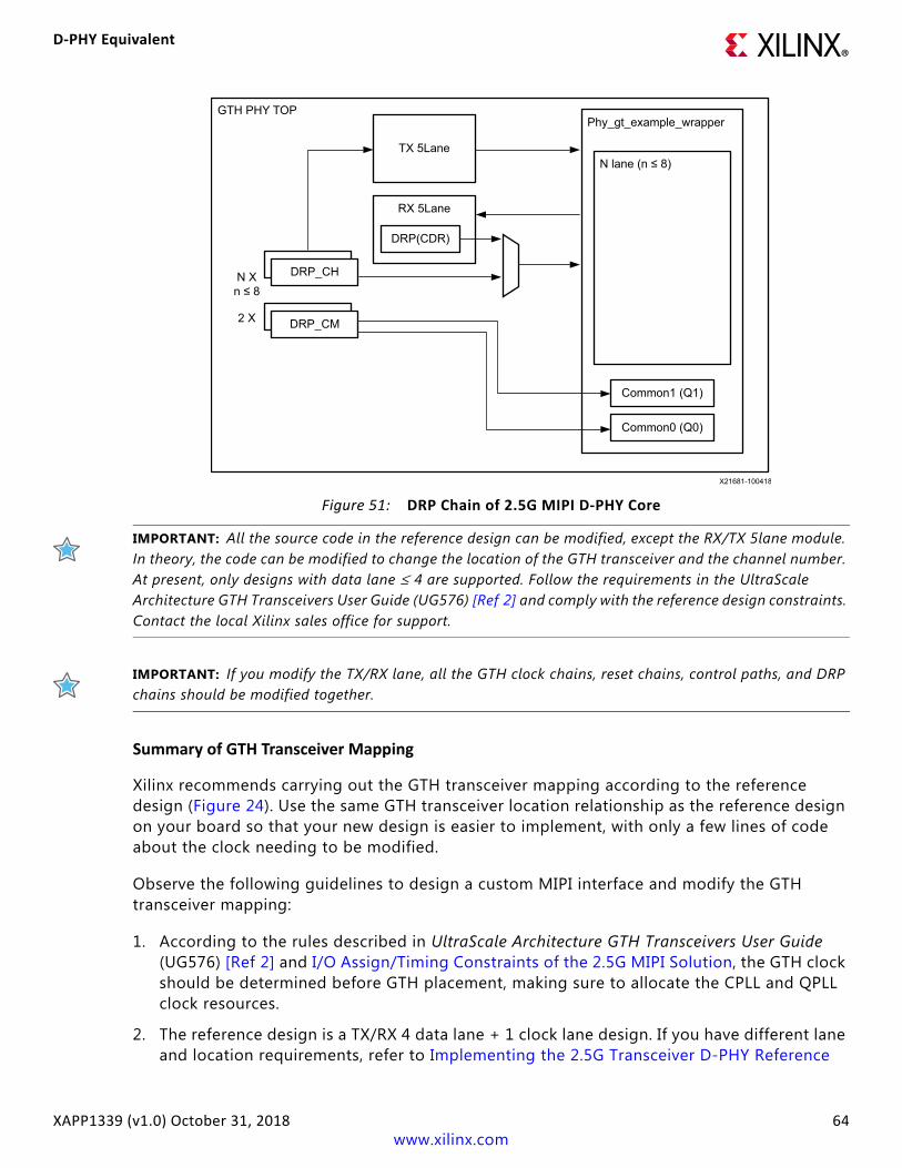
D-PHY Equivalent
XAPP1339 (v1.0) October 31, 2018 64www.xilinx.com
IMPORTANT: All the source code in the reference design can be modified, except the RX/TX 5lane module. In theory, the code can be modified to change the location of the GTH transceiver and the channel number. At present, only designs with data lane ≤ 4 are supported. Follow the requirements in the UltraScale Architecture GTH Transceivers User Guide (UG576) [Ref 2] and comply with the reference design constraints. Contact the local Xilinx sales office for support.
IMPORTANT: If you modify the TX/RX lane, all the GTH clock chains, reset chains, control paths, and DRP chains should be modified together.
Summary of GTH Transceiver Mapping
Xilinx recommends carrying out the GTH transceiver mapping according to the reference design (Figure 24). Use the same GTH transceiver location relationship as the reference design on your board so that your new design is easier to implement, with only a few lines of code about the clock needing to be modified.
Observe the following guidelines to design a custom MIPI interface and modify the GTH transceiver mapping:
1. According to the rules described in UltraScale Architecture GTH Transceivers User Guide (UG576) [Ref 2] and I/O Assign/Timing Constraints of the 2.5G MIPI Solution, the GTH clock should be determined before GTH placement, making sure to allocate the CPLL and QPLL clock resources.
2. The reference design is a TX/RX 4 data lane + 1 clock lane design. If you have different lane and location requirements, refer to Implementing the 2.5G Transceiver D-PHY Reference
X-Ref Target - Figure 51
Figure 51: DRP Chain of 2.5G MIPI D-PHY Core
GTH PHY TOP
TX 5Lane
DRP_CHDRP_CH
DRP_CHDRP_CM
N Xn ≤ 8
2 X
RX 5Lane
DRP(CDR)
Phy_gt_example_wrapper
N lane (n ≤ 8)
Common1 (Q1)
Common0 (Q0)
X21681-100418
D-PHY Equivalent
XAPP1339 (v1.0) October 31, 2018 65www.xilinx.com
Design to regenerate the GTH IP based on the reference design, then modify the HDL code to connect to the TX/RX 5lane module.
3. The modules related to GTH mapping provide customers with open source code, namely, the User_top (KCU105_loop_top.v), Gth_Phy_top.v, and Phy_gt_example_wrapper modules. Users need to modify the GTH port mapping, reset chain, and DRP interface according to the reference design.
Multi-Protocol Migration
The 2.5G transceiver D-PHY solution is flexible in the selection of QPLL or CPLL. At the same time, the reference design can flexibly extract all the transceiver ports that are not used at the MIPI level. Thus, it is possible to migrate the 2.5G transceiver D-PHY design to the same eight lanes as the transceiver interface of other protocols. Attention should be paid to the following:
• The key point is how to design a clock system, such as in Figure 52.

D-PHY Equivalent
XAPP1339 (v1.0) October 31, 2018 66www.xilinx.com
• Define the use of the DRP interface, and understand the DRP control chain of the reference design. Whether or not other protocol transceiver interfaces need to use DRP, such as when using DRP, you must consider how to time-share DRP ports with MIPI interfaces.
• According to the designed clock system, modifying the open HDL code and the reset chain design is very critical.
X-Ref Target - Figure 52
Figure 52: A Complex Customer Design Transceiver Mapping and GTH Transceiver Clock Solution Example (UltraScale FPGAs)
RX_CHANNEL0CLK_SEL
CPLL0~2
REFCLK1
TX_CHANNEL0
QPLL0/1
RX_CHANNEL1
RX_CHANNEL2
RX_CHANNEL3
TX_CHANNEL1
TX_CHANNEL2
TX_CHANNEL3
CLK_SEL
HDMI0 RX/5.94GHDMI0_CLK_297M
VbyOne_REF_148.5M REFCLK0
CPLL3
Vbyone TX/2.97G
RX_CHANNEL0
CLK_SEL QPLL0,1SOUTHREF1
TX_CHANNEL0CPLL0~
3
RX_CHANNEL1
RX_CHANNEL2
RX_CHANNEL3
TX_CHANNEL1
TX_CHANNEL2
TX_CHANNEL3
CLK_SEL
MIPI RX DATA/2.5G
MIPI_REFCLK_250M
SOUTHREF0
Vbyone TX/2.97G
CLK_SELSOUTHREF1MIPI RX HSCLK/1.25G
RX_CHANNEL0CLK_SEL QPLL0,1REFCLK1
TX_CHANNEL0
CPLL0,1,2
RX_CHANNEL1
RX_CHANNEL2
RX_CHANNEL3
TX_CHANNEL1
TX_CHANNEL2
TX_CHANNEL3
CLK_SEL
MIPI RX DATA/2.5G
SOUTHREF0
RX_CHANNEL0
CLK_SEL CPLL1,2,3
REFCLK1
TX_CHANNEL0
QPLL0,1
RX_CHANNEL1
RX_CHANNEL2
RX_CHANNEL3
TX_CHANNEL1
TX_CHANNEL2
TX_CHANNEL3
CLK_SELREFCLK0
MIPI TX HSCLK/750M
MIPI TX DATA/1.5GHDMI1 RX/5.94G
MIPI RX HSCLK/1.25G
MIPI_REFCLK_150M
CPLL0CLK_SELNORTHREF1
HDMI1_OUT_TX_REF_297M
CLK_SEL CPLL3
REFCLK0HDBASE_TX_REF_297M
QUAD 228
QUAD 226
QUAD 225
QUAD 227
HDMI TX/5.94G
CPLL1,2,3CPLL1,2,3
CPLL0,1,2CPLL0,1,2
QPLL0,1
QPLL0,1
QPLL0,1
CPLL0~3
CPLL0~3CPLL0~3
QPLL0/1
CPLL0~2CPLL0~2
REFCLK0
NORTHREF0
HDMI_CLK_156.25M
X21674-100418

D-PHY Equivalent
XAPP1339 (v1.0) October 31, 2018 67www.xilinx.com
Porting the Design from UltraScale to UltraScale+ FPGAs
To port your design from UltraScale to UltraScale+ FPGAs, use an UltraScale+ FPGA D-PHY reference design. Hardware design rules fully comply with the UltraScale FPGA design requirements.
Note: The current UltraScale+ FPGA GTH transceiver clock system is more complex, and the UltraScale+ FPGA 2.5G MIPI D-PHY reference design currently does not support CPLL. This limitation must be taken into account when designing the GTH transceiver mapping to previous PCB designs.
PCB Design Guidelines1. Component placement:
The attenuation network resistors on the TX side must be close to the FET switch device, but the attenuation network resistors (see Figure 10) and the FET switch device can be placed at any location on the PCB.
2. Guidelines and recommendations:
For the PCB wiring of the HS section, refer to the requirements in the “Design of Transitions for High-Speed Signals” chapter of UltraScale Architecture PCB Design User Guide (UG583) [Ref 8] for optimizing the impedance continuity of the vias and pads.
There is no special requirement for the LP device.
3. Guidelines for insertion loss:
The GTH transceiver-based D-PHY supports TX pre-emphasis and RX equalization functions. TX pre-emphasis can support 0~6 dB insertion loss by setting the TXPOSTCURSOR[4:0] for line rates higher than 500 Mb/s. RX equalization functions can support 0~6 dB insertion loss by setting these attributes. (This is included in the reference design.)
For UltraScale FPGAs:
° RXDFELPM_KL_CFG0[15:9] = 0x40;
° RXLPM_KH_CFG0[15:9] = 0x40;
° RXLPM_GC_CFG[12:8] = 0x1F;
For UltraScale+ FPGAs:
° RXDFELPM_KL_CFG1[15:9] = 0x40;
° RXLPM_KH_CFG1[15:9] = 0x40;
° RXLPM_GC_CFG[15:9] = 0x1F;
Figure 53 shows eye diagrams of a data stream after 6 dB insertion loss (left) and after being processed by equalization circuits (right).

Reference Design
XAPP1339 (v1.0) October 31, 2018 68www.xilinx.com
Reference DesignDownload the reference design files for this application note from the Xilinx website.
Table 17 shows the reference design matrix.
X-Ref Target - Figure 53
Figure 53: Data Stream Eye Diagrams
X21707-100918
Table 17: Reference Design Matrix
Parameter Description
General
Developer name John Hu
Target devices UltraScale and UltraScale+ FPGAs
Source code provided Yes
Source code format
Design uses code and IP from existing Xilinx application note and reference designs or third party
MIPI CSI-2 RX and MIPI DSI-2 TX IP provided by Northwest Logic
Simulation
Functional simulation performed No
Timing simulation performed N/A
Test bench used for functional and timing simulations
No
Test bench format Verilog
Simulator software/version used Vivado tools 2018.2
SPICE/IBIS simulations N/A
Implementation
Synthesis software tools/versions used Vivado tools 2018.2

Reference Design
XAPP1339 (v1.0) October 31, 2018 69www.xilinx.com
2.5G MIPI D-PHY Design (Only for Simulation)Figure 54 shows the HDL hierarchy in the 2.5G MIPI D-PHY design. Prbs_any.v is used to generate and detect the test signal and is not necessary in the customer design. The 2.5G MIPI D-PHY design contains simulation files that support the simulation of MIPI HS signals.
Note: LP signal simulation is not supported by the 2.5G MIPI D-PHY design because the LP signal contains a handshake protocol and is managed by the MIPI MAC layer. You can integrate the 2.5G D-PHY design with MIPI CSI-2/MIPI DSI-2 IP to develop a demonstrable system on this hardware platform.
The following two subsystem demonstrations use these MIPI CSI-2 RX/MIPI DSI-2 TX IP cores from Xilinx IP partner Northwest Logic.
Implementation software tools/versions used
Vivado tools 2018.2
Static timing analysis performed No
Hardware Verification
Hardware verified Yes
Hardware platform used for verification KCU105 evaluation board
X-Ref Target - Figure 54
Figure 54: HDL Hierarchy in 2.5G MIPI D-PHY Design
Table 17: Reference Design Matrix (Cont’d)
Parameter Description
X21732-101018

Reference Design
XAPP1339 (v1.0) October 31, 2018 70www.xilinx.com
Hardware Platform
To build a 2.5G MIPI demonstration platform, you require a KCU105 board [Ref 9] or ZCU102 board [Ref 10] with an Avnet 2.5G MIPI development suite (card number: ADX=FMC-MIPI2.5G). shows an overview of the hardware platform.
X-Ref Target - Figure 55
Figure 55: Hardware Platform Overview
X21710-100918

Reference Design
XAPP1339 (v1.0) October 31, 2018 71www.xilinx.com
The Avnet 2.5G MIPI development suite contains several sub-cards:
• Avnet 2.5G MIPI FMC card (Figure 55).
Note: MIPI TX and RX connectors are included on this board. Each connector supports connections to MIPI CSI-2 or MIPI DSI-2 interfaces.
X-Ref Target - Figure 56
Figure 56: Avnet 2.5G MIPI FMC Card
X21711-100918

Reference Design
XAPP1339 (v1.0) October 31, 2018 72www.xilinx.com
• MIPI camera display adapter cards (Figure 57).X-Ref Target - Figure 57
Figure 57: MIPI Camera Adapter Card (Left) and Display Adapter Card (Right)
X21713-101018

Reference Design
XAPP1339 (v1.0) October 31, 2018 73www.xilinx.com
• MIPI loopback adapter card (Figure 58).X-Ref Target - Figure 58
Figure 58: MIPI Loopback Adapter Card
X21733-101018

Reference Design
XAPP1339 (v1.0) October 31, 2018 74www.xilinx.com
2.5G MIPI Subsystem in Pass-through ModeFigure 59 shows the 2.5G MIPI subsystem in pass-through mode.
To run this demo, you require the KCU105 board, Avnet 2.5G MIPI FMC card, Avnet MIPI camera adapter card, and MIPI display adapter card. The video stream generated by the MIPI camera adapter card is sent to the MIPI DSI-2 TX (on the Avnet 2.5G MIPI FMC card) and HDMI™ interface (on the KCU105 board) simultaneously through the MIPI CSI-2 RX interface (on the Avnet 2.5G MIPI FMC card). The DSI-2 TX can also be switched to send a fixed video pattern from the Test Pattern Generator module.
Note: For more information about how to set up the demo, see the readme.txt in the reference design ZIP file.
Running the 2.5G MIPI Subsystem Demo in Pass-through Mode on the KCU105 Board
Xilinx only provides the bit file for the demo (limited by the Northwest Logic IP license agreement). You can build the demo quickly using the hardware platform and programming the FPGA on the KCU105 board with the bit file.
Note: For more information about the 2.5G MIPI subsystem hardware and logic design, contact Avnet and Northwest Logic.
X-Ref Target - Figure 59
Figure 59: 2.5G MIPI Subsystem in Pass-through Mode
KCU105 2.5G MIPI Pass-through
DDR4 MIG
MicroBlaze Processor
VDMA Write VDMA Read VDMA Read
HDMI PIPE 12C &UART GPIO
OV13855 MIPI Panel Monitor
MIPI CSI-2 Peripheral MIPI DSI-2 Host
GTH Transceiver D-PHY
540 Mb/s/lane or1080 Mb/s/lane 800 Mb/s/lane
AXI4-Lite
AXI4-Lite AXI4-Lite
AXI4-Lite
AXI4 AXI4 AXI4
AXI4-LiteAXI4-LiteAXI4-Lite
X21714-102318

Reference Design
XAPP1339 (v1.0) October 31, 2018 75www.xilinx.com
2.5G Subsystem Design in Loopback ModeFigure 59 shows the 2.5G MIPI subsystem in loopback mode.
To run this demo, you require the KCU105 board, Avnet 2.5G MIPI FMC card, and MIPI loopback adapter. It is currently difficult to find a 2.5G MIPI interface camera in the market, so the loopback card was provided by the Avnet 2.5G MIPI development suite. This was used to connect the MIPI RX and DSI TX on the FMC board directly for the 2.5G MIPI loopback test.
Note: For more information about how to set the demo, read the readme.txt in the reference design ZIP file.
Running the 2.5G MIPI Subsystem in Loopback Mode on the KCU105 Board
Xilinx only provides the bit file for the demo (limited by the Northwest Logic license agreement). You can build the demo quickly using the hardware platform and programming the FPGA on the KCU105 board with the bit file.
Note: For more information about the 2.5G MIPI subsystem hardware and logic design, contact Avnet and Northwest Logic.
KCU105 Board FMCH VADJ Adjustment
The 2.5G MIPI FMC’s intelligent platform management interface (IPMI) can make the KCU105 board adjust the VDJ automatically so that users do not need to make any adjustments.
X-Ref Target - Figure 60
Figure 60: 2.5G MIPI Subsystem in Loopback Mode
KCU105 2.5G MIPI Pass-through
Error Reporting
MicroBlaze Processor
MIPI Test Pattern Generator
GPIO 12C &UART
Loopback Adapter
MIPI DSI-2 Peripheral MIPI DSI-2 Host
GTH Transceiver D-PHY
2.5 Gb/s/lane
AXI4-Lite AXI4-Lite
X21736-102318

Conclusion
XAPP1339 (v1.0) October 31, 2018 76www.xilinx.com
ConclusionThe use of simple external circuits, such as those presented in this application note, make it possible to connect an FPGA to an ASSP device via its MIPI interface, supporting up to 2.5G.
Documentation Navigator and Design HubsXilinx® Documentation Navigator provides access to Xilinx documents, videos, and support resources, which you can filter and search to find information. To open the Xilinx Documentation Navigator (DocNav):
• From the Vivado® IDE, select Help > Documentation and Tutorials.
• On Windows, select Start > All Programs > Xilinx Design Tools > DocNav.
• At the Linux command prompt, enter docnav.
Xilinx Design Hubs provide links to documentation organized by design tasks and other topics, which you can use to learn key concepts and address frequently asked questions. To access the Design Hubs:
• In the Xilinx Documentation Navigator, click the Design Hubs View tab.
• On the Xilinx website, see the Design Hubs page.
Note: For more information on Documentation Navigator, see the Documentation Navigator page on the Xilinx website.
References1. MIPI Alliance specification for D-PHY
http://mipi.org/specifications/physical-layer
2. UltraScale Architecture GTH Transceivers User Guide (UG576)
3. MIPI D-PHY v4.1 Product Guide (PG202)
4. D-PHY Solutions (XAPP894)
5. Scalable Low-Voltage Signaling for 400 mV: JESD 8-13 https://www.jedec.org/standards-documents/docs/jesd-8-13
6. Kintex UltraScale FPGAs Data Sheet: DC and AC Switching Characteristics (DS892)
7. Kintex UltraScale+ FPGAs Data Sheet: DC and AC Switching Characteristics (DS922)
8. UltraScale Architecture PCB Design User Guide (UG583)
9. Xilinx Kintex UltraScale FPGA KCU105 Evaluation Kit https://www.xilinx.com/products/boards-and-kits/kcu105.html

Revision History
XAPP1339 (v1.0) October 31, 2018 77www.xilinx.com
10. Xilinx Zynq UltraScale+ MPSoC ZCU102 Evaluation Kit https://www.xilinx.com/products/boards-and-kits/ek-u1-zcu102-g.html
11. Avnet ADX=FMC-MIPI2.5G sub-cardhttps://www.avnet.com/wps/portal/apac
Revision HistoryThe following table shows the revision history for this document.
Please Read: Important Legal NoticesThe information disclosed to you hereunder (the “Materials”) is provided solely for the selection and use of Xilinx products. To the maximum extent permitted by applicable law: (1) Materials are made available “AS IS” and with all faults, Xilinx hereby DISCLAIMS ALL WARRANTIES AND CONDITIONS, EXPRESS, IMPLIED, OR STATUTORY, INCLUDING BUT NOT LIMITED TO WARRANTIES OF MERCHANTABILITY, NON-INFRINGEMENT, OR FITNESS FOR ANY PARTICULAR PURPOSE; and (2) Xilinx shall not be liable (whether in contract or tort, including negligence, or under any other theory of liability) for any loss or damage of any kind or nature related to, arising under, or in connection with, the Materials (including your use of the Materials), including for any direct, indirect, special, incidental, or consequential loss or damage (including loss of data, profits, goodwill, or any type of loss or damage suffered as a result of any action brought by a third party) even if such damage or loss was reasonably foreseeable or Xilinx had been advised of the possibility of the same. Xilinx assumes no obligation to correct any errors contained in the Materials or to notify you of updates to the Materials or to product specifications. You may not reproduce, modify, distribute, or publicly display the Materials without prior written consent. Certain products are subject to the terms and conditions of Xilinx’s limited warranty, please refer to Xilinx’s Terms of Sale which can be viewed at https://www.xilinx.com/legal.htm#tos; IP cores may be subject to warranty and support terms contained in a license issued to you by Xilinx. Xilinx products are not designed or intended to be fail-safe or for use in any application requiring fail-safe performance; you assume sole risk and liability for use of Xilinx products in such critical applications, please refer to Xilinx’s Terms of Sale which can be viewed at https://www.xilinx.com/legal.htm#tos.AUTOMOTIVE APPLICATIONS DISCLAIMERAUTOMOTIVE PRODUCTS (IDENTIFIED AS “XA” IN THE PART NUMBER) ARE NOT WARRANTED FOR USE IN THE DEPLOYMENT OF AIRBAGS OR FOR USE IN APPLICATIONS THAT AFFECT CONTROL OF A VEHICLE (“SAFETY APPLICATION”) UNLESS THERE IS A SAFETY CONCEPT OR REDUNDANCY FEATURE CONSISTENT WITH THE ISO 26262 AUTOMOTIVE SAFETY STANDARD (“SAFETY DESIGN”). CUSTOMER SHALL, PRIOR TO USING OR DISTRIBUTING ANY SYSTEMS THAT INCORPORATE PRODUCTS, THOROUGHLY TEST SUCH SYSTEMS FOR SAFETY PURPOSES. USE OF PRODUCTS IN A SAFETY APPLICATION WITHOUT A SAFETY DESIGN IS FULLY AT THE RISK OF CUSTOMER, SUBJECT ONLY TO APPLICABLE LAWS AND REGULATIONS GOVERNING LIMITATIONS ON PRODUCT LIABILITY.© Copyright 2018 Xilinx, Inc. Xilinx, the Xilinx logo, Artix, ISE, Kintex, Spartan, Virtex, Vivado, Zynq, and other designated brands included herein are trademarks of Xilinx in the United States and other countries. HDMI, HDMI logo, and High-Definition Multimedia Interface are trademarks of HDMI Licensing LLC. All other trademarks are the property of their respective owners.
Section Revision Summary
10/31/2018 Version 1.0
Initial Xilinx release. N/A