
Imperial College London Department of Physics
56
Imperial College London Department of Physics Graphene Field Effect Transistors By Mohamed Warda and Khodr Badih 20 July 2021 arXiv:2010.10382v2 [cond-mat.mes-hall] 20 Jul 2021
Transcript of Imperial College London Department of Physics
Imperial College London
Department of Physics
Graphene Field Effect Transistors
By Mohamed Warda and Khodr Badih
20 July 2021
arX
iv:2
010.
1038
2v2
[co
nd-m
at.m
es-h
all]
20
Jul 2
021
Abstract
The past decade has seen rapid growth in the research area of graphene and its
application to novel electronics. With Moore’s law beginning to plateau, the need
for post-silicon technology in industry is becoming more apparent. Moreover, exist-
ing technologies are insufficient for implementing terahertz detectors and receivers,
which are required for a number of applications including medical imaging and secu-
rity scanning. Graphene is considered to be a key potential candidate for replacing
silicon in existing CMOS technology as well as realizing field effect transistors for
terahertz detection, due to its remarkable electronic properties, with observed elec-
tronic mobilities reaching up to 2× 105 cm2 V−1 s−1 in suspended graphene sam-
ples. This report reviews the physics and electronic properties of graphene in the
context of graphene transistor implementations. Common techniques used to syn-
thesize graphene, such as mechanical exfoliation, chemical vapor deposition, and
epitaxial growth are reviewed and compared. One of the challenges associated with
realizing graphene transistors is that graphene is semimetallic, with a zero bandgap,
which is troublesome in the context of digital electronics applications. Thus, the
report also reviews different ways of opening a bandgap in graphene by using bi-
layer graphene and graphene nanoribbons. The basic operation of a conventional
field effect transistor is explained and key figures of merit used in the literature
are extracted. Finally, a review of some examples of state-of-the-art graphene field
effect transistors is presented, with particular focus on monolayer graphene, bilayer
graphene, and graphene nanoribbons.

Contents
Acronyms and Constants i
1 Introduction 1
1.1 Motivation . . . . . . . . . . . . . . . . . . . . . . . . . . . . . . . . . . . 1
1.2 Layout of Report . . . . . . . . . . . . . . . . . . . . . . . . . . . . . . . 3
2 Graphene 5
2.1 Crystallography and Band Structure . . . . . . . . . . . . . . . . . . . . 6
2.2 Physical Properties . . . . . . . . . . . . . . . . . . . . . . . . . . . . . . 14
2.3 Synthesis Techniques . . . . . . . . . . . . . . . . . . . . . . . . . . . . . 17
2.4 Related Structures and Bandgap Engineering . . . . . . . . . . . . . . . . 20
2.4.1 Bilayer Graphene . . . . . . . . . . . . . . . . . . . . . . . . . . . 21
2.4.2 Graphene Nanoribbons . . . . . . . . . . . . . . . . . . . . . . . . 23
3 Conventional CMOS Technology 27
4 State-of-the-Art Graphene FETs 32
4.1 Monolayer Graphene FETs . . . . . . . . . . . . . . . . . . . . . . . . . . 33
4.2 Bilayer Graphene FETs . . . . . . . . . . . . . . . . . . . . . . . . . . . 35
4.3 Graphene Nanoribbon FETs . . . . . . . . . . . . . . . . . . . . . . . . . 36
5 Conclusion and Future Perspectives 38
References 40
Appendix 46

Acronyms and Constants
Acronyms
CMOS Complementary metal oxide semiconductor
CNT Carbon nanotube
CVD Chemical vapor deposition
HEMT High electron mobility transistor
FET Field effect transistor
GNR Graphene nanoribbon
RF Radio Frequency
STM Scanning tunneling microscopy
i

Constants
i The imaginary unit,√−1
c The speed of light in vacuum, 3.00× 10⁻⁸ m s−1
e The elementary charge, 1.60× 10⁻¹⁹ C
h The Planck constant, 6.63× 10⁻³⁴ Js
~ The reduced Planck constant, h2π
ii
1 INTRODUCTION
1 Introduction
1.1 Motivation
Graphene is a two dimensional sheet of carbon atoms arranged in a honeycomb lattice.
Since its discovery in 2004 by Geim and Novoselov, for which they shared the Nobel prize
in 2010 [23], graphene has captured the interests of scientists and engineers alike. Due to
its two-dimensional nature, graphene possesses a myriad of novel electronic, mechanical,
thermal, and optical properties that make it a potential candidate for several applications
including flexible electronics, touch screens, biological and chemical sensing, drug delivery,
and transistors [22, 64, 45, 62, 16]. Indeed, the application of graphene to electronics is
now a burgeoning research area, and has come along way since its genesis in 2004.
The transistor is a key building block of virtually all modern electronic devices. The
first transistor was invented in 1947 by Shockley, Bardeen, and Brattain at Bell Labs,
and represented a revolutionary advancement in the development of electronic devices
in the latter half of the 20th century. Different types of transistors, including bipolar
junction transistors (BJTs) and field effect transistors (FETs) were invented in the 20th
century – but the most commonly used transistor in modern electronics is the metal oxide
semiconductor field effect transistor (MOSFET), which was invented by Atalla and Kahng
in 1959 at Bell Labs. Complementary metal oxide semiconductor (CMOS) technology
uses MOSFETs made primarily of silicon, and is the most widely used technology for
realizing electronics today [53, 55].
Since its inception, physicists and engineers have downscaled the size of the MOSFET
transistor while maintaining its performance, which has been the driving force behind the
incredible speed at which technology has progressed over the past few decades. In more
concrete terms, this is described by Moore’s law. Moore’s law is the observation that
the number of transistors on an integrated circuit (and, in turn, computer processing
power) doubles every two years at the same cost as a result of downscaling the size
of the MOSFET transistor [41, 24, 42]. Figure 1 depicts the number of transistors on
computer chips as a function of time, from 1965 to 2015, which can be seen to roughly
vary according to Moore’s law. As of 2019, the number of transistors on commercially
available microprocessors can reach up to 39.54 billion [1], and Samsung and TSMC have
been fabricating 10 nm and 7 nm MOSFETs [2, 3].
1

1 INTRODUCTION
Figure 1: A graphical illustration of Moore’s law from 1965 to 2015. The vertical axis,
showing the transistor count, is logarithmic. It is evident that, to a good
approximation, the number of transistors on a computer chip has doubled every two
years, for the past five decades [24].
Recently, however, it has been observed that Moore’s law is beginning to reach a
plateau, as the miniaturization of transistors continues, and is predicted to end around
2025 [4]. Moreover, the International Technology Roadmap for Semiconductors predicts
that after the year 2021, downscaling transistors will no longer be economically viable [5].
This is primarily because at small scales, undesirable short-channel effects such as drain
induced barrier lowering, velocity saturization, impact ionization, and other quantum
mechanical phenomena begin to manifest, degrading MOSFET performance [31]. As
such, physicists and engineers are considering alternative avenues and technologies for
extending Moore’s law in a post-silicon world. Among the chief novel materials that
provide a way of achieving this goal is graphene [22].
The remarkable electronic properties exhibited by graphene, including its extraordi-
2

1 INTRODUCTION
narily high mobility and its ambipolar field effect behavior, make it a promising candidate
for carrying electric current in FETs and could in principle outperform existing silicon-
based technologies [64, 22]. Since 2007, efforts have been made toward incorporating
graphene into existing MOSFET technology [6]. These graphene-based FETs have a
number of important potential engineering applications, including sensors [16, 19] and
high frequency terahertz detectors [29]. The latter is of particular importance in engi-
neering due to the so-called “terahertz gap” – a region in the electromagnetic spectrum
extending roughly from 0.1 THz to 10 THz for which existing generation/detection tech-
nologies are inadequate. Terahertz technology has a number of potential applications
including medical imaging, security scanning, and as a tool in molecular biology research
[29, 17, 59, 62]. However, there exist economic and physical challenges and bottlenecks
associated with realizing graphene FETs that are suitable for the aforementioned ap-
plications. This report provides a review of the physics of graphene and its electronic
properties as relevant in the context of field effect transistors as well as a state-of-the-art
review of different graphene FET implementations.
1.2 Layout of Report
The remainder of this report is split up into four main sections. In section 2, a brief his-
torical overview of graphene is presented, followed by a review of the physics of graphene
with particular emphasis on its crystallography and electronic band structure. Relevant
electronic properties, such as the high mobility of graphene and its ambipolar field effect
behavior, are described. Different methods of synthesizing graphene are presented and
compared in terms of their scalability, cost, and the quality of graphene production. Fi-
nally, the topic of bandgap engineering in graphene is discussed, using bilayer graphene
and graphene nanoribbons as examples.
In section 3, the principle of operation of the conventional MOSFET transistor is
discussed, and an overview of basic MOSFET device physics is presented. The MOSFET
transistor is modelled as a three terminal device, and relevant current-voltage character-
istics are highlighted. Key figures of merit that are commonly found in the literature are
extracted from the model, and are used in section 4 to compare different graphene FET
implementations.
In section 4, a state-of-the-art review of graphene FETs is presented, with particular
3
1 INTRODUCTION
focus on monolayer graphene FETs, bilayer graphene FETs, and graphene nanoribbon
FETs. Different implementations in the literature are compared using the figures of merit
presented in section 3, and the challenges associated with improving the performance of
graphene FETs are identified and discussed.
Finally, in section 5, the key ideas pertaining to the state-of-the-art graphene FETs
presented in section 4 are summarized, and an assessment of the current state of graphene
FET research within the wider context of modern industrial applications is presented.
4
2 GRAPHENE
2 Graphene
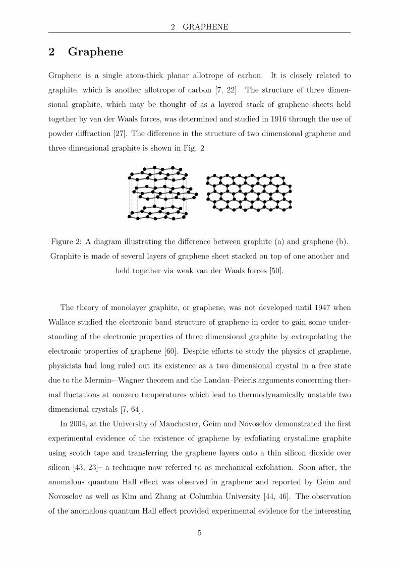
Graphene is a single atom-thick planar allotrope of carbon. It is closely related to
graphite, which is another allotrope of carbon [7, 22]. The structure of three dimen-
sional graphite, which may be thought of as a layered stack of graphene sheets held
together by van der Waals forces, was determined and studied in 1916 through the use of
powder diffraction [27]. The difference in the structure of two dimensional graphene and
three dimensional graphite is shown in Fig. 2
Figure 2: A diagram illustrating the difference between graphite (a) and graphene (b).
Graphite is made of several layers of graphene sheet stacked on top of one another and
held together via weak van der Waals forces [50].
The theory of monolayer graphite, or graphene, was not developed until 1947 when
Wallace studied the electronic band structure of graphene in order to gain some under-
standing of the electronic properties of three dimensional graphite by extrapolating the
electronic properties of graphene [60]. Despite efforts to study the physics of graphene,
physicists had long ruled out its existence as a two dimensional crystal in a free state
due to the Mermin-–Wagner theorem and the Landau–Peierls arguments concerning ther-
mal fluctations at nonzero temperatures which lead to thermodynamically unstable two
dimensional crystals [7, 64].
In 2004, at the University of Manchester, Geim and Novoselov demonstrated the first
experimental evidence of the existence of graphene by exfoliating crystalline graphite
using scotch tape and transferring the graphene layers onto a thin silicon dioxide over
silicon [43, 23]– a technique now referred to as mechanical exfoliation. Soon after, the
anomalous quantum Hall effect was observed in graphene and reported by Geim and
Novoselov as well as Kim and Zhang at Columbia University [44, 46]. The observation
of the anomalous quantum Hall effect provided experimental evidence for the interesting
5
2 GRAPHENE
relativistic behavior of electrons in graphene – in particular, it was shown that electrons in
graphene may be viewed as massless charged fermions [44]. As shall be explained in this
section, the relativistic behavior of electrons in graphene gives rise to its extraordinary
electronic properties.
2.1 Crystallography and Band Structure
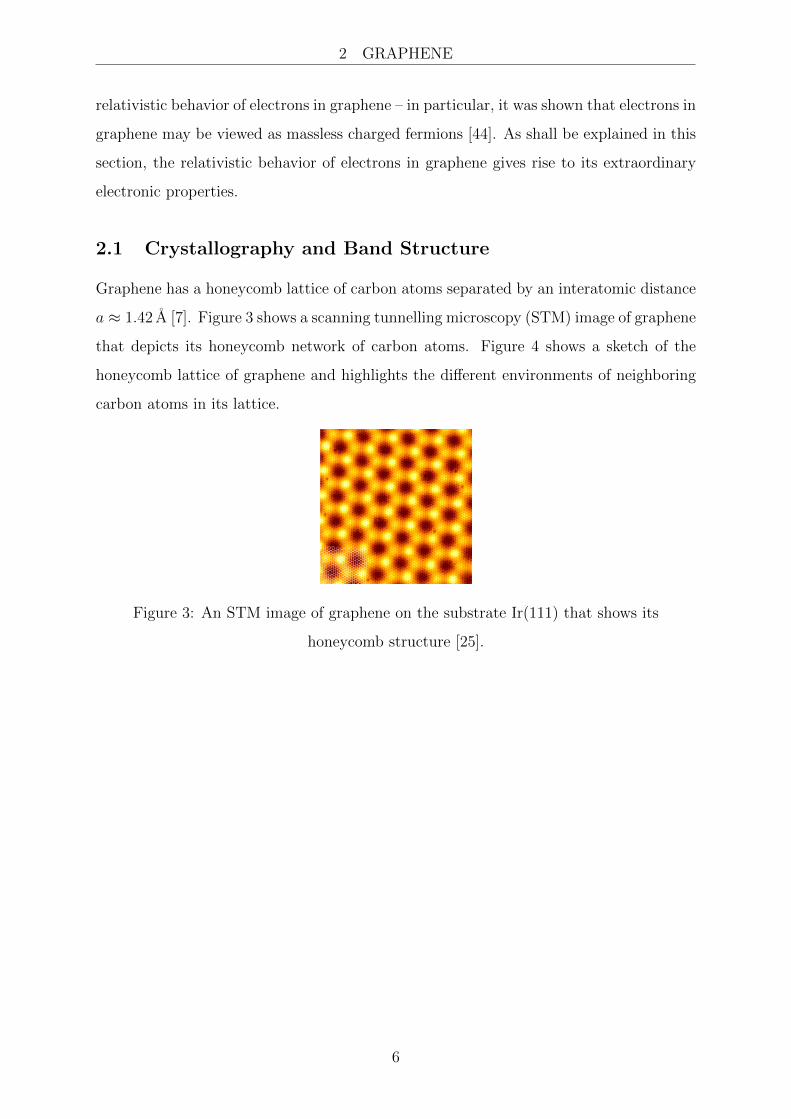
Graphene has a honeycomb lattice of carbon atoms separated by an interatomic distance
a ≈ 1.42�A [7]. Figure 3 shows a scanning tunnelling microscopy (STM) image of graphene
that depicts its honeycomb network of carbon atoms. Figure 4 shows a sketch of the
honeycomb lattice of graphene and highlights the different environments of neighboring
carbon atoms in its lattice.
Figure 3: An STM image of graphene on the substrate Ir(111) that shows its
honeycomb structure [25].
6

2 GRAPHENE
Figure 4: (a) The honeycomb lattice, with the primitive lattice vectors a1 and a2 that
span the lattice in real space. Different carbon atoms corresponding to filled and
unfilled circles are not equivalent in crystallographic terms, so the honeycomb lattice is
not a Bravais lattice. (b) Shows how this problem can be overcome by defining the
shaded region to be a unit cell containing two distinguishable carbon atoms. The two
atoms may be thought of as atoms from two different interpenetrating sublattices,
labelled A and B [7].
As shown in Fig. 4, different atoms in the lattice are not equivalent, making the
honeycomb lattice a non-Bravais lattice. These two inequivalent sublattices, labelled A
and B, may be thought of as interpentrating sublattices that form a triangular Bravais
lattice with two atoms per unit cell and two primitive lattice vectors a1 and a2 [7].
With reference to the coordinate system defined by the right-handed orthonormal set of
vectors (e1, e2, e3) is such that e1 and e2 lie in the plane of graphene, with e3 pointing in
a direction perpendicular to the plane. The primitive lattice vectors are given by
a1 =
√3a
2(e1 −
√3e2) =
a′
2(e1 −
√3e2) (1)
and
a2 =
√3a
2(e1 +
√3e2) =
a′
2(e1 +
√3e2), (2)
where ‖a1,2‖ = a′ =√
3a ≈ 2.46�A is the lattice constant. The primitive reciprocal lattice
vectors, b1 and b2, are related to a1 and a2 [55] by
b1 = 2πa2 × e3
a1 · (a2 × e3)=
2π
a′
(e1 −
e2√3
)(3)
7

2 GRAPHENE
and
b2 = 2πe3 × a1
a1 · (a2 × e3)=
2π
a′
(e1 +
e2√3
). (4)
Figure 5: The reciprocal lattice of graphene (in k space). The shaded region is the first
Brillouin zone, which is a Wigner–Seitz cell of the reciprocal lattice. By convention, Γ
denotes the point k = 0. The points M and M ′, as well as K and K ′, are inequivalent.
Equivalent points are separated in k space by b1 and b2. The corners of the first
Brillouin zone, namely, the six points labelled K and K ′, are collectively referred to as
Dirac points [7].
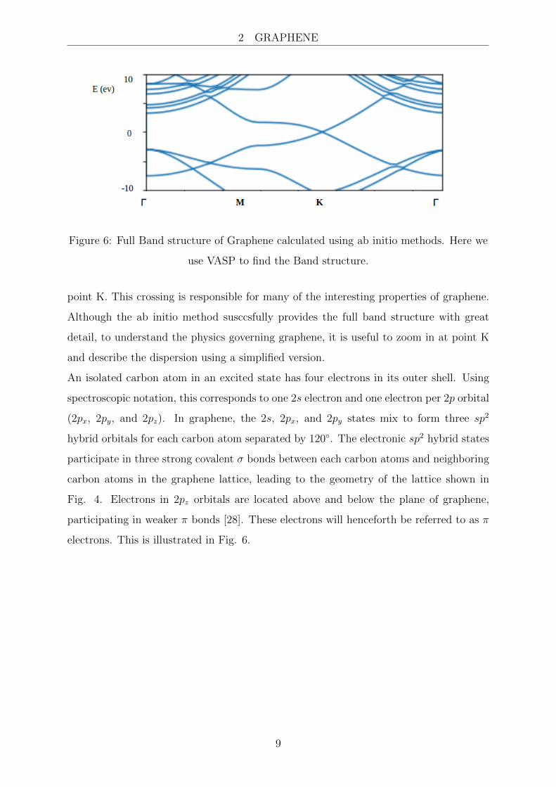
Figure 5 shows the first Brillouin zone for graphene in reciprocal space. The center of
the first Brillioin zone is labelled as Γ by convention and corresponds to the origin k = 0,
where k = (kx, ky) is the wave vector associated with electronic states in the lattice, with
kx and ky representing the wavenumbers along e1 and e2, respectively. The first Brillouin
zone is hexagonal and has six points labelled K and K ′, collectively referred to as Dirac
points. Points with the same label are considered to be equivalent and are separated
by a primitive reciprocal lattice vector (b1 or b2). The novel electronic properties of
graphene hinge on the excitations around these six Dirac points, as shall be explained
in this section. It is worth however, showing first the full band structure of graphene
computed from first principle calculations. We use VASP to find the full band structure
of Graphene. The results are presented in the graph below,
The interesting feature of the above band structure as we shall see below is the crossing at
8
2 GRAPHENE
Figure 6: Full Band structure of Graphene calculated using ab initio methods. Here we
use VASP to find the Band structure.
point K. This crossing is responsible for many of the interesting properties of graphene.
Although the ab initio method susccsfully provides the full band structure with great
detail, to understand the physics governing graphene, it is useful to zoom in at point K
and describe the dispersion using a simplified version.
An isolated carbon atom in an excited state has four electrons in its outer shell. Using
spectroscopic notation, this corresponds to one 2s electron and one electron per 2p orbital
(2px, 2py, and 2pz). In graphene, the 2s, 2px, and 2py states mix to form three sp2
hybrid orbitals for each carbon atom separated by 120◦. The electronic sp2 hybrid states
participate in three strong covalent σ bonds between each carbon atoms and neighboring
carbon atoms in the graphene lattice, leading to the geometry of the lattice shown in
Fig. 4. Electrons in 2pz orbitals are located above and below the plane of graphene,
participating in weaker π bonds [28]. These electrons will henceforth be referred to as π
electrons. This is illustrated in Fig. 6.
9
2 GRAPHENE
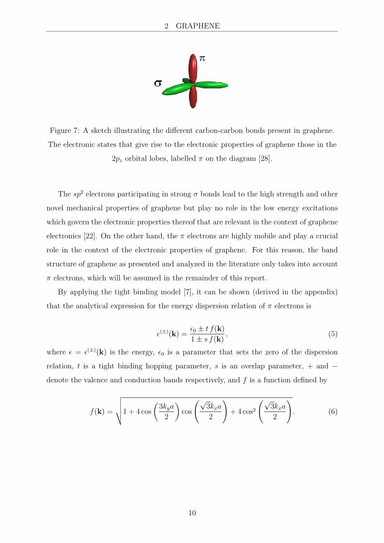
Figure 7: A sketch illustrating the different carbon-carbon bonds present in graphene.
The electronic states that give rise to the electronic properties of graphene those in the
2pz orbital lobes, labelled π on the diagram [28].
The sp2 electrons participating in strong σ bonds lead to the high strength and other
novel mechanical properties of graphene but play no role in the low energy excitations
which govern the electronic properties thereof that are relevant in the context of graphene
electronics [22]. On the other hand, the π electrons are highly mobile and play a crucial
role in the context of the electronic properties of graphene. For this reason, the band
structure of graphene as presented and analyzed in the literature only takes into account
π electrons, which will be assumed in the remainder of this report.
By applying the tight binding model [7], it can be shown (derived in the appendix)
that the analytical expression for the energy dispersion relation of π electrons is
ε(±)(k) =ε0 ± t f(k)
1± s f(k), (5)
where ε = ε(±)(k) is the energy, ε0 is a parameter that sets the zero of the dispersion
relation, t is a tight binding hopping parameter, s is an overlap parameter, + and −
denote the valence and conduction bands respectively, and f is a function defined by
f(k) =
√√√√1 + 4 cos
(3kya
2
)cos
(√3kxa
2
)+ 4 cos2
(√3kxa
2
). (6)
10

2 GRAPHENE
Figure 8: A Mathematica plot of the energy dispersion relation of graphene (Eq. (5)),
showing the valence (blue) and conduction (red) bands in the first Brillouin zone. The
valence and conduction bands touch at six points (the Dirac points) resulting in a zero
energy bandgap.
Figure 7 depicts surface plot of the valence (blue) and conduction (red) bands in the
first Brillouin zone in accordance with Eq. (5), using the values ε0 = 0, t = −3.033 eV,
and s = 0.129. The values for t and s were obtained from [49]. The band structure
shows that the valence and conduction bands of graphene coincide at six points (the
Dirac points of the reciprocal lattice), indicating a zero bandgap∗. Thus, graphene is
semimetallic. The six (Dirac) points at which the valence and conduction bands touch
correspond to zeros of the function f (defined in Eq. (6)) within the first Brillouin zone.
The zeros are located at
k ∈{(± 4π
3a′,−4π
3a
),
(± 4π
3a′, 0
),
(± 4π
3a′,4π
3a
)}, (7)
where + and − signs distinguish K points from K ′ points at every value of ky, such that
two adjacent points are inequivalent. The zero bandgap of graphene has a number of
11
2 GRAPHENE
implications with regards to its use in field effect transistors, as shall be elaborated in
later sections.
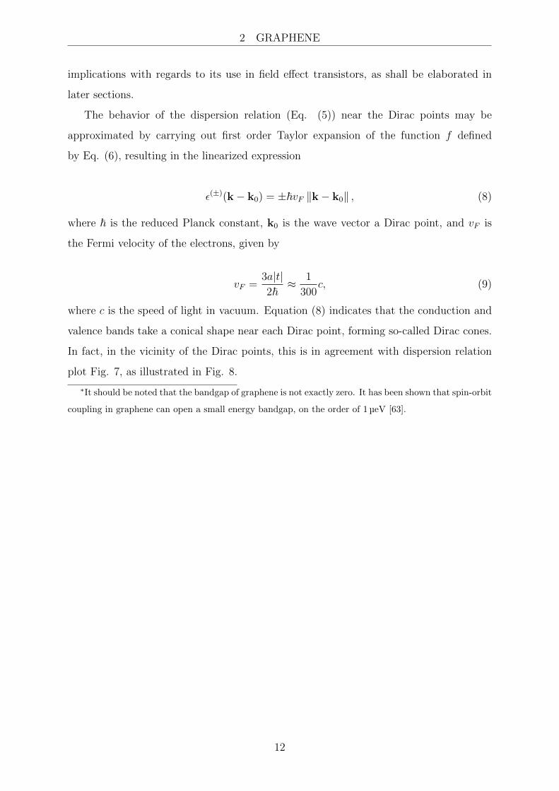
The behavior of the dispersion relation (Eq. (5)) near the Dirac points may be
approximated by carrying out first order Taylor expansion of the function f defined
by Eq. (6), resulting in the linearized expression
ε(±)(k− k0) = ±~vF ‖k− k0‖ , (8)
where ~ is the reduced Planck constant, k0 is the wave vector a Dirac point, and vF is
the Fermi velocity of the electrons, given by
vF =3a|t|2~≈ 1
300c, (9)
where c is the speed of light in vacuum. Equation (8) indicates that the conduction and
valence bands take a conical shape near each Dirac point, forming so-called Dirac cones.
In fact, in the vicinity of the Dirac points, this is in agreement with dispersion relation
plot Fig. 7, as illustrated in Fig. 8.
∗It should be noted that the bandgap of graphene is not exactly zero. It has been shown that spin-orbit
coupling in graphene can open a small energy bandgap, on the order of 1 µeV [63].
12

2 GRAPHENE
Figure 9: A zoomed in version Mathematica plot of the energy dispersion relation of
graphene (Eq. (5)), shown in Fig. 7, in the vicinity of one of the Dirac points. It is
evident that the dispersion relation becomes approximately conical in the vicinity of the
Dirac points, forming Dirac cones.
Another crucial result that appears in the vicinity of the Dirac points is the relativistic
Dirac equation. In fact, by finding the first order Taylor expansion of the function f , the
matrix representation H of the Hamiltonian describing electrons near the Dirac points
may be written as [64]∗
H = ~vFσ · k′, (10)
where σ = (σx, σy) is a vector of 2× 2 Pauli matrices σx and σy given by
σx =
0 1
1 0
(11)
∗This equation, with the vector k′ ≡ k− k0, is only valid for the K points of the first Brillouin zone.
The equivalent Dirac equation for the K ′ points may be written in the same form if k′ is redefined such
that k′x → −k′x [7].
13

2 GRAPHENE
and
σy =
0 −i
i 0
, (12)
k′ ≡ k− k0, and · denotes a standard dot product (component-wise multiplication). Be-
fore we discuss the physical implication of the above, it is convenient to slightly digress to
describe the Dirac physics concluded above. Originally, the Dirac equation was proposed
as a relativistic description of spin 1/2 particles. In a general form, the equation can be
given by.
i~γµ∂µψ −mcψ = 0 (13)
where ψ is the spinor of the fermion and γ are the so called Gamma matrices. Comparing
with equation (13),equation (10) is the Dirac equation for massless relativistic fermions in
two dimensions. Thus, π electrons in graphene behave like massless relativistic particles
near the Dirac point, making graphene a miniaturized laboratory for testing models from
quantum field theory [30]. Evidently, graphene is a material of great interest not only
in the realm of condensed matter physics and electronic engineering research, but also in
high energy physics.
2.2 Physical Properties
Graphene exhibits a myriad of remarkable mechanical, optical, and thermal properties in
addition to its novel electronic properties [22]. Some of these properties include high trans-
parency (graphene only absorbs about 2.3% of visible light), high thermal conductivity
(up to
5000 W m−1 K−1), and extraordinary mechanical properties (it is simultaneously the strongest
and thinnest material ever discovered, with a tensile strength of 130 GPa, about 200 times
stronger than steel) [64, 22]. More information about these properties can be found in
[22]. Instead, the main focus of this section is on the electronic properties of graphene.
It has been reported that graphene possesses a very high intrinsic electron mobility,
ideally exceeding 2× 105 cm2 V−1 s−1 at room temperature [22, 6]. In fact, recently, it has
been reported that heterostructures made of WSe2, graphene and hBN exhibit mobilities
as high as 3.5× 105 cm2 V−1 s−1 [14]. Graphene is capable of carrying large currents, with
an electrical conductivity higher than that of silver and zinc [22]. The high mobility of
14
2 GRAPHENE
graphene is in large part due to Eq. (10) which implies that electron backscattering is
suppressed [64]. Another explanation for the high mobility of graphene is that it exhibits
weak acoustic electron-phonon interactions [22].
Graphene has a density of states g = g(ε) given by
g(ε) =8π|ε|h2vF
, (14)
where ε is the energy, h is the Planck constant, and vF is the Fermi velocity defined in
Eq. (9) [46]. Therefore, the density of states of graphene is zero at the Dirac points.
However, graphene possesses a minimum conductivity, σ0, on the order of 4e2/h, where
e is the elementary charge and h is the Planck constant [46]. This is in accordance
with the experimentally observed anomalous quantum Hall effect in graphene – the Hall
conductivity, σxy, of graphene was found to be related to the Landau level N ∈ Z and
the minimum conductivity σ0 [46, 44] by
σxy =4Ne2
h+
1
2σ0. (15)
Although the mobility of suspended graphene can exceed 2× 105 cm2 V−1 s−1 in ideal
cases, there seems to be some variability in observed mobilities in graphene samples; for
example, mobilities ranging from 1× 103 cm2 V−1 s−1 to 7× 104 cm2 V−1 s−1 for graphene
over SiO2 [64, 6]. This is because mobility can be limited by temperature, defects, and
substrate-induced corrugations [64, 22]. Thus, different synthesis techniques result in
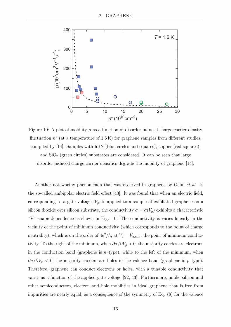
graphene samples with different mobilities. Figure 9 shows how mobilities observed in
different graphene samples vary as a function of charge carrier density fluctuation induced
by disorder in each sample [14].
15
2 GRAPHENE
Figure 10: A plot of mobility µ as a function of disorder-induced charge carrier density
fluctuation n∗ (at a temperature of 1.6 K) for graphene samples from different studies,
compiled by [14]. Samples with hBN (blue circles and squares), copper (red squares),
and SiO2 (green circles) substrates are considered. It can be seen that large
disorder-induced charge carrier densities degrade the mobility of graphene [14].
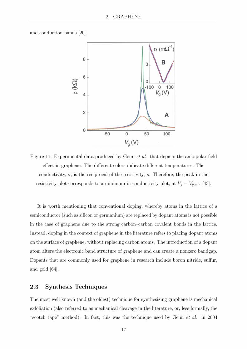
Another noteworthy phenomenon that was observed in graphene by Geim et al. is
the so-called ambipolar electric field effect [43]. It was found that when an electric field,
corresponding to a gate voltage, Vg, is applied to a sample of exfoliated graphene on a
silicon dioxide over silicon substrate, the conductivity σ = σ(Vg) exhibits a characteristic
“V” shape dependence as shown in Fig. 10. The conductivity is varies linearly in the
vicinity of the point of minimum conductivity (which corresponds to the point of charge
neutrality), which is on the order of 4e2/h, at Vg = Vg,min, the point of minimum conduc-
tivity. To the right of the minimum, when ∂σ/∂Vg > 0, the majority carries are electrons
in the conduction band (graphene is n–type), while to the left of the minimum, when
∂σ/∂Vg < 0, the majority carriers are holes in the valence band (graphene is p–type).
Therefore, graphene can conduct electrons or holes, with a tunable conductivity that
varies as a function of the applied gate voltage [22, 43]. Furthermore, unlike silicon and
other semiconductors, electron and hole mobilities in ideal graphene that is free from
impurities are nearly equal, as a consequence of the symmetry of Eq. (8) for the valence
16
2 GRAPHENE
and conduction bands [20].
Figure 11: Experimental data produced by Geim et al. that depicts the ambipolar field
effect in graphene. The different colors indicate different temperatures. The
conductivity, σ, is the reciprocal of the resistivity, ρ. Therefore, the peak in the
resistivity plot corresponds to a minimum in conductivity plot, at Vg = Vg,min [43].
It is worth mentioning that conventional doping, whereby atoms in the lattice of a
semiconductor (such as silicon or germanium) are replaced by dopant atoms is not possible
in the case of graphene due to the strong carbon–carbon covalent bonds in the lattice.
Instead, doping in the context of graphene in the literature refers to placing dopant atoms
on the surface of graphene, without replacing carbon atoms. The introduction of a dopant
atom alters the electronic band structure of graphene and can create a nonzero bandgap.
Dopants that are commonly used for graphene in research include boron nitride, sulfur,
and gold [64].
2.3 Synthesis Techniques
The most well known (and the oldest) technique for synthesizing graphene is mechanical
exfoliation (also referred to as mechanical cleavage in the literature, or, less formally, the
“scotch tape” method). In fact, this was the technique used by Geim et al. in 2004
17
2 GRAPHENE
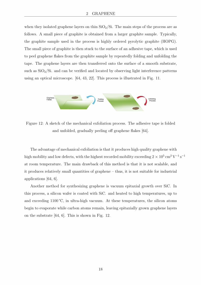
when they isolated graphene layers on thin SiO2/Si. The main steps of the process are as
follows. A small piece of graphite is obtained from a larger graphite sample. Typically,
the graphite sample used in the process is highly ordered pyrolytic graphite (HOPG).
The small piece of graphite is then stuck to the surface of an adhesive tape, which is used
to peel graphene flakes from the graphite sample by repeatedly folding and unfolding the
tape. The graphene layers are then transferred onto the surface of a smooth substrate,
such as SiO2/Si. and can be verified and located by observing light interference patterns
using an optical microscope. [64, 43, 22]. This process is illustrated in Fig. 11.
Figure 12: A sketch of the mechanical exfoliation process. The adhesive tape is folded
and unfolded, gradually peeling off graphene flakes [64].
The advantage of mechanical exfoliation is that it produces high quality graphene with
high mobility and low defects, with the highest recorded mobility exceeding 2× 105 cm2 V−1 s−1
at room temperature. The main drawback of this method is that it is not scalable, and
it produces relatively small quantities of graphene – thus, it is not suitable for industrial
applications [64, 6].
Another method for synthesizing graphene is vacuum epitaxial growth over SiC. In
this process, a silicon wafer is coated with SiC. and heated to high temperatures, up to
and exceeding 1100 °C, in ultra-high vacuum. At these temperatures, the silicon atoms
begin to evaporate while carbon atoms remain, leaving epitaxially grown graphene layers
on the substrate [64, 6]. This is shown in Fig. 12.
18

2 GRAPHENE
Figure 13: An illustration showing the main steps of epitaxial growth over SiC. The
high temperature, exceeding, 1100 °C causes silicon to sublime [26].
This technique can produce graphene samples with a mobility of up to 5× 103 cm2 V−1 s−1
at room temperature. It has also been shown that a mobility exceeding 1.1× 104 cm2 V−1 s−1
can be achieved after eliminating dangling silicon bonds from the sample. Epitaxy in-
evitably results in lower mobility and higher structural defects than mechanically cleavage
due to the burning of carbon at high temperatures, which leads to the sample being con-
taminated by hydrogen and oxygen atoms. However, the technique offers more scalability
than mechanical exfoliation [64, 6].
The most commonly used technique in industry for synthesizing graphene is chemical
vapor deposition (CVD). This technique involves mixing hydrogen and a gaseous source
of carbon such as CH4 or C2H2 over a catalytic bed made of copper or nickel in a chamber.
At high temperatures (in excess of 1000 °C), the catalyst breaks the bonds in the gaseous
sources and the hydrogen is burned, leaving graphene deposits on the surface of the
catalytic bed. This process is illustrated in Fig. 13 [64, 6].
19

2 GRAPHENE
Figure 14: An illustration of how graphene is grown using CVD. The carbon–hydrogen
bonds in CH4 are broken at high temperatures over the catalytic bed, and the hydrogen
burns and evaporates, leaving graphene deposits on the surface of the bed [64].
A larger graphene yield can be produced by using a larger catalytic bed. This makes
CVD more scalable than other graphene synthesis techniques. In addition, the cost of
CVD is lower than that of vacuum epitaxial growth and mechanical exfoliation. This
makes CVD more suitable than other techniques in industry. The disadvantage of using
CVD for graphene synthesis is the presence of point defects, grain boundaries, and surface
contaminants in the yield, all of which typically result in lower mobilities than graphene
sample produced via epitaxy or exfoliation [64, 6]. However, recently, it was reported that
with appropriate cleaning and encapsulation, the room temperature mobility of CVD
grown graphene can exceed 7× 104 cm2 V−1 s−1, which is higher than room temperature
mobilities observed in epitaxially grown graphene samples [15].
2.4 Related Structures and Bandgap Engineering
The model of graphene presented thus far is a two dimensional single layer of carbon
atoms in a honeycomb lattice of infinite spatial extent. Before discussing graphene FETs,
it is important to explore other structures that are related to the model of graphene
discussed in sections 2.1–2.3. The zero bandgap of graphene is undesirable in the context
of digital electronics, as shall be elaborated in section 3. Thus, “opening up” the bandgap
of graphene and tuning it is highly desirable for developing graphene FETs. It was
previously stated that adding dopants to graphene can result in a nonzero bandgap.
However, bandgaps generated via doping are generally not easily tunable [64]. Evidently,
bandgap engineering in graphene is crucial, and is an active ongoing area of research.
20
2 GRAPHENE
The structures presented in this section offer alternative means of generating bandgaps
in graphene. There is, however, a tradeoff – as these structures exhibit lower mobilities
than monolayer graphene.
2.4.1 Bilayer Graphene
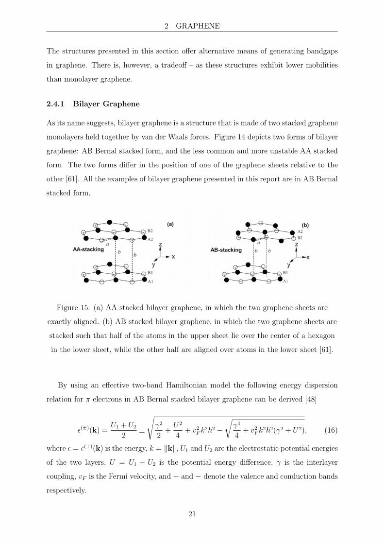
As its name suggests, bilayer graphene is a structure that is made of two stacked graphene
monolayers held together by van der Waals forces. Figure 14 depicts two forms of bilayer
graphene: AB Bernal stacked form, and the less common and more unstable AA stacked
form. The two forms differ in the position of one of the graphene sheets relative to the
other [61]. All the examples of bilayer graphene presented in this report are in AB Bernal
stacked form.
Figure 15: (a) AA stacked bilayer graphene, in which the two graphene sheets are
exactly aligned. (b) AB stacked bilayer graphene, in which the two graphene sheets are
stacked such that half of the atoms in the upper sheet lie over the center of a hexagon
in the lower sheet, while the other half are aligned over atoms in the lower sheet [61].
By using an effective two-band Hamiltonian model the following energy dispersion
relation for π electrons in AB Bernal stacked bilayer graphene can be derived [48]
ε(±)(k) =U1 + U2
2±
√γ2
2+U2
4+ v2Fk
2~2 −√γ4
4+ v2Fk
2~2(γ2 + U2), (16)
where ε = ε(±)(k) is the energy, k = ‖k‖, U1 and U2 are the electrostatic potential energies
of the two layers, U = U1 − U2 is the potential energy difference, γ is the interlayer
coupling, vF is the Fermi velocity, and + and − denote the valence and conduction bands
respectively.
21
2 GRAPHENE
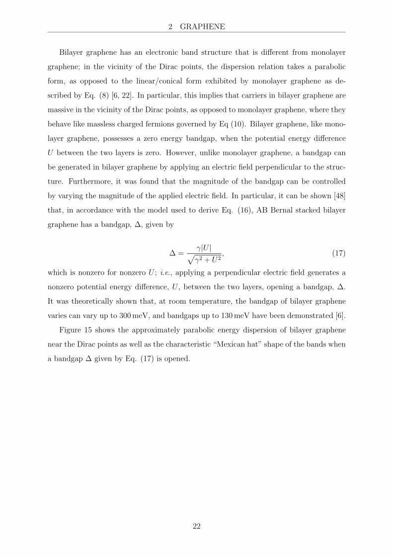
Bilayer graphene has an electronic band structure that is different from monolayer
graphene; in the vicinity of the Dirac points, the dispersion relation takes a parabolic
form, as opposed to the linear/conical form exhibited by monolayer graphene as de-
scribed by Eq. (8) [6, 22]. In particular, this implies that carriers in bilayer graphene are
massive in the vicinity of the Dirac points, as opposed to monolayer graphene, where they
behave like massless charged fermions governed by Eq (10). Bilayer graphene, like mono-
layer graphene, possesses a zero energy bandgap, when the potential energy difference
U between the two layers is zero. However, unlike monolayer graphene, a bandgap can
be generated in bilayer graphene by applying an electric field perpendicular to the struc-
ture. Furthermore, it was found that the magnitude of the bandgap can be controlled
by varying the magnitude of the applied electric field. In particular, it can be shown [48]
that, in accordance with the model used to derive Eq. (16), AB Bernal stacked bilayer
graphene has a bandgap, ∆, given by
∆ =γ|U |√γ2 + U2
, (17)
which is nonzero for nonzero U ; i.e., applying a perpendicular electric field generates a
nonzero potential energy difference, U , between the two layers, opening a bandgap, ∆.
It was theoretically shown that, at room temperature, the bandgap of bilayer graphene
varies can vary up to 300 meV, and bandgaps up to 130 meV have been demonstrated [6].
Figure 15 shows the approximately parabolic energy dispersion of bilayer graphene
near the Dirac points as well as the characteristic “Mexican hat” shape of the bands when
a bandgap ∆ given by Eq. (17) is opened.
22

2 GRAPHENE
Figure 16: A plot of the energy dispersion relation in the vicinity of a Dirac point for
AB stacked bilayer graphene in the absence (left) and the presence (right) of an applied
perpendicular electric field of magnitude E. In this diagram, the bandgap is denoted by
Eg; whereas in the main text it is denoted by ∆. The dispersion relation is
approximately parabolic in the absence of an applied electric field, and shows a
characteristic characteristic “Mexican hat” shape when a bandgap is opened via the
application of a perpendicular electric field [22].
Another way of generating a bandgap in bilayer graphene is via doping – although,
as previously stated, bandgaps generated by doping are less tunable [64]. In addition to
providing a means of bandgap engineering, bilayer grahene shows low current leakage,
which is desirable for graphene FET applications [47]. However, these advantages come
at the expense of lower carrier mobilities than in monolayer graphene, as theoretically
predicted by Wallace [60].
2.4.2 Graphene Nanoribbons
A graphene nanoribbon (GNR) is a terminated monolayer graphene sheet of small trans-
verse width on the order of 50 nm or less, much smaller than its longitudinal length
[22, 39]. π electrons in GNRs are also governed by Eq. (10), with different boundary
conditions that depend on the edges and geometry of the GNR structure. In particular,
the boundary conditions of the Dirac equation can lead to either conducting or semicon-
ducting behavior [64]. There are two variants of GNRs - those with so-called “armchair”
edges and those with “zigzag” edges, as illustrated in Fig. 16. In particular, zigzag GNRs
23
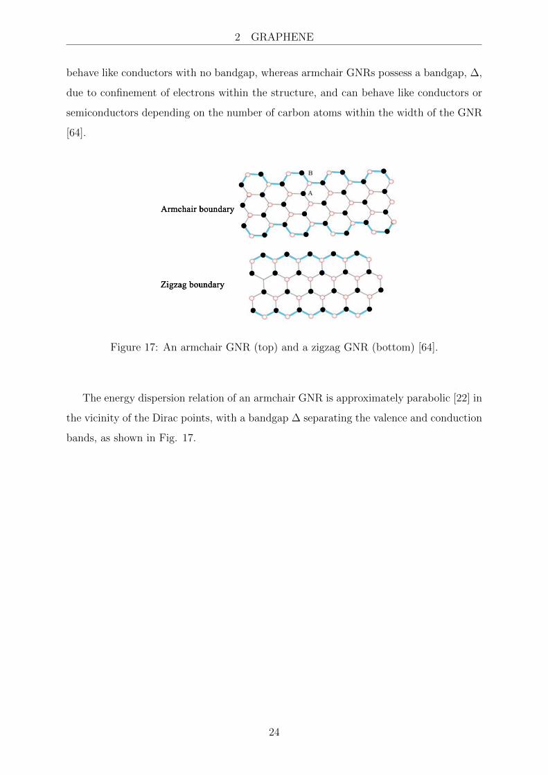
2 GRAPHENE
behave like conductors with no bandgap, whereas armchair GNRs possess a bandgap, ∆,
due to confinement of electrons within the structure, and can behave like conductors or
semiconductors depending on the number of carbon atoms within the width of the GNR
[64].
Figure 17: An armchair GNR (top) and a zigzag GNR (bottom) [64].
The energy dispersion relation of an armchair GNR is approximately parabolic [22] in
the vicinity of the Dirac points, with a bandgap ∆ separating the valence and conduction
bands, as shown in Fig. 17.
24
2 GRAPHENE
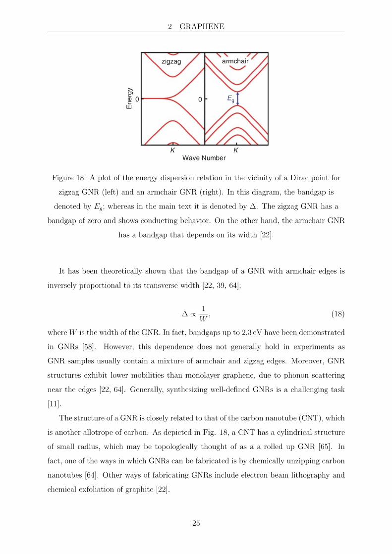
Figure 18: A plot of the energy dispersion relation in the vicinity of a Dirac point for
zigzag GNR (left) and an armchair GNR (right). In this diagram, the bandgap is
denoted by Eg; whereas in the main text it is denoted by ∆. The zigzag GNR has a
bandgap of zero and shows conducting behavior. On the other hand, the armchair GNR
has a bandgap that depends on its width [22].
It has been theoretically shown that the bandgap of a GNR with armchair edges is
inversely proportional to its transverse width [22, 39, 64];
∆ ∝ 1
W, (18)
where W is the width of the GNR. In fact, bandgaps up to 2.3 eV have been demonstrated
in GNRs [58]. However, this dependence does not generally hold in experiments as
GNR samples usually contain a mixture of armchair and zigzag edges. Moreover, GNR
structures exhibit lower mobilities than monolayer graphene, due to phonon scattering
near the edges [22, 64]. Generally, synthesizing well-defined GNRs is a challenging task
[11].
The structure of a GNR is closely related to that of the carbon nanotube (CNT), which
is another allotrope of carbon. As depicted in Fig. 18, a CNT has a cylindrical structure
of small radius, which may be topologically thought of as a a rolled up GNR [65]. In
fact, one of the ways in which GNRs can be fabricated is by chemically unzipping carbon
nanotubes [64]. Other ways of fabricating GNRs include electron beam lithography and
chemical exfoliation of graphite [22].
25

2 GRAPHENE
Figure 19: (a) An illustration of a GNR. (b) An illustration of a single-walled carbon
nanotube (SWCNT). Evidently, the CNT can be thought of as a rolled up GNR [65].
26

3 CONVENTIONAL CMOS TECHNOLOGY
3 Conventional CMOS Technology
MOSFETs have a number of advantages when compared to BJTs, including smaller size
and lower power consumption [53]. As shall be explained in this section, the MOSFET
serves two functions: it can be used as a switch or as an amplifier. The former is used
to realize logic gates and digital electronics, while the latter is used to realize analog
electronics. MOSFETs of different types can be combined on a single chip to form what
is called complementary metal oxide semiconductor (CMOS) technology, which is the
chief way in which logic gates and logic operations are implemented in modern integrated
circuits (ICs) [42].
A MOSFET is a semiconducting device with three terminals called the gate, source,
and drain [53]. This section only describes n–channel MOSFETs, but the principles of
operation of a p–channel MOSFETs are the same. The cross section of an n–channel
MOSFET and its associated circuit schematic are shown in Fig. 19 and Fig. 20, respec-
tively.∗
∗Note that in diagrams adopted from electrical engineering textbooks (such as [53]), the convention
of using lower case letters to denote circuit variables is used. This is avoided in the main text, so as
not to confuse the current variable i with the imaginary unit i =√−1 Thus, voltages and currents are
denoted by upper case letters in this report.
27

3 CONVENTIONAL CMOS TECHNOLOGY
Figure 20: Cross-sectional schematic of an n–channel MOSFET. In this particular
setup, the source (S) and drain (D) terminals are grounded. This is not a general
requirement [53].
Figure 21: Circuit symbol for an n–channel MOSFET, showing the gate (G), drain (D),
and source (S) terminals [53].
The body of the MOSFET, called the substrate, is a p–doped silicon wafer. Two
regions on the subtrate are heavily n–doped. These regions are referred to as the drain
and source regions. On top of the substrate is thin layer of silicon dioxide dielectric of
thickness tox on the order of a few nanometers, covering the region between the source
28

3 CONVENTIONAL CMOS TECHNOLOGY
and the drain. Metal contacts are deposited on the source and drain regions, and a layer
of metal or polysilicon is added on top of the oxide layer, forming what is called the gate
electrode. This defines the source, drain, and gate terminals of the device. The region
between the source and the drain is called the channel region, and has length, L, and
width, W . The channel length n most MOSFETs is on the order of tens of nanometers,
while the width is typically in the range of 0.2 µm to 100 µm [53, 42].
Suppose that the substrate, source, and gate terminals are grounded. Then, ideally,
to back-to-back p–n junctions are formed between the drain and the source, and no
current flows when a voltage VDS is applied to the drain. This is called the cutoff region
of the MOSFET. When a voltage VGS > 0 is applied to the gate, the holes in the p–
doped substrate are repelled, forming a depletion region beneath the gate, source, and
drain terminals, as shown in Fig. 19. Furthermore, majority carrier electrons from the
heavily doped n–type drain and source regions are attracted to the region underneath
the gate, forming an n–channel, or an inversion layer. The voltage at which sufficient
mobile electrons form in the n–channel is referred to as the threshold voltage, VTH . When
VGS > VTH , the MOSFET is switched on, and applying a voltage VDS > 0 causes a current
to flow from the source to the drain [53, 42].
When the voltage VDS is less than the so-called overdrive voltage VOV ≡ VGS > VTH ,
the MOSFET is said to be in the triode region, and the drain-source current IDS takes
the form
IDS = µnCoxW
L
(VOV VDS −
1
2V 2DS
), (19)
where µn is the electron mobility in the n–channel and Cox is the capacitance of the
silicon dioxide dielectric [53]. For low values of VDS, the relationship between IDS and
VDS in the triode region is approximately linear. When VDS exceeds VOV , the channel
pinchoff occurs, and the MOSFET enters the saturation region, in which the current IDS
takes the form
IDS =1
2µnCox
W
LV 2OV . (20)
Due to channel pinchoff, the drain-source current no longer depends on the voltage
VDS, and is said to be “saturated”. The full characteristic IDS–VDS dependence of an
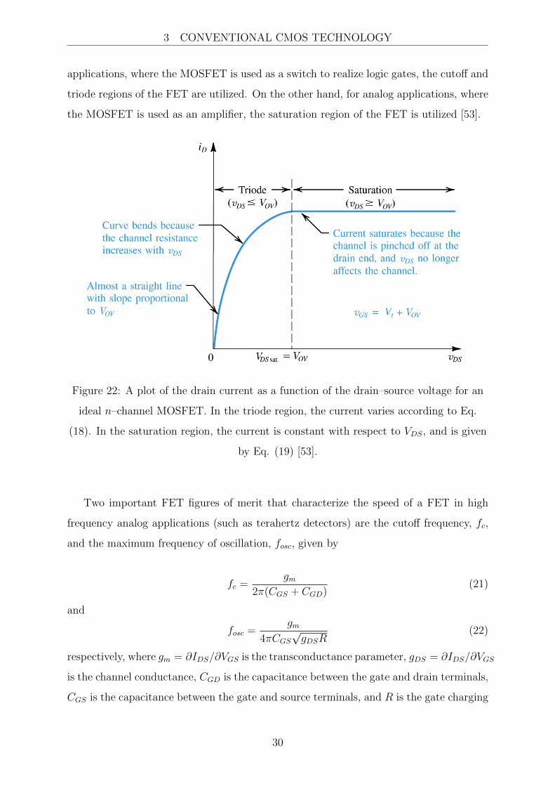
ideal MOSFET when it is turned on (VGS > VTH) is illustrated in Fig. 21. For digital
29
3 CONVENTIONAL CMOS TECHNOLOGY
applications, where the MOSFET is used as a switch to realize logic gates, the cutoff and
triode regions of the FET are utilized. On the other hand, for analog applications, where
the MOSFET is used as an amplifier, the saturation region of the FET is utilized [53].
Figure 22: A plot of the drain current as a function of the drain–source voltage for an
ideal n–channel MOSFET. In the triode region, the current varies according to Eq.
(18). In the saturation region, the current is constant with respect to VDS, and is given
by Eq. (19) [53].
Two important FET figures of merit that characterize the speed of a FET in high
frequency analog applications (such as terahertz detectors) are the cutoff frequency, fc,
and the maximum frequency of oscillation, fosc, given by
fc =gm
2π(CGS + CGD)(21)
and
fosc =gm
4πCGS√gDSR
(22)
respectively, where gm = ∂IDS/∂VGS is the transconductance parameter, gDS = ∂IDS/∂VGS
is the channel conductance, CGD is the capacitance between the gate and drain terminals,
CGS is the capacitance between the gate and source terminals, and R is the gate charging
30
3 CONVENTIONAL CMOS TECHNOLOGY
resistance induced by the dielectric [53, 64, 6]. It should be noted that the transconduc-
tance parameter, gm, is proportional to the mobility of the n–channel, µn, and inversely
proportional to the channel length, L. Thus, both fc and fosc are proportional to µn/L.
For digital applications where FETs are used to realize logic gates, an important
figure of merit that measures the performance of a MOSFET is the on–to–off current
ratio, which shall be denoted by λ in this report. A large value of λ indicates high
performance and low power leakage. Low power leakage is a highly desirable property
for a FET to have; for example, in portable electronics where an importance is placed on
the battery life of a device [53, 64, 6, 22].
31
4 STATE-OF-THE-ART GRAPHENE FETS
4 State-of-the-Art Graphene FETs
There is an urgent need for post-silicon technology in industry given the saturation of
Moore’s law, and incorporating graphene based materials into existing CMOS technology
is believed to be a potential solution. Moreover, as stated in the introduction, one of the
modern challenges of RF engineering is designing modulators and detectors that work
at the untapped terahertz gap (frequencies ranging from 0.1 THz to 10 THz). Although
mobilities of other novel devices are on the order of 1× 104 cm2 V−1 s−1, which is higher
than that of conventional CMOS devices made of silicon, they are currently not suit-
able for untapped terahertz applications due to their high cost. As discussed in section
2, graphene exhibits very high mobilities that can reach up to 2× 105 cm2 V−1 s−1 in
ideal samples, making it a suitable candidate for use in FETs that are required for high
frequency electronics [6].
One of the figures of merit introduced in section 2.1 is the on–to–off current ratio,
λ. Modern digital electronics applications require a value of λ on the order of 103 to 104
[51]. A large emphasis was placed on energy bandgaps of graphene and related structures
in section 2. This is because a nonzero energy bandgap is essential for digital electronics
applications, and a large energy bandgap corresponds to a large value of γ [22, 64, 6].
This rules out the use of monolayer graphene for digital applications. It is, however,
suitable in the realm of high frequency electronics, for which a large value of λ is not a
requirement [21, 9].
In broad terms, graphene FETs can be classified into two families [6]. The first class
of graphene FET implementations involves the use of graphene as a FET channel for
carrying current. This class of graphene FETs is typically implemented in one of three
different configurations; namely the back-gated, top-gated, and dual-gated configurations
[32], as illustrated in Fig. 22. In each of these configurations, graphene is used to form
the current-carrying channel between the source and the drain. In back-gated and dual-
gated graphene FET configurations, a highly doped Si substrate is used. In back-gated
graphene FETs, the substrate acts as the back gate of the FET, whereas in dual-gated
graphene FETs, a dielectric layer is deposited on top of the graphene channel, forming a
top gate in addition to the back gate. In top-gated graphene FETs, graphene is grown
epitaxially on a SiC substrate, and a dielectric is deposited on top of the graphene channel
to form the top gate of the device. Some of the dielectrics used include SiO2, Al2O3, and
32

4 STATE-OF-THE-ART GRAPHENE FETS
HfO2.
Figure 23: Illustrations of the cross sections of (a) a bottom-gated graphene FET, (b) a
dual-gated graphene FET, and (c) A top-gated graphene FET [32].
Another class of graphene FETs, which is not discussed in this report, hinges on the
phenomenon of quantum tunneling. This section only focuses on FETs with monolayer
graphene, bilayer graphene, and GNR channels. More information on tunneling graphene
FET implementations as well as FETs with other carbon-based channels (such as CNTs,
graphene oxide, and graphene nanomeshes) can be found in [64].
4.1 Monolayer Graphene FETs
The monolayer graphene FET was first demonstrated and studied by Lemme et al. in
2007 [33], three years after the discovery of graphene and its ambipolar behavior. One
of the key applications of monolayer graphene FETs is high frequency electronics, par-
ticularly in the untapped terahertz gap [17, 59, 34]. In fact, as stated in section 3, the
figures of merit fc and fosc which determine the speed of a FET in high frequency ap-
plications are in fact proportional to the carrier mobility in the FET channel. As such,
the parameters fc and fosc (and, by extension, the mobility, µn, and channel length, L)
introduced in section 3.1 are of key interest in this context. One of the challenges, how-
33

4 STATE-OF-THE-ART GRAPHENE FETS
ever, is that although monolayer graphene exhibits high mobility, its mobility is degraded
by the dielectric and substrates used, in addition to degradation that results from the
synthesis techniques outlined in section 2.3. A short channel length is therefore desirable
for maximizing values of fc and fosc. A cross-sectional schematic of a monolayer graphene
FET is shown in Fig. 23.
Figure 24: A cross-sectional diagram of a monolayer graphene FET in the dual-gated
configuration [9].
Meric et al. reported the first instance of a high frequency measurement of a mono-
layer graphene FET in 2008, with fc = 14.7 GHz and L = 500 nm [40]. Two years
later, monolayer graphene FETs with fc = 100 GHz and L = 240 nm [36] as well as
fc = 300 GHz and L = 144 nm [35] were realized, the latter using a nanowire gate in
order to retain a large value of mobility. In 2012, a monolayer graphene FET with a
nanowire gate was demonstrated by Cheng et al. with fc = 427 GHz, which is the high-
est achieved value of fc to date, and L = 67 nm [18, 6]. This value of fc, which is currently
the state-of-the-art for graphene FETs, is comparable with that of InP and GaAs high
electron mobility transistors (HEMTs) [8, 52]. In the past few years, advancements have
been made in using monolayer graphene FETs to realize high frequency electronics. For
example, in 2017, a 400 GHz monolayer graphene FET detector with high responsitivity
was realized [59]. In the same year, Yang et al. demonstrated a monolayer graphene FET
detector capable of terahertz detection at room temperature from 330 GHz to 500 GHz
[62]. In 2018, graphene FETs and plasmons were used for resonant terahertz radiation
detection [13].
34

4 STATE-OF-THE-ART GRAPHENE FETS
Progress in increasing fosc in monolayer graphene FETs has been slower; values of fosc
for monolayer graphene FETs typically range from 30 GHz to 200 GHz, showing poorer
performance than conventional Si-based FETs [6]. This is a result of the fact that, as
can be seen from Eq. (22), a large value of fosc requires a small value of gDS, the channel
conductance. The model of a conventional MOSFET such as that presented in section 2.1
displays a IDS–VDS shown in Fig. 21, where the current enters a saturation region when
VDS > VOV . However, graphene FETs display a more peculiar characteristic, in which
increasing VDS beyond a certain value causes IDS to vary linearly exit the saturation
region, increasing the value of gDS, which leads to a smaller value of fosc [64, 6, 40].
This is a result of interband tunneling and the quasi-ballistic nature of carrier transport
within graphene [21]. There are several engineering research groups that have studied
and modeled the effects of non-ideal IDS–VDS characteristics and other phenomena such
as negative differential resistance in monolayer graphene FETs [54, 37].
4.2 Bilayer Graphene FETs
Another way to implement a graphene FET is to use a bilayer graphene channel. A
cross-sectional schematic of a bilayer graphene FET is shown in Fig. 24.
Figure 25: A cross-sectional diagram of a bilayer graphene FET in the dual-gated
configuration [48].
Although bilayer graphene typically exhibits a lower mobility than monolayer graphene,
the use of a bilayer graphene channel in FETs offers some advantages over monolayer
35

4 STATE-OF-THE-ART GRAPHENE FETS
graphene. In particular, bilayer graphene FETs have been shown to possess a larger
intrinsic voltage gain than monolayer graphene FETs [6]. Moreover, the bandgap in-
duced in bilayer graphene by applying a perpendicular electric field has been shown to
improve current saturation and the maximum frequency of oscillation, fosc [21, 56]. This
is because the existence of a nonzero bandgap in bilayer graphene (upon the application
of a perpendicular electric field) suppresses interband tunneling. Furthermore, bilayer
graphene FETs show a leakage current that is orders of magnitude lower than that of a
typical monolayer graphene FET at low temperatures [47]. Although the gap in leakage
currents between the two FET devices decreases at higher temperatures, a lower leakage
current is desirable in both analog and digital applications.
The zero bandgap of monolayer graphene implies a small value of λ (≈ 5 for top-gated
FETs) which is unsuitable for digital applications [6]. As stated in section 2, bandgaps
as large as 130 meV have been demonstrated in bilayer graphene. For bilayer graphene
FETs, this corresponds to a value of λ ≈ 102 [52]. While this is an improvement over
the values of λ observed in monolayer graphene FETs, it is not sufficient for modern
applications in digital electronics, which require a minimum value of λ on the order of
103 to 104.
4.3 Graphene Nanoribbon FETs
An alternative to using bilayer graphene as a means of achieving a larger value of λ is to
use GNR FETs. A GNR FET has a similar structure to monolayer graphene and bilayer
graphene FETs; an armchair GNR used as a current carrying channel in the FET device,
as depicted in Fig. 25.
36

4 STATE-OF-THE-ART GRAPHENE FETS
Figure 26: A diagram of a GNR FET with a single channel [10].
Bandgaps as large as 2.3 eV have been observed in armchair graphene nanoribbons
[57], which is approximately three orders of magnitude larger than the largest bandgaps
observed in bilayer graphene under the application of a perpendicular electric field [6]. In
fact, values of λ as high as 107 have been demonstrated in sub-10 nm width p–type GNR
FETs [38] – outperforming bilayer graphene FETs by five orders of magnitude. Another
advantage of GNRs is that their small transverse width allows multiple GNRs to be used
as channels on a single device. This has the benefit of increasing the drive current and
enhancing switching characteristics for high performance applications [12].
Since GNR fabrication technology is still in its infancy, much of the performance
issues observed in GNR FETs are limited by non-idealities in GNR samples. In particular,
fabricating well-defined GNRs with high precision is not an easy task, and the existence of
zigzag edges in armchair GNR samples, can degrade the performance of a GNR FET [12].
Furthermore, although p–type GNR FETs with large values of λ have been demonstrated,
digital applications also require high performance n–type GNR FETs [6]. Furthermore,
mobility degradation is one of the biggest disadvantages of GNR FETs – for large values
of λ in the range from 104 to 107, GNRs must possess sub-10 nm width, which results in
carrier mobilities lower than 1× 103 cm2 V−1 s−1 due to phonon scattering near the edges
of the GNR.
37

5 CONCLUSION AND FUTURE PERSPECTIVES
5 Conclusion and Future Perspectives
Although graphene exhibits remarkable electronic properties that make it a suitable can-
didate for replacing silicon and extending the lifetime of Moore’s law, there remains a
lot of research to be conducted around overcoming the challenges associated with re-
alizing graphene FETs in industry. Among the challenging aspects of implementing
graphene FET technology on a large scale is the trade-off between scalability and qual-
ity of graphene samples associated with different synthesis techniques. As discussed in
section 2, CVD is the most scalable and least costly technique for synthesizing graphene
layers in industry, but results in samples with relatively low mobilities; making it difficult
to harness the potential of graphene as a high-mobility alternative to silicon.
Another key trade-off that manifests itself in this research area is that of bandgap en-
gineering and how opening a bandgap in graphene by using bilayer graphene or GNRs, as
discussed in sections 2 and 4, inevitably results in FETs with much lower mobilities than
monolayer graphene FETs. The zero bandgap of graphene is problematic for electronic
applications. Evidently, bandgap engineering is crucial for digital electronics, and of the
implementations presented in this report, GNR FETs show the most promise toward that
end, with observed on–to–off current ratios reaching 107, although there remains a lot of
work to be done in enhancing the fabrication processes by which GNRs are made, and
overcoming mobility degradation in GNR samples.
It is evident, based on the state-of-the-art review presented in section 4, that the real
potential of graphene FETs in the near future lies in high frequency applications. The
highest observed value of fc to date in monolayer graphene FETs is 427 GHz, which is
comparable to that of alternative post-silicon technologies such as InP and GaAs HEMTs,
and superior to existing conventional CMOS technologies. Moreover, terahertz graphene
FET detectors, operating at frequencies ranging from 300 GHz to 400 GHz have been
demonstrated, which is very promising and indicative of the prospects of using graphene
FETs for terahertz detectors in the near future.
Although this report examined a few examples of graphene FET implementations, it is
important to note that researchers have been exploring a much wider variety of graphene
(or carbon-based) FET implementations, such as carbon nanotube FETs, graphene oxide
FETs, graphene nanomeshes, and vertical tunneling FETs. In fact, graphene is no longer
the only two dimensional material of interest to scientists and engineers. More recently,
38
5 CONCLUSION AND FUTURE PERSPECTIVES
researchers have been examining other novel two dimensional structures such as graphyne
and silicene, which may offer advantages over graphene in terms of bandgap engineering
[64]. Overall, at present, it is unclear whether graphene will ever replace silicon in modern
consumer electronics at large, for the aforementioned reasons regarding the difficulty of
bandgap engineering and the synthesis of high mobility graphene samples on a large scale.
Nevertheless, it is becoming more apparent that graphene could play an important role
in more specialized areas of modern electronic engineering, such as terahertz technology.
39

REFERENCES
References
[1] “AMD EPYC™ 7002 Series Processors.” amd.com. https://www.amd.com/en/
processors/epyc-7002-series. [Accessed: Dec. 23, 2019].
[2] “Samsung Develops Industry’s First 3rd-generation 10nm-Class DRAM for Pre-
mium Memory Applications.” samsung.com. https://news.samsung.com/global/
samsung-develops-industrys-first-3rd-generation-10nm-class-dram-for-
premium-memory-applications. [Accessed: Dec. 20, 2019].
[3] “7 nm Technology.” tsmc.com. https://www.tsmc.com/english/
dedicatedFoundry/technology/7nm.htm. [Accessed: Dec. 20, 2019].
[4] “These 3 Computing Technologies Will Beat Moore’s Law.” forbes.com.
https://www.forbes.com/sites/stephenmcbride1/2019/04/23/these-3-
computing-technologies-will-beat-moores-law. [Accessed: Jan. 2, 2020].
[5] “Transistors Could Stop Shrinking in 2021.” ieee.org. https://spectrum.ieee.
org/semiconductors/devices/transistors-could-stop-shrinking-in-2021.
[Accessed: Jan. 2, 2020].
[6] J. Tian, “Theory, Modelling and Implementation of Graphene Field-Effect Transis-
tor,” Ph.D. dissertation, School of Electronic Engineering and Computer Science,
Queen Mary University of London, London, United Kingdom, 2017.
[7] D. Vvedensky. (2019). Quantum Theory of Matter - Graphene [Lecture Notes]. Im-
perial College London.
[8] M. Andersson, “Characterization and Modelling of Graphene FETs for Terahertz
Mixers and Detectors,” Ph.D. dissertation, Department of Microtechnology and
Nanoscience, Chalmers University of Technology, Gothenburg, Sweden, 2016.
[9] J.-D. Aguirre-Morales, S. Fregonese, C. Mukherjee, W. Wei, H. Happy, C. Ma-
neux, and T. Zimmer. A large-signal monolayer graphene field-effect transistor com-
pact model for RF-circuit applications. IEEE Transactions on Electron Devices,
64(10):4302–4309, Oct. 2017.
[10] Y. Banadaki and A. Srivastava. Effect of edge roughness on static characteristics of
graphene nanoribbon field effect transistor. Electronics, 5(4):11, Mar. 2016.
40

REFERENCES
[11] Y. M. Banadaki, S. Sharifi, W. O. Craig, and H.-C. Hou. Power and delay perfor-
mance of graphene-based circuits including edge roughness effects. 2016.
[12] Y. M. Banadaki, S. Sharifi, W. O. C. III, and H.-C. Hou. Power and delay perfor-
mance of graphene-based circuits including edge roughness effects. American Journal
of Engineering Research, 118(24):244501, 2016.
[13] D. A. Bandurin, D. Svintsov, I. Gayduchenko, S. G. Xu, A. Principi, M. Moskotin,
I. Tretyakov, D. Yagodkin, S. Zhukov, T. Taniguchi, K. Watanabe, I. V. Grigorieva,
M. Polini, G. N. Goltsman, A. K. Geim, and G. Fedorov. Resonant terahertz detec-
tion using graphene plasmons. Nature Communications, 9(1), Dec. 2018.
[14] L. Banszerus, M. Schmitz, S. Engels, J. Dauber, M. Oellers, F. Haupt, K. Watanabe,
T. Taniguchi, B. Beschoten, and C. Stampfer. Ultrahigh-mobility graphene devices
from chemical vapor deposition on reusable copper. Science Advances, 1(6):e1500222,
July 2015.
[15] L. Banszerus, M. Schmitz, S. Engels, J. Dauber, M. Oellers, F. Haupt, K. Watanabe,
T. Taniguchi, B. Beschoten, and C. Stampfer. Ultrahigh-mobility graphene devices
from chemical vapor deposition on reusable copper. Science Advances, 1(6):e1500222,
July 2015.
[16] M. Bashirpour. Review on graphene fet and its application in biosensing. Interna-
tional Journal Of Bio-Inorganic Hybrid Nanomaterials, 4:5–13, 07 2015.
[17] F. Bianco, D. Perenzoni, D. Convertino, S. L. D. Bonis, D. Spirito, M. Peren-
zoni, C. Coletti, M. S. Vitiello, and A. Tredicucci. Terahertz detection by
epitaxial-graphene field-effect-transistors on silicon carbide. Applied Physics Letters,
107(13):131104, Sept. 2015.
[18] R. Cheng, J. Bai, L. Liao, H. Zhou, Y. Chen, L. Liu, Y.-C. Lin, S. Jiang, Y. Huang,
and X. Duan. High-frequency self-aligned graphene transistors with transferred gate
stacks. Proceedings of the National Academy of Sciences, 109(29):11588–11592, July
2012.
[19] M. Donnelly, D. Mao, J. Park, and G. Xu. Graphene field-effect transistors: the
road to bioelectronics. Journal of Physics D: Applied Physics, 51(49):493001, Sept.
2018.
41

REFERENCES
[20] V. E. Dorgan, M.-H. Bae, and E. Pop. Mobility and saturation velocity in graphene
on sio2. 2010.
[21] G. Fiori, D. Neumaier, B. N. Szafranek, and G. Iannaccone. Bilayer graphene tran-
sistors for analog electronics. IEEE Transactions on Electron Devices, 61(3):729–733,
Mar. 2014.
[22] M. S. Fuhrer, C. N. Lau, and A. H. MacDonald. Graphene: Materially better carbon.
MRS Bulletin, 35(4):289–295, Apr. 2010.
[23] A. K. Geim. Nobel lecture: Random walk to graphene. Reviews of Modern Physics,
83(3):851–862, Aug. 2011.
[24] L. Gherman, O. Mos,oiu, and V. Bucinschi. The 12th international scientific con-
ference elearning and software for education. eLearning and Software for Education
Conference eLSE 2016, 1:115–122, 06 2016.
[25] H. Guo, X. Wang, D.-L. Bao, H.-L. Lu, Y.-Y. Zhang, G. Li, Y.-L. Wang, S.-X. Du,
and H.-J. Gao. Fabrication of large-scale graphene/2d-germanium heterostructure
by intercalation. Chinese Physics B, 28(7):078103, July 2019.
[26] J. Hass, J. E. Millan-Otoya, P. N. First, and E. H. Conrad. Interface structure of
epitaxial graphene grown on 4h-sic(0001). Phys. Rev. B, 78:205424, Nov 2008.
[27] C. Hubbard. 100 years since albert w. hull’s contributions to powder diffraction.
Powder Diffraction, 32(1):1–1, Feb. 2017.
[28] A. Jorio. Raman spectroscopy in graphene related systems. Wiley-VCH, Weinheim,
2011.
[29] R. M. G. K, P. Deshmukh, S. S. Prabhu, and P. K. Basu. Antenna coupled graphene-
FET as ultra-sensitive room temperature broadband THz detector. AIP Advances,
8(12):125122, Dec. 2018.
[30] M. I. Katsnelson. Zitterbewegung, chirality, and minimal conductivity in graphene.
The European Physical Journal B, 51(2):157–160, May 2006.
[31] V. K. Khanna. Short-channel effects in MOSFETs. In NanoScience and Technology,
pages 73–93. Springer India, 2016.
[32] A. V. Klekachev, A. Nourbakhsh, I. Asselberghs, A. L. Stesmans, M. M. Heyns,
and S. D. Gendt. Graphene transistors and photodetectors. Interface magazine,
22(1):63–68, Jan. 2013.
42

REFERENCES
[33] M. C. Lemme, T. J. Echtermeyer, M. Baus, and H. Kurz. A graphene field-effect
device. IEEE Electron Device Letters, 28(4):282–284, Apr. 2007.
[34] R. A. Lewis. A review of terahertz detectors. Journal of Physics D: Applied Physics,
52(43):433001, Aug. 2019.
[35] L. Liao, Y.-C. Lin, M. Bao, R. Cheng, J. Bai, Y. Liu, Y. Qu, K. L. Wang, Y. Huang,
and X. Duan. High-speed graphene transistors with a self-aligned nanowire gate.
Nature, 467(7313):305–308, Sept. 2010.
[36] Y.-M. Lin, C. Dimitrakopoulos, K. A. Jenkins, D. B. Farmer, H.-Y. Chiu, A. Grill,
and P. Avouris. 100-GHz transistors from wafer-scale epitaxial graphene. Science,
327(5966):662–662, Feb. 2010.
[37] N. Lu, L. Wang, L. Li, and M. Liu. A review for compact model of graphene field-
effect transistors. Chinese Physics B, 26(3):036804, Mar. 2017.
[38] Y. Lu, B. Goldsmith, D. R. Strachan, J. H. Lim, Z. Luo, and A. T. C. Johnson. High-
on/off-ratio graphene nanoconstriction field-effect transistor. Small, 6(23):2748–
2754, Oct. 2010.
[39] A. Maffucci and G. Miano. Electrical properties of graphene for interconnect appli-
cations. Applied Sciences, 4(2):305–317, May 2014.
[40] I. Meric, N. Baklitskaya, P. Kim, and K. L. Shepard. RF performance of top-gated,
zero-bandgap graphene field-effect transistors. In 2008 IEEE International Electron
Devices Meeting. IEEE, Dec. 2008.
[41] G. Moore. No exponential is forever: but ”forever” can be delayed! [semiconductor
industry]. In 2003 IEEE International Solid-State Circuits Conference, 2003. Digest
of Technical Papers. ISSCC. IEEE.
[42] D. Neamen. An introduction to Semiconductor devices. McGraw-Hill, Boston, 2006.
[43] K. S. Novoselov. Electric field effect in atomically thin carbon films. Science,
306(5696):666–669, Oct. 2004.
[44] K. S. Novoselov, A. K. Geim, S. V. Morozov, D. Jiang, M. I. Katsnelson, I. V.
Grigorieva, S. V. Dubonos, and A. A. Firsov. Two-dimensional gas of massless dirac
fermions in graphene. Nature, 438(7065):197–200, Nov. 2005.
43
REFERENCES
[45] Y. Ohno, K. Maehashi, and K. Matsumoto. Chemical and biological sensing ap-
plications based on graphene field-effect transistors. Biosensors and Bioelectronics,
26(4):1727–1730, Dec. 2010.
[46] P. M. Ostrovsky, I. V. Gornyi, and A. D. Mirlin. Theory of anomalous quantum hall
effects in graphene. Physical Review B, 77(19), May 2008.
[47] Y. Ouyang, P. Campbell, and J. Guo. Analysis of ballistic monolayer and bilayer
graphene field-effect transistors. Applied Physics Letters, 92(6):063120, Feb. 2008.
[48] F. Pasadas and D. Jimenez. Large-signal model of the bilayer graphene field-effect
transistor targeting radio-frequency applications: Theory versus experiment. Journal
of Applied Physics, 118(24):244501, Dec. 2015.
[49] R. Saito, G. Dresselhaus, and M. S. Dresselhaus. Physical Properties of Carbon
Nanotubes. Imperial College Press, 1998.
[50] M. Scarselli, P. Castrucci, and M. D. Crescenzi. Electronic and optoelectronic
nano-devices based on carbon nanotubes. Journal of Physics: Condensed Matter,
24(31):313202, July 2012.
[51] F. Schwierz. Graphene transistors. Nature Nanotechnology, 5(7):487–496, May 2010.
[52] F. Schwierz. Graphene transistors: Status, prospects, and problems. Proceedings of
the IEEE, 101(7):1567–1584, July 2013.
[53] A. Sedra. Microelectronic Circuits. Oxford University Press, New York, 2016.
[54] P. Sharma, L. S. Bernard, A. Bazigos, A. Magrez, and A. M. Ionescu. Room-
temperature negative differential resistance in graphene field effect transistors: Ex-
periments and theory. ACS Nano, 9(1):620–625, Jan. 2015.
[55] S. Simon. The Oxford Solid State Basics. Oxford University Press, Oxford, 2013.
[56] B. N. Szafranek, G. Fiori, D. Schall, D. Neumaier, and H. Kurz. Current saturation
and voltage gain in bilayer graphene field effect transistors. Nano Letters, 12(3):1324–
1328, Feb. 2012.
[57] L. Talirz, H. Sode, S. Kawai, P. Ruffieux, E. Meyer, X. Feng, K. Mullen, R. Fasel,
C. A. Pignedoli, and D. Passerone. Band gap of atomically precise graphene nanorib-
bons as a function of ribbon length and termination. ChemPhysChem, 20(18):2348–
2353, Aug. 2019.
44

REFERENCES
[58] L. Talirz, H. Sode, S. Kawai, P. Ruffieux, E. Meyer, X. Feng, K. Mullen, R. Fasel,
C. A. Pignedoli, and D. Passerone. Band gap of atomically precise graphene nanorib-
bons as a function of ribbon length and termination. 2019.
[59] L. Vicarelli, M. S. Vitiello, D. Coquillat, A. Lombardo, A. C. Ferrari, W. Knap,
M. Polini, V. Pellegrini, and A. Tredicucci. Graphene field-effect transistors as room-
temperature terahertz detectors. Nature Materials, 11(10):865–871, Sept. 2012.
[60] P. R. Wallace. The band theory of graphite. Physical Review, 71(9):622–634, May
1947.
[61] Y. Xu, X. Li, and J. Dong. Infrared and raman spectra of AA-stacking bilayer
graphene. Nanotechnology, 21(6):065711, Jan. 2010.
[62] X. Yang, A. Vorobiev, A. Generalov, M. A. Andersson, and J. Stake. A flexible
graphene terahertz detector. Applied Physics Letters, 111(2):021102, July 2017.
[63] Y. Yao, F. Ye, X.-L. Qi, S.-C. Zhang, and Z. Fang. Spin-orbit gap of graphene:
First-principles calculations. Physical Review B, 75(4), Jan. 2007.
[64] K. C. Yung, W. M. Wu, M. P. Pierpoint, and F. V. Kusmartsev. Introduction to
graphene electronics – a new era of digital transistors and devices. 2013.
[65] W.-S. Zhao, K. Fu, D.-W. Wang, M. Li, G. Wang, and W.-Y. Yin. Mini-review:
Modeling and performance analysis of nanocarbon interconnects. Applied Sciences,
9(11):2174, May 2019.
45

APPENDIX
Appendix
In this appendix, the electronic band structure of graphene is derived using the tight
binding method. This derivation has largely been adapted from [7].
As described in section 2, a unit cell in graphene contains two atoms – each from one
of the interpenetrating sublattices. Suppose that the two sublattices are labeled by A
and B, in accordance with Fig. 4. Then, the Bloch functions associated with sublattices
A and B may be defined by
ψ(A)k (r) =
1√N
∑RA
eik·RAφA(r−RA) (A.1)
and
ψ(B)k (r) =
1√N
∑RB
eik·RBφB(r−RB) (A.2)
respectively, where N is the number of unit cells, r is a position vector, k is the wave
vector associated with crystal momentum ~k , Rα is the lattice vector associated with
a carbon atom in the sublattice α, and φα(r − Rα) is a normalized eigenstate of the
Hamiltonian of a carbon atom in the sublattice α. The trial wave function, ψk, may then
be written as
ψk(r) = akψ(A)k (r) + bkψ
(A)k (r), (A.3)
where ak, bk ∈ C are complex coefficients that depend on k. Substituting the trial wave
function into the time-independent Schrodinger equation, one obtains
Hψk = εkψk, (A.4)
where H is the Hamiltonian operator and εk is the energy eigenvalue associated with k.
Multiplying both sides of Eq. (A.4) by ψ†k and carrying out a spatial integration over the
unit cell yields
(a∗k b∗k
)Hk
a∗kb∗k
= εk
(a∗k b∗k
)Sk
a∗kb∗k
, (A.5)
where Hk is the matrix representation of the Hamiltonian operator in the(|ψ(A)
k 〉, |ψ(B)k 〉
)basis, namely,
46
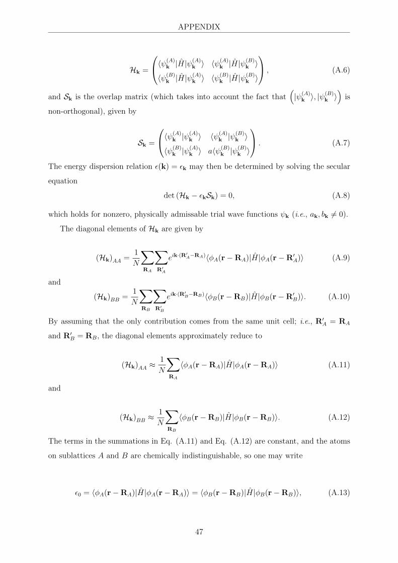
APPENDIX
Hk =
〈ψ(A)k |H|ψ
(A)k 〉 〈ψ
(A)k |H|ψ
(B)k 〉
〈ψ(B)k |H|ψ
(A)k 〉 〈ψ
(B)k |H|ψ
(B)k 〉
, (A.6)
and Sk is the overlap matrix (which takes into account the fact that(|ψ(A)
k 〉, |ψ(B)k 〉
)is
non-orthogonal), given by
Sk =
〈ψ(A)k |ψ
(A)k 〉 〈ψ(A)
k |ψ(B)k 〉
〈ψ(B)k |ψ
(A)k 〉 a〈ψ(B)
k |ψ(B)k 〉
. (A.7)
The energy dispersion relation ε(k) = εk may then be determined by solving the secular
equation
det (Hk − εkSk) = 0, (A.8)
which holds for nonzero, physically admissable trial wave functions ψk (i.e., ak, bk 6= 0).
The diagonal elements of Hk are given by
(Hk)AA =1
N
∑RA
∑R′
A
eik·(R′A−RA)〈φA(r−RA)|H|φA(r−R′A)〉 (A.9)
and
(Hk)BB =1
N
∑RB
∑R′
B
eik·(R′B−RB)〈φB(r−RB)|H|φB(r−R′B)〉. (A.10)
By assuming that the only contribution comes from the same unit cell; i.e., R′A = RA
and R′B = RB, the diagonal elements approximately reduce to
(Hk)AA ≈1
N
∑RA
〈φA(r−RA)|H|φA(r−RA)〉 (A.11)
and
(Hk)BB ≈1
N
∑RB
〈φB(r−RB)|H|φB(r−RB)〉. (A.12)
The terms in the summations in Eq. (A.11) and Eq. (A.12) are constant, and the atoms
on sublattices A and B are chemically indistinguishable, so one may write
ε0 = 〈φA(r−RA)|H|φA(r−RA)〉 = 〈φB(r−RB)|H|φB(r−RB)〉, (A.13)
47

APPENDIX
where ε0 is an energy parameter associated with the atomic eigenstates φA and φB. It
follows that the diagonal elements of the Hamiltonian matrix reduce to
(Hk)AA = (Hk)BB = ε0, (A.14)
by noting that the sums in Eq. (A.11) and Eq. (A.12) are sums over N unit cells. The
diagonal elements of Sk are given by
(Sk)AA =1
N
∑RA
∑R′
A
eik·(R′A−RA)〈φA(r−RA)|φA(r−R′A)〉 (A.15)
and
(Sk)BB =1
N
∑RB
∑R′
B
eik·(R′B−RB)〈φB(r−RB)|φB(r−R′B)〉. (A.16)
Applying the same approximation (assuming that the dominant contribution comes from
the same unit cell), the diagonal terms approximately reduce to
(Sk)AA ≈1
N
∑RA
〈φA(r−RA)|φA(r−RA)〉 (A.17)
and
(Sk)BB ≈1
N
∑RB
〈φB(r−RB)|φB(r−RB)〉. (A.18)
Since the eigenstates φA and φB are normalized,
〈φA(r−RA)|φA(r−RA)〉 = 〈φB(r−RB)|φB(r−RB)〉 = 1, (A.19)
and, by noting that the summations in Eq. (A.17) and Eq. (A.18) are over N unit cells,
(Sk)AA = (Sk)BB = 1. (A.20)
Figure 4 shows the how the position a carbon atom in the A sublattice relative to its
three neighboring carbon atoms in the B sublattice. In particular, with respect to the
coordinate system (e1, e2, e3), the three displacement vectors v1, v2,and v3 from an A
atom to its three nearest neighbors (B atoms) may be written as
48

APPENDIX
v1 = ae2, (A.21)
v2 =1
2(a′e1 − ae2), (A.22)
and
v3 = −1
2(a′e1 + ae2), (A.23)
where a ≈ 1.42�A is the interatomic spacing between the carbon atoms and a′ = a√
3 is
the lattice constant. Considering the off-diagonal matrix element (Hk)AB
(Hk)AB =1
N
∑RA
∑RB
eik·(RB−RA)〈φA(r−RA)|H|φA(r−RB)〉, (A.24)
the inner sum may be approximated by
∑RB
eik·(RB−RA)〈φA(r−RA)|H|φA(r−RB)〉 ≈3∑j=1
eik·vj〈φA(r−RA)|H|φA(r−(RA+vj))〉
(A.25)
if the only interactions considered are the interactions between the A atom and its three
nearest neighbors. Therefore, Eq. (A.24) may be rewritten as
(Hk)AB =1
N
3∑j=1
∑RA
eik·vj〈φA(r−RA)|H|φA(r− (RA + vj))〉. (A.26)
By noting that 〈φA(r−RA)|H|φA(r− (RA + vj))〉 is a constant term in the summation,
one may write
t = 〈φA(r−RA)|H|φA(r− (RA + vj))〉, (A.27)
where t ∈ R is a tight binding hopping parameter. Therefore,
(Hk)AB = t
3∑j=1
eik·vj = t h(k) (A.28)
where h is a complex-valued function of k defined by
49
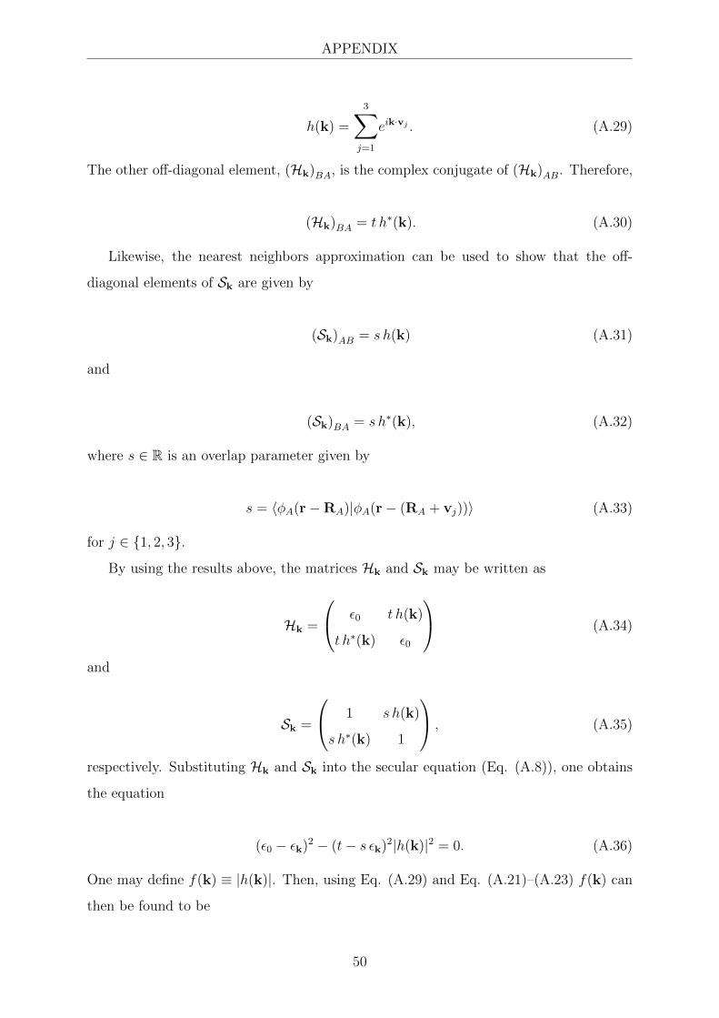
APPENDIX
h(k) =
3∑j=1
eik·vj . (A.29)
The other off-diagonal element, (Hk)BA, is the complex conjugate of (Hk)AB. Therefore,
(Hk)BA = t h∗(k). (A.30)
Likewise, the nearest neighbors approximation can be used to show that the off-
diagonal elements of Sk are given by
(Sk)AB = s h(k) (A.31)
and
(Sk)BA = s h∗(k), (A.32)
where s ∈ R is an overlap parameter given by
s = 〈φA(r−RA)|φA(r− (RA + vj))〉 (A.33)
for j ∈ {1, 2, 3}.
By using the results above, the matrices Hk and Sk may be written as
Hk =
ε0 t h(k)
t h∗(k) ε0
(A.34)
and
Sk =
1 s h(k)
s h∗(k) 1
, (A.35)
respectively. Substituting Hk and Sk into the secular equation (Eq. (A.8)), one obtains
the equation
(ε0 − εk)2 − (t− s εk)2|h(k)|2 = 0. (A.36)
One may define f(k) ≡ |h(k)|. Then, using Eq. (A.29) and Eq. (A.21)–(A.23) f(k) can
then be found to be
50

APPENDIX
f(k) =
√√√√1 + 4 cos
(3kya
2
)cos
(√3kxa
2
)+ 4 cos2
(√3kxa
2
). (A.37)
Finally, solving for ε(k) = εk in Eq. (A.36) gives the dispersion relation
ε(±)(k) =ε0 ± t f(k)
1± s f(k), (A.38)
where + denotes the conduction band while − denotes the valence band.
51