impact of silicon nitride thickness on the infrared sensitivity of silicon ...
29
IMPACT OF SILICON NITRIDE THICKNESS ON THE INFRARED SENSITIVITY OF SILICON NITRIDE-ALUMINUM MICROCANTILEVERS BY MATTHEW R. ROSENBERGER THESIS Submitted in partial fulfillment of the requirements for the degree of Master of Science in Mechanical Engineering in the Graduate College of the University of Illinois at Urbana-Champaign, 2012 Urbana, Illinois Adviser: Professor William Paul King
Transcript of impact of silicon nitride thickness on the infrared sensitivity of silicon ...
IMPACT OF SILICON NITRIDE THICKNESS ON THE INFRARED SENSITIVITY OF SILICON NITRIDE-ALUMINUM MICROCANTILEVERS
BY
MATTHEW R. ROSENBERGER
THESIS
Submitted in partial fulfillment of the requirements for the degree of Master of Science in Mechanical Engineering
in the Graduate College of the University of Illinois at Urbana-Champaign, 2012
Urbana, Illinois
Adviser:
Professor William Paul King
II
ABSTRACT
This thesis investigates how silicon nitride thickness impacts the performance of silicon
nitride - aluminum bimaterial cantilever infrared sensors. A model predicts cantilever behavior
by considering heat transfer within and from the cantilever, cantilever optical properties,
cantilever bending mechanics, and thermomechanical noise. Silicon nitride-aluminum bimaterial
cantilevers of different thicknesses were designed and fabricated. Cantilever sensitivity and
noise were measured when exposed to infrared laser radiation. For cantilever thickness up to
1200 nm, thicker silicon nitride results in improved signal to noise ratio due to increased
absorptivity and decreased noise. The best cantilever had an incident flux sensitivity of 2.1 × 10-
3 V W-1 m2 and an incident flux signal to noise ratio of 406 Hz1/2 W-1 m2, which is more than an
order of magnitude improvement compared to the best commercial cantilever.

III
This thesis is dedicated to my Lord and Savior, Jesus Christ, and to my parents for their unending support and encouragement.
IV
ACKNOWLEDGMENTS
I would like to acknowledge my advisor, professor William Paul King, for providing me with the
opportunity to work in his research group and for his guidance. I would like to thank professor David G.
Cahill for his valuable insight. I would also like to acknowledge Beomjin Kwon for his help with the
experimental setup and for many fruitful discussions. I would like to thank my colleagues in professor
King’s group for their technical assistance and friendship. Finally, I would like to acknowledge the Air
Force Office of Scientific Research for financially supporting my work.
V
TABLE OF CONTENTS
CHAPTER 1: INTRODUCTION ................................................................................................ 1
CHAPTER 2: MODELING ......................................................................................................... 3
CHAPTER 3: CANTILEVER FABRICATION AND CHARACTERIZATION .................. 9
CHAPTER 4: RESULTS AND DISCUSSION ........................................................................ 15
CHAPTER 5: CONCLUSION................................................................................................... 21
REFERENCES ............................................................................................................................ 22
1
CHAPTER 1: INTRODUCTION
Bimaterial cantilevers are sensitive thermometers with resolutions in the range of 2 µK [1]
and 100 pW [2]. Bimaterial cantilevers are effective temperature sensors at room temperature
because their noise characteristics are not a strong function of temperature [3]. As a result, many
researchers have explored uncooled infrared (IR) imaging with bimaterial cantilevers [4-6].
Published research reports modeling and design of biomaterial cantielvers that has
resulted in substantial performance improvements. Aluminum - silicon nitride is a better
material combination than gold - silicon nitride because aluminum has a higher thermal
expansion coefficient and a similar Young’s modulus compared to gold [1]. When heat is
absorbed at the cantilever free end, the optimal thickness ratio of an aluminum - silicon nitride
cantilever is 0.26 [1]. An aluminum – silicon nitride cantilever with a thickness ratio of 0.25 had
a measured heat flow resolution of 40 pW when uniformly illuminated by incident light [3].
When a gold - silicon nitride cantilever is heated to a uniform temperature, the thickness ratio to
maximize sensitivity is 0.75 [4]. Increasing the thermal isolation of the absorbing area can
enhance cantilever sensitivity [4, 7]. Despite intense research in this general area, the effect of
total cantilever thickness [4] and optical properties [8] has been somewhat less studied.
In a metal-dielectric cantilever, the metal layer reflects incident light while the dielectric
layer absorbs incident light. The thickness of both layers affect cantilever temperature sensitivity
and noise, while the thickness of the dielectric layer affects cantilever absorption. Silicon nitride
is a common choice for the absorbing dielectric layer because it has relatively high absorption
across the relevant IR wavelength range of 8-14 µm [4]. The refractive index of silicon nitride
has a large imaginary part in this IR range [9] that results in a strong dependence of absorptivity
2
on layer thickness up to 1.5 µm, with absorptivity increasing with thickness. Cantilever noise
decreases with thickness because the cantilever becomes more rigid as thickness increases.
However, cantilever temperature sensitivity, which is independent of absorptivity, decreases with
increasing thickness [1, 4]. Previous publications have not considered this tradeoff between
cantilever absorptivity, noise, and temperature sensitivity. This work uses modeling and
experiments to investigate how silicon nitride thickness affects the performance of silicon nitride
– aluminum bimaterial cantilevers.
3
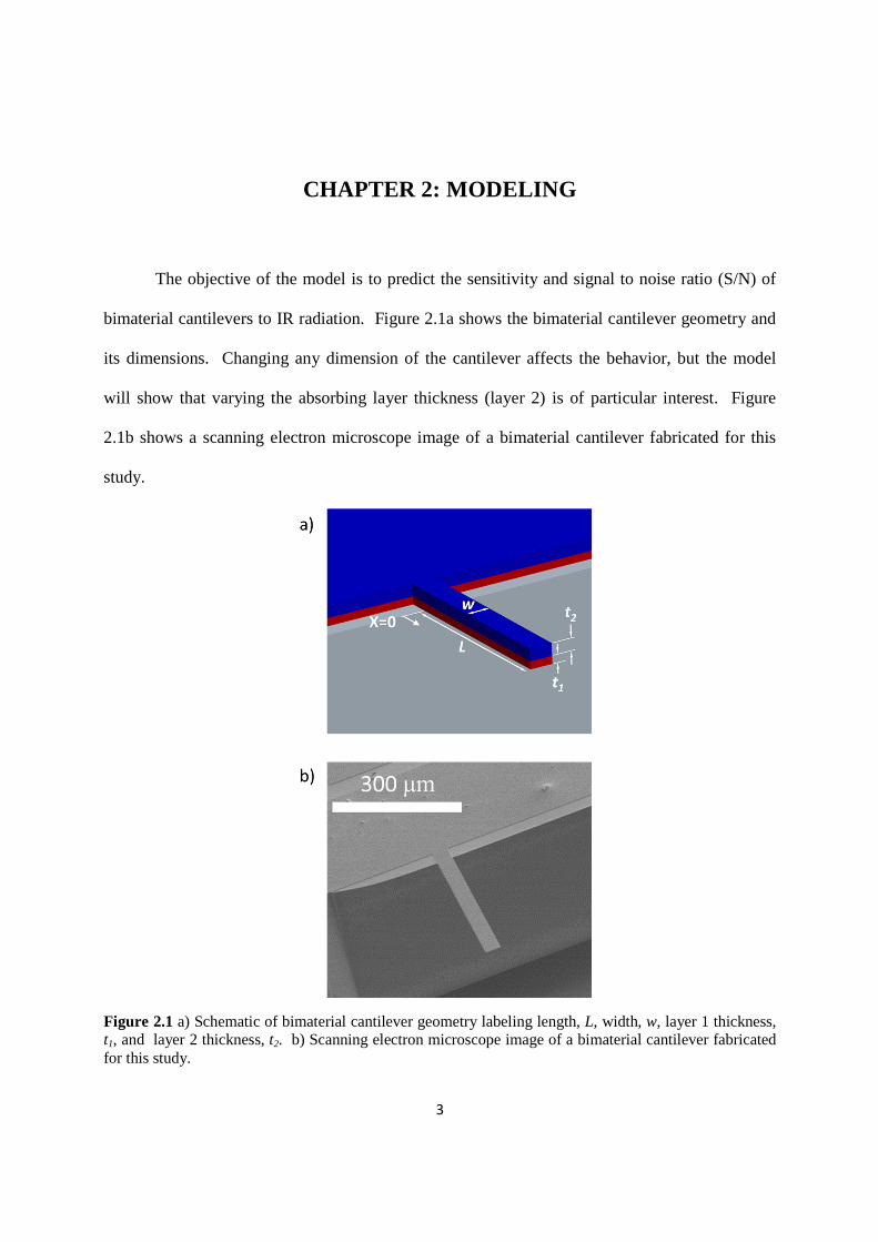
CHAPTER 2: MODELING
The objective of the model is to predict the sensitivity and signal to noise ratio (S/N) of
bimaterial cantilevers to IR radiation. Figure 2.1a shows the bimaterial cantilever geometry and
its dimensions. Changing any dimension of the cantilever affects the behavior, but the model
will show that varying the absorbing layer thickness (layer 2) is of particular interest. Figure
2.1b shows a scanning electron microscope image of a bimaterial cantilever fabricated for this
study.
Figure 2.1 a) Schematic of bimaterial cantilever geometry labeling length, L, width, w, layer 1 thickness, t1, and layer 2 thickness, t2. b) Scanning electron microscope image of a bimaterial cantilever fabricated for this study.
4
Bimaterial cantilever thermal bending can be modeled as a bimaterial strip thermostat
[10]. Equating the strain in the two materials at their interface gives the cantilever bending as
( ) ( ) ( )2
1 21 2 02 2
2
6d z x t t
T x Tdx t K
α α += − −
(1)
where
2 31 2
2 1
4 6 4E E
K r r rE E r
= + + + + , (2)
z(x) is the cantilever deflection along its length, α is the thermal expansion coefficient, t is the
layer thickness, T(x)-T0 is the temperature difference between the cantilever and the environment
temperature, r = t1/t2, E is the Young’s modulus, and the subscripts refer to the two materials.
The boundary conditions for Eq. (1) are dz/dx = 0 and z = 0 at x = 0.
The temperature distribution within the cantilever can be considered one-dimensional,
since the Biot number for a cantilever is less than 10-3 [11]. Heat flow from the cantilever to the
nearby environment can be modeled using a constant convection heat transfer coefficient, h =
1000 W/m2-K [12-15]. The incident radiation flux on the cantilever, qrad” , is uniform over the
entire cantilever. With these considerations, the steady state temperature distribution in the
cantilever is
( ) ( )( ) ( )1 21x C cosh x C sinh xθ β β= − + (3)
( )1 1 2 2
hP
w t tβ
λ λ=
+ (4)
''
1radAq w
ChP
= − (5)
5
( ) ( )
( ) ( )
''
2
1rad
sinh L cosh LAq w hChP sinh L cosh L
h
λ β β β
λβ β β
+ −=
+ (6)
where ( ) 0( )x T x Tθ = − , A is cantilever absorptivity, P is the perimeter of the cantilever cross
section, and λ is the thermal conductivity. The steady state temperature distribution is considered
because it corresponds to the largest deflection. The boundary conditions are ( )0 0θ = and
( )x L
d hL
dx
θ θλ=
= .
Cantilever tip slope determines the difference signal measured by the position sensitive
detector (PSD) in an atomic force microscope (AFM) [16]. Combining Eqs. (1) and (3), the
cantilever slope at the free end is
( ) ( ) ( )1 21 2 1 1 2 32
2
6x L
sinh L cosh Lt tdzC C x C C
dx t K
β βα α
β β=
+= − − + +
(7)
where C3 = -C2 / β. To compare modeling with experiments, we relate cantilever tip slope with
the PSD difference signal through the inverse optical lever sensitivity (InvOLS). The InvOLS is
the ratio of tip deflection to the PSD difference signal when the cantilever tip is in contact with a
surface. For this loading condition, the ratio of tip deflection to tip slope is 2L/3 [17]. Therefore,
the factor relating PSD difference signal to cantilever tip slope is 3/(2L)·InvOLS.
Cantilever absorptivity is calculated with the transfer matrix method and depends on the
thickness and refractive index of the cantilever materials [18]. The modeling is specifically for
the experimental laser wavelength, 10.35 µm, but similar trends exist for different wavelengths.
Reflectivity measurements and optical modeling show that the refractive index of our plasma
enhanced chemical vapor deposition (PECVD) silicon nitride films is (1.24±0.05) + i (1.15±0.15)
at a wavelength of 10.35 µm. The measured refractive index of our silicon nitride films is
6
similar to that found in previous studies of PECVD silicon nitride [9]. Commercial AFM
cantilevers contain low-pressure chemical vapor deposition silicon nitride which has a refractive
index of 1.28 + i1.88 at 10.35 µm [19].
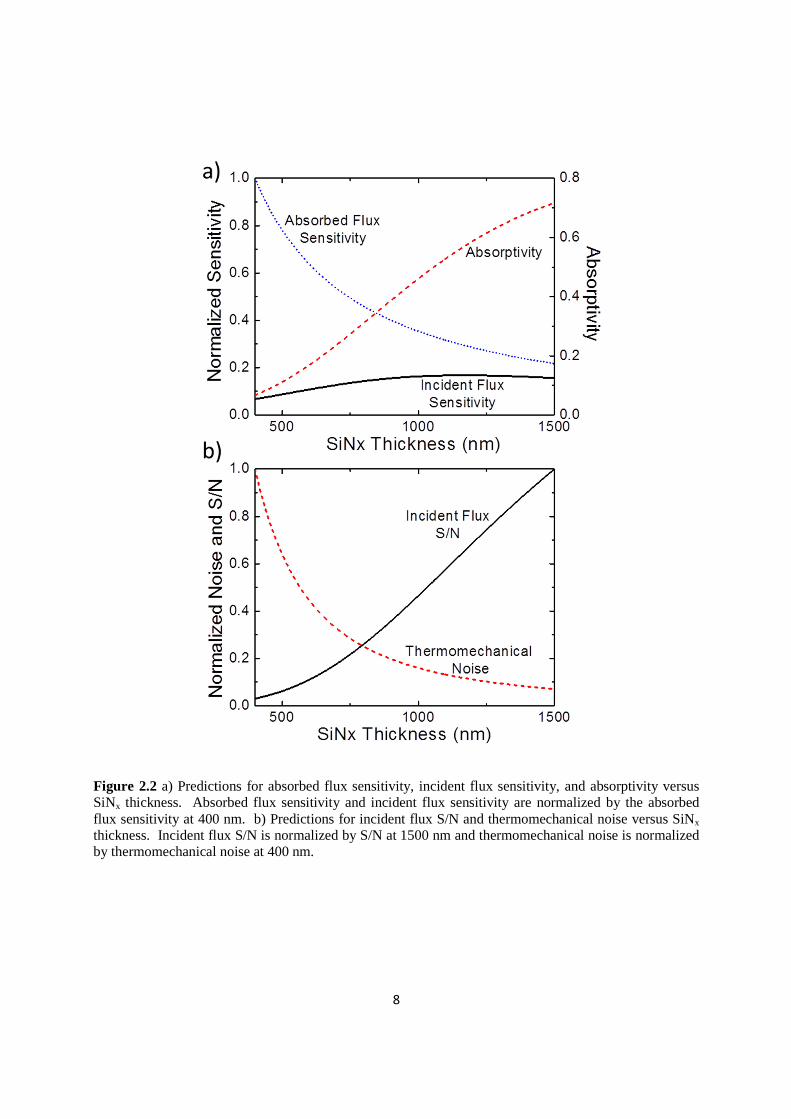
Figure 2.2a shows predictions for absorptivity, absorbed flux sensitivity (independent of
absorptivity), and incident flux sensitivity as functions of silicon nitride thickness for constant r,
L = 450 µm, and w = 40 µm. The incident flux sensitivity is the product of absorbed flux
sensitivity and absorptivity. Absorptivity changes significantly in the 400-1500 nm silicon
nitride thickness range. As cantilever thickness increases, the absorbed flux sensitivity
monotonically decreases. However, the incident flux sensitivity has a local maximum because
the steep positive slope of absorptivity overwhelms the negative slope of absorbed flux
sensitivity until around 1200 nm.
S/N determines the detection resolution of bimaterial cantilever sensors. There are many
sources of noise in cantilever sensors including temperature fluctuation noise, optical readout
noise, and thermomechanical noise [7]. Thermomechanical noise [4] is a dominant noise source
for cantilevers with an optical system for deflection measurement [20]. The frequency
distribution of noise is relevant because heat inputs to bimaterial cantilevers are often modulated
at a specific drive frequency [1, 3, 7, 15, 21, 22]. At frequencies well below mechanical
resonance, the root mean square amplitude of cantilever tip deflections from thermomechanical
noise is [23]:
1/22
0
4 BTM
k TBz
Qkδ
ω= (8)
where kB is the Boltzmann constant, B is the measurement bandwidth, Q is the quality factor, k is
the mechanical spring constant, and ω0 is the mechanical resonance frequency. The tip slope
noise is the product of Eq. (8) and the ratio of tip slope to tip deflection for the first vibrational
7
bending mode, 1.3765/L [20]. Slope is converted to signal through the InvOLS as described for
the cantilever response to radiation. While thermomechanical noise decreases with increased
stiffness, the noise floor is governed by the AFM, which in our case was 5 × 10⁻⁶ V Hz-1/2.
Figure 2.2b shows the qualitative behavior of thermomechanical noise and incident flux S/N with
respect to silicon nitride thickness. The model predicts that an increase in silicon nitride layer
thickness corresponds to an increase in S/N.
8
Figure 2.2 a) Predictions for absorbed flux sensitivity, incident flux sensitivity, and absorptivity versus SiNx thickness. Absorbed flux sensitivity and incident flux sensitivity are normalized by the absorbed flux sensitivity at 400 nm. b) Predictions for incident flux S/N and thermomechanical noise versus SiNx thickness. Incident flux S/N is normalized by S/N at 1500 nm and thermomechanical noise is normalized by thermomechanical noise at 400 nm.

9
CHAPTER 3: CANTILEVER FABRICATION AND CHARACTERIZATION
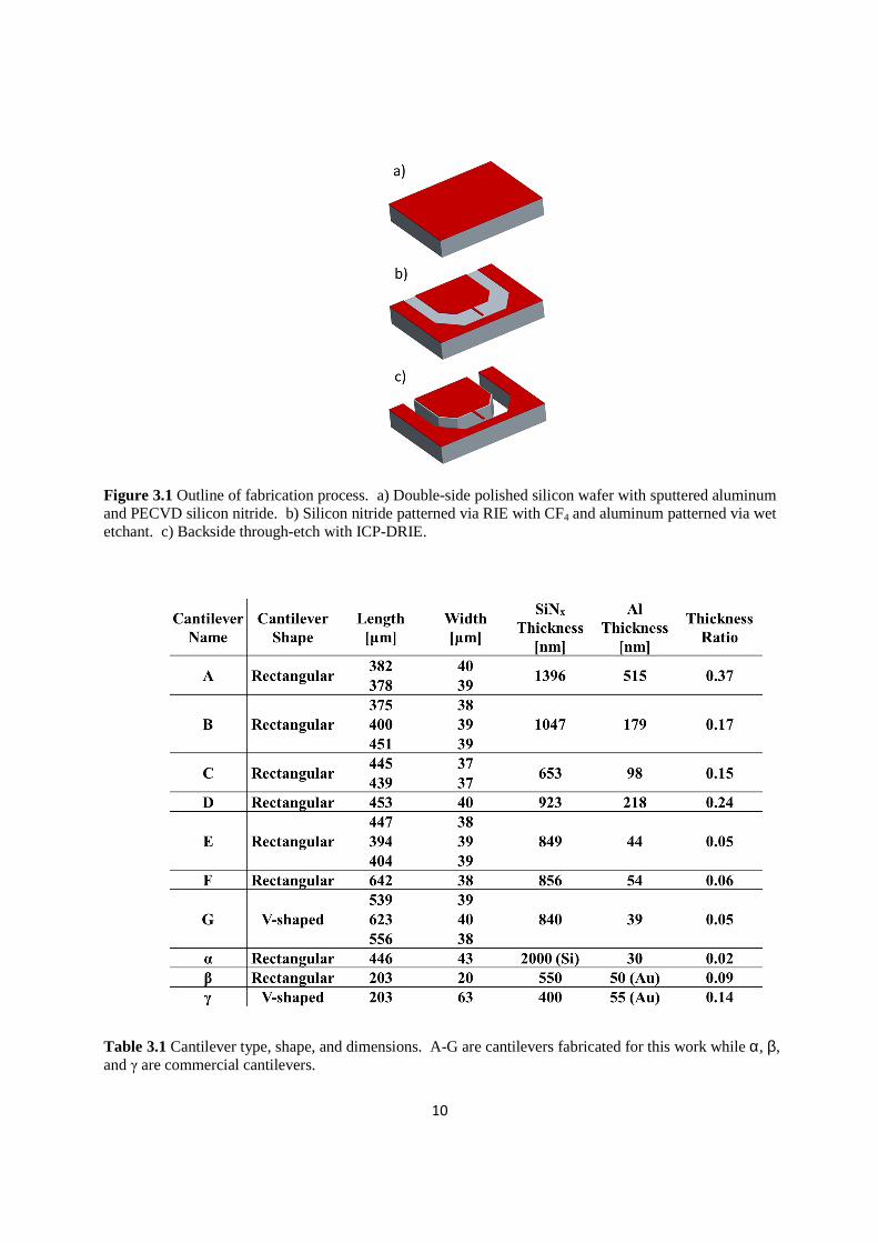
Figure 3.1 shows the fabrication process for our bimaterial cantilevers. The fabrication
process began with a 400 µm thick double side polished silicon wafer. First, an aluminum layer
was sputtered or evaporated onto the silicon surface. PECVD silicon nitride was then deposited
on top of the aluminum. To compensate for compressive thermal stress, the silicon nitride film
was deposited at high frequency which generally leads to tensile stress [24]. PECVD silicon
nitride films are not necessarily stoichiometric and so here we refer to the silicon nitride as SiNx
[9]. The films were annealed at 375 °C to improve adhesion between SiNx and aluminum and to
mitigate intrinsic stresses. The SiNx layer was patterned and plasma etched, and then the
aluminum layer was wet etched. Finally, the cantilevers were released with deep reactive ion
etching from the wafer back side. Annealing between 175 °C and 185 °C caused initially bent
cantilevers to become flat enough for use in an AFM. Figure 2.1b shows a released cantilever.
Table 3.1 shows the measured dimensions of all fabricated cantilevers as well as several
commercial cantilevers that were studied.
10
Figure 3.1 Outline of fabrication process. a) Double-side polished silicon wafer with sputtered aluminum and PECVD silicon nitride. b) Silicon nitride patterned via RIE with CF4 and aluminum patterned via wet etchant. c) Backside through-etch with ICP-DRIE.
Table 3.1 Cantilever type, shape, and dimensions. A-G are cantilevers fabricated for this work while α, β, and γ are commercial cantilevers.

11
The goal of the characterization was to measure cantilever bending sensitivity and S/N
when exposed to IR radiation. Figure 3.2 shows the experimental setup. A cantilever was
mounted in an AFM and the optical readout system in the AFM head measured the deflection.
A CO2 laser tuned to 10.35 µm illuminated the cantilever. The beam diameter from the laser was
2.4 mm. A 1 mm diameter aperture was positioned between the laser and the cantilever, and the
flux through the aperture was assumed constant because the beam diameter was considerably
larger than the aperture.
Figure 3.2 Diagram of experimental setup. The Gaussian beam from the CO2 laser is restricted by an aperture to create approximately uniform incident light at the cantilever. The AFM PSD senses deflection of the cantilever that is mounted in the AFM head.
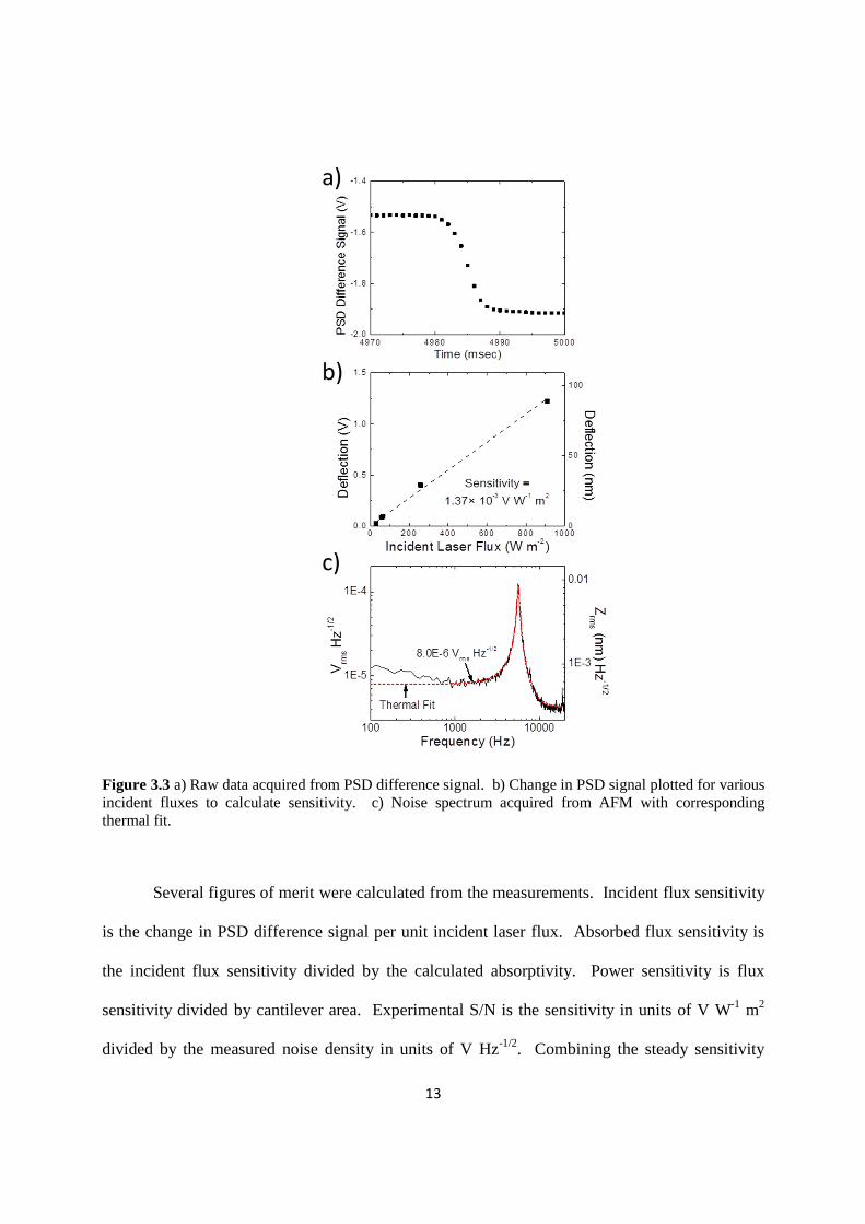
Figure 3.3a shows the raw PSD signal as a function of time. Measuring the time domain
signal was advantageous because it ensured that the full cantilever deflection was measured.
Turning the laser on and off led to rapid changes in the cantilever deflection signal. There was
12
some drift in the signal over time, but the drift was so slow that it had a negligible effect on the
cantilever response to the laser, which was very fast (<15 msec). Neutral density IR filters
attenuated the CO2 laser power which enabled the measurement of different magnitudes of
incident flux. Figure 3.3b shows several data points, each corresponding to a change in
deflection as shown in Figure 3.3a. The incident flux was found by measuring the power
through the aperture and dividing by aperture area. Figure 3.3b verifies the linear relationship
between cantilever bending and incident flux, which the model predicted.
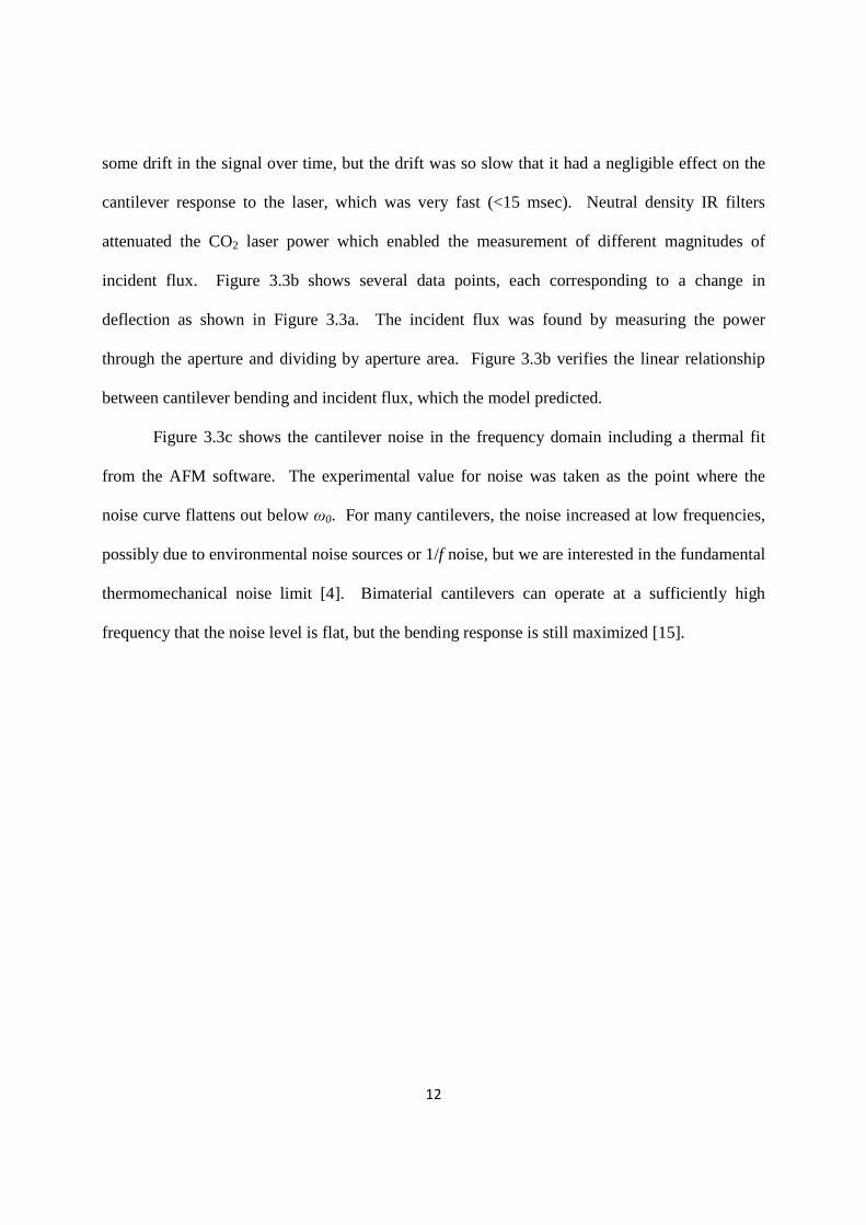
Figure 3.3c shows the cantilever noise in the frequency domain including a thermal fit
from the AFM software. The experimental value for noise was taken as the point where the
noise curve flattens out below ω0. For many cantilevers, the noise increased at low frequencies,
possibly due to environmental noise sources or 1/f noise, but we are interested in the fundamental
thermomechanical noise limit [4]. Bimaterial cantilevers can operate at a sufficiently high
frequency that the noise level is flat, but the bending response is still maximized [15].
13
Figure 3.3 a) Raw data acquired from PSD difference signal. b) Change in PSD signal plotted for various incident fluxes to calculate sensitivity. c) Noise spectrum acquired from AFM with corresponding thermal fit.
Several figures of merit were calculated from the measurements. Incident flux sensitivity
is the change in PSD difference signal per unit incident laser flux. Absorbed flux sensitivity is
the incident flux sensitivity divided by the calculated absorptivity. Power sensitivity is flux
sensitivity divided by cantilever area. Experimental S/N is the sensitivity in units of V W-1 m2
divided by the measured noise density in units of V Hz-1/2. Combining the steady sensitivity

14
measurement with the frequency domain noise measurement is relevant because in frequency
modulated bimaterial cantilever applications, the frequency can be low enough that the cantilever
reaches its steady deflection during each cycle [15].
15
CHAPTER 4: RESULTS AND DISCUSSION
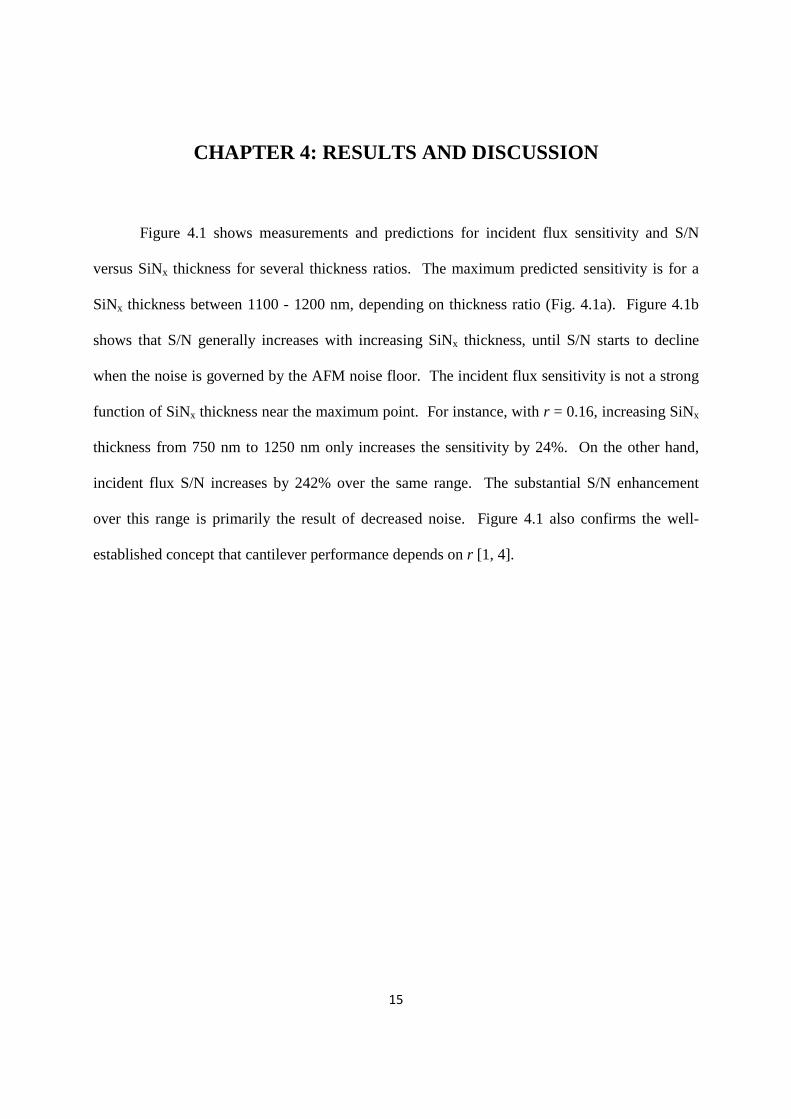
Figure 4.1 shows measurements and predictions for incident flux sensitivity and S/N
versus SiNx thickness for several thickness ratios. The maximum predicted sensitivity is for a
SiNx thickness between 1100 - 1200 nm, depending on thickness ratio (Fig. 4.1a). Figure 4.1b
shows that S/N generally increases with increasing SiNx thickness, until S/N starts to decline
when the noise is governed by the AFM noise floor. The incident flux sensitivity is not a strong
function of SiNx thickness near the maximum point. For instance, with r = 0.16, increasing SiNx
thickness from 750 nm to 1250 nm only increases the sensitivity by 24%. On the other hand,
incident flux S/N increases by 242% over the same range. The substantial S/N enhancement
over this range is primarily the result of decreased noise. Figure 4.1 also confirms the well-
established concept that cantilever performance depends on r [1, 4].
16
Figure 4.1 a) Comparison of model and experiment for incident flux sensitivity as a function of SiNx thickness. The thickness ratio r is the Al thickness divided by the SiNx thickness. b) Corresponding plot of S/N. The predictions are based on L=450 µm, W=40 µm, Q=10, and h=1000 W m-2 K-1. Black squares (r=0.05), red triangles pointing up (r=0.16), blue triangle pointing down (r=0.24), and magenta diamonds (r=0.37) are experimental data points.
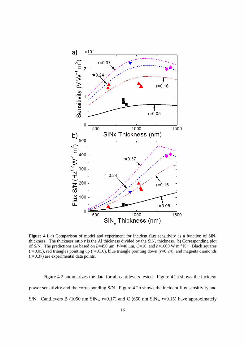
Figure 4.2 summarizes the data for all cantilevers tested. Figure 4.2a shows the incident
power sensitivity and the corresponding S/N. Figure 4.2b shows the incident flux sensitivity and
S/N. Cantilevers B (1050 nm SiNx, r=0.17) and C (650 nm SiNx, r=0.15) have approximately
17
the same incident power and flux sensitivities, but B has significantly higher S/N. Larger SiNx
thickness increases absorptivity and also decreases thermomechanical noise, which leads to
higher S/N.
Figure 4.2 Measured cantilever performance for all cantilevers tested in this work. a) Incident power sensitivity (black squares) and S/N (red triangles). b) Incident flux sensitivity (black squares) and S/N (red triangles).
18
A few commercially available AFM cantilevers were measured for comparison.
Cantilever β was chosen because it was predicted to have the best performance among the
commercial cantilevers we found [15]. Cantilever A achieves a 12X improvement for incident
flux sensitivity and a 21X improvement in S/N compared to cantilever β. The main reasons for
this improvement are that A has a thicker absorbing layer, a better material combination (SiNx/Al
compared to SiN/Au), and more absorbing area. Cantilever A also outperforms cantilever β by
6X for incident power S/N.
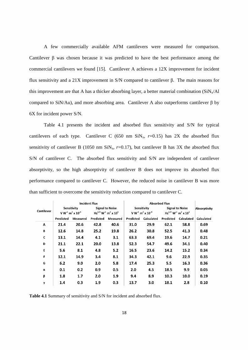
Table 4.1 presents the incident and absorbed flux sensitivity and S/N for typical
cantilevers of each type. Cantilever C (650 nm SiNx, r=0.15) has 2X the absorbed flux
sensitivity of cantilever B (1050 nm SiNx, r=0.17), but cantilever B has 3X the absorbed flux
S/N of cantilever C. The absorbed flux sensitivity and S/N are independent of cantilever
absorptivity, so the high absorptivity of cantilever B does not improve its absorbed flux
performance compared to cantilever C. However, the reduced noise in cantilever B was more
than sufficient to overcome the sensitivity reduction compared to cantilever C.
Table 4.1 Summary of sensitivity and S/N for incident and absorbed flux.

19
One application in which flux sensitivity is relevant is photothermal spectroscopy
because the cantilever area is smaller than the light source. Van Neste et al. measured absorption
spectra of explosive residues using bimaterial cantilever based photothermal spectroscopy [21].
Cantilever A has ~4X better incident flux sensitivity and S/N than the cantilever used in Ref.
[21].
Power sensitivity and minimum detectable power (inverse of S/N) are figures of merit
often used to compare bimaterial cantilevers. Varesi et al. reported a minimum detectable
absorbed power of 40 pW at a measurement bandwidth of 26 mHz [3]. Cantilever A has a
minimum detectable power of 4 pW for a measurement bandwidth of 26 mHz. Thus, cantilever
A has about 10X improved minimum detectable power compared to Ref. [3].
Detectivity, D*, is another figure of merit for radiation sensors and is defined as
* /cantD A N= where Acant is the cantilever area and N is the noise-spectral density [3]. Varesi
et al. demonstrated D* of 4.6×107 cm Hz1/2 W-1. In comparison, cantilever A has D* of 4.8×10⁸
cm Hz1/2 W-1, an improvement of about one order of magnitude.
Overall, the modeling and experiments show that the best bimaterial cantilever is not the
thinnest and most sensitive cantilever, but rather the cantilever that has the best combination of
sensitivity, noise, and absorptivity. Increasing the SiNx thickness improves infrared radiation
sensing performance by decreasing thermomechanical noise and increasing absorptivity. In
practice, the deflection measurement scheme will set the noise floor. Increasing SiNx thickness
to reduce thermomechanical noise below this noise floor will not decrease the overall
measurement noise and will eventually decrease S/N. The optimal SiNx thickness is a function
of thickness ratio, length, and width because these parameters also affect thermomechanical
20
noise and sensitivity. Figure 4.1b illustrates the change in optimal SiNx thickness for different
thickness ratios. As a result, the absolute values for optimal SiNx thickness presented here
should not be viewed as rigid design rules, but rather serve as a design guide.
21
CHAPTER 5: CONCLUSION
Optimization of silicon nitride thickness in silicon nitride-aluminum biomaterial
cantilevers leads to significant improvements in cantilever radiation sensing performance.
Increased silicon nitride thickness causes decreased thermomechanical noise and increased
absorptivity. The optimal silicon nitride thickness is a function of deflection measurement
scheme, cantilever length, cantilever width, and cantilever thickness ratio, so the optimal silicon
nitride thickness will vary depending on the application. Compared to the best commercial
cantilevers, cantilevers fabricated with L=450 µm, W=40 µm, r=0.37, and 1400 nm thick silicon
nitride achieved a 21X improvement in incident flux S/N and a 6X improvement in incident
power S/N.
22
REFERENCES
[1] J. Lai, T. Perazzo, Z. Shi, and A. Majumdar, "Optimization and performance of high-resolution
micro-optomechanical thermal sensors," Sensors and Actuators a-Physical, vol. 58, pp. 113-119,
Feb 1997.
[2] J. R. Barnes, R. J. Stephenson, M. E. Welland, C. Gerber, and J. K. Gimzewski, "Photothermal
Spectroscopy with Femtojoule Sensitivity Using a Micromechanical Device," Nature, vol. 372,
pp. 79-81, Nov 3 1994.
[3] J. Varesi, J. Lai, T. Perazzo, Z. Shi, and A. Majumdar, "Photothermal measurements at picowatt
resolution using uncooled micro-optomechanical sensors," Applied Physics Letters, vol. 71, pp.
306-308, Jul 21 1997.
[4] Y. Zhao, M. Y. Mao, R. Horowitz, A. Majumdar, J. Varesi, P. Norton, and J. Kitching,
"Optomechanical uncooled infrared imaging system: Design, microfabrication, and
performance," Journal of Microelectromechanical Systems, vol. 11, pp. 136-146, Apr 2002.
[5] T. Perazzo, M. Mao, O. Kwon, A. Majumdar, J. B. Varesi, and P. Norton, "Infrared vision using
uncooled micro-optomechanical camera," Applied Physics Letters, vol. 74, pp. 3567-3569, Jun 7
1999.
[6] S. R. Manalis, S. C. Minne, C. F. Quate, G. G. Yaralioglu, and A. Atalar, "Two-dimensional
micromechanical bimorph arrays for detection of thermal radiation," Applied Physics Letters, vol.
70, pp. 3311-3313, Jun 16 1997.
[7] P. G. Datskos, N. V. Lavrik, and S. Rajic, "Performance of uncooled microcantilever thermal
detectors," Review of Scientific Instruments, vol. 75, pp. 1134-1148, Apr 2004.
[8] B. Kwon, C. Wang, K. Park, R. Bhargava, and W. P. King, "Thermomechanical Sensitivity of
Microcantilevers in the Mid-Infrared Spectral Region," Nanoscale and Microscale
Thermophysical Engineering, vol. 15, pp. 16-27, 2011.

23
[9] M. K. Gunde and M. Macek, "Infrared optical constants and dielectric response functions of
silicon nitride and oxynitride films," Physica Status Solidi a-Applied Research, vol. 183, pp. 439-
449, Feb 2001.
[10] S. Timoshenko, "Analysis of Bi-Metal Thermostats," J. Opt. Soc. Am., vol. 11, pp. 233-255, 1925.
[11] F. P. Incropera and D. P. DeWitt, Fundamentals of heat and mass transfer: John Wiley, 2007.
[12] S. Shen, A. Narayanaswamya, S. Goh, and G. Chen, "Thermal conductance of bimaterial
microcantilevers," Applied Physics Letters, vol. 92, Feb 11 2008.
[13] M. Toda, T. Ono, F. Liu, and I. Voiculescu, "Evaluation of bimaterial cantilever beam for heat
sensing at atmospheric pressure," Review of Scientific Instruments, vol. 81, May 2010.
[14] A. Narayanaswamy and N. Gu, "Heat Transfer From Freely Suspended Bimaterial
Microcantilevers," Journal of Heat Transfer-Transactions of the Asme, vol. 133, Apr 2011.
[15] B. Kwon, M. Rosenberger, R. Bhargava, D. G. Cahill, and W. P. King, "Dynamic
thermomechanical response of bimaterial microcantilevers to periodic heating by infrared
radiation," Review of Scientific Instruments, vol. 83, pp. 015003-015003-7-015003-015003-7,
2012.
[16] H. J. Butt and M. Jaschke, "Calculation of Thermal Noise in Atomic-Force Microscopy,"
Nanotechnology, vol. 6, pp. 1-7, Jan 1995.
[17] R. R. Craig and T. A. C. O. N. Philpot, Mechanics of Materials: John Wiley & Sons, 2011.
[18] P. Yeh, Optical waves in layered media: Wiley, 1988.
[19] F. Jutzi, D. H. B. Wicaksono, G. Pandraud, N. de Rooij, and P. J. French, "Far-infrared sensor
with LPCVD-deposited low-stress Si-rich nitride absorber membrane-Part 1. Optical
absorptivity," Sensors and Actuators a-Physical, vol. 152, pp. 119-125, Jun 18 2009.
[20] M. V. Salapaka, H. S. Bergh, J. Lai, A. Majumdar, and E. McFarland, "Multi-mode noise analysis
of cantilevers for scanning probe microscopy," Journal of Applied Physics, vol. 81, pp. 2480-
2487, Mar 15 1997.
24
[21] C. W. Van Neste, L. R. Senesac, D. Yi, and T. Thundat, "Standoff detection of explosive residues
using photothermal microcantilevers," Applied Physics Letters, vol. 92, Mar 31 2008.
[22] E. A. Wachter, T. Thundat, P. I. Oden, R. J. Warmack, P. G. Datskos, and S. L. Sharp, "Remote
optical detection using microcantilevers," Review of Scientific Instruments, vol. 67, pp. 3434-
3439, Oct 1996.
[23] D. Sarid, Scanning force microscopy: with applications to electric, magnetic, and atomic forces:
Oxford University Press, 1994.
[24] C. Iliescu, F. E. H. Tay, and J. S. Wei, "Low stress PECVD-SiNx layers at high deposition rates
using high power and high frequency for MEMS applications," Journal of Micromechanics and
Microengineering, vol. 16, pp. 869-874, Apr 2006.