© IMEC 2011 - ESA Microelectronics Section...
69
© IMEC 2011
Transcript of © IMEC 2011 - ESA Microelectronics Section...

© IMEC 2011
© IMEC 2011
IMEC ASIC SERVICES
EUROPRACTICE
ESA : 15th Feb 2010
Danny Lambrichts
© IMEC 2011
Outline
General FM procurement
FM qualification of a Dare 180 nm Mixed signal Asic
3
© IMEC 2011
Manufacturing
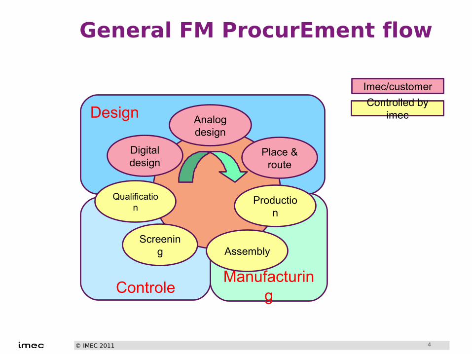
General FM ProcurEment flow
4
Design
Controle
Digital design
Analog design
Place & route
Production
Screening
Qualification
Assembly
Imec/customer
Controlled by imec
© IMEC 2011
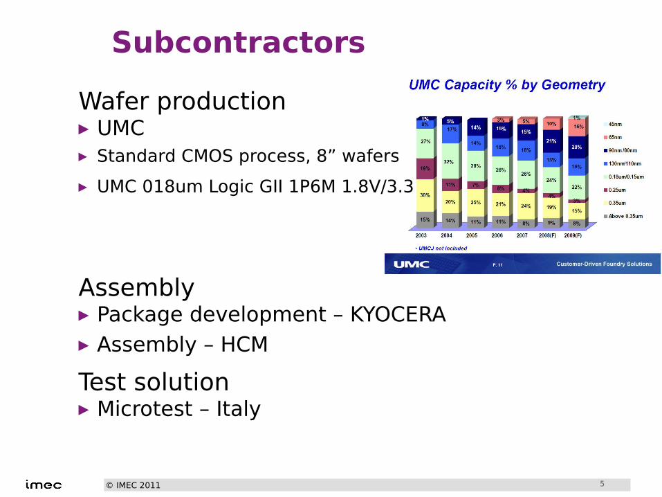
Subcontractors
Wafer production▸ UMC▸ Standard CMOS process, 8” wafers
▸ UMC 018um Logic GII 1P6M 1.8V/3.3
Assembly▸ Package development – KYOCERA▸ Assembly – HCM
Test solution▸ Microtest – Italy
5
© IMEC 2011
Subcontractors
Qualification▸ HCM - Assembly▸ Microtest – Electrical tests/HTOL▸ Maser Engineering – environmental tests▸ Maprad - Radiation tests
6
© IMEC 2011
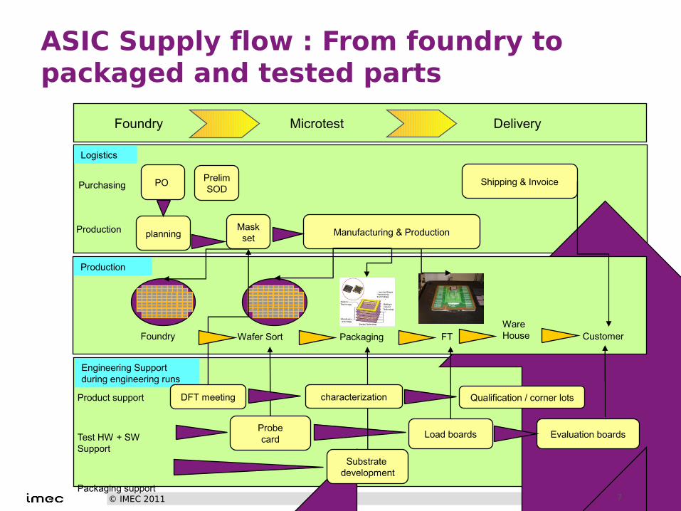
ASIC Supply flow : From foundry to packaged and tested parts
Logistics
Purchasing
Production
PO PrelimSOD
planningMaskset
Shipping & Invoice
Manufacturing & Production
Foundry Wafer Sort Packaging FTWare House Customer
Production
Engineering Support during engineering runs
Foundry Microtest Delivery
Product support
Test HW + SW Support
Packaging support
Probecard
Substrate development
Load boards
DFT meeting Qualification / corner lotscharacterization
Evaluation boards
7
© IMEC 2011
Outline
General FM procurement
FM qualification of a Dare 180 nm Mixed signal Asic
8
© IMEC 2011
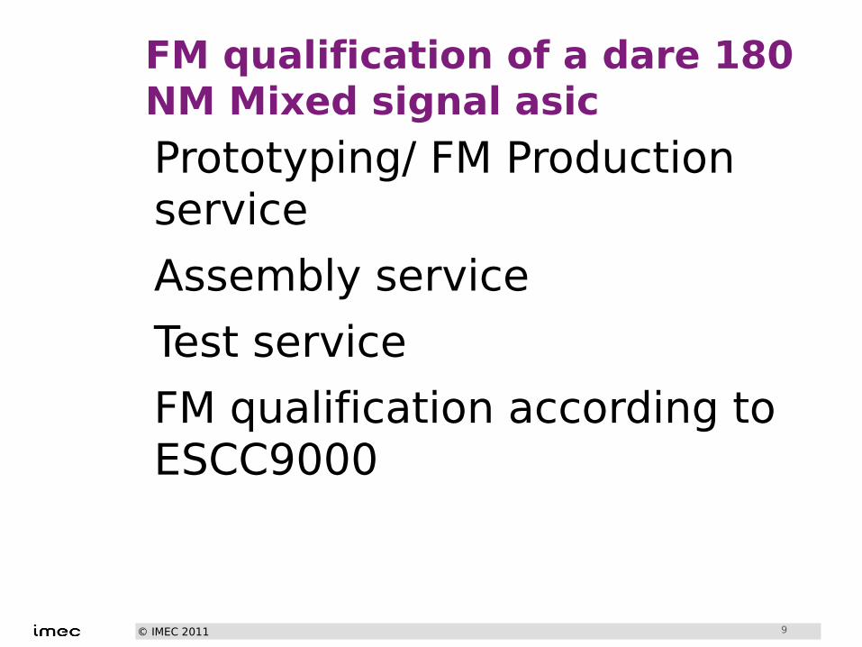
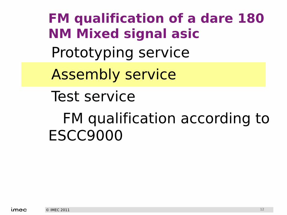
FM qualification of a dare 180 NM Mixed signal asic Prototyping/ FM Production service
Assembly service Test service FM qualification according to ESCC9000
9
© IMEC 2011
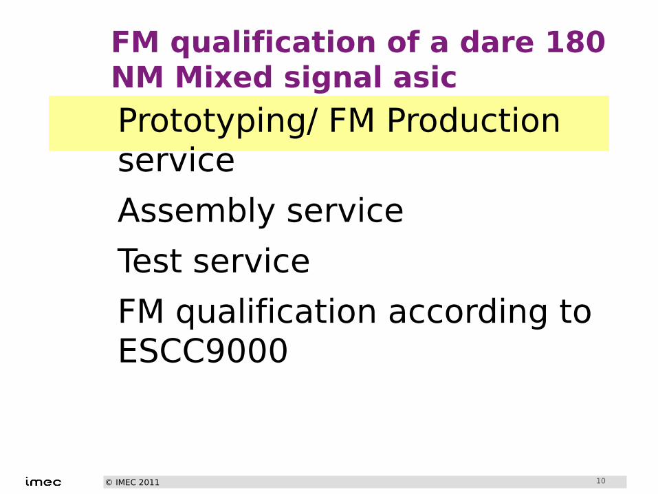
FM qualification of a dare 180 NM Mixed signal asic Prototyping/ FM Production service
Assembly service Test service FM qualification according to ESCC9000
10
© IMEC 2011
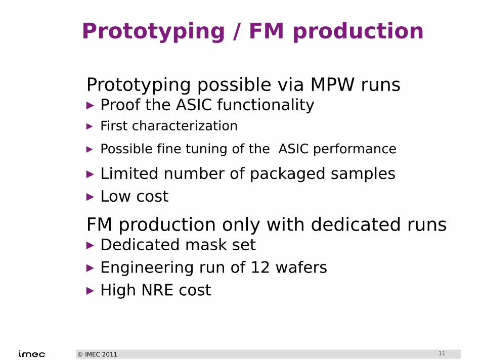
Prototyping / FM production
Prototyping possible via MPW runs▸ Proof the ASIC functionality▸ First characterization
▸ Possible fine tuning of the ASIC performance
▸ Limited number of packaged samples▸ Low cost
FM production only with dedicated runs▸ Dedicated mask set▸ Engineering run of 12 wafers▸ High NRE cost
11
© IMEC 2011
FM qualification of a dare 180 NM Mixed signal asic Prototyping service Assembly service Test service
FM qualification according to ESCC9000
12
© IMEC 2011
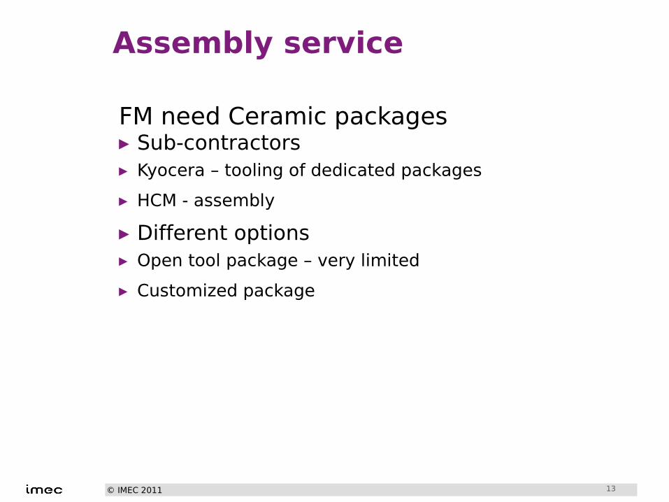
Assembly service
FM need Ceramic packages ▸ Sub-contractors▸ Kyocera – tooling of dedicated packages
▸ HCM - assembly
▸ Different options▸ Open tool package – very limited
▸ Customized package
13
© IMEC 2011
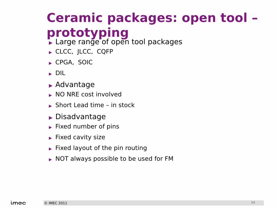
Ceramic packages: open tool – prototyping▸ Large range of open tool packages▸ CLCC, JLCC, CQFP
▸ CPGA, SOIC
▸ DIL
▸ Advantage▸ NO NRE cost involved
▸ Short Lead time – in stock
▸ Disadvantage▸ Fixed number of pins
▸ Fixed cavity size
▸ Fixed layout of the pin routing
▸ NOT always possible to be used for FM
14
© IMEC 2011
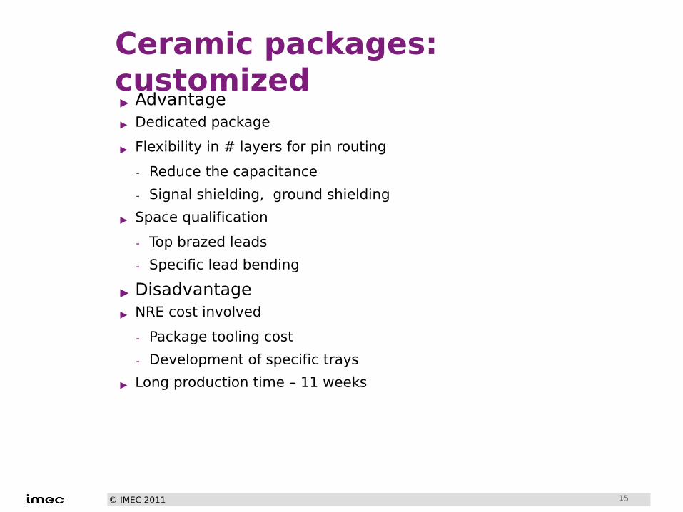
Ceramic packages: customized▸ Advantage▸ Dedicated package
▸ Flexibility in # layers for pin routing
- Reduce the capacitance
- Signal shielding, ground shielding
▸ Space qualification
- Top brazed leads
- Specific lead bending
▸ Disadvantage▸ NRE cost involved
- Package tooling cost
- Development of specific trays
▸ Long production time – 11 weeks
15
© IMEC 2011
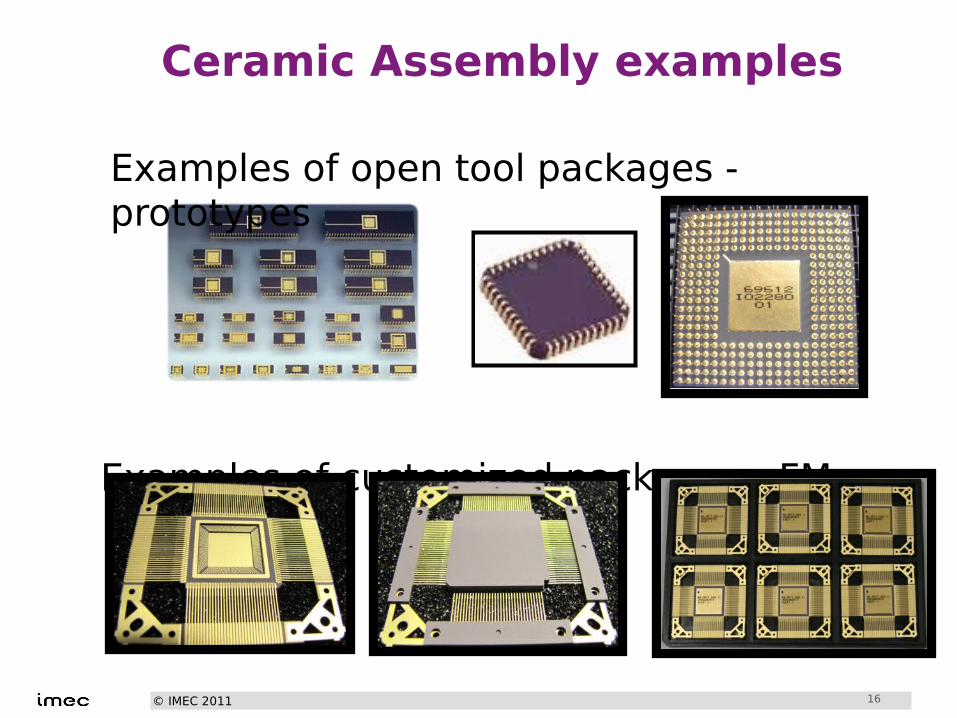
Ceramic Assembly examples
Examples of open tool packages - prototypes
Examples of customized packages - FM
16
© IMEC 2011
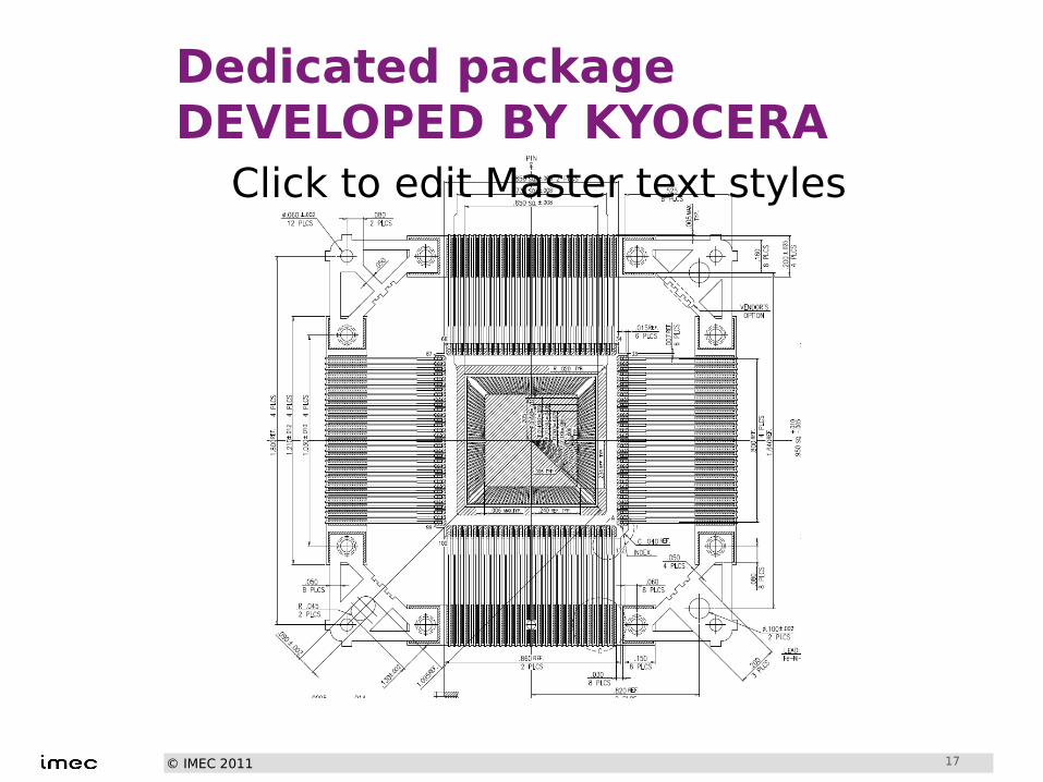
Dedicated package DEVELOPED BY KYOCERA
17
Click to edit Master text styles
© IMEC 2011
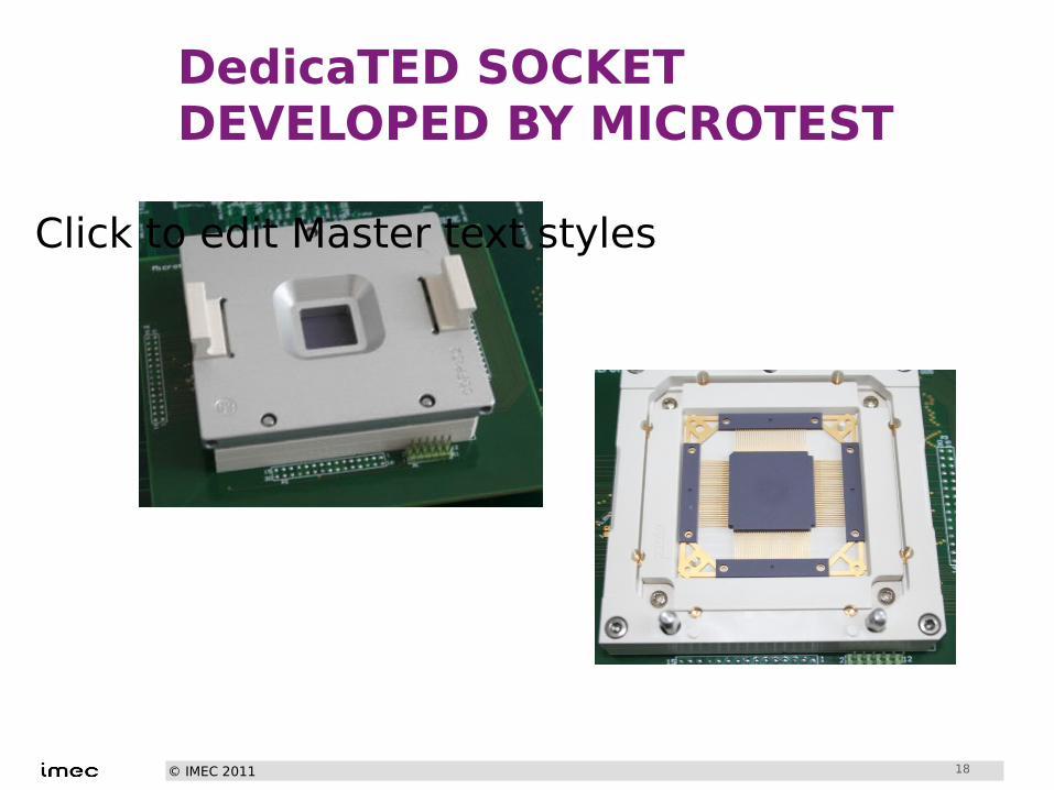
DedicaTED SOCKET DEVELOPED BY MICROTEST
18
Click to edit Master text styles
© IMEC 2011
FM qualification of a dare 180 NM Mixed signal asic Prototyping Assembly Test service FM qualification according to ESCC9000
19
© IMEC 2011
test service
▸ Test facility and capabilities
▸ Test flow
▸ Failure Analysis
20
© IMEC 2011
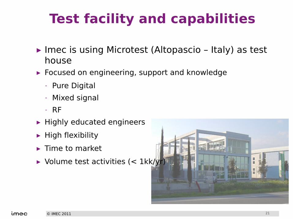
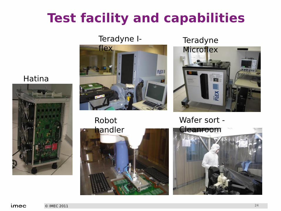
Test facility and capabilities
▸ Imec is using Microtest (Altopascio – Italy) as test house
▸ Focused on engineering, support and knowledge
- Pure Digital
- Mixed signal
- RF
▸ Highly educated engineers
▸ High flexibility
▸ Time to market
▸ Volume test activities (< 1kk/yr)
21
© IMEC 2011
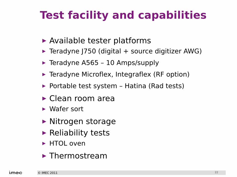
Test facility and capabilities
▸ Available tester platforms▸ Teradyne J750 (digital + source digitizer AWG)
▸ Teradyne A565 – 10 Amps/supply
▸ Teradyne Microflex, Integraflex (RF option)
▸ Portable test system – Hatina (Rad tests)
▸ Clean room area▸ Wafer sort
▸ Nitrogen storage▸ Reliability tests▸ HTOL oven
▸ Thermostream
22
© IMEC 2011 23
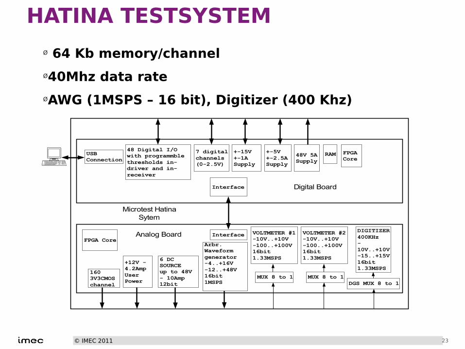
HATINA TESTSYSTEM
Ø 64 Kb memory/channel
Ø40Mhz data rate
ØAWG (1MSPS – 16 bit), Digitizer (400 Khz)
6 DCSOURCEup to 48V- 10Amp12bit
VOLTMETER #1-10V..+10V-100..+100V16bit1.33MSPS
VOLTMETER #2-10V..+10V-100..+100V16bit1.33MSPS
DIGITIZER400KHz-10V..+10V-15..+15V16bit1.33MSPS
MUX 8 to 1
Arbr.Waveformgenerator-4..+16V-12..+48V16bit1MSPS DGS MUX 8 to 1
+12V -4.2AmpUserPower
1603V3CMOSchannel
USBConnection
48 Digital I/Owith programmblethresholds in-driver and in-receiver
FPGA Core
7 digitalchannels(0-2.5V)
+-15V+-1ASupply
+-5V+-2.5ASupply
48V 5ASupply
FPGACore
Interface
RAM
Interface
MUX 8 to 1
Analog Board
Digital Board
Microtest HatinaSytem
© IMEC 2011
Test facility and capabilities
24
Hatina
Teradyne I-flex
Teradyne Microflex
Wafer sort - Cleanroom
Robot handler
© IMEC 2011
test service
▸ Test facility and capabilities
▸ Test flow
▸ Failure Analysis
25
© IMEC 2011
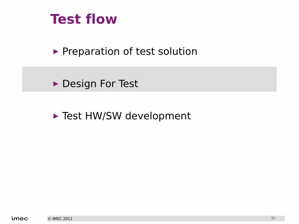
Test flow
▸ Preparation of test solution
▸ Design For Test
▸ Test HW/SW development
26
© IMEC 2011
Test flow
▸ Preparation of test solution
▸ Design For Test
▸ Test HW/SW development
27
© IMEC 2011
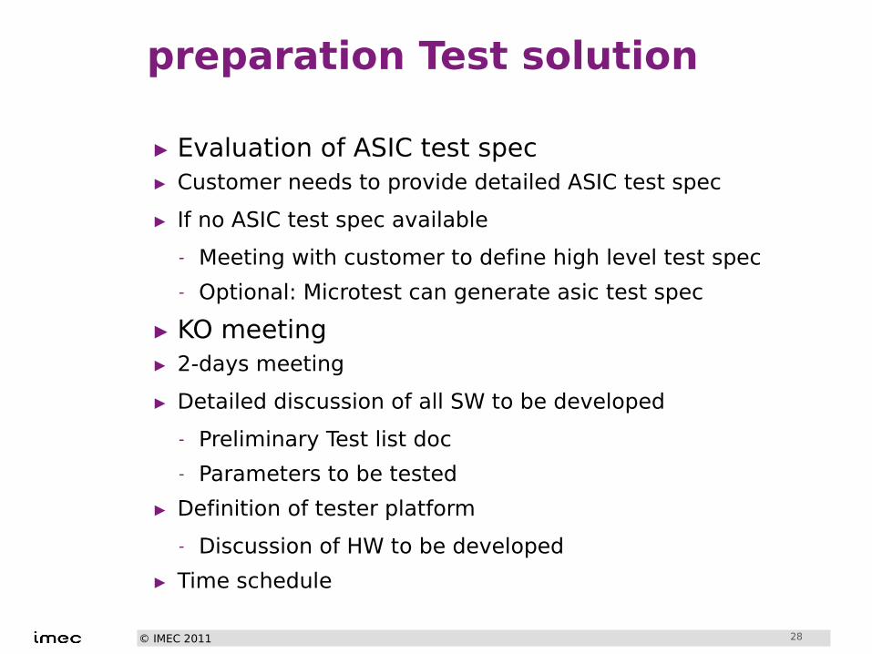
preparation Test solution
▸ Evaluation of ASIC test spec▸ Customer needs to provide detailed ASIC test spec
▸ If no ASIC test spec available
- Meeting with customer to define high level test spec
- Optional: Microtest can generate asic test spec
▸ KO meeting▸ 2-days meeting
▸ Detailed discussion of all SW to be developed
- Preliminary Test list doc
- Parameters to be tested
▸ Definition of tester platform
- Discussion of HW to be developed
▸ Time schedule
28
© IMEC 2011
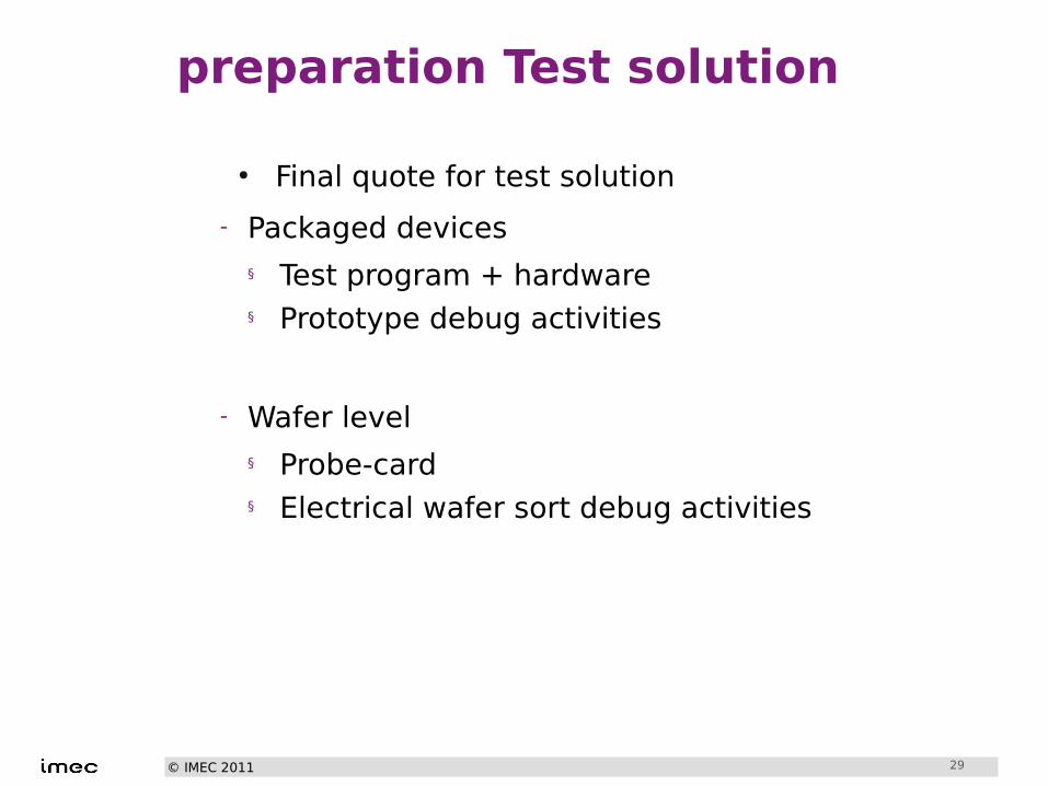
preparation Test solution
● Final quote for test solution
- Packaged devices § Test program + hardware§ Prototype debug activities
- Wafer level§ Probe-card§ Electrical wafer sort debug activities
29
© IMEC 2011
Test flow
▸ Preparation of test solution
▸ Design For Test
▸ Test HW/SW development
30
© IMEC 2011
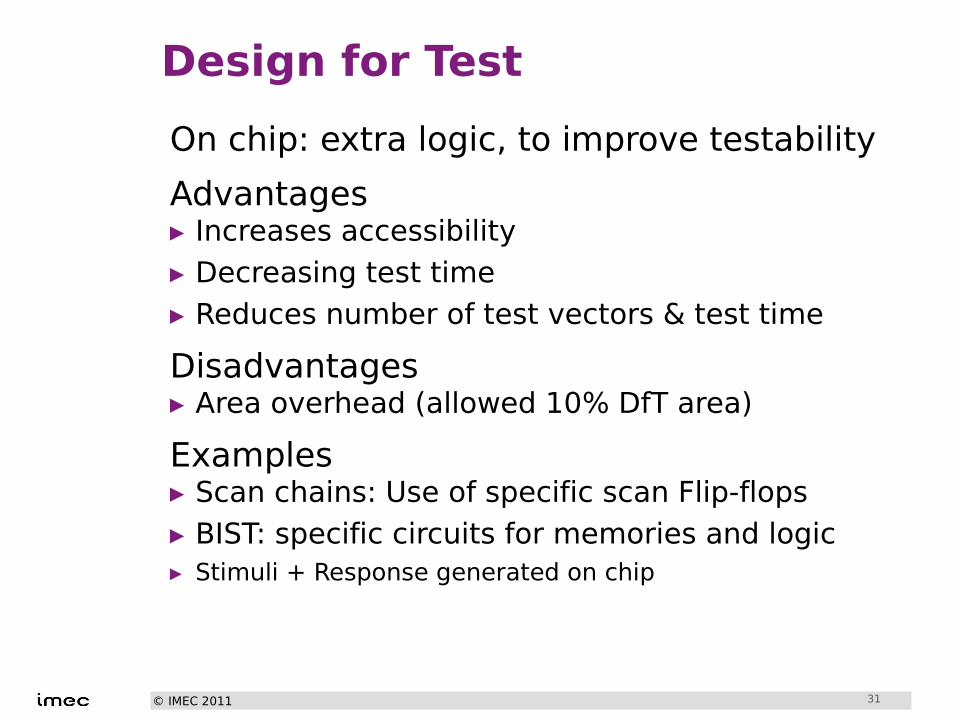
Design for Test
On chip: extra logic, to improve testability Advantages▸ Increases accessibility
▸ Decreasing test time
▸ Reduces number of test vectors & test time
Disadvantages▸ Area overhead (allowed 10% DfT area)
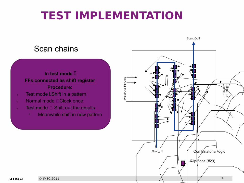
Examples▸ Scan chains: Use of specific scan Flip-flops
▸ BIST: specific circuits for memories and logic▸ Stimuli + Response generated on chip
31
© IMEC 2011
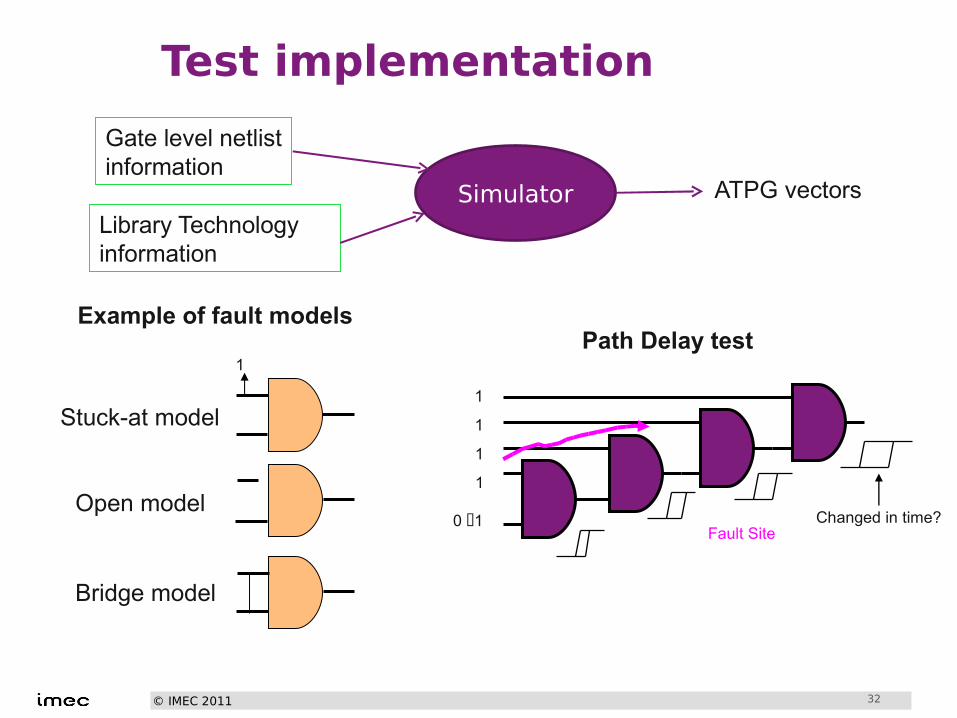
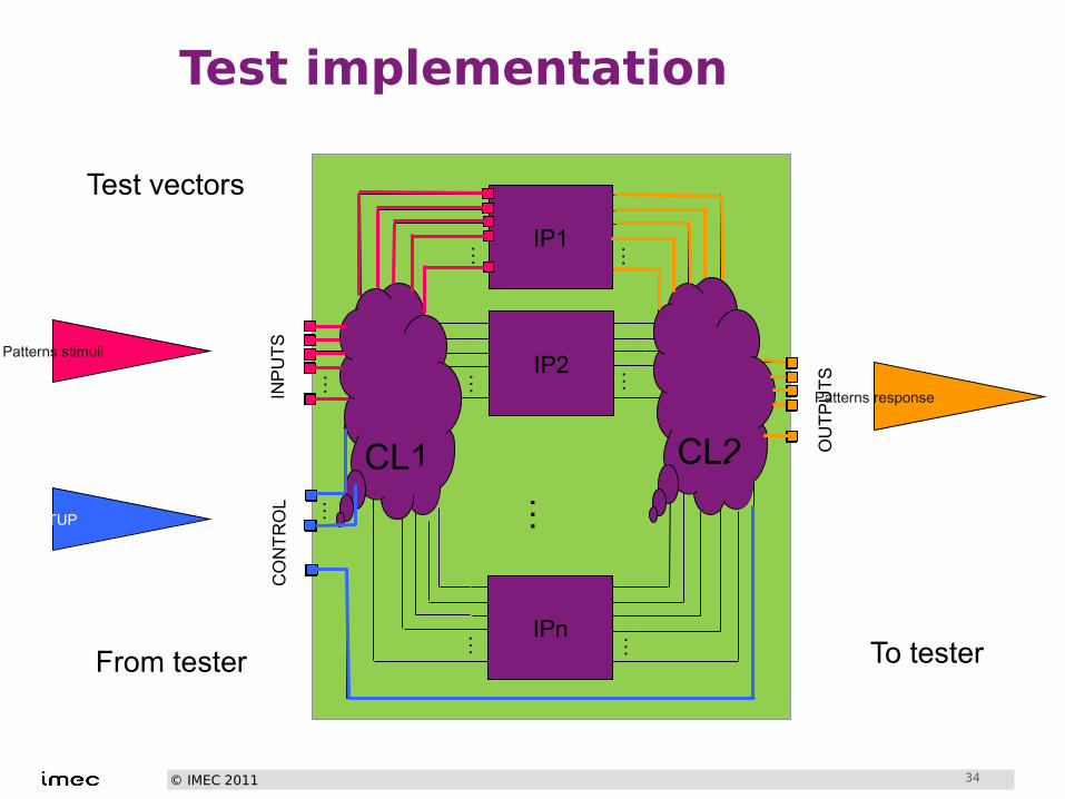
Test implementation
32
1
Fault Site
1
1
1
1
0 1 Changed in time?
Stuck-at model
Open model
Bridge model
Path Delay testExample of fault models
ATPG vectorsSimulator
Gate level netlistinformation
Library Technologyinformation
© IMEC 2011
TEST IMPLEMENTATION
33
Scan_IN
Scan_OUT
PR
IMA
RY
IN
PU
TS
PR
IMA
RY
O
UT
PU
TS
Combinatorial logic
Flip-flops (#29)
Scan chains
In test mode
FFs connected as shift register
Procedure:
1. Test mode Shift in a pattern
2. Normal mode Clock once
3. Test mode Shift out the results § Meanwhile shift in new pattern
© IMEC 2011
Test implementation
34
INP
UT
SC
ON
TR
OL
……
……
IP1
IP2
IPn
CL2CL1
……
……
………
…
OU
TP
UT
S
Patterns response
SETUP
Patterns stimuli
From tester To tester
Test vectors
© IMEC 2011
Test flow
▸ Preparation of test solution
▸ Design For Test
▸ Test HW/SW development
35
© IMEC 2011
Test HW and sw development
▸ HW development for Final test / Wafer sort▸ Schematic entry/layout of load boards
▸ Manufacturing of load boards (rider board/ large board)
▸ SW development off-line▸ Test pattern conversion
▸ Test pattern generation
- Dedicated test routines for analog tests
▸ SW development on-line▸ Debug of ASIC
▸ ASIC characterization▸ ESD & LU tests
▸ Characterization on 30 samples
▸ Data logs, data correlation, Final definition test windows36
© IMEC 2011
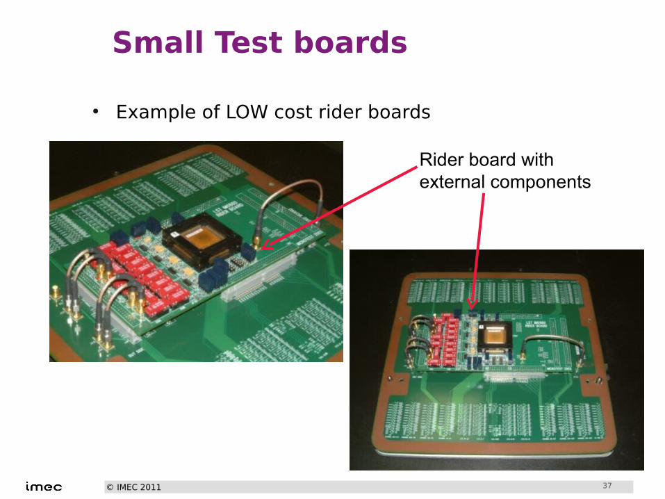
Small Test boards
● Example of LOW cost rider boards
Rider board with external components
37
© IMEC 2011
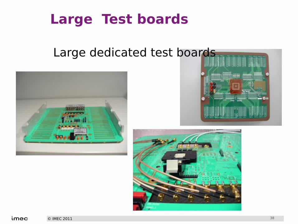
Large Test boards
38
Large dedicated test boards
© IMEC 2011
Wafer probing
39
Remove bad dies in early manufacturing stage▸ Advantage Save packaging cost▸ Failure due to functionality (electrical) or processing
Resources
▸ Tester & Test program▸ Through channel stimuli & compare with expected response▸ Generates data logs for analysis
▸ Binning; Classify the error VS test type
▸ Probe card▸ interface between die and tester channels
Test flow▸ Bad dies Inked for identification + Wafer maps
▸ Good dies After sawing packaging
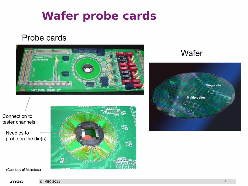
© IMEC 2011
Wafer probe cards
40
Connection totester channels
Needles to probe on the die(s)
Probe cards
Wafer
(Courtesy of Microtest)
© IMEC 2011
asic test service
▸ Test facility and capabilities
▸ Test flow
▸ Failure Analysis
41
© IMEC 2011
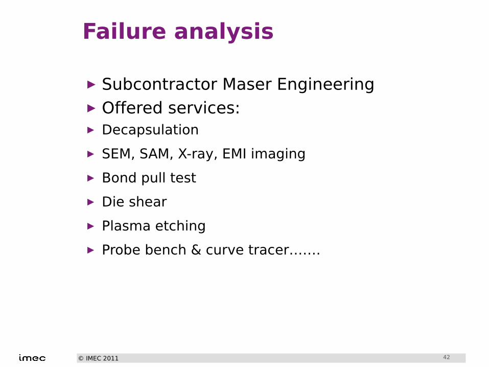
Failure analysis
▸ Subcontractor Maser Engineering▸ Offered services:▸ Decapsulation
▸ SEM, SAM, X-ray, EMI imaging
▸ Bond pull test
▸ Die shear
▸ Plasma etching
▸ Probe bench & curve tracer…….
42
© IMEC 2011
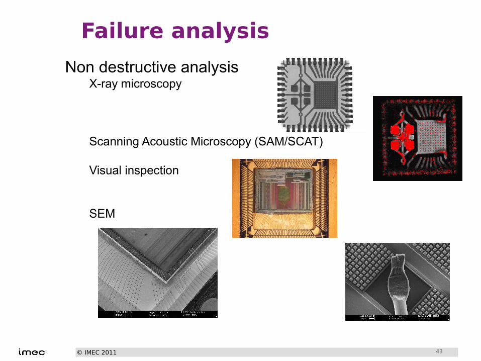
Failure analysis
43
Non destructive analysisX-ray microscopy
Scanning Acoustic Microscopy (SAM/SCAT)
Visual inspection
SEM
© IMEC 2011
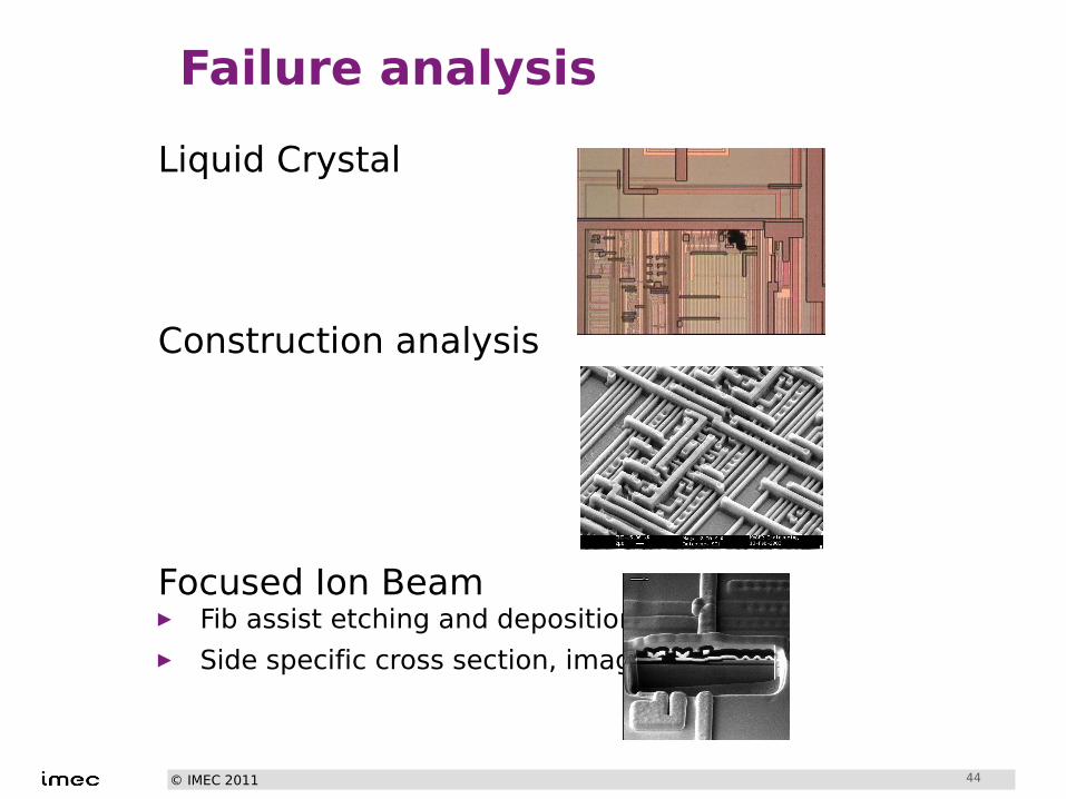
Failure analysis
44
Liquid Crystal
Construction analysis
Focused Ion Beam▸ Fib assist etching and deposition
▸ Side specific cross section, imaging
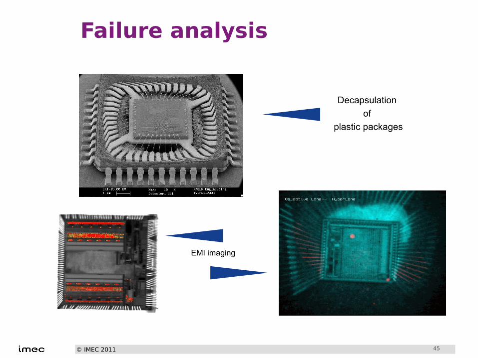
© IMEC 2011
Failure analysis
Decapsulation
of
plastic packages
EMI imaging
45
© IMEC 2011
FM qualification of a dare 180 NM Mixed signal asic Prototyping Assembly Test service FM qualification according to ESCC9000
46
© IMEC 2011
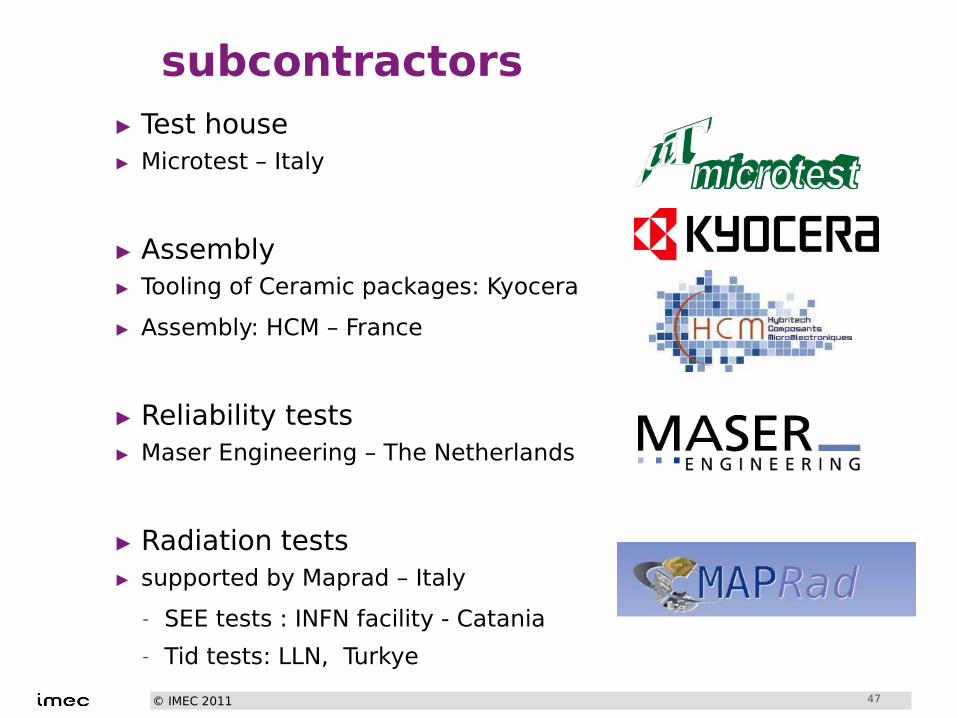
subcontractors▸ Test house ▸ Microtest – Italy
▸ Assembly▸ Tooling of Ceramic packages: Kyocera
▸ Assembly: HCM – France
▸ Reliability tests▸ Maser Engineering – The Netherlands
▸ Radiation tests▸ supported by Maprad – Italy
- SEE tests : INFN facility - Catania
- Tid tests: LLN, Turkye
47
© IMEC 2011
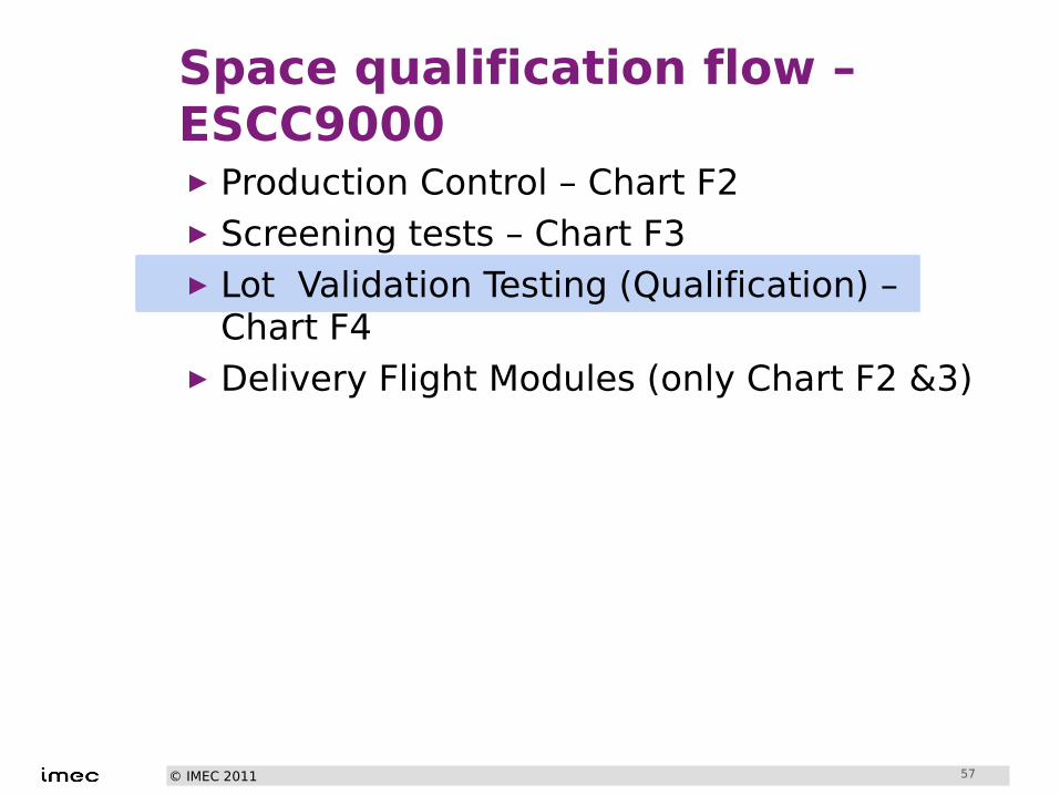
Space qualification flow – ESCC9000▸ Production Control – Chart F2▸ Screening tests – Chart F3▸ Lot Validation Testing (Qualification) –
Chart F4▸ Delivery Flight Modules (only Chart F2 &3)
48
© IMEC 2011
Space qualification flow – ESCC9000▸ Production Control – Chart F2▸ Screening tests – Chart F3▸ Lot Validation Testing (Qualification) –
Chart F4▸ Delivery Flight Modules (only Chart F2 &3)
49
© IMEC 2011
Detailed ESCC9000 flow
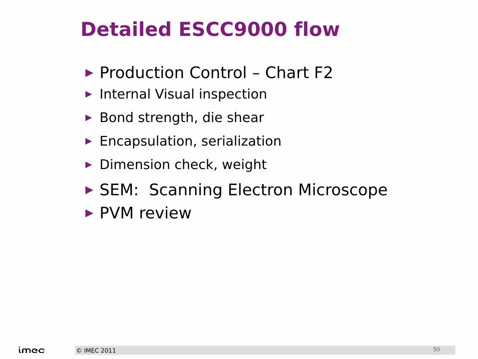
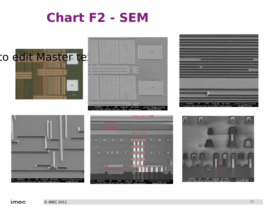
▸ Production Control – Chart F2▸ Internal Visual inspection
▸ Bond strength, die shear
▸ Encapsulation, serialization
▸ Dimension check, weight
▸ SEM: Scanning Electron Microscope▸ PVM review
50
© IMEC 2011
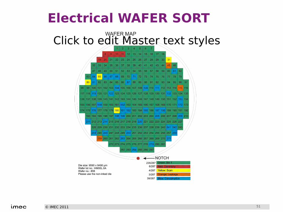
Electrical WAFER SORT
51
Click to edit Master text styles
© IMEC 2011
Chart F2 - SEM
52
Click to edit Master text styles
© IMEC 2011
Space qualification flow – ESCC9000▸ Production Control – Chart F2▸ Screening tests – Chart F3▸ Lot Validation Testing (Qualification) –
Chart F4▸ Delivery Flight Modules (only Chart F2 &3)
53
© IMEC 2011
Detailed ESCC9000 flow
▸ Screening tests – Chart F3▸ Electrical test @ HT, RT, LT
- HTS (24 hrs @ 150 degrees)
- TCT (-65/150 degrees, 10 cycles)
- PIND (MIL STD-883, meth 2020, cond A)
▸ Functional test @ HT, RT, LT – Parameter Drift Analysis
- Power Burn-in (240 hrs @ 125 degrees)
▸ Functional test @ HT, RT, LT - Parameter Drift Analysis
- Fine & gross leak
- Ext Vis inspection
- Solderability
54
© IMEC 2011
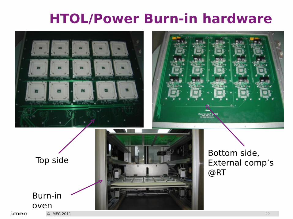
HTOL/Power Burn-in hardware
55
Bottom side,External comp’s @RT
Top side
Burn-in oven
© IMEC 2011
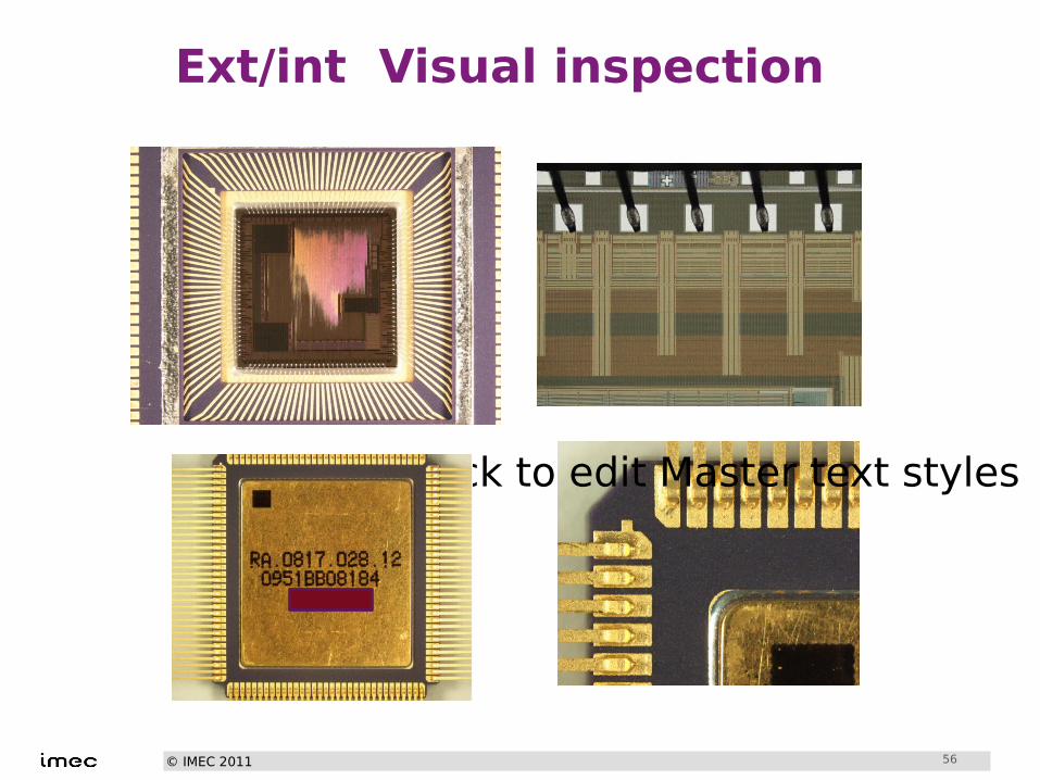
Ext/int Visual inspection
56
Click to edit Master text styles
© IMEC 2011
Space qualification flow – ESCC9000▸ Production Control – Chart F2▸ Screening tests – Chart F3▸ Lot Validation Testing (Qualification) –
Chart F4▸ Delivery Flight Modules (only Chart F2 &3)
57
© IMEC 2011
Detailed ESCC9000 flow
▸ Lot Validation testing – Chart F4▸ Endurance test 1, on 15 devices
- HTOL – 2000 hrs, with intermediate tests @500, 1000 hrs
- Fine & gross leak
- Test @RT, HT, LT- Ext Visp
▸ Environmental test 1, 15 devices
- Mechanical shock, Vibration
- Constant acceleration, fine& gross leak
- Test @RT, EXT visp
▸ Environmental test 2, 15 devices
- Thermal shock
- Moisture resistance
- Fine & gross leak,
- Test @RT, Ext Vis Insp58
© IMEC 2011
Detailed ESCC9000 flow
● Assembly tests
- Permanence of marking
- Terminal strength, Internal Visp
- Die shear
- bond pull, bond shear● Rad test boards
- Tid tests (Total Ionizing Dose)§ Tid test board§ Func test board on Hatina test system
- SEE tests (Single Event Effects)§ SEE test board (3 sockets)§ Func test board on Hatina test system
59
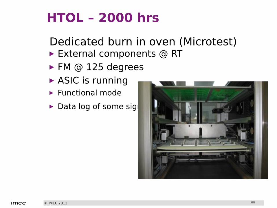
© IMEC 2011
HTOL – 2000 hrs
60
Dedicated burn in oven (Microtest)▸ External components @ RT▸ FM @ 125 degrees▸ ASIC is running▸ Functional mode
▸ Data log of some signals
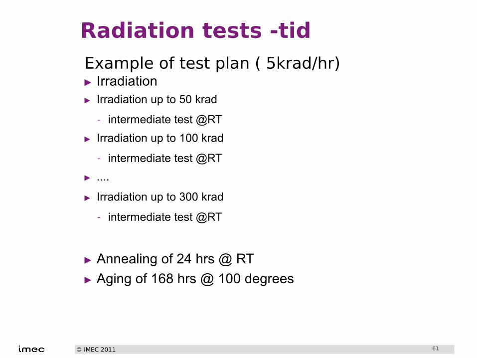
© IMEC 2011
Radiation tests -tid Example of test plan ( 5krad/hr)▸ Irradiation▸ Irradiation up to 50 krad
- intermediate test @RT
▸ Irradiation up to 100 krad
- intermediate test @RT
▸ ....
▸ Irradiation up to 300 krad
- intermediate test @RT
▸ Annealing of 24 hrs @ RT
▸ Aging of 168 hrs @ 100 degrees
61
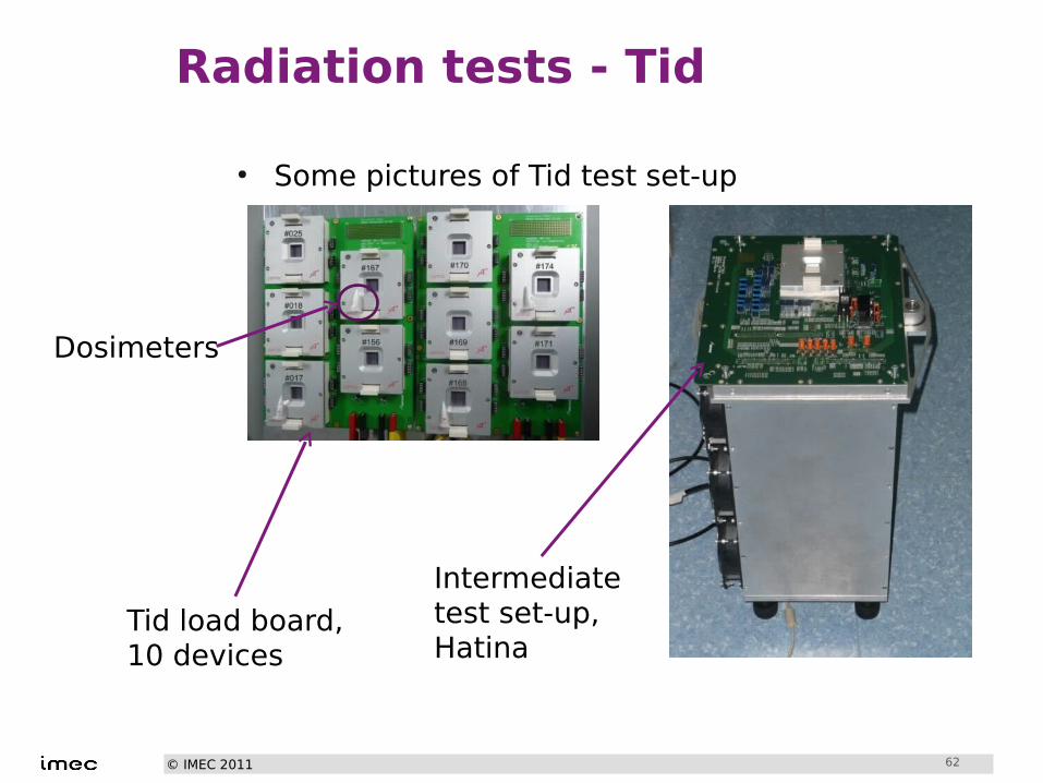
© IMEC 2011
Radiation tests - Tid
● Some pictures of Tid test set-up
Tid load board,10 devices
Dosimeters
Intermediate test set-up, Hatina
62
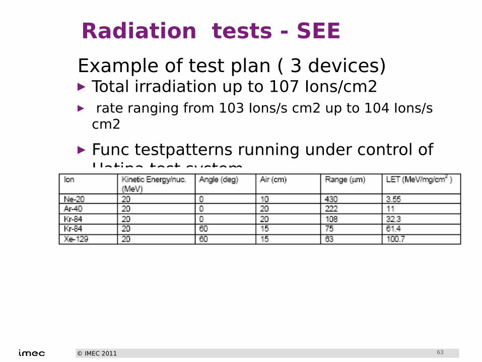
© IMEC 2011
Radiation tests - SEE Example of test plan ( 3 devices)▸ Total irradiation up to 107 Ions/cm2 ▸ rate ranging from 103 Ions/s cm2 up to 104 Ions/s
cm2
▸ Func testpatterns running under control of Hatina test system
63
© IMEC 2011
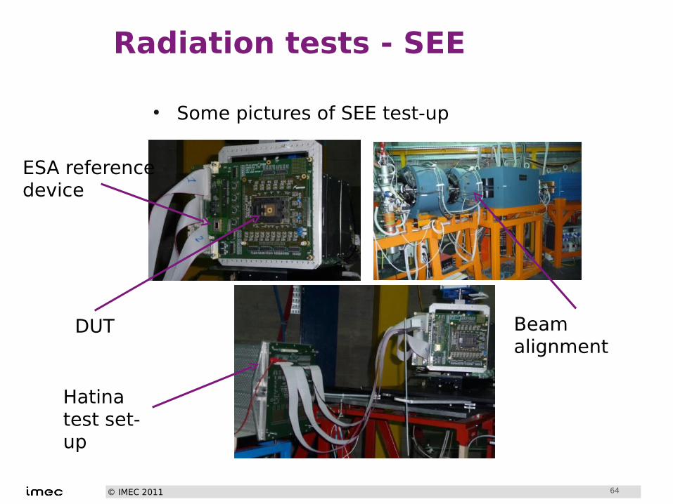
Radiation tests - SEE
● Some pictures of SEE test-up
DUT Beam alignment
Hatina test set-up
ESA referencedevice
64
© IMEC 2011
Space qualification flow – ESCC9000▸ Production Control – Chart F2▸ Screening tests – Chart F3▸ Lot Validation Testing (Qualification) –
Chart F4▸ Delivery Flight Modules (only Chart F2 &3)
65
© IMEC 2011
FM’s delivery
All devices for FM’s will be screened▸ Assembly according chart F2▸ Electrical test and reliability tests
according to chart F3.
66
© IMEC 2011
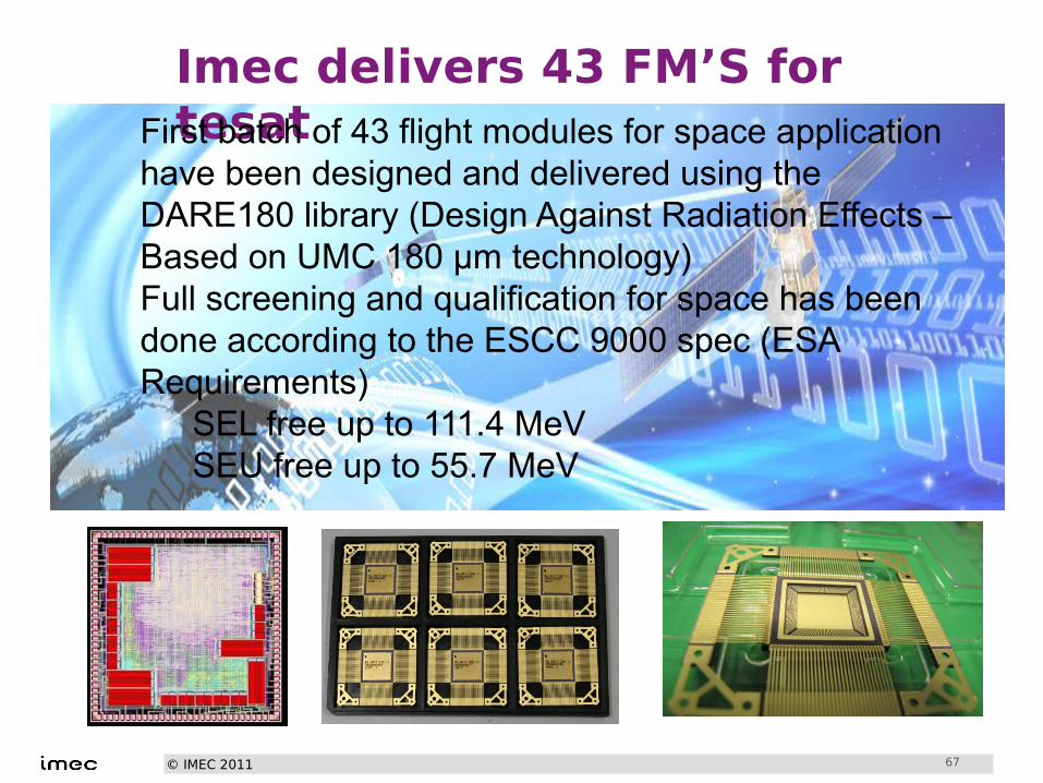
Imec delivers 43 FM’S for tesat
67
First batch of 43 flight modules for space application have been designed and delivered using the DARE180 library (Design Against Radiation Effects – Based on UMC 180 µm technology)Full screening and qualification for space has been done according to the ESCC 9000 spec (ESA Requirements)
SEL free up to 111.4 MeVSEU free up to 55.7 MeV
© IMEC 2011
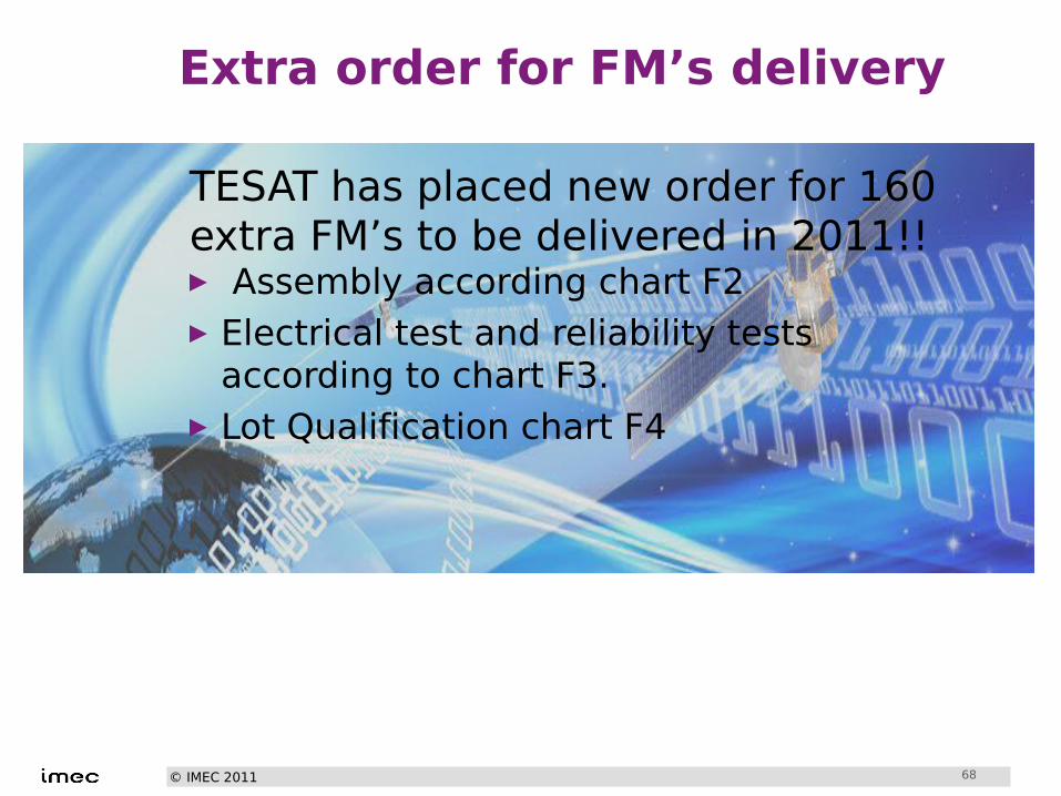
Extra order for FM’s delivery
TESAT has placed new order for 160 extra FM’s to be delivered in 2011!!▸ Assembly according chart F2▸ Electrical test and reliability tests
according to chart F3.▸ Lot Qualification chart F4
68
© IMEC 2011
statements
Design in 90, 65, 40nm is becoming increasingly complex : GDS prep and check crucial for error-free tape out
Design within corners to assure first-time right success
Test and qualification: increasingly important
69