III-V FET Channel Designs for High Current Densities and Thin Inversion Layers [email protected]...
34
III-V FET Channel Designs for High Current Densities and Thin Inversion Layers [email protected] 805-893-3244, 805-893-5705 fax Mark Rodwell University of California, Santa Barbara Coauthors: W. Frensley: University of Texas, Dallas S. Steiger, S. Lee, Y. Tan, G. Hegde, G. Klimek Network for Computational Nanotechnology, Purdue University E. Chagarov, L. Wang, P. Asbeck, A. Kummel, University of California, San Diego T. Boykin University of Alabama, Huntsville J. N. Schulman The Aerospace Corporation, El Segundo, CA. 2010 IEEE Device Research Conference, June 21-23, Notre Dame, Indiana Acknowledgements: Herb Kroemer (UCSB), Bobby Brar (Teledyne) Art Gossard (UCSB), John Albrecht (DARPA)
-
Upload
kerry-adams -
Category
Documents
-
view
219 -
download
0
Transcript of III-V FET Channel Designs for High Current Densities and Thin Inversion Layers [email protected]...

III-V FET Channel Designs for High Current Densities and Thin Inversion Layers
[email protected] 805-893-3244, 805-893-5705 fax
Mark Rodwell University of California, Santa Barbara
Coauthors:
W. Frensley: University of Texas, Dallas
S. Steiger, S. Lee, Y. Tan, G. Hegde, G. KlimekNetwork for Computational Nanotechnology, Purdue University
E. Chagarov, L. Wang, P. Asbeck, A. Kummel, University of California, San Diego
T. BoykinUniversity of Alabama, Huntsville
J. N. SchulmanThe Aerospace Corporation, El Segundo, CA.
2010 IEEE Device Research Conference, June 21-23, Notre Dame, Indiana
Acknowledgements: Herb Kroemer (UCSB), Bobby Brar (Teledyne) Art Gossard (UCSB), John Albrecht (DARPA)

Thin, high current density III-V FET channels
InGaAs, InAs FETs THz & VLSI need high current
low m*→ high velocities
Density of states bottleneck (Solomon & Laux IEDM 2001)
→ For < 0.6 nm EOT, silicon beats III-Vs
FET scaling for speed requires increased charge density low m* →low charge density
Open the bottle !
low transport mass → high vcarrier
multiple valleys or anistropic valleys → high DOSUse the L valleys.

Simple FET ScalingGoal: double transistor bandwidth when used in any circuit → reduce 2:1 all capacitances and all transport delays
→ keep constant all resistances, voltages, currents
)/(~/ gggsgm WLCvWg
ggggsggs LLWCWC )/(/
~/, gfgs WC
~/ ggd WC
. ),/( ),/( , )/( doublemust wespeed, double To D sgggsggm nWLCWIWg
must increase gate capacitance/area
must reduce gate length
gate-source, gate-drain fringing capacitances: 0.15-0.25 fF/m

laws in constant-voltage limit:
FET Scaling Laws
GW widthgate
GL
FET parameter change
gate length decrease 2:1
current density (mA/m), gm (mS/m) increase 2:1
channel 2DEG electron density increase 2:1
electron mass in transport direction constant
gate-channel capacitance density increase 2:1
dielectric equivalent thickness decrease 2:1
channel thickness decrease 2:1
channel density of states increase 2:1
source & drain contact resistivities decrease 4:1
Current densities should doubleCharge densities must double
Changes required to double device / circuit bandwidth.

Semiconductor Capacitances Must Also Scale
inversiondepth /Tc
oxc
)( thgs VV
2*2 2/ gmqcdos
)2/()()(charge channel 2* gmEEqVVcqn wellfwellfdoss
motion) onalunidirecti(
scale. both alsomust states ofdensity & thicknessInversion
qEE wellf /)(

Calculating Current: Ballistic Limit
fvv )3/4( velocity electron mean
2/3
2/3,
2/1
V 1)/*()/(1
)/*(
m
mA 84
thgs
ooxodos
oVV
mmgcc
mmgJ
minima band of # theis where, )/*(2/* ,22 gmmgcgmqc oodosdos
thgsdosequiv
equivdoscfdos VV
cc
ccVVc
s :charge Channel
2/* through velocity Fermidetermines
toapplied voltage voltage FermiChannel2ffff
dos
vmqVEv
c
Do we get highest current with high or low mass ?
Natori

InGaAs MOSFETs: superior Id to Si at large EOT.InGaAs MOSFETs: inferior Id to Si at small EOT.
2/3*
,
2/1*
1
2/3
1)/()/(1
where, V 1m
mA84
oequivodos
othgs
mmgcc
mmgK
VVKJ
Drive current versus mass, # valleys, and EOT
0
0.05
0.1
0.15
0.2
0.25
0.3
0.35
0.01 0.1 1
no
rma
lized
driv
e c
urr
en
t K
1
m*/mo
g=2
EOT=1.0 nmEOT includes the wavefunction depth term (mean wavefunction depth*
SiO2 /
semiconductor )
0.6 nm
0.4 nm
g=1
InGaAs <--> InP Si
0.3 nm
/EOTε
)/c/c(c oxequiv
2SiO
1depth
11
Solomon / Laux Density-of-States-Bottleneck → III-V loses to Si.

2/1*
,
2/1
0
*
2
2/1
72 1 whereVolt 1
cm/s 1052.2
oeq
odos
thgs
g
D
chch m
mg
c
c
m
mK
VV
LK
I
Q
Transit delay versus mass, # valleys, and EOT
0
0.5
1
1.5
0 0.05 0.1 0.15 0.2 0.25 0.3 0.35 0.4
Nor
mal
ize
d tr
ansi
t del
ay
K2
m*/mo
EOT=1.0 nm
EOT includes wavefunction depth term (mean wavefunction depth*
SiO2 /
semiconductor )
0.6 nm0.4 nm
g=1, isotropic bands
g=2, isotropic bands
1 nm
0.4 nm
0.6 nm
/EOTε
)/c/c(c oxequiv
2SiO
1semi
11
Low m* gives lowest transit time, lowest Cgs at any EOT.

Low effective mass also impairs vertical scaling
Shallow electron distribution needed for high Id, high gm / Gds ratio, low drain-induced barrier lowering.
./ 2*2wellTmL
Only one vertical state in well. Minimum ~ 3 nm well thickness.→ Hard to scale below 10-16 nm Lg.
For thin wells, only 1st state can be populated.For very thin wells, 1st state approaches L-valley.
Energy of Lth well state

substrate material
III-V Band Properties, normal {100} Wafer
X L
valleys tocomparable are masses nsversevalley tra-L
eV 0.28 0.075 1.90
eV 0.57 0.050 0.65
eV 0.47 0.062 1.23
/ /
valley L
EEmmmm Lotol
Si Si
GaAs GaAs
InP InAs
InP AsGaIn
substrate material
0.50.5
---
0.067
0.026
0.045
/
valley *
omm
(negative) 0.19 0.92
eV 0.47 0.22 1.30
eV 0.87 0.16 1.13
eV 0.83 0.19 1.29
/ /
valley
EEmmmm
X
xotol

substrate material
Consider instead: valleys in {111} Wafer
X L
---
0.067
0.026
0.045
/
valley *
omm
(negative) 0.19 0.92
eV 0.47 0.22 1.30
eV 0.87 0.16 1.13
eV 0.83 0.19 1.29
/ /
valley
EEmmmm
X
xotol
eV 0.28 0.075 1.90
eV 0.57 0.050 0.65
eV 0.47 0.062 1.23
/ /
valley L
EEmmmm Lotol
Si Si
GaAs GaAs
InP InAs
InP AsGaIn
substrate material
0.50.5
mass verticalmoderate have valleys L three& valleysX
mass verticalhigh has valley Lone :nOrientatio

substrate material
Valley in {111} wafer: with quantization in thin wells
X L
mass erselow transv valley; L[111]Selects
---
0.067
0.026
0.045
/
valley *
omm
(negative) 0.19 0.92
eV 0.47 0.22 1.30
eV 0.87 0.16 1.13
eV 0.83 0.19 1.29
/ /
valley
EEmmmm
X
xotol
eV 0.28 0.075 1.90
eV 0.57 0.050 0.65
eV 0.47 0.062 1.23
/ /
valley L
EEmmmm Lotol
Si Si
GaAs GaAs
InP InAs
InP AsGaIn
substrate material
0.50.5

eV 0.07 0.10 1.30
eV 0.28 0.075 1.90
eV 0.47 0.062 1.23
/ /
valleyL
EEmmmm Lotol
GaSb
GaAs
AsGaIn
material
0.50.5
---
nm 4
nm 2
(?) nm 1
alignment L
for thickness Well
material
{111} -L FET: Candidate Channel Materials
Ge
GaSb
GaAs
AsGaIn
material
0.50.5
0.039
0.067
0.045
/
valley *
omm
(negative) 0.08 1.58
eV 0.07 0.10 1.30
eV 0.28 0.075 1.90
eV 0.47 0.062 1.23
/ /
valleyL
EEmmmm Lotol

Standard III-V FET: valley in [100] orientation
3 nm GaAs wellAlSb barriers
=0 eV
L=177 meVX[100]= 264 meVX[010] = 337 meV
-1-0.5
00.5
11.5
2
LE
ne
rgy,
eV
X[010]X[100]L
Wav
efu
nctio
ns
-1

1st Approach: Use both and L valleys in [111]
-1
XL[111]L[111] L[111]
L[111]-1
2.3 nm GaAs wellAlSb barriers[111] orientation
= 41 meVL[111] (1)= 0 meVL[111] (2)= 84 meV
L[111] , etc. =175 meVX=288 meV
2/3*
,
2/1*
1
2/3
1)/()/(1
where, V 1m
mA84
oequivodos
othgs
mmgcc
mmgK
VVKJ
Combined -L wells in {111} orientation vs. Si
2 nm GaAs /L well→ g =2, m*/m0=0.074 nm GaSb /L well→ m*/m0=0.039, mL,t*/m0=0.1
0
0.05
0.1
0.15
0.2
0.25
0.3
0.35
0.01 0.1 1
Nor
ma
lize
d c
urr
ent
de
nsity
K1
m*/mo
g=2
EOT=1.0 nmEOT includes the wavefunction depth term (mean wavefunction depth*
SiO2 /
semiconductor )
0.6 nm
0.4 nm
GaAs Si
0.3 nm
GaSb
combined ( -L) transport
/EOTε
)/c/c(c oxequiv
2SiO
1semi
11

2nd Approach: Use L valleys in Stacked Wells
Three 0.66 nm GaAs wells0.66 nm AlSb barriers [111] orientation
L[111](1) = 0 meVL[111](2)= 61 meVL[111](3)= 99 meV
=338 meVL[111], etc =232 meVX=284 meV
-1
XL[111]L[111]
All L[111]
-1

Increase in Cdos with 2 and 3 wells
1
1.5
2
2.5
3
0.01 0.1 1
1 nm well pitch2 nm well pitch3 nm well pitch
Cd
os,
N-w
ell/C
do
s,1
-we
ll
m*/mo
2 wells
3 wells

3 High Current Density (111) GaAs/AlSb Designs
(111) orientation
-1-0.5
00.5
11.5
2
L
En
erg
y, e
V
X[010]X[100]L
-1
XL[111]L[111] L[111]
-1
XL[111]L[111]L[111]
-1
XL[111]L[111]
Wav
efu
nctio
ns
-1
L[111]-1
both L[111]
-1
All L[111]
-1
0 1 2 3 4 5 6 7
0 1002 10194 10196 10198 10191 1020
Cha
rge
de
nsity
, 1/
cm3
position, nm0 1 2 3 4 5 6 7
position, nm0 1 2 3 4 5 6 7
-1
position, nm0 1 2 3 4 5 6 7
-1
position, nm
0
2 1012
4 1012
6 1012
8 1012
-0.2 -0.1 0 0.1 0.2 0.3
Ns (
1/cm
2 )
(Vgs
-Vth
), V
L valleys filling
-0.2 -0.1 0 0.1 0.2 0.3
0
(Vgs
-Vth
), V-0.2 -0.1 0 0.1 0.2 0.3
0
(Vgs
-Vth
), V-0.2 -0.1 0 0.1 0.2 0.3
0
(Vgs
-Vth
), V
3 nm GaAs wellAlSb barriers
2.3 nm GaAs wellAlSb barriers
Two 0.66 nm GaAs wells0.66 nm AlSb barriers
Three 0.66 nm GaAs wells0.66 nm AlSb barriers
(100) orientation

Concerns
Nonparabolic bands reduce bound state energies
1-2 monolayer fluctuations in growth→ scattering→ collapse in mobility
Failure of effective mass approximation:1-2 nm wells

Purdue Confirmation

Purdue Confirmation Steiger, Klimeck, BoykinRyu, Lee, Hegde, Tan

1-D FET array = 2-D FET with high transverse mass
Weak coupling → narrow transverse-mode energy distribution→ high density of states
2-D FET 1-D Array FET

3rd Approach: High Current Density L-Valley MQW FINFETs
0
1
2
3
4
5
6
7
8
0.01 0.1 1
Dra
in c
urre
nt, m
A/
m
m*/mo
Vgs
-Vth=0.3 V
0.3 nm EOT0.6 nm EOT
EOT includes wavefunction depth term (mean wavefunction depth*
SiO2 /
semiconductor )
5 nm well pitch
2.5 nm well pitch
22*
22
min,min, 2 energiesvalley i
WmqVE ii
iif VV
gqI min,
2
current
i
min,*2 :charge ifch VVqm
glQ
oxchfgs CQVV / : voltagegate

4th Approach: {110} Orientation→ Anisotropic Bands
locitycarrier vehigh transport toparallel mass plane-in Low
states ofdensity high transportlar toperpendicu mass plane-inHigh
populate valleysmass verticalmoderate: ]1L[11 [111], L
locitycarrier ve low transport toparallel mass plane-inHigh
depopulate mass verticallow :11]1[ 1],1[1 L
valleys.undesired and desiredbetween separationenergy moderateonly :Challenge
transport
Asbeck P.

2/32/1||
2/1,
2/12/1
1
2/3
1)/()/(1
)/( where,
V 1m
mA84
oequivodos
othgs
mmmgcc
mmgK
VVKJ
Anisotropic bands, e.g. {110}
0
0.1
0.2
0.3
0.4
0.5
0.6
0.01 0.1 1
no
rma
lized
driv
e c
urre
nt
K1
m*/mo
EOT=1.0 nm
EOT includes wavefunction depth term (mean wavefunction depth*
SiO2 /
semiconductor )
0.6 nm
0.4 nm
g=2, mperpendicular
/m0=0.70.3 nm
g=2, m perpendicular
/m0=0.6
g=2, m perpendicular
/m0=0.5
Transport in {110} oriented L valleys
1.58/ ,081.0/ ,2 :Ge 1.9/ ,075.0/ ,2 :GaAs
nsport valley tra-L with MOSFETs {110} Ge and GaAs
olotolot mmmmnmmmmn
/EOTε
)/c/c(c oxequiv
2SiO
1semi
11

THz FET scaling: with & without increased DOS
Gate length nm 50 35 25 18 13 9 Gate barrier EOT nm 1.2 0.83 0.58 0.41 0.29 0.21 well thickness nm 8.0 5.7 4.0 2.8 2.0 1.4 S/D resistance m 210 150 100 74 53 37 effective mass *m0 0.05 0.05 0.05 0.08 0.08 0.08
# band minima canonical fixed DOS stepped #
111
1.411
211
2.812
413
5.713

Scaled FET performance: fixed vs. increasing DOS
0
500
1000
1500
2000
2500
3000 canonical scalingstepped # of bands transport only
f , GH
z
0
500
1000
1500
2000
2500
3000
3500
4000
f ma
x, G
Hz
0
0.5
1
1.5
2
2.5
0 10 20 30 40 50 60
dra
in c
urre
nt d
ensi
ty, m
A/
m
gate length, nm
200 mV gate overdrive
0
200
400
600
800
1000
0 10 20 30 40 50 60
SC
FL
sta
tic d
ivid
er c
lock
ra
te,
GH
z
gate length, nm
f fmax
mA/m→ VLSI metric SCFL divider speed
Increased density of states needed for high drive current, fast logic @ 16, 11, 8 nm nodes

10 nm / 3 THz III-V FETs: Challenges & Solutions
gate dielectric:decrease EOT 2:1
S/D access regions:decrease resistivity 2:1
channel: keep same velocity, butthin channel 2:1increase density of states 2:1
S/D regrowthWistey et alSingisetti et al
L
To double the bandwidth:

(end)

Purdue Confirmation

MOSFET Scaling Laws
gate
source drain
LgLS/D LS/D TwellTox
circuitarbitrary an in bandwidth increased 1:for required Changes
:laws scalingvelocity -constant / voltage-Constant
parameter law parameter law gate length gL , source-drain contact lengths
DSL / (nm)
1 gate-channel capacitance chgC
1]/1/1/1[ DOSsemiox CCC (fF)
1
gate width gW (nm) 1 transconductance ginjectionchgm LvCg /~ (mS) 0
equivalent oxide thickness oxideSiOoxeq TT /2
(nm)
1 gate-source, gate-drain fringing capacitances
gfgs WC , , ggd WC (fF)
1
dielectric capacitance eqggSiOox TWLC /2
(fF) 1 S/D access resistances sR , dR ( ) 0
S/D contact resistivity gs WR / , gd WR / ( m ) 1
inversion thickness 2/~ wellinv TT (nm) 1 S/D contact resistivity c ( 2m ) 2
semiconductor capacitance
invggsemisemi TWLC / (fF)
1 drain current )(~ thgsmd VVgI (mA) 0
DOS capacitance 2*2 2/ ggDOS WLnmqC (fF) 1 drain current density ( mmA/ ) 1
electron density sn ( -2cm ) 1 temperature rise (one device, K) 1~ gW

2.0 nm GaAs well, AlAs barriers, on {111} GaAs
0
0.2
0.4
0.6
0.8
1
1.2
10-10 10-9 10-8
Bo
und
sta
te e
nerg
y, e
V
well thickness, meters
L(l) valley
valley
. nm 7-5 ~at ticselectrosta good wellnm 2
doubles minima band two
locitycarrier ve high*low
075.0/ : l) L(067.0/* :
populated. bothminima L(l)and : wellnm 2*lateral
g
dos
oo
L
c
m
mmmm
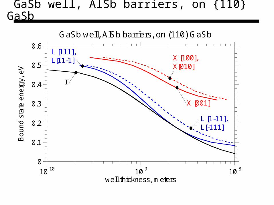
GaSb well, AlSb barriers, on {110} GaSb
0
0.1
0.2
0.3
0.4
0.5
0.6
10-10 10-9 10-8
GaSb well, AlSb barriers, on (110) GaSb
Bo
und
sta
te e
nerg
y, e
V
well thickness, meters
L [111], L[11-1]
L [1-11], L[-111]
X [001]
X [100], X[010]