IEEE TRANSACTIONS ON VERY LARGE SCALE …bxc162630/darclab/publications/TVLSI_temperature...IEEE...
13
IEEE TRANSACTIONS ON VERY LARGE SCALE INTEGRATION (VLSI) SYSTEM CLASS FILES, VOL. 1, NO. 11, DECEMBER 2007 1 Hotspots Elimination and Temperature Flattening in VLSI Circuits Benjamin Carrion Schafer, Member, IEEE and Taewhan Kim, Member, IEEE Abstract— This paper proposes a new solution to the problem of eliminating hotspots from gate-level netlits as well as examines the effects of timing constraints on the temperature reduction and the overall temperature flattening on the chip . Our core technique consists of three steps. First, a thermal analysis is carried out for logic netlists. (The netlists are assumed to be either isolated or embedded in a larger system with macro- cells.) We then apply a new technique, called isothermal logic partitioning technique (LP-temp), to the netlists, which essentially builds isothermal logic clusters for the netlists and splits each of the logic clusters exceeding the maximum allowed temperature through its hottest point. This will enlarge a contact point for the hotspot to cool down. Finally, the entire system is replaced using a custom designed temperature-aware floorplanner so that the temperature across the entire system is reduced and flattened. We have developed a thermal-aware design flow, integrating our thermal-aware logic partitioning technique with a timing and thermal-aware floorplanner. Two cases were analyzed: (tight timing) LP-temp combined with the timing and thermal-aware floorplanner, where the partitioned units by LP-temp are replaced locally considering a tight timing budget (5% timing degra- dation); (loose timing) LP-temp combined with thermal-aware replacement, considering a loose timing budget (10% timing degradation). From experimentations using a set of benchmark designs, it is confirmed that our temperature reduction technique is effective, generating designs with an average of 5.54% and 9.9% more reduction of peak temperature (on average) for the cases of tight and loose timing than that of the designs by a conventional thermal-aware floorplanner without using LP-temp, respectively. We also analyzed the effect of our proposed technique on Field Programmable Gate Arrays(FPGAs) in order to contrast its effectiveness on systems with hotspots on hardmacros. Results show that our technique can reduce the temperature in these systems on average 3.40% and 6.61% for the case of loose and tight timing constraints respectively compared to the thermal- aware floorplanner without using LP-temp. Index Terms—Hotspots, Temperature reduction, Temperature flattening, Leakage power. I. I NTRODUCTION W ITH the implacable technology advent, integrated circuits design is facing new challenges. Smaller size Manuscript received August 29, 2006; revised June 3, 2007. The work was performed while B. Carrion Schafer was a visiting researcher at Seoul National University and has been supported by the Nano IP/SoC Promotion Group of Seoul R&D Program, IT-SoC Program, ETRI project, System IC2010 project of Korea Ministry of Commerce, Industry and Energy, and by the Korea Science and Engineering.Foundation grant funded by the Korea. government(MOST) (No.R01-2007-000-20891-0). B. Carrion Schafer is with NEC Corporation, EDA R&D Center, Kawasaki, Kanagawa 211-8666 Japan (phone: +81 44 435 9486; fax: +81 44 435 9491; e-mail: [email protected]). T.Kim is with Seoul National University, Seoul 151-744, Korea (e-mail: [email protected]). transistors allow higher logic densities but involve also the leakage power is now becoming a significant design factor and is reaching a point where it equals the dynamic power consumed in the chip [1]. Low-K dielectrics, triple-oxides, improved design tools and power efficient architectures have avoid so far the most pessimistic forecasts, but extreme power consuming devices are generating great amounts of heat. State of the art microprocessors like the Intel’s new Itanium processor now incorporate power controllers on the same die [2] and new FPGAs, like Xilinxs Virtex 5 [3] incorporate on-chip power supply and thermal monitoring capabilities. Reducing temperature increase is becoming a major issue of concern for highly integrated circuit designs that should be addressed in the overall design process in order to keep the chip temperature as low as possible [4]. Temperature has an adverse effect on multiple aspects. It affects the lifetime of the integrated circuit by accelerating the chemical process taking place inside of the chip following Arrhenius equation. Studies show the mean time between failure (MTBF) of an IC is multiplied by a factor 10 for every 30 o C rise in the junction temperature [5]. Secondly leakage power is becoming the dominant source of power consumption for new process technologies [1] which grows exponentially with temperature. Moreover, temperature has a negative effect on carrier mobility and therefore switching speed of the transistors and thus the overall timing of the circuit. Specially global signals like the global clock tree suffer increased clock skew [6]. Consequently it is highly desirable to have an even temperature distribution on the chip in order to avoid costly re-design due to timing/temperature and simplify the verification phase. Furthermore, expensive heat dissipaters are required to maintain the chip at a reasonable temperature or could not be used in case of embedded system. Studies have reported that above 30-40 Watts (W), additional power dissipation increases the total cost per chip by more than $1/W [7]. Field-Programmable Gate Arrays (FPGAs) are no excep- tion, especially state of the art FPGAs, like Xilinx’s Virtex5 and Altera’s Stratix III, based on a 65nm design process and 12 copper interconnect layers. The post fabrication flexibility provided by these devices is implemented using a large number of prefabricated routing tracks and programmable switches. These interconnects can be long, and can consume a significant amount of power. In addition, the programmable switches add capacitance to each wire-segment, which further increasing their power dissipation. Finally, the generic logic structures consume more power than the dedicated logic in ASICs. The
Transcript of IEEE TRANSACTIONS ON VERY LARGE SCALE …bxc162630/darclab/publications/TVLSI_temperature...IEEE...

IEEE TRANSACTIONS ON VERY LARGE SCALE INTEGRATION (VLSI) SYSTEM CLASS FILES, VOL. 1, NO. 11, DECEMBER 2007 1
Hotspots Elimination and Temperature Flattening inVLSI Circuits
Benjamin Carrion Schafer, Member, IEEE and Taewhan Kim, Member, IEEE
Abstract— This paper proposes a new solution to the problemof eliminating hotspots from gate-level netlits as well as examinesthe effects of timing constraints on the temperature reductionand the overall temperature flattening on the chip . Our coretechnique consists of three steps. First, a thermal analysis iscarried out for logic netlists. (The netlists are assumed to beeither isolated or embedded in a larger system with macro-cells.) We then apply a new technique, called isothermal logicpartitioning technique (LP-temp), to the netlists, which essentiallybuilds isothermal logic clusters for the netlists and splits each ofthe logic clusters exceeding the maximum allowed temperaturethrough its hottest point. This will enlarge a contact point for thehotspot to cool down. Finally, the entire system is replaced usinga custom designed temperature-aware floorplanner so that thetemperature across the entire system is reduced and flattened.
We have developed a thermal-aware design flow, integratingour thermal-aware logic partitioning technique with a timingand thermal-aware floorplanner. Two cases were analyzed: (tighttiming) LP-temp combined with the timing and thermal-awarefloorplanner, where the partitioned units by LP-temp are replacedlocally considering a tight timing budget (5% timing degra-dation); (loose timing) LP-temp combined with thermal-awarereplacement, considering a loose timing budget (10% timingdegradation). From experimentations using a set of benchmarkdesigns, it is confirmed that our temperature reduction techniqueis effective, generating designs with an average of 5.54% and9.9% more reduction of peak temperature (on average) for thecases of tight and loose timing than that of the designs by aconventional thermal-aware floorplanner without using LP-temp,respectively.
We also analyzed the effect of our proposed technique onField Programmable Gate Arrays(FPGAs) in order to contrastits effectiveness on systems with hotspots on hardmacros. Resultsshow that our technique can reduce the temperature in thesesystems on average 3.40% and 6.61% for the case of loose andtight timing constraints respectively compared to the thermal-aware floorplanner without using LP-temp.
Index Terms— Hotspots, Temperature reduction, Temperatureflattening, Leakage power.
I. INTRODUCTION
W ITH the implacable technology advent, integratedcircuits design is facing new challenges. Smaller size
Manuscript received August 29, 2006; revised June 3, 2007. The workwas performed while B. Carrion Schafer was a visiting researcher at SeoulNational University and has been supported by the Nano IP/SoC PromotionGroup of Seoul R&D Program, IT-SoC Program, ETRI project, SystemIC2010 project of Korea Ministry of Commerce, Industry and Energy, andby the Korea Science and Engineering.Foundation grant funded by the Korea.government(MOST) (No.R01-2007-000-20891-0).
B. Carrion Schafer is with NEC Corporation, EDA R&D Center, Kawasaki,Kanagawa 211-8666 Japan (phone: +81 44 435 9486; fax: +81 44 435 9491;e-mail: [email protected]).
T.Kim is with Seoul National University, Seoul 151-744, Korea (e-mail:[email protected]).
transistors allow higher logic densities but involve also theleakage power is now becoming a significant design factorand is reaching a point where it equals the dynamic powerconsumed in the chip [1]. Low-K dielectrics, triple-oxides,improved design tools and power efficient architectures haveavoid so far the most pessimistic forecasts, but extreme powerconsuming devices are generating great amounts of heat.State of the art microprocessors like the Intel’s new Itaniumprocessor now incorporate power controllers on the same die[2] and new FPGAs, like Xilinxs Virtex 5 [3] incorporateon-chip power supply and thermal monitoring capabilities.Reducing temperature increase is becoming a major issue ofconcern for highly integrated circuit designs that should beaddressed in the overall design process in order to keep thechip temperature as low as possible [4].
Temperature has an adverse effect on multiple aspects. Itaffects the lifetime of the integrated circuit by acceleratingthe chemical process taking place inside of the chip followingArrhenius equation. Studies show the mean time betweenfailure (MTBF) of an IC is multiplied by a factor 10 forevery 30oC rise in the junction temperature [5]. Secondlyleakage power is becoming the dominant source of powerconsumption for new process technologies [1] which growsexponentially with temperature. Moreover, temperature has anegative effect on carrier mobility and therefore switchingspeed of the transistors and thus the overall timing of thecircuit. Specially global signals like the global clock tree sufferincreased clock skew [6]. Consequently it is highly desirableto have an even temperature distribution on the chip in order toavoid costly re-design due to timing/temperature and simplifythe verification phase. Furthermore, expensive heat dissipatersare required to maintain the chip at a reasonable temperatureor could not be used in case of embedded system. Studieshave reported that above 30-40 Watts (W), additional powerdissipation increases the total cost per chip by more than $1/W[7].
Field-Programmable Gate Arrays (FPGAs) are no excep-tion, especially state of the art FPGAs, like Xilinx’s Virtex5and Altera’s Stratix III, based on a 65nm design process and12 copper interconnect layers. The post fabrication flexibilityprovided by these devices is implemented using a large numberof prefabricated routing tracks and programmable switches.These interconnects can be long, and can consume a significantamount of power. In addition, the programmable switches addcapacitance to each wire-segment, which further increasingtheir power dissipation. Finally, the generic logic structuresconsume more power than the dedicated logic in ASICs. The

IEEE TRANSACTIONS ON VERY LARGE SCALE INTEGRATION (VLSI) SYSTEM CLASS FILES, VOL. 1, NO. 11, DECEMBER 2007 2
power consumed by the FPGA will lead to heat generationand in turn to the rising of the overall die temperature. Thisunderlines again the importance of embedding temperaturereduction techniques in the main design flow.
Temperature is highly dependent on power consumption butdepends on a multiple of other factors, making power alonenot a valid measure for temperature. Temperature also dependson the placement of the units in the chip. Placing heavy powerconsuming units close together will intuitively generate aneven higher temperature area in the chip as temperature isadditive in nature. In contrast, placing power consuming unitsclose to units that have a moderate power consumption willallow the heat generated to dissipate through these units. Otheraspects that affect temperature are the execution order of tasksin a unit. Executing tasks one after the other will help thetemperature build up whereas spacing the execution of tasksin a unit will allow the unit to have a time to prevent it fromheating up. Consequently, temperature should be addressed asan individual design parameter.
Temperature affects many different aspects of the chipand therefore covers multiple research areas. Techniques toimprove the heat removal capabilities as well as design ofpackages and heat sinks have been developed in [8]. At thetaks/processor level, runtime thermal management techniqueshave been developed such as clock gating using real-timetemperature sensors [9] or at the compilation level assigninginstructions to the coolest available functional unit in VLIWprocessors [10]. Furthermore, lowering temperature downthrough power saving techniques such as dynamic voltagescaling (DVS) and sub-banking has been investigated in [11],[12], [13]. On the other hand, in the architectural level,temperature flattening on SoCs by partitioning modules andusing the embedded memory as cooling components has beenstudied in [14]. Resource allocation and binding at high levelsynthesis stage has been addressed recently in [15] as well asthermal-aware floorplanners in [16], [17].
To the best of our knowledge so far, it has not beenattempted to deal with the temperature reduction at the gatelevel, where a temperature profile of the given netlist isobtained and the temperature inside the given netlist is reducedby recursive partitions of the netlist and re-placements of theresultant units under a timing budget constraint. Working atthe gate level has the advantage that extremely accurate powervalues are obtained as well as exact placement information sothat temperature reduction can be accurately tackled. Otherapproaches at higher levels of abstractions consider a uniformpower distribution of each unit, which does not happen inreality (e.g. in a multiplier if small numbers are permanentlymultiplied the gates corresponding to the lower bits will beswitched more often then the gates corresponding to the higherbit ). The contributions of this work can be summarized asfollows:• Analyzes gate-level netlists and generates a thermal map
of the netlists. We allow the designer to specify thegranularity of the temperature map. The thermal mapwill provide a global view of temperature distribution,in addition to the locations of hotspots, coolspots as wellas the thermal distribution in the chip.
• Introduces a thermal-aware logic partitioning technique,called isothermal logic partitioning (LP-temp), whicheffectively weakens the hotspots and distributes the tem-perature evenly for custom logic design as well as forFPGAs.
• Proposes a thermal-aware design flow of logic partition-ing and placement. A set of comprehensive comparisonsbetween the proposed design flow and the conventionalthermal-aware flow is given for custom VLSI design aswell as for FPGAs.
• Studies the importance of timing budget on temperaturereduction as well as on overall temperature flatting con-sidering designs with gate netlists as well as systems withmixed gate netlists and hardmacros.
• Extends previous work on synthetic benchmarks to incor-porate state of the art FPGA hardmacros like embeddedmultipliers and embedded memories.
This work is made on the assumption that heat flowslaterally inside the chip, as shown in multiple previous works,especially thermal-aware floorplanners [18], [19], [20]. Theinfluence of the lateral heat flow will depend on the thermalconductivity of the primary and secondary heat flows of thechip (heat flow through the package and through the pinsrespectively). In this case we are targeting mostly embeddedsystems, which have very strict space constraints limiting thetype and size of the heatsink. In these cases lateral heat flowbecomes extremely important. On the other hand being ableto control the lateral heat flow allows also to use a cheaperpackage (with lower conductivity).
The paper is organized as follows. Section II shows a moti-vational example to illustrate what the limitations of previousthermal-aware placement method are, and how they can beovercome by logic partitioning. Then, in subsection III.A thethermal simulation method we developed is described followedby details on the procedure of our core technique, isothermallogic partitioning, in subsection III.B. A complete frameworkcombining the isothermal logic partitioning technique withthermal-aware floorplanners is then covered in subsectionIII.C. Section IV provides a set of experimental results toshow the effectiveness of our approach. Finally, section Vgives concluding remarks.
II. MOTIVATIONAL EXAMPLE
When trying to eliminate hotspots or flattening the overallchip temperature, the previous thermal-aware floorplannersassumed that each unit to be placed has an ‘even’ temperaturedistribution. For example, suppose the floorplan in Fig. 1(a)is the one with the best timing. When we perform a thermal-aware floorplanning without considering logic partitioning, theresultant floorplan will look like the one in Fig. 1(b) wherethe two cool units Unit3 and Unit4 with temperature of 40oCsurround the hot unit Unit1 to take heat from it, conservingthe timing constraint. This result occurs because the thermal-aware floorplanner places units so that the heat flow in thechip is to be maximized allowing hotter units to cool downfaster by placing them close to cooler ones. This can be agood way to flatten the overall chip temperature (at a coarse

IEEE TRANSACTIONS ON VERY LARGE SCALE INTEGRATION (VLSI) SYSTEM CLASS FILES, VOL. 1, NO. 11, DECEMBER 2007 3
level), but is not a viable way to reduce the appearance ofhotspots as a hotspot can happen in the middle of a unit.In this case where a hotspot appears in the center part of aunit, no previously known methods without logic partitioningseem to eliminate its appearance. We can see, in Unit 1 ofFig. 1(b), the appearance of a hotspot because the unit is toobig to be completely cooled down by Unit3 and Unit4. Onthe other hand, Fig. 1(c) shows a resultant floorplan for Unitsafter partitioning it into three pieces and replacement allowingonly a small timing degradation. Since a clever partition withre-placement may reduce the possible concentration of heatflow, the hotspot would be small in size compared to that inFig. 1(a).
Fig. 1. Motivational example to illustrate the effects of logic partitioing onchip temperature.
Fig. 1(d) show a resultant floorplan which can be obtainedby exploiting both of the logic partitioning of Unit1 anda wider replacement, allowing a higher timing degradation.Since in this case, the partitioned units can be relocated ina wider range of ‘good’ places, the temperature could befurther reduced below the limit (i.e., no hotspot as indicatedin Fig. 1(d)). The example shown in Fig. 1 illustrates thatto weaken the hotspots, logic partition can play an importantrole, and its effectiveness can be greatly expanded if a thermal-aware replacement and a (thermal-aware) logic partitioning aretightly combined.
Note that the conventional thermal-aware floorplanner withno logic partitioning usually uses a coarse grained (e.g.,architectural modules, blocks) power information for everyunit in the design. This simplifies the power estimation aswell as the thermal simulation of the system. However, if alogic partitioning is taken into account, a more elaborated finegrained thermal estimation technique is required because some
SelectRAM Blocks
Embedded DSP blocks
2CLB column
2CLB column
2CLB column
2CLB column
n CLB column
n CLB column
Fig. 2. Simplified Xilinx VirtexII floorplan.
parts in a unit might get hotter than others due to the differenceof intrinsic switching activity of their transistors.
The same technique can be applied to FPGAs. The onlyaspects to be considered are the embedded hardmacros asshown on Fig. 2 as well a its particular floorplan structure.We will use FPGAs to validate our technique on systems withhardmacros, as shown on the experimental section.
III. TEMPERATURE-AWARE LOGIC PARTITIONING ANDPLACEMENT
Our work consists of three parts: (part 1) development oftemperature simulator to generate a thermal map, (part 2) gen-erating a thermal map from the data in part 1 and performinga thermal-aware logic partitioning, LP-temp, based on thethermal map, and (part 3) building a complete framework thatcombines LP-temp with thermal-aware floorplanner. The threeparts are described in detail in the following three subsections.
A. Temperature Simulator
In order to have a consistent thermal-aware design flow, asuitable thermal model is needed. On one side it should beaccurate enough and on the other side it should be compu-tationally efficient. The thermal model used in this case isbased on the known duality between electricity and thermalflow [21] and is based on the model developed by Skadron,et al. [22]. Some changes are made from their model as theyonly consider one type of package (CBGA) with a specificheat sink. In our model, the user can choose a package from alibrary of different packages so that the equivalent thermalmodel is generated according to the chosen package. Theprimary and secondary heat flows will depend on the packagetype selected. In case of a CBGA package, the primary flowwill dissipate heat through the heat sink and the secondaryflow will propagate heat through pins of the chip to the PCB.
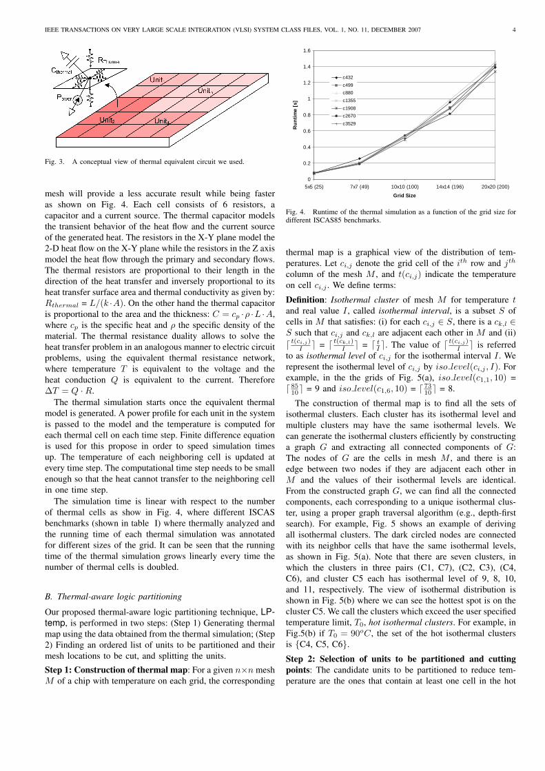
A thermal mesh is generated on top of the given floorplan, asshown in Fig. 3. The size of each thermal cell is establishedby the user. A finer mesh will yield a more precise resultwhile taking a longer computational time, whereas a coarser
IEEE TRANSACTIONS ON VERY LARGE SCALE INTEGRATION (VLSI) SYSTEM CLASS FILES, VOL. 1, NO. 11, DECEMBER 2007 4
Fig. 3. A conceptual view of thermal equivalent circuit we used.
mesh will provide a less accurate result while being fasteras shown on Fig. 4. Each cell consists of 6 resistors, acapacitor and a current source. The thermal capacitor modelsthe transient behavior of the heat flow and the current sourceof the generated heat. The resistors in the X-Y plane model the2-D heat flow on the X-Y plane while the resistors in the Z axismodel the heat flow through the primary and secondary flows.The thermal resistors are proportional to their length in thedirection of the heat transfer and inversely proportional to itsheat transfer surface area and thermal conductivity as given by:Rthermal = L/(k ·A). On the other hand the thermal capacitoris proportional to the area and the thickness: C = cp ·ρ ·L ·A,where cp is the specific heat and ρ the specific density of thematerial. The thermal resistance duality allows to solve theheat transfer problem in an analogous manner to electric circuitproblems, using the equivalent thermal resistance network,where temperature T is equivalent to the voltage and theheat conduction Q is equivalent to the current. Therefore∆T = Q ·R.
The thermal simulation starts once the equivalent thermalmodel is generated. A power profile for each unit in the systemis passed to the model and the temperature is computed foreach thermal cell on each time step. Finite difference equationis used for this propose in order to speed simulation timesup. The temperature of each neighboring cell is updated atevery time step. The computational time step needs to be smallenough so that the heat cannot transfer to the neighboring cellin one time step.
The simulation time is linear with respect to the numberof thermal cells as show in Fig. 4, where different ISCASbenchmarks (shown in table I) where thermally analyzed andthe running time of each thermal simulation was annotatedfor different sizes of the grid. It can be seen that the runningtime of the thermal simulation grows linearly every time thenumber of thermal cells is doubled.
B. Thermal-aware logic partitioning
Our proposed thermal-aware logic partitioning technique, LP-temp, is performed in two steps: (Step 1) Generating thermalmap using the data obtained from the thermal simulation; (Step2) Finding an ordered list of units to be partitioned and theirmesh locations to be cut, and splitting the units.
Step 1: Construction of thermal map: For a given n×n meshM of a chip with temperature on each grid, the corresponding
0
0.2
0.4
0.6
0.8
1
1.2
1.4
1.6
5x5 (25) 7x7 (49) 10x10 (100) 14x14 (196) 20x20 (200)
Grid Size
Ru
nti
me
[s]
c432
c499
c880
c1355
c1908
c2670
c3529
Fig. 4. Runtime of the thermal simulation as a function of the grid size fordifferent ISCAS85 benchmarks.
thermal map is a graphical view of the distribution of tem-peratures. Let ci,j denote the grid cell of the ith row and jth
column of the mesh M , and t(ci,j) indicate the temperatureon cell ci,j . We define terms:
Definition: Isothermal cluster of mesh M for temperature tand real value I , called isothermal interval, is a subset S ofcells in M that satisfies: (i) for each ci,j ∈ S, there is a ck,l ∈S such that ci,j and ck,l are adjacent each other in M and (ii)d t(ci,j)
I e = d t(ck,l)I e = d t
I e. The value of d t(ci,j)I e is referred
to as isothermal level of ci,j for the isothermal interval I . Werepresent the isothermal level of ci,j by iso level(ci,j , I). Forexample, in the the grids of Fig. 5(a), iso level(c1,1, 10) =d 85
10e = 9 and iso level(c1,6, 10) = d 7310e = 8.
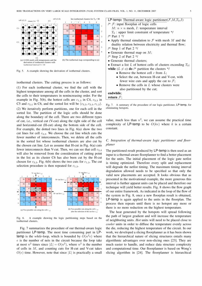
The construction of thermal map is to find all the sets ofisothermal clusters. Each cluster has its isothermal level andmultiple clusters may have the same isothermal levels. Wecan generate the isothermal clusters efficiently by constructinga graph G and extracting all connected components of G:The nodes of G are the cells in mesh M , and there is anedge between two nodes if they are adjacent each other inM and the values of their isothermal levels are identical.From the constructed graph G, we can find all the connectedcomponents, each corresponding to a unique isothermal clus-ter, using a proper graph traversal algorithm (e.g., depth-firstsearch). For example, Fig. 5 shows an example of derivingall isothermal clusters. The dark circled nodes are connectedwith its neighbor cells that have the same isothermal levels,as shown in Fig. 5(a). Note that there are seven clusters, inwhich the clusters in three pairs (C1, C7), (C2, C3), (C4,C6), and cluster C5 each has isothermal level of 9, 8, 10,and 11, respectively. The view of isothermal distribution isshown in Fig. 5(b) where we can see the hottest spot is on thecluster C5. We call the clusters which exceed the user specifiedtemperature limit, T0, hot isothermal clusters. For example, inFig.5(b) if T0 = 90oC, the set of the hot isothermal clustersis {C4, C5, C6}.
Step 2: Selection of units to be partitioned and cuttingpoints: The candidate units to be partitioned to reduce tem-perature are the ones that contain at least one cell in the hot
IEEE TRANSACTIONS ON VERY LARGE SCALE INTEGRATION (VLSI) SYSTEM CLASS FILES, VOL. 1, NO. 11, DECEMBER 2007 5
96 8588
84 86
78 78
C6(a) A 6X6 mesh with temperatures and the derivation of isothermal clusters with isothermal interval I = 10
(b) The isothermal map correponding to (a)
85
85
84
78
79
78
75 76
78
86
87
86
91 93
112
118
111
97
79
76
115
100
98
96
91
75
113
115
95
88
92
73
78
83
84
89
C1
C2
C7
C5 C3
85
78
79
75 76
86
87
91 93
112
118
111
97
79
76
115
100
98
91
75
113
115
95
73
78
83
84
92 89
hot isothermal clusters for T = 900
1
2
3
4
5
6
1 2 4 5 63
96
cell c(1,1)cell c(1,6)
cluster C4
Fig. 5. A example showing the derivation of isothermal clusters.
isothermal clusters. The cutting process is as follows:(1) For each isothermal cluster, we find the cell with thehighest temperature among all the cells in the cluster, and sortthe cells to their temperatures in nonincreasing order. For theexample in Fig. 5(b), the hottest cells are c1,3 in C4, c3,3 inC5 and c3,4 in C6, and the sorted list will be (c3,3, c3,4, c1,3).(2) We iteratively perform partitions, one for each cell in thesorted list. The partition of the logic cells should be donealong the boundary of the cell. There are two different typesof cut, i.e., vertical cut (V-cut) along the right side of the celland horizontal-cut (H-cut) along the bottom side of the cell.For example, the dotted two lines in Fig. 6(a) show the twocut lines for cell c3,3. We choose the cut line which cuts thefewer number of interconnects. Then, we delete all the cellsin the sorted list whose isothermal clusters are also cut bythe chosen cut line. Let us assume that H-cut in Fig. 6(a) cutsfewer interconnects than V-cut. Then, we can see that cell c3,4
will also be removed from the consideration of cutting pointin the list as its cluster C6 has also been cut by the H-cutchosen for c3,3. Fig. 6(b) shows the two cuts for c1,3. The cutselection procedure is then repeated for c1,3.
H−cut for c3,3
H−cut for c1,31
2
3
4
5
6
85
78
79
75 76
86
87
91 93
112
118
111
97
79
76
115
100
98
91
75
113
115
95
73
78
83
84
92 89
1
2
3
4
5
6
1 2 4 5 63
9678 78 8588
84 86
V−cut for c1,4
85
78
79
75 76
86
87
91 93
112
111
97
79
76
115
98
91
75
113
115
95
73
78
83
84
92 89
1 2 4 5 63
9678 78 8588
84 86
3,3V−cut for c
1,4
after the selection of the cut for c(a) Two possible cuts along the cell c3,3
3,3
(b) Two possible cuts along the cell c
100118
Fig. 6. A example showing the logic partitioning steps based on theisothermal clusters.
Fig. 7 summarizes the procedure of our thermal-aware logicpartitioner LP-temp. The most time consuming part in LP-temp is the while-loop, which is bounded by O(n2e) wheree is the number of nets in the circuit because the loop takeat most n2 times since |L| = O(n2), where n2 is the numberof cells in M , and counting cuts for H-cut and V-cut takesO(e) time. However, note that since |L| is practically a small
LP-temp: Thermal-aware logic partitioner(F ,M ,T0,I)/* F : input floorplan of logic cells
M : n× n mesh, I: temperature intervalT0 : upper limit constraint of temperature */
/* Part 1 */• Apply thermal simulation to F with mesh M and the
duality relation between electricity and thermal flow;/* Step 1 of Part 2 */• Generate thermal map on M ;/* Step 2 of Part 2 */• Generate thermal clusters;• Extract a list L of hottest cells of clusters exceeding T0;while (L 6= ø) do /* partition the clusters */
• Remove the hottest cell c from L;• Select the cut, between H-cut and V-cut, with
fewer wire cuts and apply the cut to F ;• Remove the cells in L whose clusters were
also partitioned by the cut;endwhile;return F ;
Fig. 7. A summary of the procedure of our logic partitioner, LP-temp, foreliminating hotspots.
value, much less than n2, we can assume the practical timecomplexity of LP-temp to be O(ke) where k is a certainconstant.
C. Integration of thermal-aware logic partitioner and floor-planer
The partitioned result produced by LP-temp is then used as aninput to a thermal-aware floorplanner to find a better placementfor the units. The initial placement of the logic gate netlistis timing optimized. Therefore every split and replacementwill degrade the netlist timing. The maximum timing intervaldegradation allowed needs to be specified so that only thevalid new placements are accepted. It looks obvious that aspresented in the motivational example, the more generous thisinterval is further apparat units can be placed and therefore ourtechnique will yield better results. Fig. 8 shows the flow graphof our entire framework. As indicated in the loop of the flow ofthe system in Fig. 8, once a new floorplan result is obtained,LP-temp is again applied to the units in the floorplan. Theprocess then repeats until there is no hotspot any more orthere is no more reduction on the highest temperature.
The heat generated by the hotspots will spread followingthe path of largest gradient and will increase the temperatureof neighboring units. Hot units will need to be placed close tocooler units in order to diffuse the temperature evenly acrossthe die, reducing the highest temperature of the circuit. In ourwork, we developed a slicing floorplanner as it has been shownthat the hierarchical nature of slicing structures entails manyalgorithmic advantages over non-slicing ones [23]. They aremuch easier to handle, and reduce data structure complexityand computational time. Our floorplanner is based on Wong’sslicing algorithm in [24]. The floorplanner is hierarchical

IEEE TRANSACTIONS ON VERY LARGE SCALE INTEGRATION (VLSI) SYSTEM CLASS FILES, VOL. 1, NO. 11, DECEMBER 2007 6
Thermal simulation
Generate thermal map
Hotspots
found?
“Split” unit V or H through hotspot(s)
(min congestion cut)
Timing and thermal-Aware
Floorplanner
Exit
Y
N
Power estimatorInput
stimuli
Max timing
degrdation
allowed
Floorplan with units built out of gate netlists
and black boxes
Fig. 8. The entire flow of our proposed framework.
allowing a top unit to be built of multiple units and/or a gate-level netlist.
The cost function of the simulated annealing floorplanneris given by COST = αA + βW + γT . The weighting factorsα, β, γ can be modified in order to represent the importanceof minimizing the total area A), wire length(W), or maximaltemperature(T). In order to place cooler units close to hotterones, the cost function was modified in order to maximize theheat diffusion between two adjacent blocks (D). Specifically,heat diffusion is proportional to the temperature differenceand the length of their contact area [25]. The cost functionredefined is COST = αA + βW − γD, in order to considerthe heat diffusion as one of its parameters. D has a negativesign as we want to maximize the heat diffusion. In our case aswe are analyzing the effects of the floorplan on temperaturewe chose the thermal diffusion coefficient (γ) twice as largeas the area (α) and wire length (β) one.
IV. EXPERIMENTAL RESULTS
First, we describe the experimental setup for the generation ofinitial floorplans for custom logic designs of the conventionaland our proposed thermal-aware design flow here investigated.Then, we show a set of comprehensive results obtained, to-gether with explanations on the implication and analysis of thedata. Secondly we apply our methodology to FPGAs showinghow our temperature reduction and flattening technique canalso be effective on FPGAs with multiple hotspots (some onthe logic and some on hardmacros).
A. Experimental Setup for Custom Logic
To test our temperature reduction flow, we have developedour own integrated environment in C++. This tool (that wecall hotkiller) has a main program with multiple external
subroutines (libraries) that are called upon needed. The li-braries correspond to the major steps in the flow, which arethe power estimator, thermal-aware floorplanner, thermal sim-ulator, thermal-aware partitioner and a synthetic benchmarkgenerator (used for the FPGA benchmarks) as shown on Fig9. The tool has a set of libraries as inputs so that either acustom floorplan can be specified or one from the libraries canbe chosen. Libraries include a set of Xilinx FPGAs. The outputof the design flow will be a temperature optimized design.
TABLE ITYPES AND SIZES OF TESTED BENCHMARKS BASED ON THE ISCAS85
BENCHMARK CIRCUITS
Benchmark Netlists (gates) # Total GatesBench 1 c432, c499, c880, c1355 1291
(160,202,383,546)Bench 2 c499, c880, c1355, c1908 2011
(202,383,546, 880)Bench 3 c880, c1355, c1908, c2670 3078
(383,546, 880,1269 )Bench 4 c880, c1908, c2670, c3529 4201
(383,880,1269,1669 )Bench 5 c1355, c1908, c2670, c3529 4364
(546,880, 1269, 1669 )Bench 6 c1355, c1908, c2670, c5315 5002
(546,880, 1269,2307)Bench 7 c1908, c2670, c3529, c5315 6125
(880, 1269, 1669,2307)Bench 8 c1355, c2670, c3529, c6288 5900
(546, 1269, 1669, 2416)Bench 9 c1355, c2670, c5315, c7522 7634
(546, 1269, 1669,3512)Bench 10 2670, c5315, c6288, c7522 9504
(1269, 1669, 2416,3512)
To test the effectiveness of our proposed design flow inte-grated with logic partitioner LP-temp, we generate a randomfloorplan with 4 different gate netlists assigned to each unitin the floorplan for all cases as shown in Fig.10. The testedcircuits are taken from the ISCAS85 benchmarks and have atotal combined size that range between 1291 to 9505 gates, as
Fig. 9. Hotkiller tool block diagram.

IEEE TRANSACTIONS ON VERY LARGE SCALE INTEGRATION (VLSI) SYSTEM CLASS FILES, VOL. 1, NO. 11, DECEMBER 2007 7
TABLE IIA COMPARISON OF PEAK TEMPERATURES PRODUCED BY THE CONVENTIONAL THERMAL-AWARE FLOORPLANNER AND OUR THERMAL-AWARE LOGIC
PARTITIONER.
Thermal-aware floorplan only LP-temp + 5% timing floorplan LP-temp + 10% timing floorplanTinit Tpeak ∆T[oC] ∆T[%] Tpeak ∆T[oC] ∆T[%] # Tpeak ∆T[oC] ∆T[%] #
Bench 1 64.71 60.32 4.39 6.78 58.54 6.17 9.53 10 55.67 9.04 13.97 8Bench 2 66.38 62.22 4.16 6.27 59.68 6.7 10.09 8 56.64 9.74 14.67 8Bench 3 64.98 59.23 5.75 8.85 57.31 7.67 11.80 9 55.91 9.07 13.96 8Bench 4 65.65 62.56 3.09 4.71 57.91 7.74 11.79 8 55.81 9.84 14.99 8Bench 5 66.89 62.57 4.32 6.46 60.31 6.58 9.84 9 57.52 9.37 14.01 9Bench 6 67.23 63.84 3.39 5.04 61.75 5.48 8.15 8 57.62 9.61 14.29 10Bench 7 67.89 65.64 2.25 3.31 59.94 7.95 11.71 9 59.19 8.7 12.81 9Bench 8 69.41 66.37 3.04 4.38 61.84 7.57 10.91 10 59.74 9.67 13.93 11Bench 9 71.23 69.01 2.22 3.12 63.31 7.92 11.12 11 62.4 8.83 12.40 12
Bench 10 70.81 69.11 1.7 2.40 62.46 8.35 11.79 12 59.97 10.84 15.31 12Avg 67.51 64.09 3.43 5.13 60.31 7.21 10.67 9 58.05 9.47 14.03 9
c432
Highswitchingactivity
c880
Mediumswitchingactivity
c1355
Lowswitchingactivity
c499
Lowswitchingactivity
Bechmark 1
Fig. 10. Benchmark 1 floorplan example
shown in table I. An input stimuli file with different switchingactivities is generated with 10,000 input values and assigned toeach gatenetlist. Then, the switching activity is simulated usingthe embedded power estimator computing the capacitances foreach gate based on [26]. To achieve a thermal gradient in thechip different netlists are assigned different types of stimulifiles in order to have one with a high switching activity, onewith a medium switching activity and the last two with lowswitching activity as shown on Fig.10, where a 4 unit floorplanis shown with 4 different netlist assigned to each unit each withdifferent switching activity.
We then generated three different solutions by applyingthe following three approaches. The first one is the thermal-aware floorplanning without logic partitioning (thermal-aware floorplan only in Table II). This solution will place theunits thermally as convenient as possible, placing cooler unitsnear to hotter ones. The second as well as the third solutionsuse our logic partitioner LP-temp, allowing different levels oftiming degradation (5% and 10%).
B. Experimental Results for Custom Logic
Table II shows a comparison of peak temperatures used by theconventional floorplanner, our logic partitioner with replace-ment allowing up to 5% and 10% of timing degradation. Tinit
in the second column of the table represents the maximum
temperature at the initial floorplan of the corresponding cir-cuits without logic partition. On the other hand, Tpeak at the3rd, 6th, and 10th columns indicates the final peak temperatureused by the corresponding three design flows, respectively. Forthermal-aware floorplans + thermal-aware logic partition, the total number of units produced by LP-temp is alsorecorded in the columns marked with ‘#’. ∆T [oC] and ∆T [%]columns represent the amounts of the peak temperature reduc-tions in [oC] and [%] by applying the corresponding designflows to the initial floorplans of circuits. From the the table,we can see that thermal-aware floorplan only achieves insome cases a good temperature reductions. For example, forsmall circuits (e.g. Bench 1 to Bench 3) the thermal-awarefloorplanner was able to reduce the maximum temperaturebetween 6.27% to 8.85%. For larger circuits (Bench 4 to Bench10) it could only reduce the temperature between of 2.4% to6.46%. The worst results are obtained for large sized circuitswhere the hotspot is located almost at the center of the unit. Inthis case, the floorplanner takes hard time to reduce the hotspottemperature as the cooler units will have no influence on it(e.g. Bench 9 and Bench 10), while our technique consistentlyreduces the temperature of any benchmark independently ofits size by an average of 10.67% and 14.03% for the 5% and10% timing degradation respectively.
Fig. 11 shows how the peak temperature is reduced at everyiteration for both of our thermal-aware design flows, comparedwith the conventional flow, i.e., thermal-aware floorplanneronly. It can be seen that the temperature is reduced until the3rd iteration. At this point, no further cuts were performedas the temperature reduction would be minimal, which meansat the point, our design flows would not yield any furthersignificant temperature reduction.
Fig. 12 shows how the leakage power is reduced at eachbenchmark for the different experimental setups as well as theaverage leakage power savings, considering a 65nm processtechnology, according to the calculations in [26]. It clearlyshows the impact of temperature on leakage power, as leakagepower grows exponentially with temperature.
Figs. 14 and 13 also shows how other metrics (like totalwirelength and maximum delay) behave for the different tech-

IEEE TRANSACTIONS ON VERY LARGE SCALE INTEGRATION (VLSI) SYSTEM CLASS FILES, VOL. 1, NO. 11, DECEMBER 2007 8
40.00
45.00
50.00
55.00
60.00
65.00
70.00
0 1 2 3
Iteration
Tem
p m
ax [C
]
Floorplan-only
LP-temp w ith 5% timing
LP-temp w ith 10% timing
Fig. 11. Average temperature reduction by each of the temperature reductionapproaches after each iteration.
0.00
0.10
0.20
0.30
0.40
0.50
0.60
0.70
0.80
0.90
1.00
1.10
Bench 1
Bench 2
Bench 3
Bench 4
Bench 5
Bench 6
Bench 7
Bench 8
Bench 9
Bench 10 Avg
Pow
er L
eakg
e (%
)
Floorplan-only LP-temp with 5% timing LP-temp with 10% timing
Fig. 12. Average Leakage powers for all three hotspot types by each of thetemperature reduction approaches.
niques. Fig. 13 shows the maximum delay for each benchmark.Though the maximum allowed timing variation is 5% and 10%the average timing penalty is between 3.83% for the case wereup to 5% of timing degradation was allowed and 8.12% forthe 10% case. A timing degradation of 10% was allowed tothethermal-aware floorplan.
Fig. 14 shows the total maximum wirelength of eachbenchmark. It can be noticed that the average wirelengthincreases for the looser timing budget (10% timing) as unitsare now allowed to be placed further away.
In terms of run time, our floorplanner used in each of thethree design flows dominates the run time since it has toperform a thermal simulation in each new annealing step. Theisothermal clustering and logic partitioning take around 3%of the total run time (ran on a Pentium IV at 3.0 GHz with
1,00
1,02
1,04
1,06
1,08
1,10
1,12
Bench
1
Bench
2
Bench
3
Bench
4
Bench
5
Bench
6
Bench
7
Bench
8
Bench
9
Bench
10 Avg
Max
. Del
ay
Floorplan only LP-temp with 5% timing LP-temp with 10% timing
Fig. 13. Maximum critical path delay by each of the temperature reductionapproaches.
0,00
0,20
0,40
0,60
0,80
1,00
1,20
1,40
1,60
Bench1
Bench
2
Bench
3
Bench
4
Bench
5
Bench6
Bench7
Bench8
Bench9
Bench
10Avg
Wire
leng
th [%
]
Floorplan-only LP-temp with 5% timing LP-temp with 10% timing
Fig. 14. Total Wirelength for all three hotspot types by each of thetemperature reduction approaches.
1 GByte of RAM) Run time rises for larger benchmarks asthe thermal simulation also takes longer as well as with thenumber of newly generated units after each split (#)..
Finally Fig. 15 shows the thermal distribution on the diefor Bench 4 for the different techniques. Fig. 15(a)shows theinitial thermal map of the chip and its floorplan on the x-yplane. The temperature is extremely low on units 2-4 as theirswitching activity is relatively low. In contrast Unit 1 has apeak at temperature 65.65oC. Fig. 15(b) shows the thermaldistribution after the thermal-aware floorplanner has been ran.On the x-y plane it can be noticed how Unit 1 is now partiallysurrounded by the colder units allowing it to dissipate part ofits heat through them. The peak temperature is reduced to62.22o but the thermal gradient on the chip is still noticeable.The rest of the cases, show the thermal distribution on the chipafter applying LP-temp using the different timing constraints.Fig. 15(c) shows the 5% increase from the maximum delay,Fig. 15(d) up to 10%, while Fig. 15(e) does not considertiming at all. It can be clearly seen how the temperature isreduced the most for the latter case as well as the temperatureis flattened the most across the chip. Not considering anytiming constraints will allow each unit to be placed anywhereon the chip resulting in a higher temperature reduction andfurthermore total lower temperature gradient. In the case ofonly 5% timing, Fig. 15(c) clearly shows some isolatedtemperature peaks very close to each other, indicating thatthe single generated hotspot is split in multiple smaller onesreducing therefore the peak temperature. On the other hand athe loose timing constraints imposed in Fig. 15(d) allow thepartitioned units to be re-placed further away of each otherreducing the peak temperature further, placing cooler units inbetween hotter ones reducing at the same time the temperaturegradient in the chip, evening the temperatures even further.
C. Experimental Setup for FPGAs
In this section we validate our temperature reduction andflattening technique on state of the art FPGAs with hard-macros. In order to perform the tests on FPGAs suitablebenchmarks were needed. One option would have been to takethe ISCAS benchmarks and map these to an FPGA using [28].This would ensure the use of some real benchmarks, but hasthe drawback that these benchmarks were not designed forFPGAs and therefore do not reflect real needs in FPGA designs

IEEE TRANSACTIONS ON VERY LARGE SCALE INTEGRATION (VLSI) SYSTEM CLASS FILES, VOL. 1, NO. 11, DECEMBER 2007 9
1 3 5 7 9 11 13 15S1
S5
S9
S13
0
10
20
30
40
50
60
70
80
Temperature[C]
70-80
60-70
50-60
40-50
30-40
20-30
10-20
0-10
Unit 1
Unit 2
Unit 4
Unit 3
1 3 5 7 9 11 13 15S1
S6
S11
0
10
20
30
40
50
60
70
Temperature[C]
60-70
50-60
40-50
30-40
20-30
10-20
0-10Unit 1
Unit 2
Unit 4
Unit 3
(a) Initial on-chip thermal distribution (b) Thermal distribution after thermal-aware floorplanner is executed
1 3 5 7 9 11 13 15S1
S6
S11
0
10
20
30
40
50
60
70
Temperature[C]
60-70
50-60
40-50
30-40
20-30
10-20
0-10Unit 2
Unit 3 Unit 4
Unit 1_0
Unit 1_1Unit 1_2
Unit 1_3Unit 1_4
Unit 1_5Unit 1_6
1 3 5 7 9 11 13 15
S1
S5
S9
S13
0
10
20
30
40
50
60
Temperature[C]
50-60
40-50
30-40
20-30
10-20
0-10
Unit 2Unit 3 Unit 4
Unit 1_0Unit 1_1
Unit 1_6
Unit 1_2
Unit 1_3 Unit 1_4Unit 1_5
(c) Thermal distribution after LP-temp with 5% timing constraint is executed (d) Thermal distribution after LP-temp with 10% timing constraint is executed
1 3 5 7 9 11 13 15S1
S5
S9
S13
0
10
20
30
40
50
60
Temperature[C]
50-60
40-50
30-40
20-30
10-20
0-10
Unit 2Unit 3
Unit 4
Unit 1_0
Unit 1_1
Unit 1_2Unit 1_3
Unit 1_4Unit 1_5
(e) Thermal distribution after LP-temp with no timing constraint is executed
Fig. 15. On-chip thermal distributions for the techniques for benchmark4.
and do not consider their hardmacros, which is one of theaspects we want to investigate in this section. For instance theISCAS85 benchmark circuits were developed specifically forthe evaluation of ATPG (Automatic Test Pattern Generation)tools.
We therefore decided to use synthetic benchmarks for ourexperimental results. These present multiple advantages overreal benchmarks. First of all as many benchmarks as needed
can be generated automatically. Secondly, they provide fullcontrol over the benchmark’s most important characteristicparameters, such as circuit size, interconnection structure andfunctionality. The main advantage is the controllability of asingle characteristic parameter at a time. The major drawbackof synthetic benchmarks is that it is hard to prove that theyare equivalent to certain real benchmarks.
IEEE TRANSACTIONS ON VERY LARGE SCALE INTEGRATION (VLSI) SYSTEM CLASS FILES, VOL. 1, NO. 11, DECEMBER 2007 10
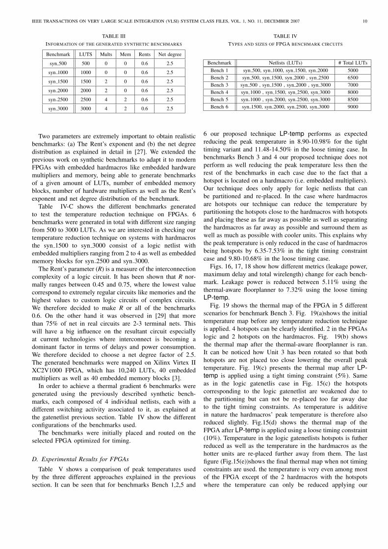
TABLE IIIINFORMATION OF THE GENERATED SYNTHETIC BENCHMARKS
Benchmark LUTS Mults Mem Rents Net degree
syn 500 500 0 0 0.6 2.5
syn 1000 1000 0 0 0.6 2.5
syn 1500 1500 2 0 0.6 2.5
syn 2000 2000 2 0 0.6 2.5
syn 2500 2500 4 2 0.6 2.5
syn 3000 3000 4 2 0.6 2.5
Two parameters are extremely important to obtain realisticbenchmarks: (a) The Rent’s exponent and (b) the net degreedistribution as explained in detail in [27]. We extended theprevious work on synthetic benchmarks to adapt it to modernFPGAs with embedded hardmacros like embedded hardwaremultipliers and memory, being able to generate benchmarksof a given amount of LUTs, number of embedded memoryblocks, number of hardware multipliers as well as the Rent’sexponent and net degree distribution of the benchmark.
Table IV-C shows the different benchmarks generatedto test the temperature reduction technique on FPGAs. 6benchmarks were generated in total with different size rangingfrom 500 to 3000 LUTs. As we are interested in checking ourtemperature reduction technique on systems with hardmacrosthe syn 1500 to syn 3000 consist of a logic netlist withembedded multipliers ranging from 2 to 4 as well as embeddedmemory blocks for syn 2500 and syn 3000.
The Rent’s parameter (R) is a measure of the interconnectioncomplexity of a logic circuit. It has been shown that R nor-mally ranges between 0.45 and 0.75, where the lowest valuecorrespond to extremely regular circuits like memories and thehighest values to custom logic circuits of complex circuits.We therefore decided to make R or all of the benchmarks0.6. On the other hand it was observed in [29] that morethan 75% of net in real circuits are 2-3 terminal nets. Thiswill have a big influence on the resultant circuit especiallyat current technologies where interconnect is becoming adominant factor in terms of delays and power consumption.We therefore decided to choose a net degree factor of 2.5.The generated benchmarks were mapped on Xilinx Virtex IIXC2V1000 FPGA, which has 10,240 LUTs, 40 embeddedmultipliers as well as 40 embedded memory blocks [3].
In order to achieve a thermal gradient 6 benchmarks weregenerated using the previously described synthetic bench-marks, each composed of 4 individual netlists, each with adifferent switching activity associated to it, as explained atthe gatenetlist previous section. Table IV show the differentconfigurations of the benchmarks used.
The benchmarks were initially placed and routed on theselected FPGA optimized for timing.
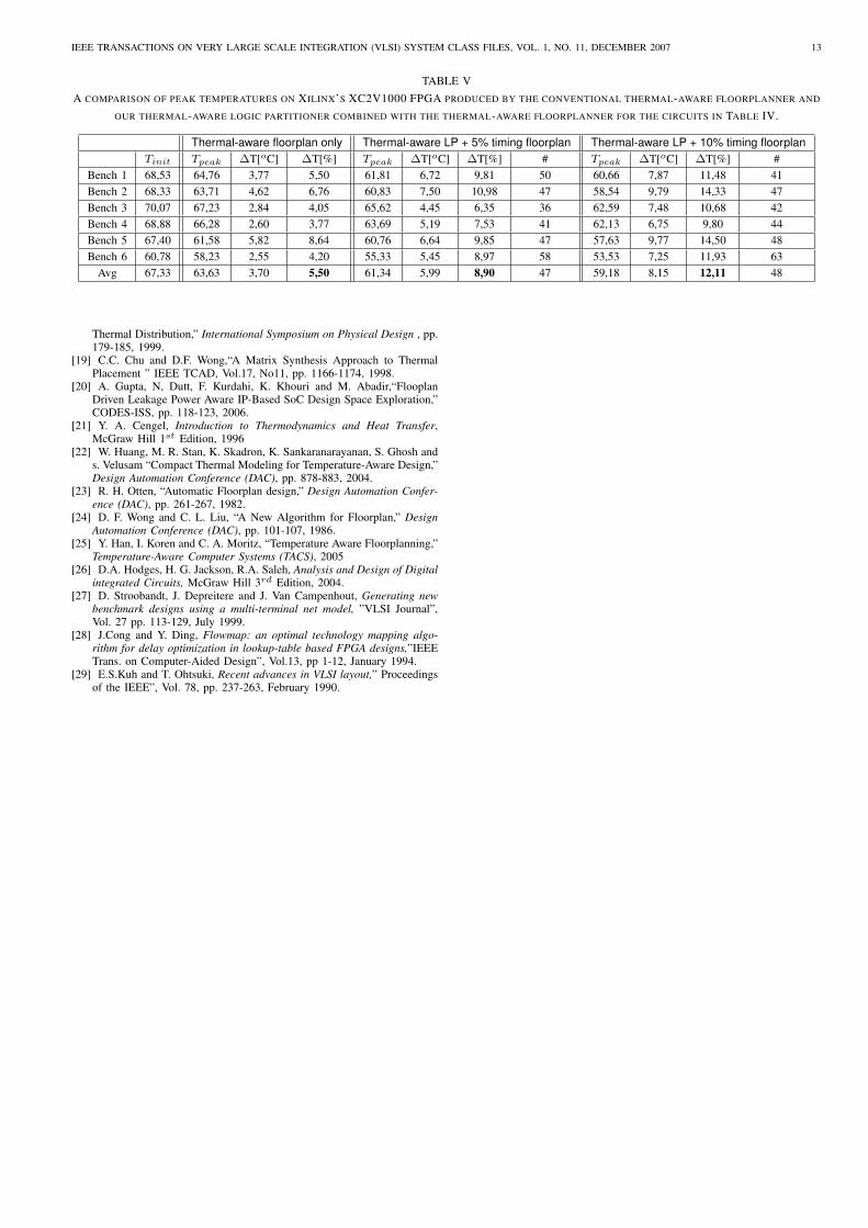
D. Experimental Results for FPGAs
Table V shows a comparison of peak temperatures usedby the three different approaches explained in the previoussection. It can be seen that for benchmarks Bench 1,2,5 and
TABLE IVTYPES AND SIZES OF FPGA BENCHMARK CIRCUITS
Benchmark Netlists (LUTs) # Total LUTsBench 1 syn 500, syn 1000, syn 1500, syn 2000 5000Bench 2 syn 500, syn 1500, syn 2000 , syn 2500 6500Bench 3 syn 500 , syn 1500 , syn 2000 , syn 3000 7000Bench 4 syn 1000 , syn 1500, syn 2500, syn 3000 8000Bench 5 syn 1000 , syn 2000, syn 2500, syn 3000 8500Bench 6 syn 1500, syn 2000, syn 2500, syn 3000 9000
6 our proposed technique LP-temp performs as expectedreducing the peak temperature in 8.90-10.98% for the tighttiming variant and 11.48-14.50% in the loose timing case. Inbenchmarks Bench 3 and 4 our proposed technique does notperform as well reducing the peak temperature less then therest of the benchmarks in each case due to the fact that ahotspot is located on a hardmacro (i.e. embedded multipliers).Our technique does only apply for logic netlists that canbe partitioned and re-placed. In the case where hardmacrosare hotspots our technique can reduce the temperature bypartitioning the hotspots close to the hardmacros with hotspotsand placing these as far away as possible as well as separatingthe hardmacros as far away as possible and surround them aswell as much as possible with cooler units. This explains whythe peak temperature is only reduced in the case of hardmacrosbeing hotspots by 6.35-7.53% in the tight timing constraintcase and 9.80-10.68% in the loose timing case.
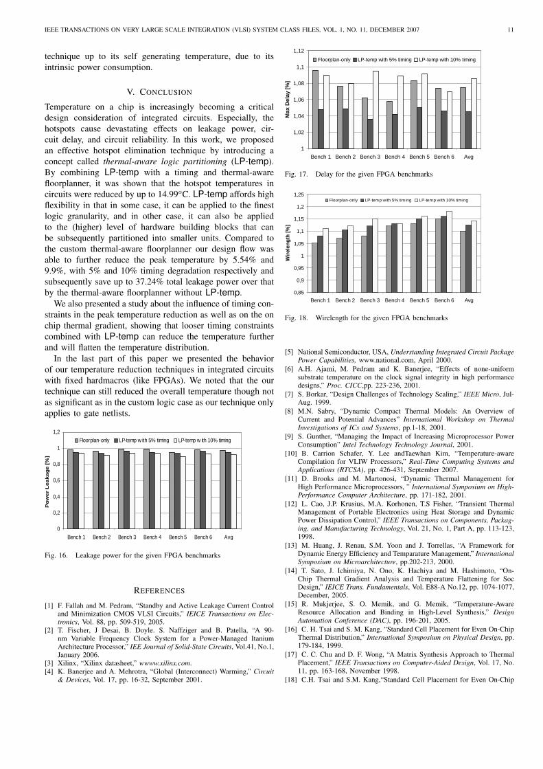
Figs. 16, 17, 18 show how different metrics (leakage power,maximum delay and total wirelength) change for each bench-mark. Leakage power is reduced between 5.11% using thethermal-aware floorplanner to 7.32% using the loose timingLP-temp.
Fig. 19 shows the thermal map of the FPGA in 5 differentscenarios for benchmark Bench 3. Fig. 19(a)shows the initialtemperature map before any temperature reduction techniqueis applied. 4 hotspots can be clearly identified. 2 in the FPGAslogic and 2 hotspots on the hardmacros. Fig. 19(b) showsthe thermal map after the thermal-aware floorplanner is ran.It can be noticed how Unit 3 has been rotated so that bothhotspots are not placed too close lowering the overall peaktemperature. Fig. 19(c) presents the thermal map after LP-temp is applied using a tight timing constraint (5%). Sameas in the logic gatenetlis case in Fig. 15(c) the hotspotscorresponding to the logic gatenetlist are weakened due tothe partitioning but can not be re-placed too far away dueto the tight timing constraints. As temperature is additivein nature the hardmacros’ peak temperature is therefore alsoreduced slightly. Fig.15(d) shows the thermal map of theFPGA after LP-temp is applied using a loose timing constraint(10%). Temperature in the logic gatenetlists hotspots is futherreduced as well as the temperature in the hardmacros as thehotter units are re-placed further away from them. The lastfigure (Fig.15(e))shows the final thermal map when not timingconstraints are used. the temperature is very even among mostof the FPGA except of the 2 hardmacros with the hotspotswhere the temperature can only be reduced applying our
IEEE TRANSACTIONS ON VERY LARGE SCALE INTEGRATION (VLSI) SYSTEM CLASS FILES, VOL. 1, NO. 11, DECEMBER 2007 11
technique up to its self generating temperature, due to itsintrinsic power consumption.
V. CONCLUSION
Temperature on a chip is increasingly becoming a criticaldesign consideration of integrated circuits. Especially, thehotspots cause devastating effects on leakage power, cir-cuit delay, and circuit reliability. In this work, we proposedan effective hotspot elimination technique by introducing aconcept called thermal-aware logic partitioning (LP-temp).By combining LP-temp with a timing and thermal-awarefloorplanner, it was shown that the hotspot temperatures incircuits were reduced by up to 14.99oC. LP-temp affords highflexibility in that in some case, it can be applied to the finestlogic granularity, and in other case, it can also be appliedto the (higher) level of hardware building blocks that canbe subsequently partitioned into smaller units. Compared tothe custom thermal-aware floorplanner our design flow wasable to further reduce the peak temperature by 5.54% and9.9%, with 5% and 10% timing degradation respectively andsubsequently save up to 37.24% total leakage power over thatby the thermal-aware floorplanner without LP-temp.
We also presented a study about the influence of timing con-straints in the peak temperature reduction as well as on the onchip thermal gradient, showing that looser timing constraintscombined with LP-temp can reduce the temperature furtherand will flatten the temperature distribution.
In the last part of this paper we presented the behaviorof our temperature reduction techniques in integrated circuitswith fixed hardmacros (like FPGAs). We noted that the ourtechnique can still reduced the overall temperature though notas significant as in the custom logic case as our technique onlyapplies to gate netlists.
0
0,2
0,4
0,6
0,8
1
1,2
Bench 1 Bench 2 Bench 3 Bench 4 Bench 5 Bench 6 Avg
Po
we
r L
ea
ka
ge
[%
]
Floorplan-only LP-temp w ith 5% timing LP-temp w ith 10% timing
Fig. 16. Leakage power for the given FPGA benchmarks
REFERENCES
[1] F. Fallah and M. Pedram, “Standby and Active Leakage Current Controland Minimization CMOS VLSI Circuits,” IEICE Transactions on Elec-tronics, Vol. 88, pp. 509-519, 2005.
[2] T. Fischer, J Desai, B. Doyle. S. Naffziger and B. Patella, “A 90-nm Variable Frequency Clock System for a Power-Managed ItaniumArchitecture Processor,” IEE Journal of Solid-State Circuits, Vol.41, No.1,January 2006.
[3] Xilinx, “Xilinx datasheet,” wwww.xilinx.com.[4] K. Banerjee and A. Mehrotra, “Global (Interconnect) Warming,” Circuit
& Devices, Vol. 17, pp. 16-32, September 2001.
1
1,02
1,04
1,06
1,08
1,1
1,12
Bench 1 Bench 2 Bench 3 Bench 4 Bench 5 Bench 6 Avg
Max
Del
ay [
%]
Floorplan-only LP-temp with 5% timing LP-temp with 10% timing
Fig. 17. Delay for the given FPGA benchmarks
0,85
0,9
0,95
1
1,05
1,1
1,15
1,2
1,25
Bench 1 Bench 2 Bench 3 Bench 4 Bench 5 Bench 6 Avg
Wir
elen
gth
[%]
Floorplan-only LP-temp with 5% timing LP-temp with 10% timing
Fig. 18. Wirelength for the given FPGA benchmarks
[5] National Semiconductor, USA, Understanding Integrated Circuit PackagePower Capabilities, www.national.com, April 2000.
[6] A.H. Ajami, M. Pedram and K. Banerjee, “Effects of none-uniformsubstrate temperature on the clock signal integrity in high performancedesigns,” Proc. CICC,pp. 223-236, 2001.
[7] S. Borkar, “Design Challenges of Technology Scaling,” IEEE Micro, Jul-Aug. 1999.
[8] M.N. Sabry, “Dynamic Compact Thermal Models: An Overview ofCurrent and Potential Advances” International Workshop on ThermalInvestigations of ICs and Systems, pp.1-18, 2001.
[9] S. Gunther, “Managing the Impact of Increasing Microprocessor PowerConsumption” Intel Technology Technology Journal, 2001.
[10] B. Carrion Schafer, Y. Lee andTaewhan Kim, “Temperature-awareCompilation for VLIW Processors,” Real-Time Computing Systems andApplications (RTCSA), pp. 426-431, September 2007.
[11] D. Brooks and M. Martonosi, “Dynamic Thermal Management forHigh Performance Microprocessors, ” International Symposium on High-Performance Computer Architecture, pp. 171-182, 2001.
[12] L. Cao, J.P. Krusius, M.A. Korhonen, T.S Fisher, “Transient ThermalManagement of Portable Electronics using Heat Storage and DynamicPower Dissipation Control,” IEEE Transactions on Components, Packag-ing, and Manufacturing Technology, Vol. 21, No. 1, Part A, pp. 113-123,1998.
[13] M. Huang, J. Renau, S.M. Yoon and J. Torrellas, “A Framework forDynamic Energy Efficiency and Temparature Management,” InternationalSymposium on Microarchitecture, pp.202-213, 2000.
[14] T. Sato, J. Ichimiya, N. Ono, K. Hachiya and M. Hashimoto, “On-Chip Thermal Gradient Analysis and Temperature Flattening for SocDesign,” IEICE Trans. Fundamentals, Vol. E88-A No.12, pp. 1074-1077,December, 2005.
[15] R. Mukjerjee, S. O. Memik, and G. Memik, “Temperature-AwareResource Allocation and Binding in High-Level Synthesis,” DesignAutomation Conference (DAC), pp. 196-201, 2005.
[16] C. H. Tsai and S. M. Kang, “Standard Cell Placement for Even On-ChipThermal Distribution,” International Symposium on Physical Design, pp.179-184, 1999.
[17] C. C. Chu and D. F. Wong, “A Matrix Synthesis Approach to ThermalPlacement,” IEEE Transactions on Computer-Aided Design, Vol. 17, No.11, pp. 163-168, November 1998.
[18] C.H. Tsai and S.M. Kang,“Standard Cell Placement for Even On-Chip

IEEE TRANSACTIONS ON VERY LARGE SCALE INTEGRATION (VLSI) SYSTEM CLASS FILES, VOL. 1, NO. 11, DECEMBER 2007 12
1 3 5 7 9 11 13 15S1
S5
S9
S13
0
10
20
30
40
50
60
70
80
Temperature [C]
70-8060-7050-6040-50
Unit1Unit2
Unit3
Mult1
Mult2
1 3 5 7 9 11 13 15S1
S5
S9
S13
0
10
20
30
40
50
60
70
80
Temperature [C]
70-80
60-70
50-60
40-50
Unit1 Unit2
Unit3
Mult1
Mult2
(a) Initial on-chip thermal distribution in the FPGA (b) Thermal distribution after thermal-aware floorplanner is executed in the FPGA
1 2 3 4 5 6 7 8 9 10 11 12 13 14 15S1
S5
S9
S13
0
10
20
30
40
50
60
70
80
Temperature [C]
70-80
60-70
50-60
40-50
Unit
Unit2_0
Unit3_0
Mult
Mult2
Unit2_1Unit2_2
Unit3_1
1 3 5 7 9 11 13 15S1
S5
S9
S13
0
10
20
30
40
50
60
70
80
Temperature [C]
70-80
60-70
50-60
40-50
Unit
Unit2_0
Unit3_0
Mult
Mult2
Unit2_1Unit2_2
Unit3_1
Unit2_3
Unit3_2 Unit3_3
(c) Thermal distribution after LP-temp with 5% timing constraint is executed in the FPGA (d) Thermal distribution after LP-temp with 10% timing constraint is executed in the FPGA
1 3 5 7 9 11 13 15S1
S5
S9
S13
0
10
20
30
40
50
60
70
Temperature [C]
60-70
50-60
40-50
UnitMult
Mult2
Unit2_0
Unit2_1
Unit2_2
Unit2_3
Unit3_0
Unit3_1
Unit3_2
(e) Thermal distribution after LP-temp with no timing constraint is executed in the FPGA
Fig. 19. On-chip thermal distributions for the techniques for benchmark 3 (Bench 3).
IEEE TRANSACTIONS ON VERY LARGE SCALE INTEGRATION (VLSI) SYSTEM CLASS FILES, VOL. 1, NO. 11, DECEMBER 2007 13
TABLE VA COMPARISON OF PEAK TEMPERATURES ON XILINX’S XC2V1000 FPGA PRODUCED BY THE CONVENTIONAL THERMAL-AWARE FLOORPLANNER AND
OUR THERMAL-AWARE LOGIC PARTITIONER COMBINED WITH THE THERMAL-AWARE FLOORPLANNER FOR THE CIRCUITS IN TABLE IV.
Thermal-aware floorplan only Thermal-aware LP + 5% timing floorplan Thermal-aware LP + 10% timing floorplanTinit Tpeak ∆T[oC] ∆T[%] Tpeak ∆T[oC] ∆T[%] # Tpeak ∆T[oC] ∆T[%] #
Bench 1 68,53 64,76 3,77 5,50 61,81 6,72 9,81 50 60,66 7,87 11,48 41Bench 2 68,33 63,71 4,62 6,76 60,83 7,50 10,98 47 58,54 9,79 14,33 47Bench 3 70,07 67,23 2,84 4,05 65,62 4,45 6,35 36 62,59 7,48 10,68 42Bench 4 68,88 66,28 2,60 3,77 63,69 5,19 7,53 41 62,13 6,75 9,80 44Bench 5 67,40 61,58 5,82 8,64 60,76 6,64 9,85 47 57,63 9,77 14,50 48Bench 6 60,78 58,23 2,55 4,20 55,33 5,45 8,97 58 53,53 7,25 11,93 63
Avg 67,33 63,63 3,70 5,50 61,34 5,99 8,90 47 59,18 8,15 12,11 48
Thermal Distribution,” International Symposium on Physical Design , pp.179-185, 1999.
[19] C.C. Chu and D.F. Wong,“A Matrix Synthesis Approach to ThermalPlacement ” IEEE TCAD, Vol.17, No11, pp. 1166-1174, 1998.
[20] A. Gupta, N, Dutt, F. Kurdahi, K. Khouri and M. Abadir,“FlooplanDriven Leakage Power Aware IP-Based SoC Design Space Exploration,”CODES-ISS, pp. 118-123, 2006.
[21] Y. A. Cengel, Introduction to Thermodynamics and Heat Transfer,McGraw Hill 1st Edition, 1996
[22] W. Huang, M. R. Stan, K. Skadron, K. Sankaranarayanan, S. Ghosh ands. Velusam “Compact Thermal Modeling for Temperature-Aware Design,”Design Automation Conference (DAC), pp. 878-883, 2004.
[23] R. H. Otten, “Automatic Floorplan design,” Design Automation Confer-ence (DAC), pp. 261-267, 1982.
[24] D. F. Wong and C. L. Liu, “A New Algorithm for Floorplan,” DesignAutomation Conference (DAC), pp. 101-107, 1986.
[25] Y. Han, I. Koren and C. A. Moritz, “Temperature Aware Floorplanning,”Temperature-Aware Computer Systems (TACS), 2005
[26] D.A. Hodges, H. G. Jackson, R.A. Saleh, Analysis and Design of Digitalintegrated Circuits, McGraw Hill 3rd Edition, 2004.
[27] D. Stroobandt, J. Depreitere and J. Van Campenhout, Generating newbenchmark designs using a multi-terminal net model, ”VLSI Journal”,Vol. 27 pp. 113-129, July 1999.
[28] J.Cong and Y. Ding, Flowmap: an optimal technology mapping algo-rithm for delay optimization in lookup-table based FPGA designs,”IEEETrans. on Computer-Aided Design”, Vol.13, pp 1-12, January 1994.
[29] E.S.Kuh and T. Ohtsuki, Recent advances in VLSI layout,” Proceedingsof the IEEE”, Vol. 78, pp. 237-263, February 1990.