IEEE TRANSACTIONS ON POWER ELECTRONICS 1 An Overview of Photonic Power Electronic...
13
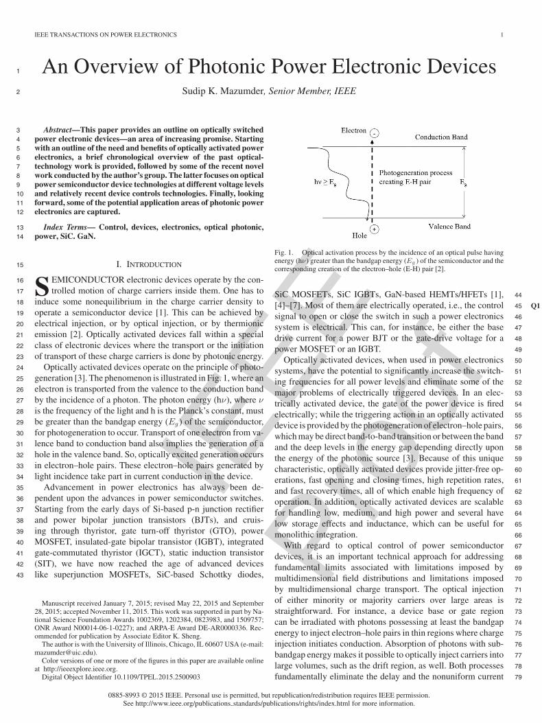
IEEE Proof IEEE TRANSACTIONS ON POWER ELECTRONICS 1 An Overview of Photonic Power Electronic Devices 1 Sudip K. Mazumder, Senior Member, IEEE 2 Abstract—This paper provides an outline on optically switched 3 power electronic devices—an area of increasing promise. Starting 4 with an outline of the need and benefits of optically activated power 5 electronics, a brief chronological overview of the past optical- 6 technology work is provided, followed by some of the recent novel 7 work conducted by the author’s group. The latter focuses on optical 8 power semiconductor device technologies at different voltage levels 9 and relatively recent device controls technologies. Finally, looking 10 forward, some of the potential application areas of photonic power 11 electronics are captured. 12 Index Terms— Control, devices, electronics, optical photonic, 13 power, SiC. GaN. 14 I. INTRODUCTION 15 S EMICONDUCTOR electronic devices operate by the con- 16 trolled motion of charge carriers inside them. One has to 17 induce some nonequilibrium in the charge carrier density to 18 operate a semiconductor device [1]. This can be achieved by 19 electrical injection, or by optical injection, or by thermionic 20 emission [2]. Optically activated devices fall within a special 21 class of electronic devices where the transport or the initiation 22 of transport of these charge carriers is done by photonic energy. 23 Optically activated devices operate on the principle of photo- 24 generation [3]. The phenomenon is illustrated in Fig. 1, where an 25 electron is transported from the valence to the conduction band 26 by the incidence of a photon. The photon energy (hν ), where ν 27 is the frequency of the light and h is the Planck’s constant, must 28 be greater than the bandgap energy (E g ) of the semiconductor, 29 for photogeneration to occur. Transport of one electron from va- 30 lence band to conduction band also implies the generation of a 31 hole in the valence band. So, optically excited generation occurs 32 in electron–hole pairs. These electron–hole pairs generated by 33 light incidence take part in current conduction in the device. 34 Advancement in power electronics has always been de- 35 pendent upon the advances in power semiconductor switches. 36 Starting from the early days of Si-based p-n junction rectifier 37 and power bipolar junction transistors (BJTs), and cruis- 38 ing through thyristor, gate turn-off thyristor (GTO), power 39 MOSFET, insulated-gate bipolar transistor (IGBT), integrated 40 gate-commutated thyristor (IGCT), static induction transistor 41 (SIT), we have now reached the age of advanced devices 42 like superjunction MOSFETs, SiC-based Schottky diodes, 43 Manuscript received January 7, 2015; revised May 22, 2015 and September 28, 2015; accepted November 11, 2015. This work was supported in part by Na- tional Science Foundation Awards 1002369, 1202384, 0823983, and 1509757; ONR Award N00014-06-1-0227); and ARPA-E Award DE-AR0000336. Rec- ommended for publication by Associate Editor K. Sheng. The author is with the University of Illinois, Chicago, IL 60607 USA (e-mail: [email protected]). Color versions of one or more of the figures in this paper are available online at http://ieeexplore.ieee.org. Digital Object Identifier 10.1109/TPEL.2015.2500903 Fig. 1. Optical activation process by the incidence of an optical pulse having energy (hν ) greater than the bandgap energy (E g ) of the semiconductor and the corresponding creation of the electron–hole (E-H) pair [2]. SiC MOSFETs, SiC IGBTs, GaN-based HEMTs/HFETs [1], 44 [4]–[7]. Most of them are electrically operated, i.e., the control Q1 45 signal to open or close the switch in such a power electronics 46 system is electrical. This can, for instance, be either the base 47 drive current for a power BJT or the gate-drive voltage for a 48 power MOSFET or an IGBT. 49 Optically activated devices, when used in power electronics 50 systems, have the potential to significantly increase the switch- 51 ing frequencies for all power levels and eliminate some of the 52 major problems of electrically triggered devices. In an elec- 53 trically activated device, the gate of the power device is fired 54 electrically; while the triggering action in an optically activated 55 device is provided by the photogeneration of electron–hole pairs, 56 which may be direct band-to-band transition or between the band 57 and the deep levels in the energy gap depending directly upon 58 the energy of the photonic source [3]. Because of this unique 59 characteristic, optically activated devices provide jitter-free op- 60 erations, fast opening and closing times, high repetition rates, 61 and fast recovery times, all of which enable high frequency of 62 operation. In addition, optically activated devices are scalable 63 for handling low, medium, and high power and several have 64 low storage effects and inductance, which can be useful for 65 monolithic integration. 66 With regard to optical control of power semiconductor 67 devices, it is an important technical approach for addressing 68 fundamental limits associated with limitations imposed by 69 multidimensional field distributions and limitations imposed 70 by multidimensional charge transport. The optical injection 71 of either minority or majority carriers over large areas is 72 straightforward. For instance, a device base or gate region 73 can be irradiated with photons possessing at least the bandgap 74 energy to inject electron–hole pairs in thin regions where charge 75 injection initiates conduction. Absorption of photons with sub- 76 bandgap energy makes it possible to optically inject carriers into 77 large volumes, such as the drift region, as well. Both processes 78 fundamentally eliminate the delay and the nonuniform current 79 0885-8993 © 2015 IEEE. Personal use is permitted, but republication/redistribution requires IEEE permission. See http://www.ieee.org/publications standards/publications/rights/index.html for more information.
Transcript of IEEE TRANSACTIONS ON POWER ELECTRONICS 1 An Overview of Photonic Power Electronic...
IEEE
Proo
f
IEEE TRANSACTIONS ON POWER ELECTRONICS 1
An Overview of Photonic Power Electronic Devices1
Sudip K. Mazumder, Senior Member, IEEE2
Abstract—This paper provides an outline on optically switched3power electronic devices—an area of increasing promise. Starting4with an outline of the need and benefits of optically activated power5electronics, a brief chronological overview of the past optical-6technology work is provided, followed by some of the recent novel7work conducted by the author’s group. The latter focuses on optical8power semiconductor device technologies at different voltage levels9and relatively recent device controls technologies. Finally, looking10forward, some of the potential application areas of photonic power11electronics are captured.12
Index Terms— Control, devices, electronics, optical photonic,13power, SiC. GaN.14
I. INTRODUCTION15
S EMICONDUCTOR electronic devices operate by the con-16
trolled motion of charge carriers inside them. One has to17
induce some nonequilibrium in the charge carrier density to18
operate a semiconductor device [1]. This can be achieved by19
electrical injection, or by optical injection, or by thermionic20
emission [2]. Optically activated devices fall within a special21
class of electronic devices where the transport or the initiation22
of transport of these charge carriers is done by photonic energy.23
Optically activated devices operate on the principle of photo-24
generation [3]. The phenomenon is illustrated in Fig. 1, where an25
electron is transported from the valence to the conduction band26
by the incidence of a photon. The photon energy (hν), where ν27
is the frequency of the light and h is the Planck’s constant, must28
be greater than the bandgap energy (Eg ) of the semiconductor,29
for photogeneration to occur. Transport of one electron from va-30
lence band to conduction band also implies the generation of a31
hole in the valence band. So, optically excited generation occurs32
in electron–hole pairs. These electron–hole pairs generated by33
light incidence take part in current conduction in the device.34
Advancement in power electronics has always been de-35
pendent upon the advances in power semiconductor switches.36
Starting from the early days of Si-based p-n junction rectifier37
and power bipolar junction transistors (BJTs), and cruis-38
ing through thyristor, gate turn-off thyristor (GTO), power39
MOSFET, insulated-gate bipolar transistor (IGBT), integrated40
gate-commutated thyristor (IGCT), static induction transistor41
(SIT), we have now reached the age of advanced devices42
like superjunction MOSFETs, SiC-based Schottky diodes,43
Manuscript received January 7, 2015; revised May 22, 2015 and September28, 2015; accepted November 11, 2015. This work was supported in part by Na-tional Science Foundation Awards 1002369, 1202384, 0823983, and 1509757;ONR Award N00014-06-1-0227); and ARPA-E Award DE-AR0000336. Rec-ommended for publication by Associate Editor K. Sheng.
The author is with the University of Illinois, Chicago, IL 60607 USA (e-mail:[email protected]).
Color versions of one or more of the figures in this paper are available onlineat http://ieeexplore.ieee.org.
Digital Object Identifier 10.1109/TPEL.2015.2500903
Fig. 1. Optical activation process by the incidence of an optical pulse havingenergy (hν) greater than the bandgap energy (Eg ) of the semiconductor and thecorresponding creation of the electron–hole (E-H) pair [2].
SiC MOSFETs, SiC IGBTs, GaN-based HEMTs/HFETs [1], 44
[4]–[7]. Most of them are electrically operated, i.e., the control Q145
signal to open or close the switch in such a power electronics 46
system is electrical. This can, for instance, be either the base 47
drive current for a power BJT or the gate-drive voltage for a 48
power MOSFET or an IGBT. 49
Optically activated devices, when used in power electronics 50
systems, have the potential to significantly increase the switch- 51
ing frequencies for all power levels and eliminate some of the 52
major problems of electrically triggered devices. In an elec- 53
trically activated device, the gate of the power device is fired 54
electrically; while the triggering action in an optically activated 55
device is provided by the photogeneration of electron–hole pairs, 56
which may be direct band-to-band transition or between the band 57
and the deep levels in the energy gap depending directly upon 58
the energy of the photonic source [3]. Because of this unique 59
characteristic, optically activated devices provide jitter-free op- 60
erations, fast opening and closing times, high repetition rates, 61
and fast recovery times, all of which enable high frequency of 62
operation. In addition, optically activated devices are scalable 63
for handling low, medium, and high power and several have 64
low storage effects and inductance, which can be useful for 65
monolithic integration. 66
With regard to optical control of power semiconductor 67
devices, it is an important technical approach for addressing 68
fundamental limits associated with limitations imposed by 69
multidimensional field distributions and limitations imposed 70
by multidimensional charge transport. The optical injection 71
of either minority or majority carriers over large areas is 72
straightforward. For instance, a device base or gate region 73
can be irradiated with photons possessing at least the bandgap 74
energy to inject electron–hole pairs in thin regions where charge 75
injection initiates conduction. Absorption of photons with sub- 76
bandgap energy makes it possible to optically inject carriers into 77
large volumes, such as the drift region, as well. Both processes 78
fundamentally eliminate the delay and the nonuniform current 79
0885-8993 © 2015 IEEE. Personal use is permitted, but republication/redistribution requires IEEE permission.See http://www.ieee.org/publications standards/publications/rights/index.html for more information.

IEEE
Proo
f
2 IEEE TRANSACTIONS ON POWER ELECTRONICS
Fig. 2. Illustration of a PCS [8].
density distributions associated with the electrical transport of80
charge carriers to the gate or base control regions of large power81
devices. However, there is another reason to consider optically82
activated power switches. The optical stimulation of deep trap83
levels can also remove mobile charge from the conduction and84
valence bands, thus providing a method for optically controlling85
a power semiconductor switch both ON and OFF.86
On a circuit level, the simple difference between optically87
and electrically activated systems results in some key additional88
advantages for the former. First, in an optically activated device,89
there is complete electrical isolation between the gate driver and90
the power stage. As such, very high di/dt and dv/dt, which may91
cause significant reliability problems in electrically activated92
devices at high switch frequencies, have limited impact on an93
optically activated devices. Therefore, the basic architecture of94
the gate driver in an optically activated device is simple. Sec-95
ond, for two- and higher level electrically triggered switching96
converters, different designs of low- and high-side drivers are re-97
quired; the latter is especially challenging to design for medium98
and high-power applications.99
For an optically activated converter, the designs of high- and100
low-side drivers remain the same. Third for firing optically acti-101
vated devices, optically multiplexed triggering signals (as often102
encountered in modern optical-fiber based control systems) do103
not need to be converted back to electrical signals. This leads104
to simplicity of overall design, enhanced controlled bandwidth,105
enhanced reliability of the system, and monolithic integration.106
Fourth, as the switching frequency of an electrically activated107
device increases, parasitic oscillations may be induced in the108
driver circuit owing to coupling effects between the device ca-109
pacitance and the parasitic inductance of the gate connection and110
also due to transmission-line effects. This may lead to failure111
of the gate driver; with an optically activated device such pos-112
sibilities do not arise. Clearly, optically activated devices have113
the potential to address these problems encountered in conven-114
tional electrically activated devices. They are emerging devices115
for power electronics applications and much research is ongoing116
as well as needed on in this area.117
While Section I provides the introduction to the photonic118
devices for power electronics, Section II provides an overview119
on the past work in this area. Sections III provides an outline on120
recent and ongoing work primarily at author’s group as outlined121
in the abstract. The distinction between the past and recent work122
is simply that while the former work has concluded, the latter123
continues to be the basis for some of the ongoing work. Section124
IV provides an overview of work that is going to be and/or125
Fig. 3. Schematic of a photodiode.
can be potentially realized further extending the promise of 126
applications of photonic devices for power electronics. Finally, 127
in Section V, a qualitative assessment of the broad category of 128
optically switched devices outlined in this manuscript has been 129
provided from the standpoint of their applicability for power 130
electronics. 131
II. PAST WORK 132
One of the main uses of optical activation and control could be 133
enabling a different scaling law for the design of high blocking- 134
voltage power devices. The depletion region charge distribu- 135
tion fundamentally limits the blocking voltage in conventional 136
devices. Even then the fundamental limit is seldom achieved 137
because surfaces and curvature in the doped regions produce 138
electric field magnitudes in excess of the critical value at re- 139
duced voltage. 140
A conceptually different approach uses a neutral semiconduc- 141
tor with very low equilibrium conductivity between two ohmic 142
contacts to block larger voltages. This approach, the heart of the 143
photoconductive switch (PCS) [8] and as illustrated in Fig. 2, 144
typically uses a semiinsulating (SI) semiconductor. There are 145
two operating modes of PCS that have been researched rather 146
extensively. The first is the optically activated PCS (with photo- 147
conductive gain greater than one) and the second is the optically 148
sustained PCS (with photoconductive gain less than one). 149
There are advantages and disadvantages of the optically ac- 150
tivated PCS in power electronics. One advantage is the voltage 151
scalability of the PCS by increasing the linear dimension. Thus, 152
a single PCS can be made to handle much larger voltages than a 153
typical conventional power switch (e.g., thyristor or IGBT). An- 154
other advantage is that the regenerative conduction mechanism 155
is not easily triggered by electrical means, making an optically 156
activated PCS virtually immune to spurious dv/dt triggering in 157
the conventional power electronics applications. Indeed, the di- 158
electric strength of the PCS usually increases under transient 159
voltages (i.e., with increasing dv/dt) [9]. The combination of 160
fewer switches and optical triggering can simplify the design of 161
a multivalve converter. 162
The main disadvantage with the conventional PCS design 163
is that it is difficult to design the switch for a useful blocking 164

IEEE
Proo
f
MAZUMDER: OVERVIEW OF PHOTONIC POWER ELECTRONIC DEVICES 3
Fig. 4. Si-based LTT [13].
Fig. 5. OT-MOS structure.
voltage and an acceptable conduction loss while achieving an ac-165
ceptable average power from the activating optical source. Con-166
sequently, there are no widely accepted, commercially available167
PCS for power electronics applications. For power electronics168
applications, the laser energy required to sustain conduction is169
prohibitive. These PCS devices appear limited to highly special-170
ized pulsed-power applications.171
There is another attractive physical mechanism available in172
optically activated power switches via optical stimulation of173
deep trap levels yielding a mechanism for optically controlling174
the conduction state of power semiconductor switches both ON175
and OFF. The observation of infrared quenching of photocon-176
ductivity in copper-doped GaAs was reported in [10]. Infrared177
quenching in copper-doped semiinsulating GaAs has been ap- 178
plied to the PCS concept to produce the bistable opticallystim- 179
ulated switch (BOSS) [11]. 180
The BOSS, fabricated as a conventional PCS, shares the ad- 181
vantages and disadvantages of the optically activated (closing) 182
PCS described previously without suffering, to the same degree, 183
the inefficiency of the optically sustained (naturally opening) 184
PCS. However, the need for sources with two separate laser 185
wavelengths increases complexity and cost, and the problem of 186
designing an efficient cost-effective PCS for power electronics 187
applications remains. One solution could be to include the op- 188
tically active material that forms BOSS in the control region of 189
a conventional power semiconductor switch, such as the base 190

IEEE
Proo
f
4 IEEE TRANSACTIONS ON POWER ELECTRONICS
(a)
(b)
(c)
Fig. 6. (a) Device structure of the lateral OTPT; (b) Micrograph of the OTPT;and (c) Packaged realization of the OTPT.
of an optically activated BJT or the channel of an optically191
activated MOSFET.192
One way to preclude the need for two light sources in BOSS193
without compromising the repetition rate while ensuring high194
gain (and hence, lower beam intensity) is using optically acti-195
vated lateral and vertical p-i-n diodes, a few of which have been196
reported in [12] and [13]. Most of these devices are targeted for197
low-frequency but high-power applications (e.g., pulsed-power198
switching or microwave power generation). Fig. 3 illustrates a199
simple p-i-n diode schematic with the incident optical beam and200
the photogeneration in the intrinsic region. Normally, the diode201
is reverse biased and conducts very small dark current in its202
off-state. When the light falls on it through an optical window,203
excess carriers are generated due to high electric field and the204
conductivity increases manyfold and the diode conducts cur-205
rent. However, high electric field in such devices often yields206
long-term reliability issues.207
A bipolar optical device that overcomes the limitation of208
reverse-bias optical diode while ensuring voltage stability even209
Fig. 7. (a) Three-dimensional view of the electric-field distribution inside theOTPT at the instant of breakdown. (b) Three-dimensional view of the uniformphotogeneration rate inside the OTPT.
at high voltages is the light-triggered thyristor (LTT) [14], [15]. 210
A typical light triggering of thyristor is achieved by localized 211
illumination at a centered site of the device. There is an optical 212
well and surrounding it there lay a pilot thyristor and an am- 213
plifying thyristor structure. Photogenerated electron–hole pairs 214
cause a lateral current flow from the center of the well, driven 215
by the anode bias. This lateral current induces a voltage drop 216
in the main cathode junction, which is sufficient to turn ON 217
the pilot thyristor. The pilot thyristor then turns ON the larger 218
amplifying thyristor. This, in turn, is able to drive the gate arms 219
of the main device. The well is very sensitive and normally few 220
microjoule of optical energy is sufficient for taking the device 221
into full conduction from a reverse blocking state. Sometimes, 222
there can be more than one amplifying gates depending upon the 223
current requirement of the device. Fig. 4 shows a schematic of 224
an LTT based on Si material base. An LTT could be an elegant 225
device for many applications, especially at high power. It can 226
yield high reliability and compact system design. Further, op- 227
tical activation leads to enhanced immunity to electromagnetic 228
noise and isolation between control and power stages. How- 229
ever, Si-based LTTs are not suitable for fast switching at high 230
voltage. 231
Unlike the LTT, conventional optothyristors are normally 232
made of III–V compounds such as GaAs, AlGaAs, and InP. 233
Direct-bandgap nature of these materials allows optical effi- 234
ciency and switching speed to be higher and also facilitates 235

IEEE
Proo
f
MAZUMDER: OVERVIEW OF PHOTONIC POWER ELECTRONIC DEVICES 5
(a)
(b)
Fig. 8. (a) Experimental OTPT on-resistance with varying optical power underthe following conditions: VBias = 10 V, Rload = 50 Ω, frequency = 5 kHz,and duty cycle = 50%. (b) X–Y phase plot of the OTPT voltage with opticalsignal illustrating the nonlinear variation of conductivity with optical powervariation.
heterostructures to be explored [16]. Although successful236
fabrication and application of optothyristors have been demon-237
strated for high-voltage pulsed-power systems [16], [17], sur-238
face degradation, edge breakdown, and deep-level effects of239
the semiinsulating base layer can lead to early breakdown at a240
voltage much less than the theoretical value. As such, careful241
design optimization is a necessity. Another interesting approach242
has been reported in [18] to integrate the optical-control detec-243
tion circuitry with power device and to create an LTT with an244
MOS amplifying gate structure.245
Unlike the bipolar devices, among the power semiconduc-246
tor devices, MOSFET is the most preferred choice for high-247
frequency applications due to its unipolar conduction, which248
does not introduce any minority carrier storage delay. How-249
ever, optical switching of power MOSFETs has not been stud-250
ied much. Optical control of the MOSFET or MIS structure, in251
general, has been reported in [19] and [20]. But, they are primar-252
ily in the domain low-power optical communication or sensor253
applications. Modulation techniques for an optically triggered254
power MOSFET (OT-MOS) has been reported in [21]. A ver-255
tical double-diffused MOS (DMOS) is controlled by a turn-on256
and a turn-off pulse and the hybrid device structure schematic,257
comprising a Si-based DMOS, a GaAs-based photodiode, and a258
GaAs-based PCS, is shown in Fig. 5. The photodiode acts as a259
photogenerated current source, which, upon shining the turn-on260
(a)
(b)
(c)
(d)
Fig. 9. Experimental switching dynamics of the OTPT under the followingconditions: VBias = 60 V, Rload = 1000 Ω, frequency = 50 kHz, and dutycycle = 50%.
pulse on it, modulates the i-drift region resistance, conducts cur- 261
rent (supplied by the reverse bias source) and charges the gate 262
capacitance of the DMOS above the threshold voltage to turn the 263
OT-MOS ON. Again, during turn-off, another optical pulse falls 264
on the PCS to modulate its conductivity, provides a short-circuit 265
path through the PCS, and discharge the gate capacitance of the 266
DMOS to turn it OFF. So, the turn-on and turn-off time can be 267

IEEE
Proo
f
6 IEEE TRANSACTIONS ON POWER ELECTRONICS
Fig. 10. OTPT-based switching of (a) Si-based power MOSFET, (b) Si-based IGBT, (c) SiC-based VJFET, and (d) SiC-based MOSFET. The dynamics of theSiC MOSFET is comparatively slower due to the high input capacitance of the device and is not attributed to the OTPT.
adjusted either by manipulating the amplitudes of the photo-268
generated current-source strength and PCS conductivity or by269
varying the time period of the triggering pulses, thus allowing270
the gate capacitance of the OT-MOS to charge or discharge for271
a varying time. Consequently, there are possibilities of using272
both amplitude- and pulsewidth modulation techniques for the273
activating optical pulses [22], [23].274
In line with above optically activated field-effect devices, an275
approach to activate an IGBT with a direct optical pulse, incident276
in its channel region has been reported in [24]. It shows improve-277
ment in the on-state voltage drop of the optically activated IGBT278
given that the channel width in this case depends upon the ab-279
sorption depth for the particular semiconductor material-optical280
wavelength pair and it can be significantly higher than the intrin-281
sic Debye length (a few nanometer), which is the default channel282
width for an MOSFET. However, Liao et al. [24] treated only the283
improved current density and voltage drop and does not report284
switching results for the optically activated IGBT. Yet another285
photonic field-effect device is the optically activated MESFET286
[25]. When the device is illuminated with light, with photon287
energy greater than the bandgap energy, illuminated channel288
region contributes optically activated gate photocurrent. Illumi-289
nated interelectrode epilayer photocurrent modulates the con-290
ductivity of the epilayer. Also in the episubstrate barrier region291
excess photogenerated carriers reduce the barrier height and292
the illuminated part of the substrate contributes to the substrate293
current. Finally, in [26], another field-effect device—optically294
modulated series-coupled SIT—is outlined. In it, the ground- 295
referenced low-power optical trigger sources are isolated from 296
the high-voltage switch assembly through optical fibers, and this 297
results in reliable, jitter-free operation [26]. Optically activated 298
SITs are also made from III–V materials to leverage the advan- 299
tage of high critical electric field and higher carrier mobility of 300
these elements. 301
III. RECENT AND ONGOING WORK 302
Fig. 6 shows the device structure of a GaAs-based optically 303
triggered power transistor (OTPT), micrograph of a prototype 304
OTPT, and its packaged realization [27]. GaAs has a high level of 305
light absorption, and hence, a high quantum efficiency. Further, 306
the rectangular electric field enabled by the RESURF structure 307
enables reduced effective distance between collector and emit- 308
ter electrodes of the OTPT and yields higher optical gain. Also, 309
a rectangular electric field [see Fig. 7(a)] mobilizes the pho- 310
togenerated carriers in a uniform manner, as demonstrated in 311
Fig. 7(b). The quantum efficiency and the switching speed of 312
the OTPT depend strongly on the minority-carrier recombina- 313
tion lifetime in the p-body region. The on-state resistance of the 314
OTPT varies with the optical intensity as shown in Fig. 8(a), 315
while Fig. 8(b) demonstrates the nonlinear variation of conduc- 316
tivity with optical power variation for the OTPT. Snapshots of 317
the turn-on and turn-off dynamics of the OTPT are shown in 318
Fig. 9. 319

IEEE
Proo
f
MAZUMDER: OVERVIEW OF PHOTONIC POWER ELECTRONIC DEVICES 7
Fig. 11. (a), (b) Switching waveforms at 400-V bias, 20 kHz, and at 200 °C case temperature with duty cycles of (a) 5% and (b) 90%. (c) and (d) Switchingwaveforms at 400-V bias, 10% duty cycle, and at 200 °C case temperature with frequencies of (c) 10 kHz and (d) 50 kHz.
Subsequent to the evaluation of the OTPT, the concept of op-320
tically activated hybrid power semiconductor device was tried321
using a combination of triggering OTPT(s) and high-voltage de-322
vices such as SiC MOSFET, SiC VJFET, Si IGBT, and Si MOS-323
FET devices. Fig. 10 [27] shows the transient performance of324
such optical hybrid devices. Such integrated hybrid device work325
has been carried further for high temperature operation. For in-326
stance, Fig. 11 shows the transient operation of an OTPT-based327
SiC MOSFET at 200 °C under varying pulse width and duty cy-328
cle for frequencies ranging from 10 to 50 kHz. This demonstrates329
the photonic control of SiC MOSFET at high temperature over330
a range of switching conditions. It is worthwhile noting here331
that if very-high-speed switching dynamics is not a necessity,332
then a higher gain multistage OTPT can be used to significantly333
reduce the optical power requirement while accepting a slightly334
slower switching speed. Fig. 12 illustrates this point using an335
MOSFET being driven by a two-stage OTPT driver.336
More recently, a vertical OTPT based on Si has been designed,337
fabricated, and characterized that can support much higher cur-338
rent of operation and fast switching dynamics [28]. The device339
is designed to support a junction temperature of 200 °C. Even340
though the initial goal of the OTPT is to support an optically341
triggered emitter turn-off thyristor, the vertical OTPT can be342
used independently and for other hybrid configurations. Figs.343
13 and 14 demonstrate the information regarding the OTPT.344
An applicability of the OTPT has been captured via a re- 345
cent patent [29] that outlines a single-biased all-optical emitter- 346
turn-off (ETO) thyristor. Fig. 15(a) outlines the structure of the 347
device. The initial results based on different embodiments of 348
OTPTs have been reported in [28], [30], and [31] and are en- 349
couraging. One such result at high current is shown in Fig. 15(b). 350
There are basic solutions to mitigate the undesired turn-on of 351
the gate (which is an issue for the conventional self-gated elec- 352
trically activated ETO as well) including 1) reducing packag- 353
ing parasitic inductance, 2) choosing n-MOSFET with higher 354
threshold voltage, 3) a standard solution of placing a Zener diode 355
in the gate-to-drain path of the n-MOSFET, and 4) adding an- 356
other p-MOSFET in series with the n-MOSFET. Solution 4 mit- 357
igates the gate current during turn-on but leads to an additional 358
p-MOSFET die of the same current rating as the n-MOSFET. 359
The solution c leads to an additional Zener diode but its current 360
rating is less compared to the p-MOSFET since it is placed in 361
the path of the gate of the n-MOSFET. Solution 2 is coupled 362
to the di/dt, thyristor forward drop, and packaging inductance. 363
Notwithstanding the approaches outlined in b through d, reduced 364
packaging inductance has an overall benefit, especially at very 365
high di/dt. If successfully realized, the all-optical single-bias 366
ETO structure in Fig. 15(a), has key advantages over electri- 367
cally activated ETO [32], MTO, and IGCT. Work is ongoing in 368
this regard. 369

IEEE
Proo
f
8 IEEE TRANSACTIONS ON POWER ELECTRONICS
(a)
(b) (c)
(d) (e)
Fig. 12. (a) Two-stage higher gain OTPT-based driver triggering a Si MOSFET. (b) and (c) Rise and fall times of (a) with 50-mW optical power. (d) and (e)Corresponding rise and fall times of a single-stage OTPT-based driver triggering Si MOSFET.
Apart from synthesis of optically activated power semicon-370
ductor devices that meet emerging performance needs, there is371
a need to control the light-delivery mechanism to switch the372
optical device appropriately. Initial work in this regard using373
OTPT-based control has been outlined in [33], which outlines374
the need for switching-transition control outlined in [34]. For375
instance, Fig. 16 shows how the increment in the OTPT optical376
intensity leads to reduction in the Miller-plateau width of a Si377
CoolMOS. Subsequent work has advanced these initial works378
with additional technological capabilities as captured in [35]379
and [36]. Fig. 17 demonstrates one such experimental controller 380
for the optical device developed recently [36]. 381
IV. FUTURE WORK AND POTENTIAL OPPORTUNITIES 382
Looking at the historical work and observing the areas of 383
applications where electrical activation of power semiconduc- 384
tor devices have had reliability issues, there are several areas 385
of applications where optically activated power electronics and 386
switched-power-system technology is applicable and beneficial. 387

IEEE
Proo
f
MAZUMDER: OVERVIEW OF PHOTONIC POWER ELECTRONIC DEVICES 9
Fig. 13. Vertical experimental OTPT device geometry, packaging architecture,and actual package.
One core commonality in some of these applications appears to388
be the high dv/dt and di/dt, which transcends very high volt-389
age and moderate frequency as well as low voltage and very390
high frequency (VHF). For instance, for next-generation optical391
semiconductor-device-based high-voltage solid-state electronic392
control and power-quality applications at transmission and dis-393
tribution levels, photonic power electronics technology (e.g.,394
[29], [37], [38], and others) provides advantages with regard to395
enhanced reliability, seamless scalability, efficient operability,396
and dynamic controllability. Needless to say, some of the advan-Q2
397
tages carry over to other legacy as well as emerging applications398
(e.g., transfer and grid-isolation switches of a microgrid, high-399
voltage and high-power motor drive and power-quality-related400
conditioners, medium-voltage electric-traction locomotive) but401
need to be evaluated on a case by case basis.402
Yet another set of high-power application encompasses403
pulsed-power systems [39]–[41] and rapid fault isolation. These404
applications, unlike typical power electronic applications, typ-405
ically require rapid burst of energy in a short duration of time406
with minimal switching-initiation delay under conditions of rel-407
atively slow repeatability. Fig. 18 illustrates a GaN-based optical408
pulsed-power switch [42] that is rapidly activated optically with409
a rise time of about 10 ns. The activation is achieved at high410
gain using a monolithically integrated MISFET that provides a411
transient high electric field just before the device is activated.412
During the near-singularity event that leads to high di/dt, opti-413
cal technology provides enhanced immunity to electromagnetic414
Fig. 14. Experimental I–V and switching characterizations of the verticalOTPT outlined in Fig. 13.
noise (as illustrated in Fig. 19 [43]) and the direct- 415
photogeneration capability reduces switching-onset delay. Sev- 416
eral of the advantages of high-voltage and high-current photonic 417
power electronics and switched-power-systems technologies re- 418
main even at lower voltages with progressively enhanced tan- 419
gible benefits at VHF and ultrahigh frequency of operation. 420
Areas of such applications can be power amplifiers for wire- 421
less communication and power amplifiers for radars. Another 422
set of application encompasses system technologies such as 423
fly-by-light for aerospace and avionics [43] or electric-vehicle 424
applications with coexistence of electrical-power and electronic- 425
communication systems. Yet another application encompasses 426
dealing with electrical and electronic systems with plurality of 427
floating grounds. Finally, and on a more recent note, the ability 428
of power electronic system to support normal as well as fault 429
modes of operation is being sought. A key to that resides with 430
the power semiconductor device. Fig. 20 shows an early con- 431
ceptual result in that regard. It illustrates how an OTPT-based 432
optically controlled SiC MOSFET’s on-state drop can be rela- 433
tively easily controlled simply by adjusting the optical intensity 434
of the OTPT. Thus, under normal operation, the optical inten- 435
sity is so controlled such that the MOSFET drop is nominal 436
(which is small), but at the onset of the fault, the intensity can 437
be so controlled such that the MOSFET on-state drop is quickly 438
increased thereby limiting the current. 439

IEEE
Proo
f
10 IEEE TRANSACTIONS ON POWER ELECTRONICS
Fig. 15. (a) Structure of the single-bias all-optical ETO. LG and LA representthe packaged parasitic inductance. The high-voltage device is a SiC thyristor.(b)–(d) Initial results for the structure shown in (a) using a high-gain OTPT. (b)Voltage across the load and the optical control signal on the OTPT. (c) Outputcurrents for the thyristor in the optically triggered ETO. (d) ETO on-state voltageand leakage current as controlled by the OTPT p-base thickness variation.
Overall, these outlined potential areas are by no means all en-440
compassing. It is not unrealistic to surmise that additional areas441
of applications where photonic power electronics and switched-442
power-systems makes tangible impact are being pursued and/or443
being explored. Of course the viable realization of existing and444
emerging application will benefit significantly with continual445
Fig. 16. Modulation of the Miller plateau of a Si CoolMOS (driven by OTPT)with varying optical intensity of the OTPT activation.
Fig. 17. (a) Experimental optical controller: fabricated board, which includespower circuit, control circuit, laser, and laser driver. (b) and (c) Packaged deviceused that uses the GaAs-based OTPT shown in Fig. 6(a).

IEEE
Proo
f
MAZUMDER: OVERVIEW OF PHOTONIC POWER ELECTRONIC DEVICES 11
Fig. 18. (a) Lateral view of the GaN-based insulated-gate photoconductivesemiconductor switch (IGPCSS). (b) Equivalent circuit model of the IGPCSSdevice (middle), illustrating the schematic diagrams of a bias source (left) andthe timing sequence of trigger signals (right). (c) Bottom view of the GaN-based IGPCSS. The multicell-parallel insulted gates are arrayed with the shapeof hexagonal honeycomb.
advancements in device realization and control implementation446
technologies. With regard to the former, new innovations in wide447
bandgap as well as narrow-bandgap device structures, materials,448
light-delivery mechanisms, and optoelectronic thermal packag-449
ing would of help. With regard to optical control, mechanisms450
of multiscale, dynamic, and reconfigurable switching-sequence-451
based and switching-transition controls [34], [44], [45] that ex-452
ploit the unique and distinguishing properties of the optically453
activated and optically controlled devices needs to be explored454
and pursued.455
V. SUMMARY AND CONCLUSION456
In this paper, an overview has been provided on photoni-457
cally switched devices with potential applications for power458
(a)
(b)
Fig. 19. Illustration of the difference in mechanism between (a) electricallyactivated and (b) optically activated power electronics technologies indicatingthe advantages associated with immunity from electromagnetic interference(EMI), electrical isolation between power and control stages, and reduced devicetriggering delay.
electronics. Initially, an overview has been provided on the suit- 459
ability of optically switched device technologies for application 460
space encompassing device and circuit and systems levels. At 461
the device level, initially an outline on the past work encom- 462
passing PCS and BOSS devices, which yield rapid switching at 463
the cost of higher optical power, is provided. The mechanism 464
to increase optical gain using minority-carrier reverse-biased 465
diode is provided next that yield simple structure with high gain 466
at the cost of long-term reliability issue due to high electric 467
field. The latter is addressed using the LTT and optothyristor; 468
they yield support for high-voltage and periodic-switching ap- 469
plications but at the cost of latching that complicates turn-off 470
transition. Subsequently, an outline on devices that integrate op- 471
tical actuation to traditional majority-carrier field-effect struc- 472
tures (e.g., MOSFET, IGBT, MISFET, SIT) has been provided. 473
Since such devices require charge separation while the optical 474
beam comprises charge-neutral photons, indirect device struc- 475
tures are often required for switching or light can be used for 476

IEEE
Proo
f
12 IEEE TRANSACTIONS ON POWER ELECTRONICS
Fig. 20. Experimental demonstration of the OTPT-based photonic modula-tion of the gate voltage level of the SiC MOSFET and corresponding forwardconduction drop variation.
channel-impedance modulation. Based on realizations accrued477
from the past work, recent and ongoing work that address some478
of these issues are outlined. These improvements are classified479
in three categories. First, an all optical monolithic OTPT that480
leverages III–V direct bandgap material is explored, which ad-481
dress speed while limiting the need for higher optical power.482
Second, instead of a monolithic approach a separation of func-483
tionalities in a hybrid device using a triggering OTPT and a484
driving power semiconductor device is explored. This enables485
one to use different material base for the two stages, thereby,486
optimizing the characteristics and explore both bipolar as well487
as field-effect devices for the power stage, thereby, optimally488
addressing gain-speed tradeoff. The third approach is one of489
scaling the hybrid configuration for very high voltage using490
an optical SiC-based ETO structure. The latter overcomes the491
turn-off-speed limitation of the LTT and optothyritors using an492
intelligently placed OTPT, thereby, yielding much operating fre-493
quency even at high voltage. Finally, an outline on the emerging494
work has been provided that relies on these recent devices out-495
lined previously and some recent GaN-based PCS devices. The496
focus of this study is primarily on dynamic switching dynam-497
ics controllability of these photonically activated devices for498
yielding multiple system-level benefits for power electronics.499
ACKNOWLEDGMENT500
The author would like to thank his previous and current grad-501
uate students (Dr. T. Sarkar, Mr. A. Mojab, and Dr. H. Riazmon-502
tazer), Visiting Scholar (Prof. X. Wang), Dr. B. Passmore (Cree,503
Inc.), Dr. A. Agarwal (DOE), Dr. L. Cheng (ARL), Dr. D. Grider504
(Cree, Inc.), Dr. A. Sugg (Vegawave, Inc.), and also thanks the505
support of Dr. G. Maracas (DOE), Dr. P. Maki (ONR), Dr. Eyad506
Abed (NSF), Dr. K. Baheti (NSF), and Dr. T. Heidel (ARPA-E).507
Any opinions, findings, conclusions, or recommendations 508
expressed herein are those of the authors and do not necessarily 509
reflect the views of the NSF. 510
REFERENCES 511
[1] B. J. Baliga, Fundamentals of Power Semiconductor Devices. New York, 512NY, USA: Springer, 2008. 513
[2] S. K. Mazumder, T. Sarkar, M. Dutta, and M. Mazzola, “Photoconductive 514devices for power electronics,” Electrical Engineering Handbook, 3rd ed. 515New York, NY, USA: Taylor & Francis, 2005, pp. 943–958. 516
[3] P. Bhattacharya, Semiconductor Optoelectronic Devices. Englewood 517Cliffs, NJ, USA: Prentice Hall, 1994. 518
[4] J. Lutz, H. Schlangenotto, U. Scheuermann, and R. D. Docker, Semicon- 519ductor Power Devices. New York, NY, USA: Springer, 2011. 520
[5] B. J. Baliga, Silicon Carbide Power Devices. Singapore: World Scientific, 5212006. 522
[6] X. Huili, Y. Dora, A. Chini, S. Heikman, S. Keller, and U. K. Mishra, 523“High breakdown voltage AlGaN-GaN HEMTs achieved by multiple field 524plates,” IEEE Electron Device Lett., vol. 25, no. 4, pp. 161–163, Apr. 2004. 525
[7] N. Ikeda, S. Kaya, L. Jiang, Y. Sato, S. Kato, and S. Yoshida, “High power 526AlGaN/GaN HFET with a high breakdown voltage of over 1.8 kV on 4 527inch Si substrates and the suppression of current collapse,” in Proc. 20th 528Int. Symp. Power Semicond. Devices IC’s, 2008, pp. 287–290. 529
[8] A. Rosen and F. Zutavern, High Power Optically Activated Solid-State 530Switches, Norwood, MA, USA: Artech House, Jan. 1994. 531
[9] G. M. Loubriel, M. W. O’Malley, F. J. Zutavern, B. B. McKenzie, 532W.R. Conley, and H. P. Hjalmarson, “High current photoconductive semi- 533conductor switches,” in Proc. IEEE 18th Power Modulator Symp., 1988, 534pp. 312–317. 535
[10] J. Blanc, R. H. Bube, and H. E MacDonald, “Properties of high-resistivity 536gallium arsenide compensated with diffused copper,” J. Appl. Phys., 537vol. 32, pp. 1666–1679, 1961. 538
[11] M. S. Mazzola, K. H. Schoenbach, V. K. Lakdawala, and S. T. Ko, 539“Nanosecond optical quenching of photoconductivity in a bulk GaAs 540switch,” Appl. Phys. Lett., vol. 55, pp. 2102–2104, 1989. 541
[12] A. Rosen, P. Stabile, W. Janton, A. Gombar, P. Basile, J. Delmaster, and 542R. Hurwitz, “Laser-activated p-i-n diode switch for RF application,” IEEE 543Trans. Microw. Theory Tech., vol. 37, no. 8, pp. 1255–1257, Aug. 1989. 544
[13] A. Rosen, P. Stabile, A. M. Gombar, W. M. Janton, A. Bahasadri, and 545P. Herczfeld, “100 kW dc biased, all semiconductor switch using Si 546pin diodes and AlGaAs 2-D laser arrays,” IEEE Photon. Technol. Lett., 547vol. 1, no. 6, pp. 132–134, Jun. 1989. 548
[14] B. E. Danielsson, “HVDC valve with light triggered thyristors,” in Proc. 549Int. Conf. AC DC Power Transmiss., 1991, pp. 159–164. 550
[15] [Online]. Available: http://www05.abb.com/global/scot/scot221.nsf/ 551veritydisplay/3c981b9078f55447c1256feb0022602a/$file/ETT%20vs% 55220LTT.pdf Q3553
[16] J. H. Hur, P. Hadizad, S. R. Hummel, P. D. Dapkus, H. R. Fetterman, and 554M. A. Gundersen, “GaAs opto-thyristor for pulsed power applications,” in 555Proc. IEEE Conf. Rec. 19th Power Modulator Symp., 1990, pp. 325–329. 556
[17] J. H. Zhao, T. Burke, D. Larson, M. Weiner, A. Chin, J. M. Ballingall, 557T. Yu, M. Weiner, W. R. Buchwald, and K. A. Jones, “Sensitive optical 558gating of reverse-biased AlGaAs/GaAs optothyristors for pulsed power 559switching applications,” IEEE Trans. Electron Devices, vol. 41, no. 5, 560pp. 809–813, May 1994. 561
[18] J.-L. Sanchez, R. Berriane, J. Jalade, and J. P. Laur, “Functional inte- 562gration of MOS and thyristor devices: A useful concept to create new 563light triggered integrated switches for power conversion,” in Proc. Eur. 5645th Conf. Power Electron. Appl., vol. 2, Sep. 13–16, 1993, pp. 5–9. 565
[19] T. Yamagata and K. Shimomura, “High responsivity in integrated opti- 566cally controlled metal-oxide semiconductor field-effect transistor using 567directly bonded SiO2 –InP,” IEEE Photon. Technol. Lett., vol. 9, no. 8, 568pp. 1143–1145, Aug. 1997. 569
[20] M. Madheswaran and P. Chakrabarti, “Intensity modulated photoeffects 570in InP-MIS capacitors,” in Proc. IEE Optoelectron., 1996, vol. 143, 571pp. 248–251. 572
[21] T. Sarkar and S. K. Mazumder, “Amplitude, pulse-width, and wavelength 573modulation of a novel optically-triggered power DMOS,” in Proc. IEEE 574Power Electron. Spec. Conf., 2004, pp. 2004–2008. 575
[22] T. Sarkar and S. K. Mazumder, “Dynamic power density, wavelength, and 576switching time modulation of optically-triggered power transistor (OTPT) 577performance parameters,” Microelectron. J., vol. 38, pp. 285–298, 2007. 578

IEEE
Proo
f
MAZUMDER: OVERVIEW OF PHOTONIC POWER ELECTRONIC DEVICES 13
[23] S. K. Mazumder and T. Sarkar, “Optically-modulated active-gate control579(OMAG) for switching electrical power-conversion systems,” in Proc.580IEEE Electr. Ship Technol. Symp., 2009, pp. 326–333.581
[24] T. S. Liao, P. Yu, and O. Zucker, “Analysis of high pulse power generation582using novel excitation of IGBT,” in Proc. 6th Int. Conf. Solid-State Integr.-583Circuit Technol., vol. 1, 2001, pp. 143–148.584
[25] A. Madjar, A. Paolella, and P. R. Herczfeld, “Modeling the optical switch-585ing of MESFET’s considering the external and internal photovoltaic ef-586fects,” IEEE Trans. Microw. Theory Tech., vol. 42, no. 1, pp. 62–67, Jan.5871994.588
[26] P. Hadizad, J. H. Hur, H. Zhao, K. Kaviani, M. A. Gundersen, and589H. R. Fetterman, “A high-voltage optoelectronic GaAs static induction590transistor,” IEEE Electron Device Lett., vol. 14, no. 4, pp. 190–192, Apr.5911993.592
[27] S. K. Mazumder and T. Sarkar, “Optically-activated gate control of power593semiconductor device switching dynamics,” in Proc. Int. Symp. Power594Semicond. Devices, 2009, pp. 152–155.595
[28] A. Mojab, S. K. Mazumder, L. Cheng, A. K. Agarwal, and C. J. Scozzie,596“15-kV single-bias all-optical ETO thyristor,” in Proc. IEEE Int. Symp.597Power Semicond. Devices, 2014, pp. 313–316.598
[29] S. K. Mazumder, “Photonically activated single bias fast switching inte-599grated thyristor,” USPTO Patent# US 8796728 B2, Aug. 5, 2014.600
[30] A. Meyer, A. Mojab, and S. K. Mazumder, “Evaluation of first 10-kV601optical ETO thyristor operating without any low-voltage control bias,” in602Proc. IEEE Int. Symp. Power Electron. Distrib. Generation Syst., 2013,603pp. 1–5.604
[31] A. Mojab and S. K. Mazumder, “First 15-kV single-bias all-optical605SiC ETO thyristor,” in Proc. IEEE Energy Convers. Conf. Expo., 2014,606pp. 455–459.607
[32] J. Wang and A. Q. Huang, “Design and characterization of high voltage608silicon carbide emitter turn-off thyristor (SiC ETO),” IEEE Trans. Power609Electron., vol. 24, no. 5, pp. 1189–1197, May 2009.610
[33] T. Sarkar, “Optical-intensity-modulated gate control of power-electronic-611system performance,” Doctoral dissertation, Department Electrical Engi-612neering, University of Illinois, Chicago, IL, USA, 2009.613
[34] S. K. Mazumder. (2010). GOALIE: Optically modulated switching tran-614sition and switching sequence based power electronics control for next-615generation power systems. Sponsored Research funded by the U.S.616National Science Foundation, 2010–2013. [Online]. Available: http://617128.150.4.107/awardsearch/showAward?AWD_ID=1002369618
[35] A. Myer and S. K. Mazumder, “Optical control of 1200 V, 20 A SiC619MOSFET,” in Proc. IEEE Appl. Power Electron. Conf. Expo., 2012,620pp. 2530–2533.621
[36] H. Riazmontazer and S. K. Mazumder, “Optically-switched-drive based622unified independent dv/dt and di/dt control for turn-off transition of power623MOSFETs,” IEEE Trans. Power Electron., vol. 30, no. 4, pp. 2238–2249,624Apr. 2015.625
[37] S. K. Mazumder and T. Sarkar, “Optically-triggered multi-stage power626system and devices,” U.S. Patent 8 183 512, May 22, 2012.627
[38] S. K. Mazumder and T. Sarkar, “Optically-triggered power system and628devices,” USPTO Patent# 8,294,078, Oct. 23, 2012.629
[39] S. K. Mazumder and T. Sarkar, “SiC-based optically-gated high-power630solid-state switch for pulsed-power application,” J. Mater. Sci. Forum,631vol. 600–603, pp. 1195–1198, 2008.632
[40] S. L. Rumyantsev, M. E. Levinshtein, M.S. Shur, L. Cheng, A. K.633Agarwal, and J. W. Palmour, “High current (1300 A) optical trigger-634ing of a 12 kV 4H-SiC thyristor,” Semicond. Sci. Technol., vol. 28,635pp. 045016–1–045016-3, 2013.636
[41] J. H. Leach, R. Metzger, E. Preble, and K. R. Evans, “High voltage637bulk GaN-based photoconductive switches for pulsed power applications,”638Proc. SPIE, vol. 8625, 2013, pp. 86251Z–1–86251Z-7.639
[42] X. Wang, S. K. Mazumder, and W. Shi, “A GaN-based insulated-gate640photoconductive semiconductor switch for ultra-short high-power electric641pulses,” IEEE Electron. Device Lett., vol. 36, no. 5, pp. 493–495, May6422015.643
[43] S. K. Mazumder and T. Sarkar, “Optically-triggered power transistor644(OTPT) for fly-by-light (FBL) and EMI-susceptible power electronics,”645in Proc. IEEE Power Electron. Spec. Conf., 2006, pp. 1–8.646
[44] S. K. Mazumder and T. Geyer, “Recent breakthroughs in controls for 647power electronics,” presented at the Eur. Power Electronics Conf., 2014. Q4648
[45] S. K. Mazumder, “Control of power-electronic systems: A device per- 649spective,” presented at the IEEE Industrial Electronics Conf., 2014. 650
Sudip K. Mazumder (S’97–M’01–SM’03) received 651the Ph.D. degree from the Department of Electrical 652and Computer Engineering, Virginia Polytechnic and 653State University, Blacksburg, VA, USA, in 2001. 654
He is the Director of Laboratory for Energy and 655Switching-Electronics Systems and a Professor in the 656Department of Electrical and Computer Engineering, 657University of Illinois, Chicago (UIC), IL, USA. He 658has more than 24 years of professional experience 659and has held R&D and design positions in leading in- 660dustrial organizations and has served as a Technical 661
Consultant for several industries. He also serves as the President of NextWatt 662LLC, a small business organization that he setup in 2008. Since joining UIC, he 663has been awarded more than 40 sponsored projects by NSF, DOE, ONR, CEC, 664EPA, AFRL, NASA, ARPA-E, NAVSEA, and multiple leading industries in 665aforementioned-referenced areas. He has published about 200 refereed papers 666in prestigious journals and conferences and has published one book and ten 667book chapters. He has presented 72 invited/plenary/keynote presentations and 668currently, he also holds 8 issued patents. 669
Dr. Mazumder received in 2014, UIC’s Inventor of the Year Award. In 2013, 670he received the University of Illinois’s University Scholar Award. In 2011, he 671received the Teaching Recognition Program Award at UIC. In 2008 and 2006, 672he received the prestigious Faculty Research Award from UIC for outstand- 673ing research performance and excellent scholarly activities. He also received 674the ONR Young Investigator Award and NSF CAREER Awards in 2005 and 6752003, respectively, and prestigious IEEE Prize Paper Awards in 2002 and 2007, 676respectively. He also received the best paper presentation in a session award 677certificates from IEEE Applied Power Electronics Conference in 2015 and In- 678dustrial Electronics Conference in 2004 and 2012. In 2005, he led a team of 679UIC student team to first place in USA and third place in the world as a part 680of the highly reputed IEEE sponsored International Future Energy Challenge 681competition. 682
He served as the first Editor-in-Chief for International Journal of Power 683Management Electronics (currently known as Advances in Power Electronics) 684between 2006 and 2009. He has also served or is serving as Guest Editor- 685in-Chief/Guest Coeditor for the following transaction special issues: IEEE 686TRANSACTIONS ON POWER ELECTRONICS Special Issue on Power Electron- 687ics in DC Distribution Systems (2011–2013); Advances in Power Electron- 688ics Special Issue on Advances in Power Electronics for Renewable Energy 689(2010–2011); IEEE TRANSACTIONS ON POWER ELECTRONICS Special Issue on 690High-Frequency-Link Power-Conversion Systems (2013–2014); IEEE TRANS- 691ACTIONS ON INDUSTRIAL ELECTRONICS Special Issue on Control Strategies for 692Spatially Distributed Interactive Power Networks (2013–2014); IEEE JOURNAL 693OF EMERGING AND SELECTED TOPICS IN POWER ELECTRONICS Special Issue on 694Resilient Microgrids (2015–2016); and IEEE JOURNAL OF EMERGING AND SE- 695LECTED TOPICS IN POWER ELECTRONICS Special Issue on Green Power Supplies 696(2015–2016). He is currently an Associate Editor for the following transactions: 697IEEE TRANSACTIONS ON POWER ELECTRONICS (since 2009), IEEE TRANSAC- 698TIONS ON INDUSTRIAL ELECTRONICS (since 2003), and IEEE TRANSACTIONS 699ON AEROSPACE AND ELECTRONICS SYSTEMS (since 2008). He has also been an 700Editorial Board Member for Advances in Power Electronics since 2009. Previ- 701ously, he has also served as an Associate Editor for IEEE TRANSACTIONS ON 702CIRCUITS AND SYSTEMS and IEEE Power Electronics Letter. He is currently the 703Chair for the IEEE Power Electronics Society (PELS) Technical Committee on 704Sustainable Energy Systems. He is also a current member for the IEEE PELS 705Initiative on Smart Village and IEEE Smart Grid Committee. He also served as 706a Plenary Chair for the 2015 IEEE Energy Conversion Congress and Exposition 707(ECCE) and serves as a Tutorial Chair for the 2016 ECCE. He is also a Techni- 708cal Program Committee Chair for the 2018 ECCE. He served as the Chair for 709Student/Industry Coordination Activities for the 2010 ECCE. 710
711