
IEEE TRANSACTIONS ON MICROWAVE THEORY AND …kiss.caltech.edu/papers/photon/papers/crosstalk.pdf ·...
9
IEEE TRANSACTIONS ON MICROWAVE THEORY AND TECHNIQUES, VOL. 60, NO. 5, MAY 2012 1235 Crosstalk Reduction for Superconducting Microwave Resonator Arrays Omid Noroozian, Student Member, IEEE, Peter K. Day, Byeong Ho Eom, Henry G. LeDuc, and Jonas Zmuidzinas, Member, IEEE Abstract—Large-scale arrays of microwave kinetic inductance detectors (MKIDs) are attractive candidates for use in imaging instruments for next generation submillimeter-wave telescopes such as CCAT. We have designed and fabricated tightly packed 250-pixel MKID arrays using lumped-element resonators etched from a thin layer of superconducting TiN deposited on a silicon substrate. The high pixel packing density in our initial design resulted in large microwave crosstalk due to electromagnetic cou- pling between the resonators. Our second design eliminates this problem by adding a grounding shield and using a double-wound geometry for the meander inductor to allow conductors with op- posite polarity to be in close proximity. In addition, the resonator frequencies are distributed in a checkerboard pattern across the array. We present details for the two resonator and array designs and describe a circuit model for the full array that predicts the distribution of resonator frequencies and the crosstalk level. We also show results from a new experimental technique that conve- niently measures crosstalk without the need for an optical setup. Our results reveal an improvement in crosstalk from 57% in the initial design down to 2% in the second design. The general procedure and design guidelines in this work are applicable to future large arrays employing microwave resonators. Index Terms—Crosstalk, submillimeter wave astronomy, su- perconducting microwave resonator, superconducting photon detector. I. INTRODUCTION AND BACKGROUND S UPERCONDUCTING detectors are of strong interest for a number of astrophysics applications in the millimeter, sub- millimeter, and far-infrared wavelength bands [1]. Next-gener- ation ground-based submillimeter-wave telescopes, such as the Cornell Caltech Atacama Telescope (CCAT) [2] or future space Manuscript received October 16, 2011; revised January 13, 2012; accepted January 23, 2012. Date of publication March 08, 2012; date of current version April 27, 2012. This work was supported in part by the Jet Propulsion Lab- oratory (JPL) under National Aeronautics and Space Administration (NASA) Grant NNG06GC71G and Grant NNX10AC83G, the Gordon and Betty Moore Foundation, and the Keck Institute for Space Studies. O. Noroozian is with the Department of Electrical Engineering and with the Submillimeter Astronomy Research Group, California Institute of Technology, Pasadena, CA 91125 USA (e-mail: [email protected]). P. K. Day and H. G. LeDuc are with the Jet Propulsion Labora- tory, Pasadena, CA 91109 USA (e-mail: [email protected]; [email protected]). B. H. Eom is with the Submillimeter Astronomy Research Group, California Institute of Technology, Pasadena, CA 91125 USA (email: [email protected]). J. Zmuidzinas is with the Department of Physics, Mathematics and As- tronomy, California Institute of Technology, Pasadena, CA 91125 USA, and also with the Jet Propulsion Laboratory, Pasadena, CA 91109 USA (e-mail: [email protected]). Color versions of one or more of the figures in this paper are available online at http://ieeexplore.ieee.org. Digital Object Identifier 10.1109/TMTT.2012.2187538 Fig. 1. (a) Schematic illustration of a 2 8 section of the geometry of a close- packed resonator array, with dark regions representing TiN metallization. (b) Cross-sectional view along A–A in (a) of a resonator showing the illumination mechanism and the metal back short. telescopes, require focal planes with large-scale detector arrays of 10 –10 pixels. Submillimeter and far-infrared bolometric arrays have been growing exponentially in a “Moore’s law” fashion, doubling in size every 20 months [2], and they have reached pixel counts as high as 10 in the SCUBA-2 instrument [3]. However, further progress has been hampered by compli- cated and costly fabrication and readout electronics, especially the need for complex cryogenic SQUID-based multiplexing cir- cuits. This has driven the need for simplified alternative detector designs suitable for high packing densities and with lower cost. Arrays using microwave kinetic inductance detectors (MKIDs) [4], [5] offer a potential solution. Fig. 1(a) shows a schematic illustration of a section of an MKID array described in this work. These arrays can be easily made with a single layer of superconducting metal film deposited on a silicon substrate and pattered using conventional optical lithography. Further- more, MKIDs are inherently multiplexable in the frequency domain, allowing 10 detectors to be read out using a single coaxial transmission line and cryogenic amplifier, drastically reducing cost and complexity. An MKID uses the change in the microwave surface impedance of a superconducting thin-film microresonator to detect photons. Absorption of photons in the superconductor breaks Cooper pairs into quasiparticles, producing a change in the complex conductivity and therefore the surface impedance, which results in a perturbation of resonator frequency and quality factor. For excitation and readout, the resonator is weakly coupled to a transmission-line called a feedline. The complex amplitude of a microwave probe signal tuned on-res- onance and transmitted on the feedline past the resonator is perturbed as photons are absorbed in the superconductor. The perturbation can be detected using a cryogenic SiGe transistor or InP high electron-mobility transistor (HEMT) amplifier at the detector output and subsequent homodyne mixing at room 0018-9480/$31.00 © 2012 IEEE
-
Upload
truongnguyet -
Category
Documents
-
view
216 -
download
0
Transcript of IEEE TRANSACTIONS ON MICROWAVE THEORY AND …kiss.caltech.edu/papers/photon/papers/crosstalk.pdf ·...
IEEE TRANSACTIONS ON MICROWAVE THEORY AND TECHNIQUES, VOL. 60, NO. 5, MAY 2012 1235
Crosstalk Reduction for SuperconductingMicrowave Resonator Arrays
Omid Noroozian, Student Member, IEEE, Peter K. Day, Byeong Ho Eom, Henry G. LeDuc, andJonas Zmuidzinas, Member, IEEE
Abstract—Large-scale arrays of microwave kinetic inductancedetectors (MKIDs) are attractive candidates for use in imaginginstruments for next generation submillimeter-wave telescopessuch as CCAT. We have designed and fabricated tightly packed250-pixel MKID arrays using lumped-element resonators etched
from a thin layer of superconducting TiN deposited on a siliconsubstrate. The high pixel packing density in our initial designresulted in large microwave crosstalk due to electromagnetic cou-pling between the resonators. Our second design eliminates thisproblem by adding a grounding shield and using a double-woundgeometry for the meander inductor to allow conductors with op-posite polarity to be in close proximity. In addition, the resonatorfrequencies are distributed in a checkerboard pattern across thearray. We present details for the two resonator and array designsand describe a circuit model for the full array that predicts thedistribution of resonator frequencies and the crosstalk level. Wealso show results from a new experimental technique that conve-niently measures crosstalk without the need for an optical setup.Our results reveal an improvement in crosstalk from 57% in theinitial design down to 2% in the second design. The generalprocedure and design guidelines in this work are applicable tofuture large arrays employing microwave resonators.
Index Terms—Crosstalk, submillimeter wave astronomy, su-perconducting microwave resonator, superconducting photondetector.
I. INTRODUCTION AND BACKGROUND
S UPERCONDUCTING detectors are of strong interest for anumber of astrophysics applications in the millimeter, sub-
millimeter, and far-infrared wavelength bands [1]. Next-gener-ation ground-based submillimeter-wave telescopes, such as theCornell Caltech Atacama Telescope (CCAT) [2] or future space
Manuscript received October 16, 2011; revised January 13, 2012; acceptedJanuary 23, 2012. Date of publication March 08, 2012; date of current versionApril 27, 2012. This work was supported in part by the Jet Propulsion Lab-oratory (JPL) under National Aeronautics and Space Administration (NASA)Grant NNG06GC71G and Grant NNX10AC83G, the Gordon and Betty MooreFoundation, and the Keck Institute for Space Studies.O. Noroozian is with the Department of Electrical Engineering and with the
Submillimeter Astronomy Research Group, California Institute of Technology,Pasadena, CA 91125 USA (e-mail: [email protected]).P. K. Day and H. G. LeDuc are with the Jet Propulsion Labora-
tory, Pasadena, CA 91109 USA (e-mail: [email protected];[email protected]).B. H. Eom is with the Submillimeter Astronomy Research Group, California
Institute of Technology, Pasadena, CA 91125 USA (email: [email protected]).J. Zmuidzinas is with the Department of Physics, Mathematics and As-
tronomy, California Institute of Technology, Pasadena, CA 91125 USA, andalso with the Jet Propulsion Laboratory, Pasadena, CA 91109 USA (e-mail:[email protected]).Color versions of one or more of the figures in this paper are available online
at http://ieeexplore.ieee.org.Digital Object Identifier 10.1109/TMTT.2012.2187538
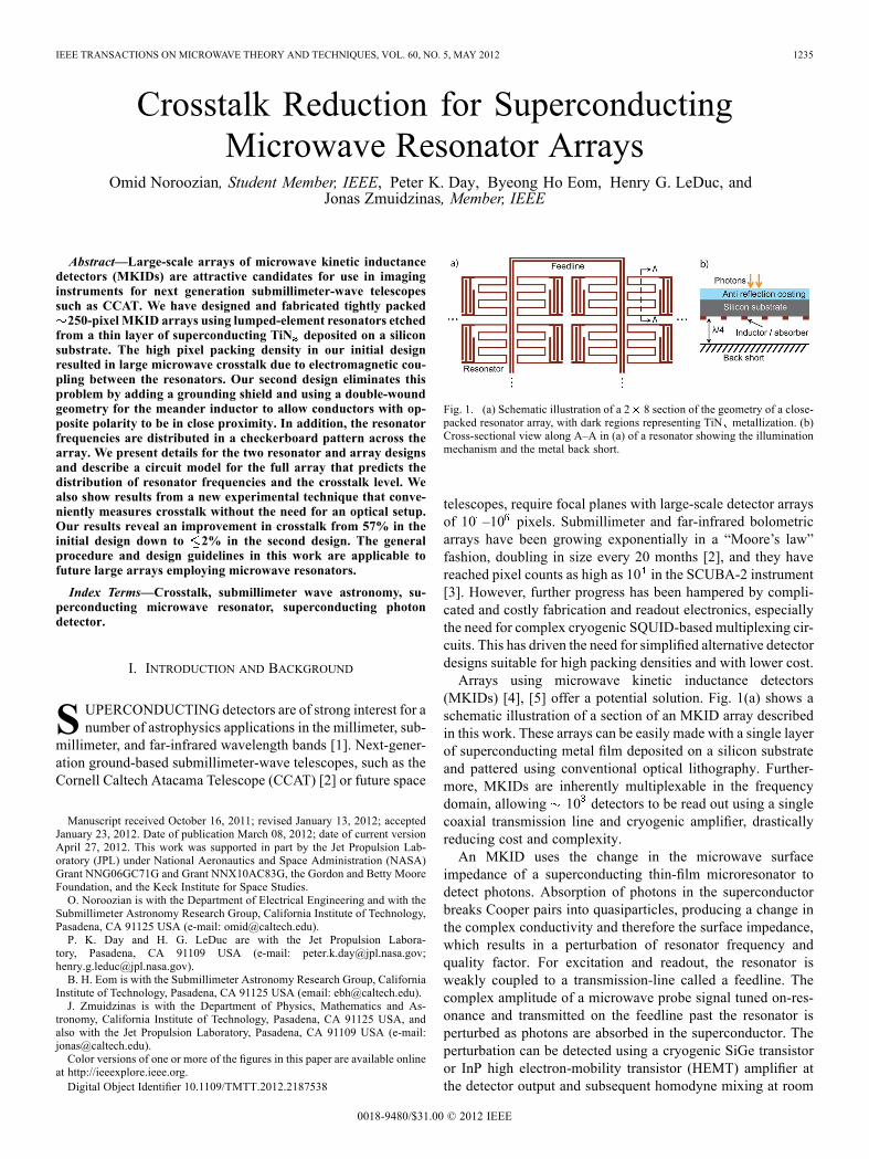
Fig. 1. (a) Schematic illustration of a 2 8 section of the geometry of a close-packed resonator array, with dark regions representing TiN metallization. (b)Cross-sectional view along A–A in (a) of a resonator showing the illuminationmechanism and the metal back short.
telescopes, require focal planes with large-scale detector arraysof 10 –10 pixels. Submillimeter and far-infrared bolometricarrays have been growing exponentially in a “Moore’s law”fashion, doubling in size every 20 months [2], and they havereached pixel counts as high as 10 in the SCUBA-2 instrument[3]. However, further progress has been hampered by compli-cated and costly fabrication and readout electronics, especiallythe need for complex cryogenic SQUID-based multiplexing cir-cuits. This has driven the need for simplified alternative detectordesigns suitable for high packing densities and with lower cost.Arrays using microwave kinetic inductance detectors
(MKIDs) [4], [5] offer a potential solution. Fig. 1(a) shows aschematic illustration of a section of an MKID array describedin this work. These arrays can be easily made with a single layerof superconducting metal film deposited on a silicon substrateand pattered using conventional optical lithography. Further-more, MKIDs are inherently multiplexable in the frequencydomain, allowing 10 detectors to be read out using a singlecoaxial transmission line and cryogenic amplifier, drasticallyreducing cost and complexity.An MKID uses the change in the microwave surface
impedance of a superconducting thin-film microresonator todetect photons. Absorption of photons in the superconductorbreaks Cooper pairs into quasiparticles, producing a change inthe complex conductivity and therefore the surface impedance,which results in a perturbation of resonator frequency andquality factor. For excitation and readout, the resonator isweakly coupled to a transmission-line called a feedline. Thecomplex amplitude of a microwave probe signal tuned on-res-onance and transmitted on the feedline past the resonator isperturbed as photons are absorbed in the superconductor. Theperturbation can be detected using a cryogenic SiGe transistoror InP high electron-mobility transistor (HEMT) amplifier atthe detector output and subsequent homodyne mixing at room
0018-9480/$31.00 © 2012 IEEE
1236 IEEE TRANSACTIONS ON MICROWAVE THEORY AND TECHNIQUES, VOL. 60, NO. 5, MAY 2012
temperature [4]. In an array of MKIDs, all the resonators arecoupled to a shared feedline and are tuned to slightly differentfrequencies. They can be read out simultaneously using a combof frequencies generated and measured using digital techniques[6], [7].MKID arrays are being developed for astronomy at a
wide range of wavelengths from millimeter waves to X-rays[7]–[10]. Other applications of superconducting resonatorsare in quantum computation experiments [11]–[13], multi-plexed readout of transition edge sensor bolometers [14], andparametric amplifiers [15]. Our previous work on mm/sub-millimeter-wave detection using MKIDs resulted in theconstruction and demonstration of a nearly complete imaginginstrument known as MUSIC (Multiwavelength SubmillimeterKinetic Inductance Camera) [7]. The focal plane has 576 spatialpixels. For each pixel, radiation is coupled onto the chip usinga planar multi-slot antenna and a low-loss superconductingNb microstrip feed network. Superconducting lithographicband-pass filters split the mm/submillimeter signal from everyantenna into four bands (850, 1100, 1300, and 2000 m), andthe radiation is then detected using one MKID resonator perband. Each resonator is a hybrid of an interdigitated capacitorand a coplanar waveguide (CPW) inductor mainly made fromNb, except for a short Al section at the end of the CPW. Thecoupled radiation is absorbed in the Al section of the resonatorswhich has a lower superconducting energy gap than the incidentmillimeter/submillimeter radiation energy. Fabrication of thearray requires approximately six levels of lithography. In June2010 a demonstration run of a prototype instrument resultedin encouraging results with sensitivities reaching close to thebackground noise limit [8].The arrays described in the present work are very different
from the MUSIC arrays. Since the new arrays are intended foroperation at a free-space wavelength of 350 m (860 GHz),Nb multi-slot antennas and microstriplines cannot be used as aradiation coupling mechanism due to the resistive loss above theNb superconducting energy gap ( 700 GHz). To demonstratethe feasibility of large arrays of submillimeter-wave MKIDs at350 m, we fabricated arrays with 250 resonators using varia-tions of Cardiff-style lumped-element resonators [16], [17]. Theresonator structures were designed to act as direct absorbersof radiation, taking advantage of highly resistive TiN films[18] to achieve a good impedance match to the incoming ra-diation. The TiN film is deposited on a high-resistivity crys-talline silicon substrate. The array is back-illuminated; the pho-tons travel through the substrate and are absorbed in the TiNresonators on the back side [see Fig. 1(b)]. Fresnel reflectionof radiation entering the silicon substrate can be eliminated byusing an anti-reflection layer. We demonstrated the basic oper-ation of the first-generation arrays by measuring the responseto a 215 m bandpass-filtered blackbody source, withthe results indicating 70% absorption efficiency (single polar-ization), comparable to the front/back power division ratio ex-pected for silicon. It should be possible to reach 100% by usinga metal backshort [19].Although the optical response measurements for our initial
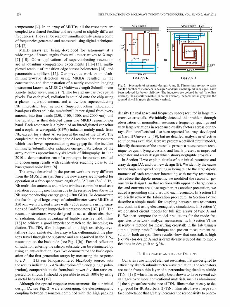
design (A; see Fig. 2) were encouraging, the electromagneticcoupling between resonators combined with the high packing
Fig. 2. Schematic of resonator designs A and B. Dimensions are not to scaleand the number of meanders in design A and turns in the spiral in design B havebeen reduced for better visibility. The inductors are colored in red (in onlineversion), the capacitors in blue (in online version), the feedlines in gray, and theground shield in green (in online version).
density (in real space and frequency space) resulted in large mi-crowave crosstalk. We initially detected this problem throughobservation of nonuniform resonance frequency spacings andvery large variations in resonance quality factors across our ar-rays. Similar effects had also been reported for arrays developedat Cardiff University [19], but no detailed analysis or effectivesolution was available. Here we present a detailed circuit model,identify the source of the crosstalk, present a measurement tech-nique for quantifying crosstalk, and finally present an improvedresonator and array design which shows negligible crosstalk.In Section II we explain details of our initial resonator and
array design (A), and our new design (B). We identify the causefor the high inter-pixel coupling as being due to the large dipolemoment of each resonator interacting with nearby resonators.To reduce the dipole moments, we modified the resonator ge-ometry in design B so that sections with opposite charge densi-ties and currents are close together. As another precaution, weadded a grounding shield around each resonator. In Section IIIwe briefly review the fabrication procedure. In Section IV wedescribe a simple model for coupling between two resonatorsand confirm it using electromagnetic simulations. In Section Vwe construct circuit models for full size arrays of type A andB. We then compare the model predictions for the mode fre-quencies to network analyzer measurements. In Section VI wedescribe a method for measuring crosstalk in the lab using asimple “pump-probe” technique and present measurement re-sults for both arrays. These results show that crosstalk is high( 57%) for design A and is dramatically reduced due to modi-fications in design B to 2%.
II. RESONATOR AND ARRAY DESIGNS
Our arrays use lumped element resonators that are designed toefficiently absorb submillimeter-wave radiation. The resonatorsare made from a thin layer of superconducting titanium nitride(TiN [18]) which has recently been shown to have several ad-vantages over more conventional materials such as aluminum:1) the high surface resistance of TiN films makes it easy to de-sign good far-IR absorbers; 2) TiN films also have a large sur-face inductance that greatly increases the responsivity to photo-
NOROOZIAN et al.: CROSSTALK REDUCTION FOR SUPERCONDUCTING MICROWAVE RESONATOR ARRAYS 1237
generated quasiparticles; 3) the high kinetic inductance also re-duces the resonance frequency, thereby increasing the multi-plexing density; 4) the ultra-low microwave loss in the materialenables extremely high quality factors as high as 3 10 [18];and 5) the transition temperature is tunable over a wide range( ) by changing the nitrogen content, which al-lows for optimization of the detector response over a wide rangeof loading conditions. For these reasons TiN is an excellentchoice for our detectors.Our initial resonator and array design (A) showed good op-
tical absorption properties but suffered from large crosstalk be-tween adjacent resonators. To solve this problem we created anew design (B). The two designs are explained below.
A. Design “A”
This design closely follows the original Cardiff proposal[16]: we use a lumped element resonator with a meanderedsingle-line inductor and an interdigitated capacitor (IDC). Aschematic of the resonator is shown in Fig. 2(a) and a photo-graph in Fig. 3(c). The whole resonator array is made from asingle layer of 40-nm-thick TiN film with transition tempera-ture K, sheet (kinetic) inductance pH, andsheet resistance 20 .The inductor is the photosensitive portion of the resonator
since the microwave current is large, whereas the capacitorelectrodes have much lower current and therefore this portionof the structure is essentially “blind”. The inductor consistsof 32 1-mm-long strips with a width of m and aspacing of m. The total inductance is nHat 1.5 GHz, and kinetic inductance fraction . Thekinetic inductance fraction is defined as the ratio of kineticinductance to total inductance of the line. The total size ofthe pixel is 1 mm 1 mm. We used an initial estimate for
to select the fill factor needed to achieve efficientsubmillimeter absorption. The relevant impedance-matchingcondition is given by
(1)
where is the dielectric constant of silicon in thefar-infrared at 1.5 K [20].The capacitor has four 0.9 mm 10 m fingers with rela-
tively large 10- m gaps to reduce two-level system noise anddissipation [21]. The capacitor area is kept to 10% of thetotal area in order to minimize dead space. The length of thecapacitor fingers can be varied to tune the resonance frequen-cies in the array. At maximum finger length, the capacitance is
pF. The coupling to the feedline was designed for acoupling quality factor .We fabricated a 16 14 array of these resonators. Readout
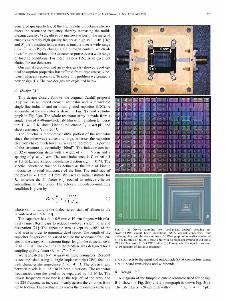
is accomplished using a single coplanar strip (CPS) feedlinewith characteristic impedance . The physical gapbetween pixels is 65 m in both directions. The resonatorfrequencies were designed to be separated by 1.3 MHz. Thelowest frequency resonator is at the top left of the array andthe 224 frequencies increase linearly across the columns fromtop to bottom. The feedline runs across the resonators vertically
Fig. 3. (a) Device mounting box (gold-plated copper) showing mi-crostrip-CPW circuit board transitions, SMA coaxial connectors, fourretaining clips, and the detector array. (b) Photograph of an earlier version ofa 16 16 array of design B pixels but with no resonator ground shield and aCPS feedline instead of a CPW feedline. (c) Photograph of design A resonator.(d) Photograph of design B resonator.
and connects to the input and output side SMA connectors usingcircuit board transitions and wirebonds.
B. Design “B”
A diagram of the lumped-element resonator used for designB is shown in Fig. 2(b) and a photograph is shown Fig. 3(d).The TiN film is 20 nm thick with K, pH,
1238 IEEE TRANSACTIONS ON MICROWAVE THEORY AND TECHNIQUES, VOL. 60, NO. 5, MAY 2012
and . The inductor is a coplanar strip (CPS) withm strips and m gap. The spacing between each
CPS pair is m. The inductor has a total inductance ofpH at 1.5 GHz, and . The total size of the
pixel is 0.65 mm 0.5 mm. The ratio has been tunedusing (1), where we have used an effective widthinstead of . The spiral shape was chosen to allow absorptionin both polarizations [22]. The efficiency of the absorber hasbeen simulated and measured and will be presented in a separatereport.The capacitor has fourteen 0.5 mm 5 m fingers with 5- m
gaps. The increased number of fingers allows for wider fre-quency tunability and better current uniformity in the inductor.At maximum finger length, the capacitance is pF. Thecoupling to the feedline was designed for .We fabricated a 16 16 array of these resonators [see
Fig. 3(b)] and used a finite-ground coplanar waveguide (CPW)feedline ( ) as opposed to a CPS feedline. We addedperiodic grounding straps connecting CPW ground strips toeliminate the unwanted coupled slotline mode [23]. We usedNb instead of TiN for the CPW centerline in order to reducethe impedance mismatch to the 50 connections, helpingto reduce the observed variability across the array. Thephysical gap spacing between pixels is 35 m in both di-rections. To further reduce crosstalk, the resonator frequenciesare split into two groups of 128: a high frequency band ( )and a low frequency band ( ) that are separated by 100 MHz,and are distributed in a checkerboard pattern in the array. Thefrequency spacing between resonances was designed to be 1.25and 2.2 MHz in the - and -bands, respectively. Startingfrom the top left and going down in the first column, we haveresonator (the lowest frequency in the -band), (lowestin the -band), . In the second column wehave , etc. This pattern distributes the resonators ina way that keeps resonators that are close in frequency fartherapart physically, reducing the pixel–pixel crosstalk.As will be shown in Sections V and VI, design B has consid-
erably lower crosstalk than design A. In design B the use of adouble-wound (CPS) inductor places conductors with oppositepolarities in close physical proximity, resulting in a good degreeof cancellation of the resonator’s electromagnetic fields. Thisconfines the fields closer to the structure, reducing stray inter-actions between nearby resonators in a close-packed array. Thegrounding shield around each resonator further helps in con-fining the fields. As a positive side effect of the proximity ofopposite polarity conductors, the geometrical inductance in de-sign B is reduced resulting in a larger . A theoretical circuitmodel and experimental crosstalk results for design A and B arediscussed in Sections IV–VI.
III. FABRICATION PROCEDURE
First, a layer of TiN film is sputtered onto an ambient-tem-perature, high-resistivity ( k cm) silicon substrate.The substrate is cleaned with hydrofluoric acid (HF) prior to de-position. The critical temperature of the film is sensitive tothe stoichiometry of the film and is controlled by the flow rateof the sputtering gases Ar and N [18]. UV projection lithog-raphy is used followed by inductively coupled plasma etching
using BCl /Cl to pattern the resonator structures and the CPSfeedline, all in one layer, for design A.For design B the feedline is a CPW line with periodic TiN
ground straps spaced 500 m apart. To avoid shorts causedby the straps, the centerline is initially not patterned and a200-nm-thick insulating layer of SiO is deposited on topusing RF magnetron sputtering from a high purity fused silicatarget. A thin layer of niobium is then deposited using dcmagnetron sputtering, and is patterned using an inductivelycoupled plasma etcher and a mixture of CCl F , CF , and O ,to create the centerline of the CPW feedline. The SiO layer isthen patterned using a buffered oxide etch (BOE) to removeSiO from over the resonators.
IV. COUPLED-RESONATORS MODEL
A simple circuit can be used to model electromagnetic cou-pling between two adjacent resonators in our arrays. The cou-pling can be capacitive, inductive, or a combination of the two.For purposes of discussion we assume a net capacitive coupling.Fig. 4(a) shows two resonators coupled with a cross-couplingcapacitor , with and being the capacitances of the in-terdigitated capacitors (IDC) and . (If the cou-pling were inductive, would be replaced by an inductor
where and a similar analysis as explained belowwould follow). The inductor represents inductance of the me-andered lines in design A and the spiral in design B resonators. Itis easy to see that if the two resonators are uncoupled ( ),the two natural resonance modes are ,,2. However, if , the frequencies of the two modes are
(2)
where the capacitance eigenvalues are
(3)
and where and . Thevalues for , , and can be extracted by simulating eachcomponent in an electromagnetic (EM) simulation software likeSonnet [24]. The value of the coupling element ( or ) isdifficult to extract from direct simulation. However, by exam-ining the details of the above circuit, one can see that in a casewhere , the eigenvectors are either(“symmetric mode”) or (“anti-symmetric mode”).We define the splitting frequency and
where and refer to the symmetric and anti-symmetric mode frequencies. Depending on the type of cross-coupling, for capacitive coupling (as in Fig. 4) and
for inductive coupling. From this, it is easy to showthat
for capacitive coupling (4)
for inductive coupling (5)
These equations allow us to determine the value of the couplingelement assuming that we know . The quantity is
NOROOZIAN et al.: CROSSTALK REDUCTION FOR SUPERCONDUCTING MICROWAVE RESONATOR ARRAYS 1239
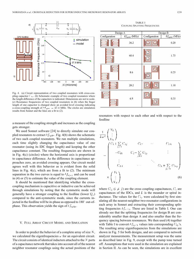
Fig. 4. (a) Circuit representation of two coupled resonators with cross-cou-pling capacitor . (b) Schematic example of two coupled resonators wherethe length difference of the capacitors is indicated. Dimensions are not to scale.(c) Resonance frequencies of two coupled resonators in (b) when the fingerlength of one capacitor is changed show an avoided level crossing indicatinga cross-coupling strength of MHz. The circles are simulationresults from Sonnet and the lines are a fit to (2).
a measure of the coupling strength and increases as the couplinggets stronger.We used Sonnet software [24] to directly simulate our cou-
pled resonators to extract . Fig. 4(b) shows the schematicof two such coupled resonators. We run multiple simulations,each time slightly changing the capacitance value of oneresonator (using its IDC finger length) and keeping the othercapacitance constant. The resulting frequencies are shown inin Fig. 4(c) (circles) where the horizontal axis is proportionalto capacitance difference. As the difference in capacitance ap-proaches zero, an avoided crossing appears. Our circuit modelagrees well with this behavior as is evident from the solidlines in Fig. 4(c), which are from a fit to (2). The minimumseparation in the two curves is equal to and can be usedin (4) or (5) to estimate the value of the coupling element.It should be mentioned that identifying whether the cross-
coupling mechanism is capacitive or inductive can be achievedthrough simulations by noting that the symmetric mode willgenerally have a stronger coupling to the feedline (lower )compared to the anti-symmetric mode, since the currents in-jected in the feedline will be in-phase as opposed to 180 out-of-phase. This observation yields the sign of .
V. FULL ARRAY CIRCUIT MODEL AND SIMULATION
In order to predict the behavior of a complete array of size ,we calculated the eigenfrequencies for an equivalent circuit.The circuit consists of identical inductors attached to the portsof a capacitance network that takes into account all of the nearestneighbor resonator couplings using the actual positions of the
TABLE ICOUPLING SPLITTING FREQUENCIES
resonators with respect to each other and with respect to thefeedline
...
...
.... . .
... (6)
where ( ) are the cross coupling capacitances, arecapacitances of the IDCs, and is the meander or spiral in-ductance. The values for the were calculated by first sim-ulating all the nearest-neighbor two-resonator configurations ineach array in Sonnet and extracting their corresponding split-ting frequencies . These are listed in Table I. One canalready see that the splitting frequencies for design B are con-siderably smaller than design A and also smaller than the fre-quency spacing between resonances. We then used (4) togetherwith Table I to convert values into corresponding ’s.The resulting array eigenfrequencies from the simulations areshown in Fig. 5 for both designs, and are compared to networkanalyzer measurements. The measurement setup was the sameas described later in Fig. 9, except with the pump tone turnedoff. Assumptions that were used in the simulation are explainedin Section II. As can be seen, the simulations are in excellent

1240 IEEE TRANSACTIONS ON MICROWAVE THEORY AND TECHNIQUES, VOL. 60, NO. 5, MAY 2012
Fig. 5. Measurements of array resonance frequencies for both designs A and Band comparison to simulation. The two “simulation (no coupling)” curves arefor when .
Fig. 6. Series of simulations showing how the frequency curve shape evolvesas the coupling strength is varied by tuning the scaling factor .
agreement with measurements for both arrays, confirming ourcircuit model for coupled resonator arrays.The specific inverted- -shape of the curve for design A is a
characteristic feature of highly coupled arrays. This has beenfurther explored in Fig. 6 where we have plotted the eigen-frequencies for design A for a range of coupling strengths byscaling the values in Table I by the same factor. As can be seen,the -shape gradually disappears as we reduce the strength ofthe coupling, and becomes negligible by the time it is down bya factor of 16. The same -shape eventually also appears inboth bands of array B when we artificially scale up the couplingstrength, but for the actual array the effect is negligible thanksto the much smaller splitting frequencies and the checkerboardfrequency scheme.Equation (6) also yields the normalized eigenvectors for the
resonance modes. An example is shown visually in Fig. 7 whereit can be seen that the mode is highly delocalized for design Awhereas it is highly localized for design B. The colors showthe amount of normalized energy contributed by each physical
Fig. 7. Normalized energy (20 ) in voltages to across thearray for a specificmode number (#68) in both arrays is shown in color (in onlineversion). In an uncoupled array, this mode number would purely correspondto the resonator in position # 68 in array A, and in position # 135 in array B(indicated by arrows). However, due to strong coupling in array A, energy isdistributed over many resonators, while in array B the energy is well localized.
resonator to the resonance mode. The energy in each of thefour diagonal nearest neighbor pixels in design B is more than40 dB lower than the main pixel. These results strongly indicatethat crosstalk is dramatically reduced in design B. This conclu-sion is confirmed by direct measurements and simulations of thecrosstalk, which we present in Section VI.
VI. CROSSTALK
One method to measure crosstalk is to illuminate a singlephysical resonator on the array with submillimeter photons andto look for a response in other resonances. This approach is dif-ficult because confining the far-IR light to one pixel requires acomplicated optical setup. Instead, we developed a very simple“pump-probe” technique where we apply a microwave “pump”tone to a resonance and observe the response from the other res-onances. This technique exploits the fact that the kinetic induc-tance of a superconductor generally is nonlinear [5], [25] andcan change as a function of the microwave current
(7)
where is the microwave current in the inductor, and setsthe scale of the nonlinearity and is often comparable to the DCcritical current. By applying a strong microwave pump tone toone of the resonance modes with frequency , the microwavecurrents in the inductors that participate in that mode cause theinductance values to increase slightly according to (7), so themode frequency decreases to a new value that may be char-acterized by the frequency shift . In an arraywhere the pixels are coupled, this will also result in shifts inother modes, and by comparing these shifts to we can exper-imentally measure crosstalk for each mode. If and are thefrequency of a certain “probed” mode when the pump is ap-plied on-resonance and off-resonance respectively, then a quan-titative measure of the crosstalk may be defined as
. The effect of the nonlinearity-induced shifts inthe inductances may be analyzed by generalizing (6) to includenon-equal inductors, and by noting that in ourmeasurements so the use of linear perturbation theory is very

NOROOZIAN et al.: CROSSTALK REDUCTION FOR SUPERCONDUCTING MICROWAVE RESONATOR ARRAYS 1241
Fig. 8. Crosstalk simulations for full-size arrays A and B. In both simulationsmode number 68 (indicated in red, in online version) is pumped. By definition,crosstalk for the pumped mode is 100%. Note that the scales are very differentin the two plots.
well justified. The result of this calculation yields an expressionfor the crosstalk values
(8)
Here and are the voltage eigenvector components formodes and in our circuit model (Fig. 7). This result demon-strates that modes whose “energy overlap” is large will havesignificant crosstalk.Fig. 8 shows crosstalk simulated for both arrays A and B
using (8). In both simulations an arbitrary mode number (#68)was pumped. The simulations show that crosstalk is very high indesign A (up to 75%) where many other modes are affected bythe pump, while in design B there is almost no crosstalk downto a level of 0.04%.The measurement setup is illustrated in Fig. 9 where a syn-
thesizer provides microwave power (pump) at the frequencyof one of the resonance modes ( ). All the resonances wereprobed using a network analyzer in a relatively low power mode( 100 dBm on the feedline), so that the pump power wasdominant ( 80 dBm).Crosstalk measurement results are shown in
Fig. 10(a) and (b). Both plots are for a group of reso-nances that have frequencies not too far from the pumpedresonance. Fig. 10(a) clearly shows that design A is dominatedby crosstalk as large as 57%. Fig. 10(b) shows that by going todesign B, crosstalk dramatically reduces down to a maximumof 2%. The error bars are a result of the fits to the resonancesby a fitting code [27] used to fit the data from the networkanalyzer. Because the network analyzer scans were taken atrelatively low power, higher measurement times were requiredwhich made the data susceptible to various noise sourcesincluding network analyzer frequency drift and magneticfields affecting the resonance positions [28]. The simulationsshown in Fig. 8 support the measurements and suggest thatthe actual crosstalk in design B could be much lower than theexperimental upper limit of 2%.
Fig. 9. Illustration of the setup for measuring the resonances and the crosstalk.The resonators are cooled down to below 100 mK in a cryogenic refrigerator,and are read out using a network analyzer. An SiGe transistor amplifier [26]at 4 K is used to amplify the signal. The synthesizer pump power is combinedwith readout power using a 3-dB power combiner. The pump signal frequency istuned on a resonance (blue curve in online version) which causes the resonanceto shift (red curve in online version). A nearby coupled resonance also shifts asa result.
Fig. 10. Crosstalk measurement results for designs A and B. The (frequency)position of the pumped resonance is shown by the dashed line. The red bars (inonline version) indicate the measurement error.
VII. SUMMARY
We successfully fabricated 250-pixel arrays of submil-limeter-wave MKIDS using TiN on silicon. We demonstratedthe basic operation of these arrays by measuring their responseto a blackbody source. However, the arrays suffered from
1242 IEEE TRANSACTIONS ON MICROWAVE THEORY AND TECHNIQUES, VOL. 60, NO. 5, MAY 2012
crosstalk between individual pixels due to large resonatordipole moments interacting with nearby resonators. We devel-oped a simple and general circuit model that accounts for thecrosstalk and agrees well with measurements of the array fre-quency curve patterns and crosstalk. We created a new designthat eliminates crosstalk in two ways: 1) by reducing the dipolemoment of each resonator and 2) by distributing the resonatorsacross the array in a checkerboard pattern. We developed asimple “pump-probe” technique to directly measure crosstalk,and showed that crosstalk in design B is indeed smaller and isdramatically reduced to 2%. The general procedure and de-sign guidelines in this work are applicable to future large-scalearrays of microwave resonators for telescopes like CCAT.
ACKNOWLEDGMENT
The authors would like to thank S. Golwala, D. Moore,L. Swenson, and R. Duan with the California Institute of Tech-nology, Pasadena, for helpful discussions. The devices used inthis work were fabricated at the JPL Microdevices Laboratory,Pasadena, CA.
REFERENCES[1] J. Zmuidzinas and P. L. Richards, “Superconducting detectors and
mixers for millimeter and submillimeter astrophysics,” Proc. IEEE,vol. 92, no. 10, pp. 1597–1616, Oct. 2004.
[2] “Panel reports—New worlds, new horizons in astronomy and astro-physics,” National Research Council, Washington, DC, 2011. [Online].Available: http://www.nap.edu/catalog.php?record_id=12982
[3] W. S. Holland, W. D. Duncan, B. D. Kelly, K. D. Irwin, A. J. Walton,P. A. R. Ade, and E. I. Robson, “SCUBA-2: A large format submil-limetre camera on the James Clerk Maxwell Telescope,” in Proc. SPIEMillimeter Submillimeter Detectors Astron. Conf., 2003, vol. 4855, pp.1–18.
[4] P. K. Day, H. G. LeDuc, B. A. Mazin, A. Vayonakis, and J. Zmuidz-inas, “A broadband superconducting detector suitable for use in largearrays,” Nature, vol. 425, no. 6960, pp. 817–821, Oct. 2003.
[5] J. Zmuidzinas, “Superconducting microresonators: Physics and appli-cations,” Annu. Rev. Cond. Mat. Phys., vol. 3, pp. 169–214, 2012.
[6] B. A. Mazin, P. K. Day, K. D. Irwin, and C. D. Reintsema, “Dig-ital readouts for large microwave low-temperature detector arrays,”Nuclear Instrum. Methods Phys. Res.—Sec. A, vol. 599, no. 2, pp.799–801, Apr. 2006.
[7] P. R.Maloney, N. G. Czakon, P. K. Day, T. P. Downes, R. Duan, J. Gao,J. Glenn, S. R. Golwala, M. I. Hollister, H. G. Leduc, B. A. Mazin, O.Noroozian, H. T. Nguyen, J. Sayers, J. A. Schlaerth, S. Siegel, J. E.Vaillancourt, A. Vayonakis, P. R. Wilson, and J. Zmuidzinas, “MUSICfor sub/millimeter astrophysics,” in Proc. SPIE Millimeter, Submil-limeter, Far-Infrared Detectors Instrum. Astron. V Conf., 2010, vol.7741, Art. ID 77410F.
[8] J. A. Schlaerth, J. Glenn, P. R. Maloney, N. G. Czakon, T. P. Downes,R. Duan, S. R. Golwala, M. I. Hollister, O. Noroozian, S. Siegel, A.Vayonakis, J. P. Zmuidzinas, K. Day, H. G. LeDuc, H. T. Nguyen,J. Sayers, P. R. Wilson, J. Gao, B. A. Mazin, and J. E. Vaillancourt,“MKID multicolor array status and results from DemoCam,” in Proc.SPIE Millimeter, Submillimeter, Far-Infrared Detectors Instrum. As-tron. V Conf., 2010, vol. 7741, Art. ID 774109.
[9] B. A. Mazin, K. O’Brien, S. McHugh, B. Bumble, D. Moore, S. Gol-wala, and J. Zmuidzinas, “ARCONS: A highly multiplexed supercon-ducting optical to near-IR camera,” in Proc. SPIE Ground-Based Air-borne Instrum. Astron. III Conf., 2010, vol. 7735, Art. ID 773518.
[10] A. Monfardini, A. Benoit, A. Bideaud, L. J. Swenson, M. Roesch, F.X. Desert, S. Doyle, A. Endo, A. Cruciani, P. Ade, A. M. Baryshev,J. J. A. Baselmans, O. Bourrion, M. Calvo, P. Camus, L. Ferrari, C.Giordano, C. Hoffmann, S. Leclercq, J. F. Macias-Perez, P. Mauskopf,K. F. Schuster, C. Tucker, C. Vescovi, and S. J. C. Yates, “A dual-band millimeter-wave kinetic inductance camera for the IRAM 30 mtelescope,” Astrophys. J. Suppl. Ser., vol. 194, Jun. 2011, Art. ID 24.
[11] J. B. Hertzberg, T. Rocheleau, T. Ndukum, M. Savva, A. A. Clerk, andK. C. Schwab, “Back-action-evading measurements of nanomechan-ical motion,” Nature Phys., vol. 6, no. 3, pp. 213–217, Mar. 2010.
[12] J. Koch, A. A. Houck, K. Le Hur, and S. M. Girvin, “Time-reversal-symmetry breaking in circuit-QED-based photon lattices,” Phys. Rev.A, Gen. Phys., vol. 82, no. 4, Oct. 2010, Art. ID 043811.
[13] C. M. Wilson, T. Duty, M. Sandberg, F. Persson, V. Shumeiko, and P.Delsing, “Photon generation in an electromagnetic cavity with a time-dependent boundary,”Phys. Rev. Lett., vol. 105, no. 23, Dec. 2010, Art.ID 233907.
[14] J. A. B.Mates, G. C. Hilton, K. D. Irwin, L. R. Vale, and K.W. Lehnert,“Demonstration of a multiplexer of dissipationless superconductingquantum interference devices,” Appl. Phys. Lett., vol. 92, no. 2, Jan.2008, Art. ID 023514.
[15] E. A. Tholen, A. Ergul, E. M. Doherty, F. M. Weber, F. Gregis, andD. B. Haviland, “Nonlinearities and parametric amplification in super-conducting coplanar waveguide resonators,” Appl. Phys. Lett., vol. 90,no. 25, Jun. 2007, Art. ID 253509.
[16] S. Doyle, P. Mauskopf, J. Naylon, A. Porch, and C. Duncombe,“Lumped element kinetic inductance detectors,” J. Low Temp. Phys.,vol. 151, pp. 530–536, Apr. 2008.
[17] O. Noroozian, P. K. Day, B. H. Eom, H. G. Leduc, and J. Zmuidz-inas, “Microwave crosstalk in lumped element far-IR MKIDs,” pre-sented at the Proc. 35th Int. Conf. Infrared Millimeter Terahertz Waves(IRMMW-THz), Rome, Italy, 2010.
[18] H. G. Leduc, B. Bumble, P. K. Day, A. D. Turner, B. H. Eom, S. Gol-wala, D. C. Moore, O. Noroozian, J. Zmuidzinas, J. Gao, B. A. Mazin,S. McHugh, and A. Merrill, “Titanium nitride films for ultrasensitivemicroresonator detectors,” Appl. Phys. Lett., vol. 97, no. 10, Sep. 2010,Art. ID 102509.
[19] S. Doyle, P. Mauskopf, J. Zhang, S. Withington, D. Goldie, D.Glowacka, A. Monfardini, L. Swenson, and M. Roesch, “Optimisationof lumped element kinetic inductance detectors for use in groundbased mm and sub-mm arrays,” in Proc. AIP Conf., 2009, vol. 1185,pp. 156–159.
[20] J. W. Lamb, “Miscellaneous data on materials for millimetre and sub-millimetre optics,” Int. J. Infrared Millimeter Waves, vol. 17, no. 12,pp. 1997–2034, Dec. 1996.
[21] O. Noroozian, J. S. Gao, J. Zmuidzinas, H. G. Leduc, and B. A. Mazin,“Two-level system noise reduction for Microwave Kinetic InductanceDetectors,” in Proc. AIP 13th Int. Workshop Low Temp. Detectors,2009, vol. 1185, pp. 148–151.
[22] A. Brown, W. Hsieh, S. H. Moseley, T. R. Stevenson, K. U-yen, andE. J. Wollack, “Fabrication of an absorber-coupled MKID detector andreadout for sub-millimeter and far-infrared astronomy,” in Proc. SPIEMillimeter, Submillimeter, Far-Infrared Detectors Instrum. Astron. VConf., 2010, vol. 7741, Art. ID 77410P.
[23] G. E. Ponchak, J. Papapolymerou, and M. M. Tentzeris, “Excitationof coupled slotline mode in finite-ground CPW with unequal ground-plane widths,” IEEE Trans. Microw. Theory Tech., vol. 53, no. 2, pp.713–717, Feb. 2005.
[24] Sonnet Softw. Inc. North Syracuse, NY, 2011. [Online]. Available:http://www.sonnetusa.com/
[25] T. Dahm and D. J. Scalapino, “Theory of intermodulation in a super-conducting microstrip resonator,” J. Appl. Phys., vol. 81, no. 4, pp.2002–2209, Feb. 1997.
[26] S. Weinreb, J. Bardin, H. Mani, and G. Jones, “Matched wideband low-noise amplifiers for radio astronomy,” Rev. Sci. Instrum., vol. 80, no.4, Apr. 2009, Art. ID 044702.
[27] J. Gao, “The physics of superconducting microwave resonators,” Ph.D.dissertation, Dept. Phys., California Inst. Tech., Pasadena, CA, 2008.
[28] J. E. Healey, T. Lindstrom, M. S. Colclough, C. M. Muirhead, andA. Y. Tzalenchuk, “Magnetic field tuning of coplanar waveguide res-onators,” Appl. Phys. Lett., vol. 93, no. 4, Jul. 2008, Art. ID 043513.
Omid Noroozian (S’07) received the B.S. degree inelectronics engineering from the Sharif Universityof Technology, Tehran, Iran, in 2004, the M.Sc.degree in microelectronics from the Delft Universityof Technology (TUDelft), Delft, The Netherlands,in 2006, the M.S. degree in applied physics fromthe California Institute of Technology, Pasadena,in 2009, and is currently working toward the Ph.D.degree in electrical engineering at the CaliforniaInstitute of Technology.He was a Research Assistant with the Physics
of Nano-Electronics Group, Kavli Institute of Nanoscience, TUDelft, from2005 to 2006, where he worked on design and fabrication of superconductingtunnel junction heterodyne mixer chips for the atacama large millimeter array(ALMA) telescope. Since 2006, he has been a Research Assistant with the
NOROOZIAN et al.: CROSSTALK REDUCTION FOR SUPERCONDUCTING MICROWAVE RESONATOR ARRAYS 1243
Submillimeter Wave Astrophysics Group, California Institute of Technology,where he is working on development of kinetic inductance detector technologyfor large-scale submillimeter/far infrared arrays for the Caltech SubmillimeterObservatory (CSO) and the Cornell Caltech Atacama Telescope (CCAT).
Peter K. Day, photograph and biography not available at time of publication.
Byeong Ho Eom, photograph and biography not available at time of publica-tion.
Henry G. LeDuc, photograph and biography not available at time of publica-tion.
Jonas Zmuidzinas (M’91) received the B.S. degreein physics from the California Institute of Tech-nology, Pasadena, in 1981, and the Ph.D. degreein physics from the University of California atBerkeley, in 1987.He was a Postdoctoral Fellow in 1988–1989 at
the University of Illinois at Urbana-Champaign. Hejoined the physics faculty at the California Instituteof Technology in 1989, and currently serves as theMerle Kingsley Professor of Physics. He also has anappointment at the Jet Propulsion Laboratory (JPL),
California Institute of Technology, where he serves as JPL’s Chief Technologist.


![Microwave 06 [相容模式] - 國立中興大學web.nchu.edu.tw/~ycchiang/MicroWave/Microwave_06.pdf · j Lossless resonator 1 Resonator with loss: 0 0 R 0 Z in j2L 0 Q Q LC average](https://static.fdocuments.net/doc/165x107/605d15180e6d5c373672567b/microwave-06-c-oecewebnchuedutwycchiangmicrowavemicrowave06pdf.jpg)
