
IEEE TRANSACTIONS ON COMPUTER-AIDED...
13
IEEE TRANSACTIONS ON COMPUTER-AIDED DESIGN OF INTEGRATED CIRCUITS AND SYSTEMS, VOL. 37, NO. 4, APRIL 2018 729 Accelerating Dynamic Time Warping With Memristor-Based Customized Fabrics Xiaowei Xu, Student Member, IEEE, Feng Lin, Member, IEEE, Aosen Wang, Student Member, IEEE, Xinwei Yao, Member, IEEE, Qing Lu, Wenyao Xu, Member, IEEE, Yiyu Shi, Senior Member, IEEE, and Yu Hu, Member, IEEE Abstract—The rapid development of Internet of Things is yielding a huge volume of time series data, the real-time min- ing of which becomes a major load for data centers. The computation bottleneck in time series mining is the distance measure, in which dynamic time warping (DTW) is one of the most widely used distance measures. Recently, various soft- ware optimization and hardware acceleration techniques have been proposed for DTW acceleration. However, the throughput and energy efficiency of DTW are still big concerns consider- ing the ever-increasing volume of times series. In this paper, we propose a high-throughput and efficient memristor-based DTW architecture for real-time time series mining on data centers. Specifically, memristors have been adopted for both compu- tation and configuration of the computing architecture. The computation flow in this architecture is fully presented in a con- tinuous and asynchronous manner. To improve the computation efficiency, we propose an early lower bound algorithm by exploit- ing the predictability in the circuit characteristic. Experiments are performed with module evaluation and end-to-end evalua- tion including three popular applications: 1) similarity search; 2) classification; and 3) anomaly detection. Experimental results indicate that, compared to existing approaches, the speedup and energy efficiency improvement are 12×–43× and 51×–287×, respectively. Index Terms—Data mining, dynamic time warping (DTW), energy efficiency, high throughput, memristor, time series. Manuscript received January 27, 2017; revised April 25, 2017 and June 18, 2017; accepted June 21, 2017. Date of publication July 19, 2017; date of current version March 29, 2018. This paper was recommended by Associate Editor S. Pasricha. (Corresponding author: Yu Hu.) X. Xu is with the School of Optical and Electronic Information, Huazhong University of Science and Technology, Wuhan 430074, China, and also with the Department of Computer Science and Engineering, University of Notre Dame, Notre Dame, IN 46556 USA (e-mail: [email protected]). F. Lin, A. Wang, and W. Xu are with the Department of Computer Science and Engineering, State University of New York at Buffalo, Buffalo, NY 14260-2500 USA (e-mail: fl[email protected]; [email protected]; [email protected]). X. Yao is with the Department of Computer Science and Engineering, Zhejiang University of Technology, Hangzhou 310023, China (e-mail: [email protected]). Q. Lu and Y. Shi are with the Department of Computer Science and Engineering, University of Notre Dame, Notre Dame, IN 46556 USA (e-mail: [email protected]; [email protected]). Y. Hu is with the School of Optical and Electronic Information, Huazhong University of Science and Technology, Wuhan 430074, China (e-mail: [email protected]). Color versions of one or more of the figures in this paper are available online at http://ieeexplore.ieee.org. Digital Object Identifier 10.1109/TCAD.2017.2729344 I. I NTRODUCTION E NERGY efficiency of data centers has been a primary focus in the past a few years due to their excessive power consumption. On the other hand, the load on data centers keeps increasing with the explosion of information technolo- gies. It has been predicted that a major portion of the load will come from Internet of Things (IoT), which will yield over 4.4 zettabytes (5.5 × 10 21 Bytes) of time series data by 2020 [6]. These time series data are transmitted to data centers for real- time mining [20]. It is therefore of utmost interest to explore techniques that handle time series data in real-time with high energy efficiency. Distance measure between time series plays an important role in time series mining, which is the foundation of higher data mining tasks, such as classification and similarity search. Dynamic time warping (DTW) is one of the best distance measures according to a recent comparison study of several distance measures with 44 datasets [13]. It is widely used in different fields, such as speech recognition, financial analysis, and network traffic monitoring [12]. However, DTW has a quadratic time complexity, which is computation-expensive for huge data processing in data centers. DTW has been well optimized with software and hard- ware methods to solve the obstacle of computation complexity. Lower bound (LB) [14], [25] is a powerful optimization method, which can prune a lot of sequences in many tasks such as similarity search and classification. Early abandon [37] is also very effective. Rakthanmanon et al. [37] cascaded multiple stages of software optimizations, which is considered as the most powerful software implementation for similarity search to date. DTW in a streaming manner is proposed by Sakurai et al. [41], which achieves a linear time complexity, however, allows false dismissals. The majority of these tech- niques achieve speedup by reducing the number of the invoked times of DTW rather than accelerating DTW itself. However, DTW calculation still accounts for about 80% of the total executing time [48], [51]. Meanwhile, customized hardware is adopted for further acceleration. Sart et al. [42] proposed a highly pipelined archi- tecture for DTW on field-programmable gate arrays (FPGAs), which can compute DTW in linear time. Wang et al. [48] implemented a high-throughput DTW framework for similarity search on FPGAs. The proposed structure of processing ele- ment (PE) ring exploits the fine-grained parallelism of DTW 0278-0070 c 2017 IEEE. Personal use is permitted, but republication/redistribution requires IEEE permission. See http://www.ieee.org/publications_standards/publications/rights/index.html for more information.
Transcript of IEEE TRANSACTIONS ON COMPUTER-AIDED...

IEEE TRANSACTIONS ON COMPUTER-AIDED DESIGN OF INTEGRATED CIRCUITS AND SYSTEMS, VOL. 37, NO. 4, APRIL 2018 729
Accelerating Dynamic Time Warping WithMemristor-Based Customized Fabrics
Xiaowei Xu, Student Member, IEEE, Feng Lin, Member, IEEE, Aosen Wang, Student Member, IEEE,Xinwei Yao, Member, IEEE, Qing Lu, Wenyao Xu, Member, IEEE,
Yiyu Shi, Senior Member, IEEE, and Yu Hu, Member, IEEE
Abstract—The rapid development of Internet of Things isyielding a huge volume of time series data, the real-time min-ing of which becomes a major load for data centers. Thecomputation bottleneck in time series mining is the distancemeasure, in which dynamic time warping (DTW) is one ofthe most widely used distance measures. Recently, various soft-ware optimization and hardware acceleration techniques havebeen proposed for DTW acceleration. However, the throughputand energy efficiency of DTW are still big concerns consider-ing the ever-increasing volume of times series. In this paper, wepropose a high-throughput and efficient memristor-based DTWarchitecture for real-time time series mining on data centers.Specifically, memristors have been adopted for both compu-tation and configuration of the computing architecture. Thecomputation flow in this architecture is fully presented in a con-tinuous and asynchronous manner. To improve the computationefficiency, we propose an early lower bound algorithm by exploit-ing the predictability in the circuit characteristic. Experimentsare performed with module evaluation and end-to-end evalua-tion including three popular applications: 1) similarity search;2) classification; and 3) anomaly detection. Experimental resultsindicate that, compared to existing approaches, the speedup andenergy efficiency improvement are 12×–43× and 51×–287×,respectively.
Index Terms—Data mining, dynamic time warping (DTW),energy efficiency, high throughput, memristor, timeseries.
Manuscript received January 27, 2017; revised April 25, 2017 andJune 18, 2017; accepted June 21, 2017. Date of publication July 19, 2017;date of current version March 29, 2018. This paper was recommended byAssociate Editor S. Pasricha. (Corresponding author: Yu Hu.)
X. Xu is with the School of Optical and Electronic Information,Huazhong University of Science and Technology, Wuhan 430074, China,and also with the Department of Computer Science and Engineering,University of Notre Dame, Notre Dame, IN 46556 USA (e-mail:[email protected]).
F. Lin, A. Wang, and W. Xu are with the Department of ComputerScience and Engineering, State University of New York at Buffalo, Buffalo,NY 14260-2500 USA (e-mail: [email protected]; [email protected];[email protected]).
X. Yao is with the Department of Computer Science and Engineering,Zhejiang University of Technology, Hangzhou 310023, China (e-mail:[email protected]).
Q. Lu and Y. Shi are with the Department of Computer Science andEngineering, University of Notre Dame, Notre Dame, IN 46556 USA (e-mail:[email protected]; [email protected]).
Y. Hu is with the School of Optical and Electronic Information, HuazhongUniversity of Science and Technology, Wuhan 430074, China (e-mail:[email protected]).
Color versions of one or more of the figures in this paper are availableonline at http://ieeexplore.ieee.org.
Digital Object Identifier 10.1109/TCAD.2017.2729344
I. INTRODUCTION
ENERGY efficiency of data centers has been a primaryfocus in the past a few years due to their excessive power
consumption. On the other hand, the load on data centerskeeps increasing with the explosion of information technolo-gies. It has been predicted that a major portion of the load willcome from Internet of Things (IoT), which will yield over 4.4zettabytes (5.5× 10²¹ Bytes) of time series data by 2020 [6].These time series data are transmitted to data centers for real-time mining [20]. It is therefore of utmost interest to exploretechniques that handle time series data in real-time with highenergy efficiency.
Distance measure between time series plays an importantrole in time series mining, which is the foundation of higherdata mining tasks, such as classification and similarity search.Dynamic time warping (DTW) is one of the best distancemeasures according to a recent comparison study of severaldistance measures with 44 datasets [13]. It is widely used indifferent fields, such as speech recognition, financial analysis,and network traffic monitoring [12]. However, DTW has aquadratic time complexity, which is computation-expensive forhuge data processing in data centers.
DTW has been well optimized with software and hard-ware methods to solve the obstacle of computation complexity.Lower bound (LB) [14], [25] is a powerful optimizationmethod, which can prune a lot of sequences in many taskssuch as similarity search and classification. Early abandon [37]is also very effective. Rakthanmanon et al. [37] cascadedmultiple stages of software optimizations, which is consideredas the most powerful software implementation for similaritysearch to date. DTW in a streaming manner is proposed bySakurai et al. [41], which achieves a linear time complexity,however, allows false dismissals. The majority of these tech-niques achieve speedup by reducing the number of the invokedtimes of DTW rather than accelerating DTW itself. However,DTW calculation still accounts for about 80% of the totalexecuting time [48], [51].
Meanwhile, customized hardware is adopted for furtheracceleration. Sart et al. [42] proposed a highly pipelined archi-tecture for DTW on field-programmable gate arrays (FPGAs),which can compute DTW in linear time. Wang et al. [48]implemented a high-throughput DTW framework for similaritysearch on FPGAs. The proposed structure of processing ele-ment (PE) ring exploits the fine-grained parallelism of DTW
0278-0070 c© 2017 IEEE. Personal use is permitted, but republication/redistribution requires IEEE permission.See http://www.ieee.org/publications_standards/publications/rights/index.html for more information.

730 IEEE TRANSACTIONS ON COMPUTER-AIDED DESIGN OF INTEGRATED CIRCUITS AND SYSTEMS, VOL. 37, NO. 4, APRIL 2018
and achieves a significant speedup. Hardware accelerationof DTW has also been implemented on graphic processingunits (GPUs) [19], [42]. In order to improve energy efficiency,Lotfian and Jafari [32] implemented an application specificintegrated circuit (ASIC) for DTW with a low performancefor energy-sensitive medical applications. Some researchershave also implemented efficient DTW acceleration on embed-ded platforms [45], [52]. However, the throughput and energyefficiency of DTW are still big concerns considering theever-increasing volume of times series for data centers.
In this paper, we introduce a high-throughput and energyefficient memristor-based DTW (mDTW) architecture forreal-time time series mining on data centers. In this newarchitecture, we adopt memristors for both computationand configuration, and the computation flow is in a con-tinuous and asynchronous manner. To further improve thethroughput, we exploit the predictability in DTW comput-ing process. Specifically, we develop an early LB (ELB)algorithm and an effective early termination algorithm forDTW calculation. Experiments are performed with moduleevaluation and end-to-end evaluation including three popu-lar applications: 1) similarity search; 2) classification; and3) anomaly detection. Experimental results show that com-pared to existing approaches, the proposed mDTW can achievea speedup and an energy efficiency improvement of 12×–43×and 51×–287×, respectively.
The remainder of this paper is organized as follows.Section II describes the backgrounds of DTW algorithm andmemristors. The proposed mDTW architecture is presentedin Section III. The experiment is discussed in Section IV.Section V reviews the related works, and this paper concludesin Section VI.
II. BACKGROUND AND PRELIMINARIES
A. Dynamic Time Warping
DTW is a robust distance measure for time series. Supposethere are two sequences (or time series) as shown in Fig. 1(a),a sequence P of length n as a candidate, and a sequence Q oflength m as a training template, where
P = P1, P2, . . . , Pi, . . . , Pn, Q = Q1, Q2, . . . , Qi, . . . , Qm.
(1)
Sequences must be normalized to make a meaningful compar-isons [37]. Z-normalization is adapted in this paper to removeoffsets and amplitudes as
μT = 1
m
m∑
k=1
Pk, σ 2T =
1
m
m∑
k=1
P2k − μ2
T , P′k =Pk − μT
σT. (2)
To measure the similarity of these two sequences, DTWcreates an n-by-m matrix MT. The value of the (ith, jth) ele-ment in MT represents the distance, d(P′i, Q′j), between pointsPi and Qj as
MT(i, j) = d(
P′i, Q′j)
(3)
which is called distance matrix calculation as shown inFig. 1(b). There are many effective distance metrics such
as Manhattan distance and Euclidean distance for distancematrix calculation. We choose the widely used Manhattan dis-tance as shown in (4), which is also adopted in recent FPGAimplementations [42], [48].
d(
P′i, Q′j)=
∣∣∣P′i − Q′j∣∣∣. (4)
With the distance matrix, the warping path can be derived.There are three well-known constraints for the warping pathin DTW: 1) boundary conditions; 2) continuity condition; and3) monotonic condition. Boundary conditions means that thefirst/last point of P must correspond to the first/last point of Q.Continuity condition means that each element of the warpingpath in the matrix MT must have two elements of the warpingpath around it except the first and the last points. Monotoniccondition requires that the extending direction of the warpingpath is right or top or top-right. The shortest warping paththrough the matrix is derived [38]
W(i, j) = wi,j∣∣Pi − Qj
∣∣+min{Wi,j−1, Wi−1,j, Wi−1,j−1
}
W0,0 = 0 W0,j = Wi,0 = ∞1 ≤ i ≤ n; 1 ≤ j ≤ m
DTW(P, Q) = Wn,m (5)
where W is the cumulate distance in the warping path, mand n are the length of Q and P, respectively. wi,j is forweighted DTW [22], which is set to 1 for general DTW com-putation. This procedure is called warping path calculation.Usually the calculation combination of distance matrix cal-culation and warping path calculation are regarded as DTWmatrix calculation. The time complexity of DTW is O(n2).
The Sakoe–Chiba [40] band is used as DTW constraint asshown in Fig. 1(b). The DTW constraint, R, can reduce theavailable DTW path thus achieve speedup, which is definedas the rate of the warping length over the whole sequence andvaries from 0% to 100%. It can also avoid some unpracticalmatchings, e.g., the first point of one sequence matches thelast point in another sequence. DTW constraint is effectivefor many applications, and the choice of R depends on specificapplications and configurations.
LB method is one of the most powerful optimization meth-ods for DTW computation, which can prune a lot of sequences.The widely used LB method, LB_Keogh [37], is adopted inthis paper, and the definition is as follows:
Pi,upper = max{Pi−R, Pi−R+1, . . . , Pi+R−1, Pi+R} (6)
Pi,lower = min{Pi−R, Pi−R+1, . . . , Pi+R−1, Pi+R} (7)
Di =⎧⎨
⎩
Qi − Pi,upper, if Pi,upper < Qi
Pi,lower − Qi, if Pi,lower > Qi
0, else(8)
LB(P, Q) =∑
Di. (9)
The magical power of LB method is that if LB(P, Q) islarger than the lowest DTW value so far (the most similarone) for similarity search application [37], the following DTWcalculation can be aborted as the final DTW value must belarger than the lowest DTW value. LB is also very effective forother applications, e.g., classification and anomaly detection.
XU et al.: ACCELERATING DTW WITH MEMRISTOR-BASED CUSTOMIZED FABRICS 731
(a) (b)
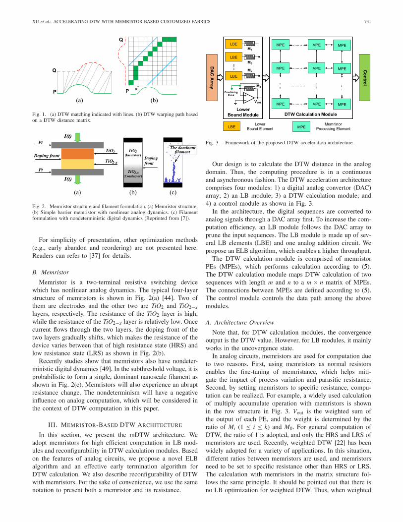
Fig. 1. (a) DTW matching indicated with lines. (b) DTW warping path basedon a DTW distance matrix.
(a) (b) (c)
Fig. 2. Memristor structure and filament formulation. (a) Memristor structure.(b) Simple barrier memristor with nonlinear analog dynamics. (c) Filamentformulation with nondeterministic digital dynamics (Reprinted from [7]).
For simplicity of presentation, other optimization methods(e.g., early abandon and reordering) are not presented here.Readers can refer to [37] for details.
B. Memristor
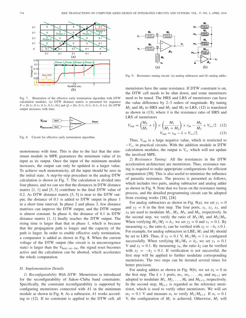
Memristor is a two-terminal resistive switching devicewhich has nonlinear analog dynamics. The typical four-layerstructure of memristors is shown in Fig. 2(a) [44]. Two ofthem are electrodes and the other two are TiO2 and TiO2−x
layers, respectively. The resistance of the TiO2 layer is high,while the resistance of the TiO2−x layer is relatively low. Oncecurrent flows through the two layers, the doping front of thetwo layers gradually shifts, which makes the resistance of thedevice varies between that of high resistance state (HRS) andlow resistance state (LRS) as shown in Fig. 2(b).
Recently studies show that memristors also have nondeter-ministic digital dynamics [49]. In the subthreshold voltage, it isprobabilistic to form a single, dominant nanoscale filament asshown in Fig. 2(c). Memristors will also experience an abruptresistance change. The nondeterminism will have a negativeinfluence on analog computation, which will be considered inthe context of DTW computation in this paper.
III. MEMRISTOR-BASED DTW ARCHITECTURE
In this section, we present the mDTW architecture. Weadopt memristors for high efficient computation in LB mod-ules and reconfigurability in DTW calculation modules. Basedon the features of analog circuits, we propose a novel ELBalgorithm and an effective early termination algorithm forDTW calculation. We also describe reconfigurability of DTWwith memristors. For the sake of convenience, we use the samenotation to present both a memristor and its resistance.
Fig. 3. Framework of the proposed DTW acceleration architecture.
Our design is to calculate the DTW distance in the analogdomain. Thus, the computing procedure is in a continuousand asynchronous fashion. The DTW acceleration architecturecomprises four modules: 1) a digital analog convertor (DAC)array; 2) an LB module; 3) a DTW calculation module; and4) a control module as shown in Fig. 3.
In the architecture, the digital sequences are converted toanalog signals through a DAC array first. To increase the com-putation efficiency, an LB module follows the DAC array toprune the input sequences. The LB module is made up of sev-eral LB elements (LBE) and one analog addition circuit. Wepropose an ELB algorithm, which enables a higher throughput.
The DTW calculation module is comprised of memristorPEs (MPEs), which performs calculation according to (5).The DTW calculation module maps DTW calculation of twosequences with length m and n to a m × n matrix of MPEs.The connections between MPEs are defined according to (5).The control module controls the data path among the abovemodules.
A. Architecture Overview
Note that, for DTW calculation modules, the convergenceoutput is the DTW value. However, for LB modules, it mainlyworks in the uncovergence state.
In analog circuits, memristors are used for computation dueto two reasons. First, using memristors as normal resistorsenables the fine-tuning of memristance, which helps miti-gate the impact of process variation and parasitic resistance.Second, by setting memristors to specific resistance, compu-tation can be realized. For example, a widely used calculationof multiply accumulate operation with memristors is shownin the row structure in Fig. 3. Vout is the weighted sum ofthe output of each PE, and the weight is determined by theratio of Mi (1 ≤ i ≤ k) and M0. For general computation ofDTW, the ratio of 1 is adopted, and only the HRS and LRS ofmemristors are used. Recently, weighted DTW [22] has beenwidely adopted for a variety of applications. In this situation,different ratios between memristors are used, and memristorsneed to be set to specific resistance other than HRS or LRS.The calculation with memristors in the matrix structure fol-lows the same principle. It should be pointed out that there isno LB optimization for weighted DTW. Thus, when weighted

732 IEEE TRANSACTIONS ON COMPUTER-AIDED DESIGN OF INTEGRATED CIRCUITS AND SYSTEMS, VOL. 37, NO. 4, APRIL 2018
Fig. 4. Circuit structure (the resistance of memristors change accordingconfigurations) of LBE.
DTW is adopted, LB computation is not involved. Within ana-log circuits, the computation is conducted in a parallel manner.We discover that with identical circuit structures for inputs inthe LB module, the relations of outputs in converage state andunconverage state are the same, which could be used for fur-ther optimization. The details of implementations are discussedin following sections.
Note that the nonlinear behavior of the memristor modelis only used for resistance tuning. It is strictly avoidedfor accurate computation during normal operation [31],which is achieved with a low load voltage as discussed inSection IV-A. Thus, the polarity of memristors will not affectthe performance, which is not indicated in all the figures inthis paper.
B. Memristor-Based Lower Bound Module
1) Hardware Implementation: LBE realizes the functionof (8) as shown in Fig. 4. By combining multiple LBEs,memristors, and one amplifier, the function in (9) is achieved.
LBE includes two modules: 1) a selecting module and2) a computing module. The computing module has two ana-log subtractors, which are responsible for Qi − Pi,upper andPi,lower−Qi, respectively. The selecting module with compara-tors and transmission gates determines which result should beconnected to the output port. With the obtained Di from LBE,Vout in LB modules as shown in Fig. 3 can be formulated asfollows:
Vout = M0 ×∑ Di
Mi=
∑ M0
Mi× Di. (10)
Combining (9) and (10), it can be noted that by tuningmemristors to Mi = M0, Vout is exactly the expected output,LB(P, Q). Note that the tuning processing is presented onlyonce for specific applications.
2) Algorithm Optimization: We propose an ELB algorithmto accelerate LB computation. In the LB module, each inputhas an equal position to each other, and the circuit structure
Fig. 5. Illustration of ELB algorithm. The relationship of the three LBoutputs are the same in unconvergence and convergence states.
Algorithm 1 ELB AlgorithmRequire: Test, Template[n];Ensure: The minimum DTW distance;
1: dtwbsf← INF;2: elbnu← INF;elbbsf← INF;3: lbnu← INF;lbbsf← INF;4: for i = 1→ n do5: elbi←FuncEarlyLowerBound(Test, Template[i]);6: if elbi ← elbnu then7: lbi←FuncLowerBound(Test, Template[i]);8: if lbi ← dtwbsf then9: dtwi←FuncDTW(Test, Template[i]);
10: if dtwi ← dtwbsf then11: if lbbsf ← dtwi then12: elbnu←elbbsf ; lbnu←lbbsf ;13: end if14: dtwbsf←dtwi; lbbsf←lbi; elbbsf←elbi;15: end if16: else17: elbnu←elbbsf ; lbnu←lbbsf ;18: end if19: end if20: end for21: Return dtwbsf ;
for each input is identical. With this character, early decisionin LB modules can be achieved, which means LB modulescan process sequences with a shorter time rather than the con-vergence time. The detail is illustrated in Fig. 5. It can benoted that the relation of |V(lb1)|, |V(lb2)|, and |V(lb3)| in theunconvergence state and the convergence state are the same.
Based on this phenomenon, we propose a novel ELB algo-rithm shown in Algorithm 1. The general LB algorithm hasto wait for the convergence state of the circuit to obtain LB,lb, for pruning. However, ELB algorithm prunes sequenceswith the ELB, elb, when the circuit is in unconvergence state.Thus, high throughput processing can be achieved. The sam-pling point is defined as Early Point, and the interval betweenthe rising edge of the input and Early Point is defined as EarlyInterval. ELB algorithm maintains the nearest upper lbnu to thebest DTW, dtwbsf, and its elbnu is also stored.
We provide an example to explain how ELB algorithmworks. As shown in Fig. 5, Early Point is set to 1.5 ns, andEarly Interval is 0.5 ns. In the following discussion, all vari-ables are the absolute values of their corresponding voltages

XU et al.: ACCELERATING DTW WITH MEMRISTOR-BASED CUSTOMIZED FABRICS 733
Fig. 6. Circuit structure of MPE (the resistance of memristors changeaccording configurations).
for simplification. The first sequence, S1, is calculated, and itsLB lb1 at 1.5 ns, elb1, is also obtained. Thus, dtwbsf = dtw1,elbbsf = elb1, and lbbsf = lb1. By calculating the LB ofsequence, S2, it is pruned as its LB, lb2, is larger than dtwbsf.The absolute value of the LB lb2 at 1.5 ns, elb2, can beobtained. Then, elbnu = elb2 and lbnu = lb2. When calcu-lating the LB of sequence, S3, waiting for the convergencestate is not needed. We can just obtain elb3, and comparisonis made between elb3 and elbnu. As elb3 is larger than lbnu,it can be predicted that lb3 is larger than lb2 in the conver-gence state. Thus, the LB and DTW calculation of S3 canbe aborted. Otherwise, elb3 will be bypassed and DTW com-putation is needed. The nearest upper lbnu, can be updatedand it can be rather tight, which can prune a large number ofsequences.
C. DTW Calculation Module
1) Hardware Implementation: The DTW calculation mod-ule is shown in Fig. 6, which includes three modules:1) absolution module; 2) minimum module; and 3) additionmodule. The absolution module calculates the absolute valueof (Pi − Qj). Two analog subtractors are used for calculating(Pi−Qj) and (Qj−Pi), respectively. Two diodes are to outputthe larger value of the two values. Thus, the output value isthe positive value, which is the absolute value of (Pi − Qj).For conditions of Pi = Qj, the output is also correct.
The minimum module obtains the minimum value ofW(i, j − 1), W(i − 1, j), and W(i − 1, j − 1). As diodes areperfect for maximum value calculation, we transform the min-imum calculation to a maximum problem as shown in (11),where Vcc is the supply voltage. In step 1 of (11), the min-imum problem is converted to a maximum problem, whichcan be easily calculated with diodes. However, there is a seri-ous problem in the designs according to step 1. With diodes,the input current for the analog subtracter is fixed to posi-tive, which means there is no negative current. As a result,the diode works in the cutoff region when the input is lessthan Vcc/4, and there is no current for the input. Thus, themaximum value of the output is Vcc/4, which is sufficient forDTW calculation. Step 2 is introduced to tackle the problem.The input and Vcc/2 switches their roles and are connected asshown in Fig. 6. Then the output is the minimum value with anegative sign, which can be easily solved by converting addi-tion to subtraction. Weight factor wi,j supports weighted DTW,which can be achieved by configure memristors M1 and M2to M1/M2 = (2−wi,j)/wi,j. Other memristors are all with thesame resistance.
W(i, j) = wi,j∣∣Pi − Qj
∣∣+min(Wi,j−1, Wi−1,j, Wi−1,j−1
)
= wi,j∣∣Pi − Qj
∣∣+ {Vcc/2−max
(Vcc −Wi,j−1
× Vcc/2−Wi,j−1, Vcc/2−Wi,j−1)}
Step 1
= wi,j∣∣Pi − Qj
∣∣− {max
(Vcc/2−Wi,j−1, Vcc/2
− Wi,j−1, Vcc/2−Wi,j−1)− Vcc/2
}Step 2.
(11)
We take a more detailed discussion of the minimum module.With the feature of diodes, the output voltage of each diodein the minimum module must be above zero. Therefore, ifinputs W(i, j), W(i − 1, j), and W(i, j − 1) are all larger thanVcc/2, the output voltages of A1, A2, and A3 are all belowzero, and the output voltages of the three diodes will be zero.This will result in a smaller output voltage of the MPE than itshould be, which may cause a large relative error in the DTWcomputation. However, we can make a reasonable assumptionhere that MPEs with inputs W(i, j), W(i−1, j), and W(i, j−1)
all larger than Vcc/2 have no impact on the results from theperspective of tasks. For tasks such as similarity search andclassification, only low distances between templates and thetest are considered, which has influence on the task results. Ifthis MPE is not in the shortest path, it has no impact in theresults and the assumption is verified. Otherwise, the outputvoltage of the DTW computation must be larger than Vcc/2.With proper voltage quantization, Vcc/2 corresponds to a verylarge DTW value, and the actual DTW value is even larger.Thus, the template with this DTW value has no impact on thetask results and the assumption is also valid.
2) Algorithm Optimization: In this section, we proposean effective early termination algorithm to accelerate DTWcomputation. Early abandon is a very effective method thatcan further prune the DTW computations [37]. In this paper,we propose an effective early termination algorithm, whichcan achieve early abandon in DTW computation in the ana-log domain. We observe that the voltage of DTW output is
734 IEEE TRANSACTIONS ON COMPUTER-AIDED DESIGN OF INTEGRATED CIRCUITS AND SYSTEMS, VOL. 37, NO. 4, APRIL 2018
(a)
(b)
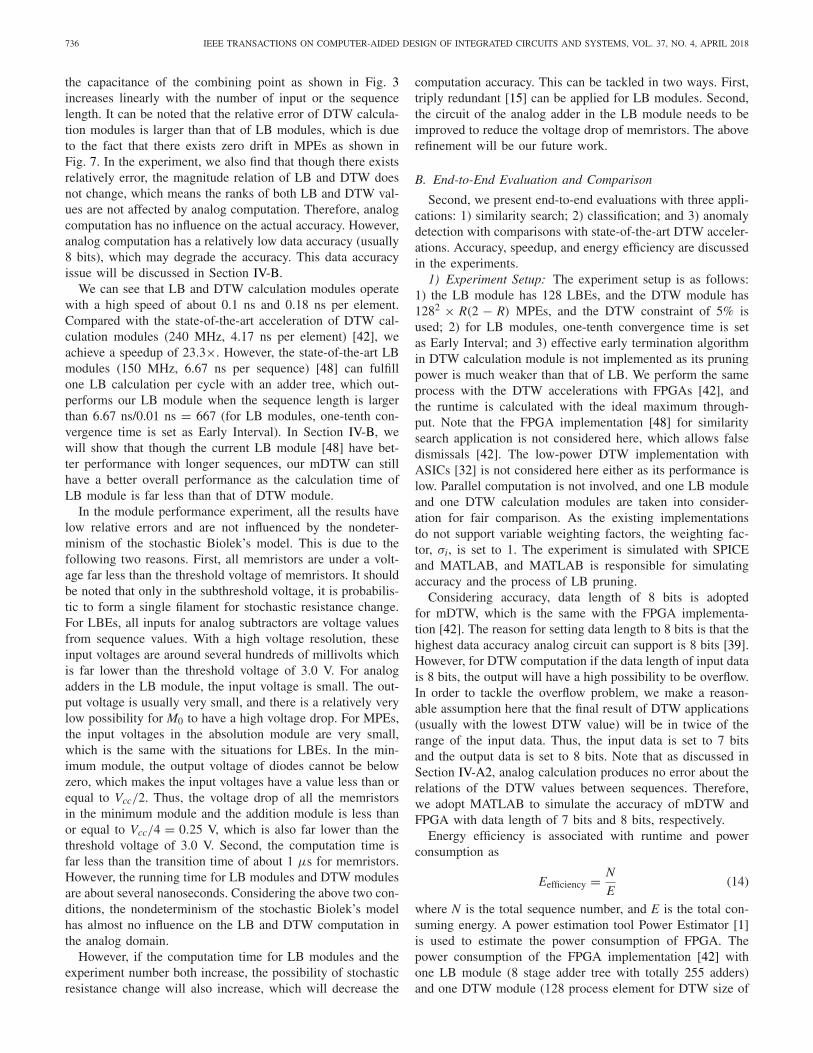
Fig. 7. Illustration of the effective early termination algorithm with DTWcalculation modules. (a) DTW distance matrix is presented for sequenceP = [0.1v, 0.1v, 0.1v, 0.1v, 0v] and Q = [0v, 0.1v, 0.1v, 0.1v, 0.1v]. (b) DTWoutput increases with time.
Fig. 8. Circuit for effective early termination algorithm.
monotonous with time. This is due to the fact that the min-imum module in MPE guarantees the minimum value of itsinput as its output. Once the input of the minimum moduleincreases, the output can only be updated to a larger value.To achieve such monotonicity, all the input should be zero inthe initial state. A step-by-step procedure in the analog DTWcalculation is shown in Fig. 7. The calculation is divided intofour phases, and we can see that the distances in DTW distancematrix [1, 1] and [5, 5] contribute to the final DTW value of0.2. As DTW distance matrix [5, 5] is near to the DTW out-put, the distance of 0.1 is added to DTW output in phase 1in a short time interval. In phase 2 and phase 3, few distancematrixes can improve the DTW output, and the DTW outputis almost constant. In phase 4, the distance of 0.1 in DTWdistance matrix [1, 1] finally reaches the DTW output. Therising time is larger than that in phase 1, which is becausethat the propagation path is longer and the capacity of thepath is larger. In order to enable effective early termination,a comparator is added as shown in Fig. 8. When the currentvoltage of the DTW output (the circuit is in unconvergencestate) is larger than the Vbest−so−far, the signal reset becomesactive and the calculation can be aborted, which acceleratesthe whole computation.
D. Implementation Details
1) Reconfigurability With DTW: Memristors is introducedfor the reconfigurability of Sakoe–Chiba band constraints.Specifically, the constraint reconfigurability is supported byconfiguring memristors connected with A1 in the minimummodule as shown in Fig. 6. As a subtractor, A1 works accord-ing to (12). If no constraint is applied to the DTW cell, all
(a) (b)
Fig. 9. Resistance tuning circuit: (a) analog subtractor and (b) analog adder.
memristors have the same resistance. If DTW constraint is on,the DTW cell needs to be shut down, and some memristorsneed to be tuned. The HRS and LRS of memristors can havethe value difference by 2–3 orders of magnitude. By tuningM2 and M4 to HRS and M1 and M3 to LRS, (12) is translatedas shown in (13), where δ is the resistance ratio of HRS andLRS of memristors
Vout =(
M4
M3+ 1
)×
(M1
M1 +M2
)× vin − M4
M3× Vcc/2 (12)
Vout = vin − δ × Vcc/2. (13)
Thus, Vout is a large negative value, which is restricted to−Vcc in practical circuits. With the addition module in DTWcalculation modules, the output is Vcc which will not updatethe involved MPE.
2) Resistance Tuning: All the resistances in the DTWacceleration architecture are memristors. Thus, resistance tun-ing is required to make appropriate configurations for efficientcomputation [30]. This is also useful to minimize the influenceof parasitic resistance. The process is presented as follows,which includes two parts, analog subtractor and analog adderas shown in Fig. 9. Note that we focus on the resistance tuningprocess, and the detailed programming circuit can be adoptedfrom existing works [18], [24].
For analog subtractors as shown in Fig. 9(a), we set y1 = 0and y2 = 0 in the first step. The four ports, x1, x2, x3, andx4 are used to modulate M1, M2, M3, and M4, respectively. Inthe second step, we verify the ratio of M1/M2 and M3/M4.When verifying M1/M2 = k1, we set y2 = 0 and x1 = 0.1. Bymeasuring x2, the ratio k1 can be verified with x2 = −k1×0.1.For example, for analog subtractors in LBE, M1 and M2 shouldbe set to LRS. Thus, if x2 = 0.1 V, M1/M2 = 1 is configuredsuccessfully. When verifying M3/M4 = k2, we set y1 = 0.1V and x3 = 0.1. By measuring x4, the ratio k2 can be verifiedwith x2 = −k2 × 0.1. If verification is not successful, thefirst step will be applied to further modulate correspondingmemristors. The two steps can be iterated several times forbetter precision.
For analog adders as shown in Fig. 9(b), we set n2 = 0 inthe first step. The k + 1 ports, m1, m2, . . . , mk and mk+1 areadopted to modulate M1, M2, . . . , Mk and Mk+1, respectively.In the second step, Mk+1 is regarded as the reference mem-ristor, which is used to verify other memristors. We will setm1 = 0.1 V and measure n1 to verify M1/Mk+1. If n1 = 0.1V, the configuration of M1 is achieved. Otherwise, M1 will

XU et al.: ACCELERATING DTW WITH MEMRISTOR-BASED CUSTOMIZED FABRICS 735
TABLE IDTW ARCHITECTURE SETUP
be modulated according to the offset to the configuration.The process of modulation and verification can be iteratedfor higher precision. The above tuning process for M1 will beapplied to other memristors.
For situations where the threshold voltage of memristors islarger than the supply voltage under some technology node,dual power can be adopted to avoid the possible damage totransistors by the large voltage for resistance tuning. With dualpower, one supply voltage is for normal operation and anotherone is for memristor tuning. If memristor tuning is needed, thenormal supply voltage is off and the tuning supply voltage ison. Each memristor need to be programmed individually, andthe two ports of it need to be connected to the programmingcircuit.
3) Impact of Process Variation: Considering process vari-ation, the actual resistance of memristors have a tolerance of±20% to ±30%, which will degrade the solution quality. Twosteps are adopted to reduce the impact of process variation.First, we can discover that the solution quality is only the ratioof memristors. Thus, tolerance control technique [16] can beused to restrict the tolerance between two memristors lowerthan 1%. Second, post-fabrication resistance tuning can furtherreduce the negative effects of process variation.
IV. PERFORMANCE SIMULATION
In this section, we perform module and end-to-end eval-uations of the proposed mDTW architecture with respectto accuracy, throughput, and energy efficiency. The threewidely used applications, similarity search, classification, andanomaly detection are employed in the end-to-end evalua-tion. Specifically, the performance of the mDTW architectureobtained via simulations with SPICE [35] and MATLAB [21]is compared with existing works on GPUs and FPGAs.
A. Module Evaluation
1) Experimental Setup: We implement the proposed designin SPICE [35] with the 32 nm technology node, and the simu-lation setup is presented in Table I. For the sake of generality,the parameters of op-amps and diodes are set to typical valuesaccording to [8] and [31]. Particularly, a parasitic capacitanceof 20fF is added to each circuit net to model the effect ofparasitic capacitance [31]. The stochastic Biolek’s model [7]for memristor is adopted and the parameters of the model areshown in Table II. All the parameters of the model are adoptedfrom [7].
The parameter voltage resolution is to translate sequencevalues to voltages. We set the voltage resolution to a rela-tively large value of 125 mV. Longer sequence length need
TABLE IISTOCHASTIC BIOLEK’S MODEL PARAMETERS
Fig. 10. Convergence time and relative error of LB module.
Fig. 11. Convergence time and relative error of DTW calculation module.
smaller voltage resolution. The translation process is as fol-lows: after normalization, the sequence value 1 is translatedto 125 mV. Other values follow the same principle, e.g., 1.2and −0.5 are translated to 150 mV and −62.5 mV, respec-tively. In fact, it is still possible that the output voltage willoverflow. As discussed in Section III-C, we make a reasonableassumption that overflowed outputs have no influence on datamining tasks. For DTW configuration, warping constraint of5% is adopted.
2) Module Performance Characterization: First, we presentperformance evaluation for each module in the mDTW archi-tecture. The convergence time which indicates how fast theanalog circuit can operate is discussed. The convergence timeis defined as the interval between the rising edge of the inputand the timestamp when the DTW output is within 0.1% ofthe final value. We also analyze the relative error of the circuitsolution compared to the optimal solution.
We adopt three data sets (Beef, Symbols, and OSU Leaf)from UCR Time Series Classification Archive [23]. For eachdata set, we formalize the sequences with different lengths.Note that two sequences for computation have the same length.From each dataset, we select 21 sequences and select the firstsequence as the query, and LB and DTW computation areperformed with the query and the rest 20 sequences.
The maximum convergence time and relative error of LBmodules and DTW calculation modules are presented inFigs. 10 and 11, respectively. We can observe that the conver-gence time of both LB modules and DTW calculation modulesare almost linear to the sequence length. This is due to the factthat both modules have a linear capacitance to the input sizein the current propagation path. Specifically, for LB modules,
736 IEEE TRANSACTIONS ON COMPUTER-AIDED DESIGN OF INTEGRATED CIRCUITS AND SYSTEMS, VOL. 37, NO. 4, APRIL 2018
the capacitance of the combining point as shown in Fig. 3increases linearly with the number of input or the sequencelength. It can be noted that the relative error of DTW calcula-tion modules is larger than that of LB modules, which is dueto the fact that there exists zero drift in MPEs as shown inFig. 7. In the experiment, we also find that though there existsrelatively error, the magnitude relation of LB and DTW doesnot change, which means the ranks of both LB and DTW val-ues are not affected by analog computation. Therefore, analogcomputation has no influence on the actual accuracy. However,analog computation has a relatively low data accuracy (usually8 bits), which may degrade the accuracy. This data accuracyissue will be discussed in Section IV-B.
We can see that LB and DTW calculation modules operatewith a high speed of about 0.1 ns and 0.18 ns per element.Compared with the state-of-the-art acceleration of DTW cal-culation modules (240 MHz, 4.17 ns per element) [42], weachieve a speedup of 23.3×. However, the state-of-the-art LBmodules (150 MHz, 6.67 ns per sequence) [48] can fulfillone LB calculation per cycle with an adder tree, which out-performs our LB module when the sequence length is largerthan 6.67 ns/0.01 ns = 667 (for LB modules, one-tenth con-vergence time is set as Early Interval). In Section IV-B, wewill show that though the current LB module [48] have bet-ter performance with longer sequences, our mDTW can stillhave a better overall performance as the calculation time ofLB module is far less than that of DTW module.
In the module performance experiment, all the results havelow relative errors and are not influenced by the nondeter-minism of the stochastic Biolek’s model. This is due to thefollowing two reasons. First, all memristors are under a volt-age far less than the threshold voltage of memristors. It shouldbe noted that only in the subthreshold voltage, it is probabilis-tic to form a single filament for stochastic resistance change.For LBEs, all inputs for analog subtractors are voltage valuesfrom sequence values. With a high voltage resolution, theseinput voltages are around several hundreds of millivolts whichis far lower than the threshold voltage of 3.0 V. For analogadders in the LB module, the input voltage is small. The out-put voltage is usually very small, and there is a relatively verylow possibility for M0 to have a high voltage drop. For MPEs,the input voltages in the absolution module are very small,which is the same with the situations for LBEs. In the min-imum module, the output voltage of diodes cannot be belowzero, which makes the input voltages have a value less than orequal to Vcc/2. Thus, the voltage drop of all the memristorsin the minimum module and the addition module is less thanor equal to Vcc/4 = 0.25 V, which is also far lower than thethreshold voltage of 3.0 V. Second, the computation time isfar less than the transition time of about 1 μs for memristors.However, the running time for LB modules and DTW modulesare about several nanoseconds. Considering the above two con-ditions, the nondeterminism of the stochastic Biolek’s modelhas almost no influence on the LB and DTW computation inthe analog domain.
However, if the computation time for LB modules and theexperiment number both increase, the possibility of stochasticresistance change will also increase, which will decrease the
computation accuracy. This can be tackled in two ways. First,triply redundant [15] can be applied for LB modules. Second,the circuit of the analog adder in the LB module needs to beimproved to reduce the voltage drop of memristors. The aboverefinement will be our future work.
B. End-to-End Evaluation and Comparison
Second, we present end-to-end evaluations with three appli-cations: 1) similarity search; 2) classification; and 3) anomalydetection with comparisons with state-of-the-art DTW acceler-ations. Accuracy, speedup, and energy efficiency are discussedin the experiments.
1) Experiment Setup: The experiment setup is as follows:1) the LB module has 128 LBEs, and the DTW module has1282 × R(2 − R) MPEs, and the DTW constraint of 5% isused; 2) for LB modules, one-tenth convergence time is setas Early Interval; and 3) effective early termination algorithmin DTW calculation module is not implemented as its pruningpower is much weaker than that of LB. We perform the sameprocess with the DTW accelerations with FPGAs [42], andthe runtime is calculated with the ideal maximum through-put. Note that the FPGA implementation [48] for similaritysearch application is not considered here, which allows falsedismissals [42]. The low-power DTW implementation withASICs [32] is not considered here either as its performance islow. Parallel computation is not involved, and one LB moduleand one DTW calculation modules are taken into consider-ation for fair comparison. As the existing implementationsdo not support variable weighting factors, the weighting fac-tor, σi, is set to 1. The experiment is simulated with SPICEand MATLAB, and MATLAB is responsible for simulatingaccuracy and the process of LB pruning.
Considering accuracy, data length of 8 bits is adoptedfor mDTW, which is the same with the FPGA implementa-tion [42]. The reason for setting data length to 8 bits is that thehighest data accuracy analog circuit can support is 8 bits [39].However, for DTW computation if the data length of input datais 8 bits, the output will have a high possibility to be overflow.In order to tackle the overflow problem, we make a reason-able assumption here that the final result of DTW applications(usually with the lowest DTW value) will be in twice of therange of the input data. Thus, the input data is set to 7 bitsand the output data is set to 8 bits. Note that as discussed inSection IV-A2, analog calculation produces no error about therelations of the DTW values between sequences. Therefore,we adopt MATLAB to simulate the accuracy of mDTW andFPGA with data length of 7 bits and 8 bits, respectively.
Energy efficiency is associated with runtime and powerconsumption as
Eefficiency = N
E(14)
where N is the total sequence number, and E is the total con-suming energy. A power estimation tool Power Estimator [1]is used to estimate the power consumption of FPGA. Thepower consumption of the FPGA implementation [42] withone LB module (8 stage adder tree with totally 255 adders)and one DTW module (128 process element for DTW size of
XU et al.: ACCELERATING DTW WITH MEMRISTOR-BASED CUSTOMIZED FABRICS 737
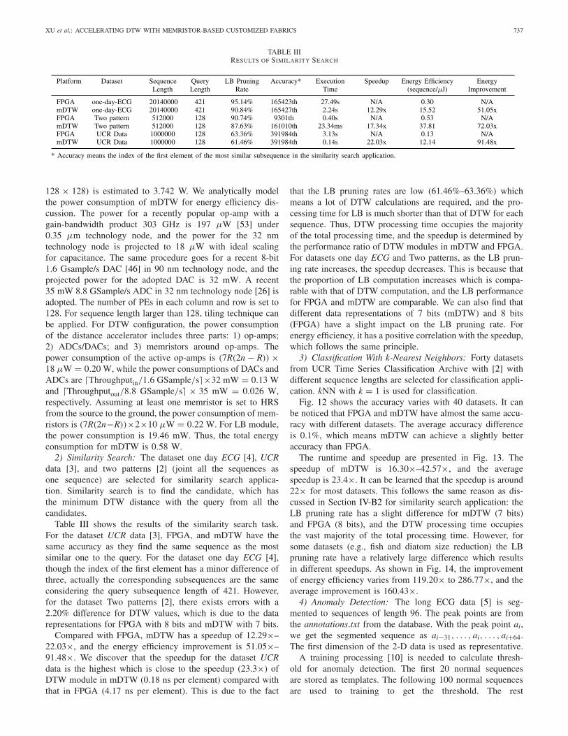
TABLE IIIRESULTS OF SIMILARITY SEARCH
128 × 128) is estimated to 3.742 W. We analytically modelthe power consumption of mDTW for energy efficiency dis-cussion. The power for a recently popular op-amp with again-bandwidth product 303 GHz is 197 μW [53] under0.35 μm technology node, and the power for the 32 nmtechnology node is projected to 18 μW with ideal scalingfor capacitance. The same procedure goes for a recent 8-bit1.6 Gsample/s DAC [46] in 90 nm technology node, and theprojected power for the adopted DAC is 32 mW. A recent35 mW 8.8 GSample/s ADC in 32 nm technology node [26] isadopted. The number of PEs in each column and row is set to128. For sequence length larger than 128, tiling technique canbe applied. For DTW configuration, the power consumptionof the distance accelerator includes three parts: 1) op-amps;2) ADCs/DACs; and 3) memristors around op-amps. Thepower consumption of the active op-amps is (7R(2n − R))×18 μW = 0.20 W, while the power consumptions of DACs andADCs are �Throughputin/1.6 GSample/s×32 mW = 0.13 Wand �Throughputout/8.8 GSample/s × 35 mW = 0.026 W,respectively. Assuming at least one memristor is set to HRSfrom the source to the ground, the power consumption of mem-ristors is (7R(2n−R))×2×10 μW = 0.22 W. For LB module,the power consumption is 19.46 mW. Thus, the total energyconsumption for mDTW is 0.58 W.
2) Similarity Search: The dataset one day ECG [4], UCRdata [3], and two patterns [2] (joint all the sequences asone sequence) are selected for similarity search applica-tion. Similarity search is to find the candidate, which hasthe minimum DTW distance with the query from all thecandidates.
Table III shows the results of the similarity search task.For the dataset UCR data [3], FPGA, and mDTW have thesame accuracy as they find the same sequence as the mostsimilar one to the query. For the dataset one day ECG [4],though the index of the first element has a minor difference ofthree, actually the corresponding subsequences are the sameconsidering the query subsequence length of 421. However,for the dataset Two patterns [2], there exists errors with a2.20% difference for DTW values, which is due to the datarepresentations for FPGA with 8 bits and mDTW with 7 bits.
Compared with FPGA, mDTW has a speedup of 12.29×–22.03×, and the energy efficiency improvement is 51.05×–91.48×. We discover that the speedup for the dataset UCRdata is the highest which is close to the speedup (23.3×) ofDTW module in mDTW (0.18 ns per element) compared withthat in FPGA (4.17 ns per element). This is due to the fact
that the LB pruning rates are low (61.46%–63.36%) whichmeans a lot of DTW calculations are required, and the pro-cessing time for LB is much shorter than that of DTW for eachsequence. Thus, DTW processing time occupies the majorityof the total processing time, and the speedup is determined bythe performance ratio of DTW modules in mDTW and FPGA.For datasets one day ECG and Two patterns, as the LB prun-ing rate increases, the speedup decreases. This is because thatthe proportion of LB computation increases which is compa-rable with that of DTW computation, and the LB performancefor FPGA and mDTW are comparable. We can also find thatdifferent data representations of 7 bits (mDTW) and 8 bits(FPGA) have a slight impact on the LB pruning rate. Forenergy efficiency, it has a positive correlation with the speedup,which follows the same principle.
3) Classification With k-Nearest Neighbors: Forty datasetsfrom UCR Time Series Classification Archive with [2] withdifferent sequence lengths are selected for classification appli-cation. kNN with k = 1 is used for classification.
Fig. 12 shows the accuracy varies with 40 datasets. It canbe noticed that FPGA and mDTW have almost the same accu-racy with different datasets. The average accuracy differenceis 0.1%, which means mDTW can achieve a slightly betteraccuracy than FPGA.
The runtime and speedup are presented in Fig. 13. Thespeedup of mDTW is 16.30×–42.57×, and the averagespeedup is 23.4×. It can be learned that the speedup is around22× for most datasets. This follows the same reason as dis-cussed in Section IV-B2 for similarity search application: theLB pruning rate has a slight difference for mDTW (7 bits)and FPGA (8 bits), and the DTW processing time occupiesthe vast majority of the total processing time. However, forsome datasets (e.g., fish and diatom size reduction) the LBpruning rate have a relatively large difference which resultsin different speedups. As shown in Fig. 14, the improvementof energy efficiency varies from 119.20× to 286.77×, and theaverage improvement is 160.43×.
4) Anomaly Detection: The long ECG data [5] is seg-mented to sequences of length 96. The peak points are fromthe annotations.txt from the database. With the peak point ai,we get the segmented sequence as ai−31, . . . , ai, . . . , ai+64.The first dimension of the 2-D data is used as representative.
A training processing [10] is needed to calculate thresh-old for anomaly detection. The first 20 normal sequencesare stored as templates. The following 100 normal sequencesare used to training to get the threshold. The rest

738 IEEE TRANSACTIONS ON COMPUTER-AIDED DESIGN OF INTEGRATED CIRCUITS AND SYSTEMS, VOL. 37, NO. 4, APRIL 2018
Fig. 12. Accuracy of classification application with kNN. The correspondence of dataset and the x-axis is as follows: (1, 50Words), (2, Adiac), (3, Beef),(4, CBF), (5, Coffee), (6, ECG200), (7, Face All), (8, Face Four), (9, fish), (10, Gun_Point), (11, Lighting2), (12, Lighting7), (13, Olive Oil), (14, OSULeaf), (15, Swedish Leaf), (16, synthetic_control), (17, Trace), (18, Two_Patterns), (19, wafer), (20, yoga), (21, Chlorine_Concentration), (22, AdCinC ECGtorsoiac), (23, Cricket X), (24, Cricket Y), (25, Cricket Z), (26, Diatom Size Reduction), (27, ECG Five Days), (28, Faces UCR), (29, Haptics), (30, InlineSkate), (31, Italy Power Demand), (32, MALLAT), (33, Medical Images), (34, Mote Strain), (35, Sony AIBO Robot Surface), (36, Sony AIBO Robot SurfaceII), (37, Star Light Curves), (38, Symbols), (39, Two Lead ECG), (40, uWave Gesture Library X), where X is the x-axis and A is the name of dataset in theformat (X, A).
Fig. 13. Runtime and speedup of classification application with kNN. See the caption of Fig. 12 for the detail information of the x-axis dataset.
Fig. 14. Energy efficiency and improvement of classification application with kNN. See the caption of Fig. 12 for the detail information of the x-axis dataset.
of the ECG sequences are treated as the data to bedetected.
For compact demonstration, accuracy and precision in theconfusion matrix are selected to discuss the performance. Asshown in Fig. 15, the accuracy and precision of FPGA andmDTW are almost the same for different datasets.
Fig. 16 shows the runtime comparison of FPGA and mDTW.The speedup varies from 20.95× to 23.64× with differ-ent dataset IDs, which follows the same principle discussedin Sections IV-B2 and IV-B3. As shown in Fig. 17, theenergy efficiency improvements of mDTW over FPGA is143.74×–152.49×.
V. RELATED WORK
There is a large body of work exploring the noveltyof memristor in new emerging fields beyond the straight-forward memory application. One of the most impor-tant applications is neuromorphic systems [17], [28], [29],
Fig. 15. Accuracy and precision of anomaly detection application.
which adopts crossbar structure for efficient computation.Another important memristor application is analog and dig-ital circuits. Logic/arithmetic operation [9] and programmablemodules (e.g., filters [33], Chaos circuit [34], and memristor-based arithmetic-logic unit [47]) benefit from the featureof programmability. Memristor has also been applied toefficient architectures for area and energy optimization,e.g., FPGA+memristor [11] and FPAA+memristor [27].

XU et al.: ACCELERATING DTW WITH MEMRISTOR-BASED CUSTOMIZED FABRICS 739
Fig. 16. Runtime of anomaly detection application.
Fig. 17. Energy efficiency and improvement of anomaly detection applica-tion.
Recently, memristor has been adopted for algorithm opti-mization in analog domain. Liu and Zhang [31] implementedan analog substrate with memristors for max flow problem andachieves a speedup of 150× to 1500×. Memristor has alsobeen applied to maze [36], shortest path algorithm [50], andbin packing algorithm [43]. The features in analog domaingive a new sight for the improvement of performance. Thispaper is another exploring work of memristors in the matchingalgorithm application.
VI. CONCLUSION
In this paper, we propose a high-throughput and energyefficient mDTW architecture for time series mining on datacenters. We performed memristor-based analog circuit designsfor LB modules and DTW calculation modules. Based onthe feature of analog circuits, we developed a novel ELBalgorithm and an effective early termination algorithm forDTW computation acceleration. We also achieved recon-figurability in DTW calculation modules with memristors.Comprehensive experiments are presented with public avail-able datasets. Module evaluation and end-to-end evaluationincluding similarity search, classification, and anomaly detec-tion applications are presented. Experimental results showthat the proposed mDTW can achieve a speedup and anenergy efficiency improvement of 12×–43× and 51×–287×,respectively.
REFERENCES
[1] Xilinx Power Estimator (XPE). Accessed onDec. 6, 2016. [Online]. Available: https://www.xilinx.com/products/technology/power/xpe.html
[2] The UCR Time Series Classification Archive. Accessed onOct. 15, 2016. [Online]. Available: http://www.cs.ucr.edu/∼eamonn/time_series_data/
[3] The UCR Suite Trillion Dataset. Accessed on Oct. 15, 2016. [Online].Available: http://www.cs.ucr.edu/∼eamonn/trillion.zip
[4] The UCR Suite. Accessed on Oct. 15, 2016. [Online]. Available: http://www.cs.ucr.edu/∼eamonn/ucrsuite.html
[5] The MIT-BIH Long Term Database. Accessed onOct. 5, 2016. [Online]. Available: http://www.physionet.org/physiobank/database/ltdb/
[6] A. Adshead. (2014). Data Set to Grow 10-Fold by 2020As Internet of Things Takes Off. [Online]. Available:http://www.computerweekly.com
[7] M. Al-Shedivat, R. Naous, G. Cauwenberghs, and K. N. Salama,“Memristors empower spiking neurons with stochasticity,” IEEE J.Emerg. Sel. Topics Circuits Syst., vol. 5, no. 2, pp. 242–253, Jun. 2015.
[8] D. Biolek, M. Di Ventra, and Y. V. Pershin, “Reliable SPICEsimulations of memristors, memcapacitors and meminductors,”Radioengineering, vol. 22, no. 4, p. 945, 2013.
[9] J. Borghetti et al., “A hybrid nanomemristor/transistor logic circuitcapable of self-programming,” Proc. Nat. Acad. Sci. USA, vol. 106,no. 6, pp. 1699–1703, 2009.
[10] I. Boulnemour, B. Boucheham, and S. Benloucif, “Improved dynamictime warping for abnormality detection in ECG time series,” inProc. Int. Conf. Bioinformat. Biomed. Eng., Granada, Spain, 2016,pp. 242–253.
[11] J. Cong and B. Xiao, “mrFPGA: A novel FPGA architecture withmemristor-based reconfiguration,” in Proc. NANOARCH, San Diego,CA, USA, 2011, pp. 1–8.
[12] G. Cormode, “Fundamentals of analyzing and mining data streams,”in Proc. Tutorial Workshop Data Stream Anal., Caserta, Italy,2007, pp. 1–5.
[13] H. Ding, G. Trajcevski, P. Scheuermann, X. Wang, and E. Keogh,“Querying and mining of time series data: Experimental comparisonof representations and distance measures,” Proc. VLDB Endowment,vol. 1, no. 2, pp. 1542–1552, 2008.
[14] A. W.-C. Fu, E. Keogh, L. Y. H. Lau, C. A. Ratanamahatana, andR. C.-W. Wong, “Scaling and time warping in time series querying,”VLDB J., vol. 17, no. 4, pp. 899–921, 2008.
[15] R. S. Glaser et al., “Process control interface system having triplyredundant remote field units,” U.S. Patent 5 428 769, Jun. 27, 1995.
[16] R. A. Hastings, The Art of Analog Layout. Upper Saddle River, NJ,USA: Prentice-Hall, 2006.
[17] M. Hu, H. Li, Q. Wu, and G. S. Rose, “Hardware realization ofBSB recall function using memristor crossbar arrays,” in Proc. DAC,San Francisco, CA, USA, 2012, pp. 498–503.
[18] M. Hu et al., “Dot-product engine for neuromorphic computing:Programming 1T1M crossbar to accelerate matrix-vector multiplica-tion,” in Proc. 53rd ACM/EDAC/IEEE Design Autom. Conf. (DAC),Austin, TX, USA, 2016, pp. 1–6.
[19] C. Hundt, B. Schmidt, and E. Schomer, “CUDA-accelerated align-ment of subsequences in streamed time series data,” in Proc. ICPP,Minneapolis, MN, USA, 2014, pp. 10–19.
[20] Gartner Says the Internet of Things Will Transform the Data Center,G. Inc., Toronto, ON, Canada, 2014.
[21] (2017). M. Inc. [Online]. Available: https://www.mathworks.com/[22] Y.-S. Jeong, M. K. Jeong, and O. A. Omitaomu, “Weighted dynamic
time warping for time series classification,” Pattern Recognit., vol. 44,no. 9, pp. 2231–2240, 2011.
[23] E. Keogh and T. Folias, The UCR Time Series Data Mining Archive,Univ. California, Riverside, CA, USA, 2002. [Online]. Available:http://www.cs.ucr.edu/eamonn/TSDMA/index.html
[24] S. Kim et al., “Experimental demonstration of a second-order mem-ristor and its ability to biorealistically implement synaptic plasticity,”Nano Lett., vol. 15, no. 3, pp. 2203–2211, 2015.
[25] S.-W. Kim, S. Park, and W. W. Chu, “An index-based approach forsimilarity search supporting time warping in large sequence databases,”in Proc. ICDE, Heidelberg, Germany, 2001, pp. 607–614.
[26] L. Kull et al., “A 35mw8 b 8.8 GS/S SAR ADC with low-power capac-itive reference buffers in 32nm digital SOI CMOS,” in Proc. VLSI,Kyoto, Japan, 2013, pp. C260–C261.
[27] M. Laiho et al., “Analog signal processing on a FPAA/memristorhybrid circuit,” in Proc. ISCAS, Melbourne, VIC, Australia, 2014,pp. 2265–2268.
[28] B. Li et al., “Memristor-based approximated computation,” in Proc.ISLPED, Beijing, China, 2013, pp. 242–247.
[29] B. Li, Y. Wang, Y. Wang, Y. Chen, and H. Yang, “Trainingitself: Mixed-signal training acceleration for memristor-based neuralnetwork,” in Proc. ASP-DAC, Singapore, 2014, pp. 361–366.
[30] B. Liu et al., “Digital-assisted noise-eliminating training for memristorcrossbar-based analog neuromorphic computing engine,” in Proc. DAC,Austin, TX, USA, 2013, pp. 1–6.

740 IEEE TRANSACTIONS ON COMPUTER-AIDED DESIGN OF INTEGRATED CIRCUITS AND SYSTEMS, VOL. 37, NO. 4, APRIL 2018
[31] G. Liu and Z. Zhang, “A reconfigurable analog substrate for highlyefficient maximum flow computation,” in Proc. DAC, San Francisco,CA, USA, 2015, pp. 1–6.
[32] R. Lotfian and R. Jafari, “An ultra-low power hardware acceleratorarchitecture for wearable computers using dynamic time warping,” inProc. DATE, Grenoble, France, 2013, pp. 913–916.
[33] F. Merrikh-Bayat and S. Bagheri-Shouraki, “Mixed analog-digitalcrossbar-based hardware implementation of sign–sign LMS adaptivefilter,” Analog Integr. Circuits Signal Process., vol. 66, no. 1, pp. 41–48,2011.
[34] B. Muthuswamy, “Implementing memristor based chaotic circuits,” Int.J. Bifurcation Chaos, vol. 20, no. 5, pp. 1335–1350, 2010.
[35] L. W. Nagel and D. O. Pederson, “SPICE: Simulation program withintegrated circuit emphasis,” Electron. Res. Lab., College Eng., Univ.California at Berkeley, Berkeley, CA, USA, Tech. Rep. UCB/ERLM382, 1973.
[36] Y. V. Pershin and M. Di Ventra, “Solving mazes with memristors:A massively parallel approach,” Phys. Rev. E, Stat. Phys. PlasmasFluids Relat. Interdiscip. Top., vol. 84, no. 4, 2011, Art. no. 046703.
[37] T. Rakthanmanon et al., “Searching and mining trillions of timeseries subsequences under dynamic time warping,” in Proc. 18th ACMSIGKDD Int. Conf. Knowl. Disc. Data Min., Beijing, China, 2012,pp. 262–270.
[38] T. M. Rath and R. Manmatha, “Word image matching using dynamictime warping,” in Proc. CVPR, vol. 2. Madison, WI, USA, 2003,pp. II-521–II-527.
[39] A. Rodríguez-Vázquez et al., “ACE16k: The third generationof mixed-signal SIMD-CNN ACE chips toward VSoCs,” IEEETrans. Circuits Syst. I, Reg. Papers, vol. 51, no. 5, pp. 851–863,May 2004.
[40] H. Sakoe and S. Chiba, “Dynamic programming algorithm optimizationfor spoken word recognition,” IEEE Trans. Acoust., Speech, SignalProcess., vol. ASSP-26, no. 1, pp. 43–49, Feb. 1978.
[41] Y. Sakurai, C. Faloutsos, and M. Yamamuro, “Stream monitoring underthe time warping distance,” in Proc. ICDE, Istanbul, Turkey, 2007,pp. 1046–1055.
[42] D. Sart, A. Mueen, W. Najjar, E. Keogh, and V. Niennattrakul,“Accelerating dynamic time warping subsequence search with GPUsand FPGAs,” in Proc. ICDM, Sydney, NSW, Australia, 2010,pp. 1001–1006.
[43] D. Stathis, I. Vourkas, and G. C. Sirakoulis, “Solving AI problemswith memristors: A case study for optimal ‘bin packing,”’ in Proc.PCI, Athens, Greece, 2014, pp. 1–6.
[44] D. B. Strukov, G. S. Snider, D. R. Stewart, and S. Williams, “Themissing memristor found,” Nature, vol. 453, no. 7191, pp. 80–83,2008.
[45] J. Tarango, E. Keogh, and P. Brisk, “Instruction set extensions fordynamic time warping,” in Proc. 9th IEEE/ACM/IFIP Int. Conf.Hardw./Softw. Codesign Syst. Syn., Montreal, QC, Canada, 2013,pp. 1–10.
[46] W.-H. Tseng, J.-T. Wu, and Y.-C. Chu, “A CMOS 8-bit 1.6-GS/s DACwith digital random return-to-zero,” IEEE Trans. Circuits Syst. II, Exp.Briefs, vol. 58, no. 1, pp. 1–5, Jan. 2011.
[47] I. Vourkas and G. C. Sirakoulis, “High-radix arithmetic-logic unit(ALU) based on memristors,” in Memristor-Based NanoelectronicComputing Circuits and Architectures. Cham, Switzerland: Springer,2016, pp. 149–172.
[48] Z. Wang et al., “Accelerating subsequence similarity search basedon dynamic time warping distance with FPGA,” in Proc. ISFPGA,Monterey, CA, USA, 2013, pp. 53–62.
[49] Y. Yang et al., “Observation of conducting filament growth innanoscale resistive memories,” Nat. Commun., vol. 3, Mar. 2012,Art. no. 732.
[50] Z. Ye, S. H. M. Wu, and T. Prodromakis, “Computing shortest pathsin 2D and 3D memristive networks,” in Memristor Networks. Cham,Switzerland: Springer, 2014, pp. 537–552.
[51] Y. Zhang, K. Adl, and J. Glass, “Fast spoken query detection usinglower-bound dynamic time warping on graphical processing units,” inProc. IEEE Int. Conf. Acoust. Speech Signal Process. (ICASSP), Kyoto,Japan, 2012, pp. 5173–5176.
[52] H. Zhou et al., “Energy-efficient pipelined DTW architecture onhybrid embedded platforms,” in Proc. 6th Int. Green Comput.Conf. Sustain. Comput. Conf. (IGSC), Las Vegas, NV, USA, 2015,pp. 1–8.
[53] L. Zuo and S. K. Islam, “Low-voltage bulk-driven operational amplifierwith improved transconductance,” IEEE Trans. Circuits Syst. I, Reg.Papers, vol. 60, no. 8, pp. 2084–2091, Aug. 2013.
Xiaowei Xu (S’14) received the B.S. and Ph.D.degrees in electronic science and technology fromthe Huazhong University of Science and Technology,Wuhan, China, in 2011 and 2016, respectively.
He is currently a Researcher with the Schoolof Optimal and Electronic Information, HuazhongUniversity of Science and Technology. He is cur-rently a Visitor with the Department of ComputerScience, University of Notre Dame, Notre Dame,IN, USA. His current research interests includebiometrics, data mining, and embedded computing.
Feng Lin (S’11–M’15) received the B.S. degreefrom Zhejiang University, Hangzhou, China, in2006, the M.S. degree from Shanghai University,Shanghai, China, in 2009, and the Ph.D. degreefrom the Department of Electrical and ComputerEngineering, Tennessee Technological University,Cookeville, TN, USA, in 2015.
He was with Alcatel-Lucent, Boulogne-Billancourt, France, from 2009 to 2010. He iscurrently a Research Scientist with the Departmentof Computer Science and Engineering, State
University of New York at Buffalo, Buffalo, NY, USA. His current researchinterests include signal processing, embedded sensing, human–computerinterface, and their applications in wireless health and biometrics.
Aosen Wang (S’15) received the B.S. degree inelectrical engineering from the University of Scienceand Technology of China, Hefei, China, in 2011. Heis currently pursuing the Ph.D. degree in computerscience and engineering with the State Universityof New York at Buffalo (University at Buffalo),Buffalo, NY, USA.
Then he joined Vimicro, Beijing, China, asan Algorithm and Software Engineer. His currentresearch interests include low-power computer archi-tecture and energy-efficient machine learning.
Xinwei Yao (M’14) received the Ph.D. degreefrom the College of Information Engineering,Zhejiang University of Technology, Hangzhou,China, in 2013.
He is currently an Associate Professor withthe College of Computer Science and Technology,Zhejiang University of Technology. His currentresearch interests include terahertz-band commu-nication networks, electromagnetic nanonetworks,wireless ad hoc and sensor networks, wireless powertransfer, and the Internet of Things.
Dr. Yao has served on technical program committees of many IEEE/ACMconferences. He is a member of ACM.
Qing Lu received the B.E. degree in electronic andinformation engineering from the Dalian Universityof Technology, Dalian, China, in 2012 and the M.S.degree from Hong Kong Polytechnic University,Hong Kong, in 2014. He is currently pursuing thePh.D. degree in computer science and engineeringwith the University of Notre Dame, Notre Dame,IN, USA.
His current research interests include verylarge scale integration and system design, field-programmable gate arrays, and machine learning.
Mr. Lu was a recipient of the Best Paper Award in ATC 2015.
XU et al.: ACCELERATING DTW WITH MEMRISTOR-BASED CUSTOMIZED FABRICS 741
Wenyao Xu (M’13) received the Ph.D. degree fromthe Electrical Engineering Department, University ofCalifornia at Los Angeles, Los Angeles, CA, USA,in 2013.
He is currently an Assistant Professor with theComputer Science and Engineering Department,State University of New York at Buffalo, Buffalo,NY, USA. He holds five licensed U.S. and inter-national patents, and has authored over 70 peer-reviewed journal and conference papers. His currentresearch interests include embedded systems, com-
puter architecture, wireless health, low-power technologies, and their applica-tions in biomedicine, healthcare, and security.
Dr. Xu was a recipient of the Best Paper Award of the IEEE Conferenceon Implantable and Wearable Body Sensor Networks in 2013, and the BestDemonstration Award of ACM Wireless Health Conference in 2011.
Yiyu Shi (S’06–M’10–SM’15) received the B.S.(Hons.) degree in electronic engineering fromTsinghua University, Beijing, China, in 2005 andthe M.S. and Ph.D. degrees in electrical engineeringfrom the University of California at Los Angeles,Los Angeles, CA, USA, in 2007 and 2009, respec-tively.
He is currently an Associate Professor with theDepartment of Computer Science and Engineeringand the Department of Electrical Engineering,University of Notre Dame, Notre Dame, IN, USA.
His current research interests include 3-D integrated circuits, hardware secu-rity, and renewable energy applications.
Prof. Shi was a recipient of several best paper nominations in top con-ferences, including the IBM Invention Achievement Award in 2009, theJapan Society for the Promotion of Science Faculty Invitation Fellowship,the Humboldt Research Fellowship for Experienced Researchers, the IEEESt. Louis Section Outstanding Educator Award, the Academy of Science(St. Louis) Innovation Award, the Missouri S&T Faculty Excellence Award,the National Science Foundation CAREER Award, the IEEE Region 5Outstanding Individual Achievement Award, and the Air Force SummerFaculty Fellowship.
Yu Hu (M’10) received the B.Eng. and M.Eng.degrees from the Computer Science andTechnology Department, Tsinghua University,Beijing, China, in 2002 and 2005, respectively,and the Ph.D. degree from the Department ofElectrical Engineering, University of California atLos Angeles, Los Angeles, CA, USA, in 2009.
From 2010 to 2012, he was an Assistant Professorwith the Department of Electrical and ComputerEngineering, University of Alberta, Edmonton, AB,Canada. Since 2012, he has been a Professor with
the School of Optimal and Electronic Information, Huazhong Universityof Science and Technology, Wuhan, China. His current research interestsinclude intelligent transportation systems, connected vehicles, and embeddedcomputing, general aspects of field-programmable gate arrays.
Dr. Hu was a recipient of the Outstanding Graduate Student Award fromTsinghua University in 2005, and a corecipient of the Best ContributionAward at the International Workshop of Logic and Synthesis in 2008. Hisresearch has been nominated for the Best Paper Award multiple times at theInternational Conference on Computer-Aided Design and Design AutomationConference.


![Process: rawtherapee [1806] Identifier: com.rawtherapee ...](https://static.fdocuments.net/doc/165x107/6281ae4b5f953d1e3374fd59/process-rawtherapee-1806-identier-comrawtherapee-.jpg)


