
IEEE JOURNAL OF SELECTED TOPICS IN QUANTUM …...a (Ca, Mg, Zr)-substituted gadolinium gallium...
8
IEEE JOURNAL OF SELECTED TOPICS IN QUANTUM ELECTRONICS, VOL. 22, NO. 6, NOVEMBER/DECEMBER 2016 4403408 Electrically Driven and Thermally Tunable Integrated Optical Isolators for Silicon Photonics Duanni Huang, Paolo Pintus, Member, IEEE, Chong Zhang, Yuya Shoji, Member, IEEE, Tetsuya Mizumoto, Fellow, IEEE, and John E. Bowers, Fellow, IEEE Abstract—Optical isolators are required to block undesired re- flections in many photonic integrated circuits (PICs), but the per- formance of on-chip isolators using the magneto-optic effect has been limited due to high loss of such materials. Moreover, they require precise positioning of a permanent magnet close to the chip, increasing footprint and impeding packaging. In this paper, we propose an optical isolator on the silicon-on-insulator platform with record performance and without the use of any external per- manent magnets. A metallic microstrip above the bonded silicon microring (MR) is used to generate the magnetic field required for the nonreciprocal behavior. Simultaneously, the microstrip can be used to provide 0.6 nm of thermal tuning while preserving over 20 dB of isolation. We measure 32 dB of isolation near 1555 nm with only 2.3 dB excess loss in a 35 μm radius MR. The tunability, compactness, and lack of permanent magnets suggest this device is a major step towards integration in PICs. Index Terms—Magneto-optics, optical isolator, ring resonator, photonic integrated circuit, silicon photonics. I. INTRODUCTION O PTICAL isolators and circulators are devices that possess the unique capability of breaking symmetry in the propagation of light. More specifically, they possess an asym- metric scattering matrix and break Lorentz reciprocity [1]. The primary approach to achieve nonreciprocity on chip has been to integrate magneto-optic (MO) materials with large Faraday rotation alongside traditional waveguiding materials such as silicon in order to obtain an asymmetric permittivity tensor [2], [13]–[21]. An alternative technique without magnetic materials Manuscript received January 30, 2016; revised April 30, 2016; accepted July 1, 2016. Date of publication July 7, 2016; date of current version September 12, 2016. D. Huang and P. Pintus contributed equally to this work. This work was supported by the Air Force SBIR under Contract FA8650-15-M-1920 with Morton Photonics, the “Center for Scientific Computing at UCSB” and under NSF Grant CNS-0960316. The work of D. Huang was supported by National Science Foundation Graduate Research Fellowship Program. D. Huang, C. Zhang, and J. E. Bowers are with the Department of Electrical and Computer Engineering, University of California, Santa Barbara, CA 93106 USA (e-mail: [email protected]; [email protected]; bowers@ ece.ucsb.edu). P. Pintus is with the Department of Electrical and Computer Engineering, University of California, Santa Barbara, CA 93106 USA and also with TeCIP Institute, Scuola Superiore Sant’Anna Pisa 56124, Italy (e-mail: [email protected]). Y. Shoji is with the Quantum Nanoelectronics Research Center, Tokyo Institute of Technology, Tokyo 152-8552, Japan (e-mail: shoji. [email protected]). T. Mizumoto is with the Department of Electrical and Electronic Engineering, Tokyo Institute of Technology, Tokyo 152-8552, Japan (e-mail: tmizu- [email protected]). Color versions of one or more of the figures in this paper are available online at http://ieeexplore.ieee.org. Digital Object Identifier 10.1109/JSTQE.2016.2588778 involves electro-optic modulation to introduce time-dependent effects, but the observed isolation has been small [3]–[7] or the insertion loss is intrinsically large [8]. A third approach using optical nonlinearity such as the Kerr effect [9] has recently been under scrutiny as it does not always provide isolation when forward and backward propagating light are simultaneously passing through the device [10]. There are some exceptions to this, such as devices based on stimulated Brillouin scattering [11]–[12]. In this paper, we will focus on the MO approach using cerium substituted yttrium iron garnet (Ce:YIG) integrated with silicon waveguides. When a MO waveguide is placed in a magnetic field, the resulting nonreciprocal phase shift (NRPS) can be utilized in an unbalanced Mach-Zehnder interferometer (MZI) [13]–[18] or a microring (MR) [19]–[21] to achieve optical iso- lation. MZI isolators have demonstrated over 30 dB of isolation as well as large bandwidth, but their excess loss are high due to large footprint and high losses in Ce:YIG (∼60 dB/cm). MR isolators are much more compact, meaning they can have lower loss. However previous experimental work has showed an iso- lation smaller than 19.5 dB and, due to their narrow bandwidth, the MR isolators are limited to a specific wavelength. Moreover, a drawback of both MZI and MR isolators to date has been the use of a permanent magnet to generate a static magnetic field, which is unattractive for integration on chip and impedes packaging. In this work, we eliminate the need of a permanent magnet by using a metal microstrip to directly gen- erate the magnetic field above a bonded Ce:YiG/Si MR isolator. In this work, we also propose to use the same deposited metal for thermal tuning of the MR isolator, allowing for the align- ment of the isolation wavelength, which is a critical issue for the implementation of a narrowband device. This can correct for fabrication errors as well as compensate for varying ambient temperatures. Finally, the small footprint of the device keeps the excess loss small. A summary of demonstrated integrated iso- lators using Ce:YiG on silicon is shown in Fig. 1, including the results achieved in this work. In this figure, we plot the isolation ratio of the device versus the excess loss to the silicon wave- guide of previous devices. All of these devices fundamentally operate for TM mode. TM isolators have been integrated with a TE-TM polarization rotator [18] for operation in TE mode. II. DESIGN AND SIMULATION The device is an all pass MR filter with 35 μm radius. The Ce:YIG is bonded on a silicon-on-insulator (SOI) MR that is critically coupled to a straight bus waveguide for maximum extinction ratio [22]. When a radially outward magnetic field 1077-260X © 2016 IEEE. Personal use is permitted, but republication/redistribution requires IEEE permission. See http://www.ieee.org/publications standards/publications/rights/index.html for more information.
Transcript of IEEE JOURNAL OF SELECTED TOPICS IN QUANTUM …...a (Ca, Mg, Zr)-substituted gadolinium gallium...

IEEE JOURNAL OF SELECTED TOPICS IN QUANTUM ELECTRONICS, VOL. 22, NO. 6, NOVEMBER/DECEMBER 2016 4403408
Electrically Driven and Thermally Tunable IntegratedOptical Isolators for Silicon Photonics
Duanni Huang, Paolo Pintus, Member, IEEE, Chong Zhang, Yuya Shoji, Member, IEEE,Tetsuya Mizumoto, Fellow, IEEE, and John E. Bowers, Fellow, IEEE
Abstract—Optical isolators are required to block undesired re-flections in many photonic integrated circuits (PICs), but the per-formance of on-chip isolators using the magneto-optic effect hasbeen limited due to high loss of such materials. Moreover, theyrequire precise positioning of a permanent magnet close to thechip, increasing footprint and impeding packaging. In this paper,we propose an optical isolator on the silicon-on-insulator platformwith record performance and without the use of any external per-manent magnets. A metallic microstrip above the bonded siliconmicroring (MR) is used to generate the magnetic field required forthe nonreciprocal behavior. Simultaneously, the microstrip can beused to provide 0.6 nm of thermal tuning while preserving over20 dB of isolation. We measure 32 dB of isolation near 1555 nmwith only 2.3 dB excess loss in a 35 μm radius MR. The tunability,compactness, and lack of permanent magnets suggest this device isa major step towards integration in PICs.
Index Terms—Magneto-optics, optical isolator, ring resonator,photonic integrated circuit, silicon photonics.
I. INTRODUCTION
O PTICAL isolators and circulators are devices that possessthe unique capability of breaking symmetry in the
propagation of light. More specifically, they possess an asym-metric scattering matrix and break Lorentz reciprocity [1]. Theprimary approach to achieve nonreciprocity on chip has beento integrate magneto-optic (MO) materials with large Faradayrotation alongside traditional waveguiding materials such assilicon in order to obtain an asymmetric permittivity tensor [2],[13]–[21]. An alternative technique without magnetic materials
Manuscript received January 30, 2016; revised April 30, 2016; accepted July1, 2016. Date of publication July 7, 2016; date of current version September12, 2016. D. Huang and P. Pintus contributed equally to this work. This workwas supported by the Air Force SBIR under Contract FA8650-15-M-1920 withMorton Photonics, the “Center for Scientific Computing at UCSB” and underNSF Grant CNS-0960316. The work of D. Huang was supported by NationalScience Foundation Graduate Research Fellowship Program.
D. Huang, C. Zhang, and J. E. Bowers are with the Department of Electricaland Computer Engineering, University of California, Santa Barbara, CA93106 USA (e-mail: [email protected]; [email protected]; [email protected]).
P. Pintus is with the Department of Electrical and Computer Engineering,University of California, Santa Barbara, CA 93106 USA and also withTeCIP Institute, Scuola Superiore Sant’Anna Pisa 56124, Italy (e-mail:[email protected]).
Y. Shoji is with the Quantum Nanoelectronics Research Center,Tokyo Institute of Technology, Tokyo 152-8552, Japan (e-mail: [email protected]).
T. Mizumoto is with the Department of Electrical and Electronic Engineering,Tokyo Institute of Technology, Tokyo 152-8552, Japan (e-mail: [email protected]).
Color versions of one or more of the figures in this paper are available onlineat http://ieeexplore.ieee.org.
Digital Object Identifier 10.1109/JSTQE.2016.2588778
involves electro-optic modulation to introduce time-dependenteffects, but the observed isolation has been small [3]–[7] orthe insertion loss is intrinsically large [8]. A third approachusing optical nonlinearity such as the Kerr effect [9] hasrecently been under scrutiny as it does not always provideisolation when forward and backward propagating light aresimultaneously passing through the device [10]. There are someexceptions to this, such as devices based on stimulated Brillouinscattering [11]–[12].
In this paper, we will focus on the MO approach using ceriumsubstituted yttrium iron garnet (Ce:YIG) integrated with siliconwaveguides. When a MO waveguide is placed in a magneticfield, the resulting nonreciprocal phase shift (NRPS) can beutilized in an unbalanced Mach-Zehnder interferometer (MZI)[13]–[18] or a microring (MR) [19]–[21] to achieve optical iso-lation. MZI isolators have demonstrated over 30 dB of isolationas well as large bandwidth, but their excess loss are high dueto large footprint and high losses in Ce:YIG (∼60 dB/cm). MRisolators are much more compact, meaning they can have lowerloss. However previous experimental work has showed an iso-lation smaller than 19.5 dB and, due to their narrow bandwidth,the MR isolators are limited to a specific wavelength.
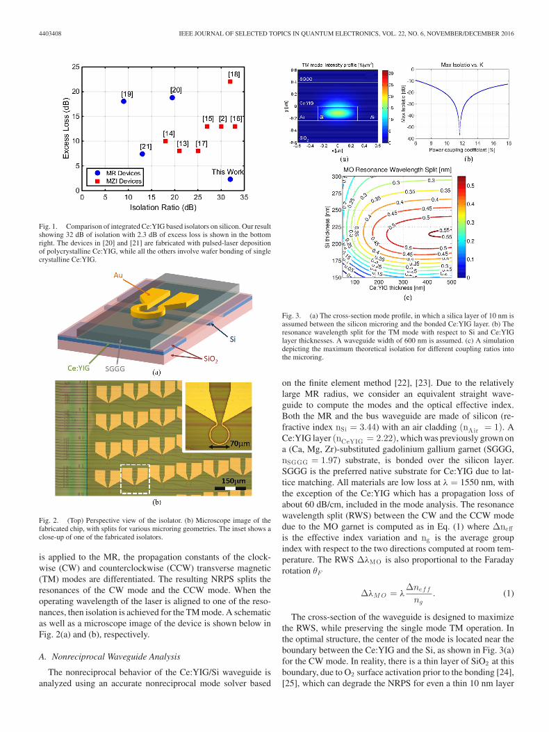
Moreover, a drawback of both MZI and MR isolators to datehas been the use of a permanent magnet to generate a staticmagnetic field, which is unattractive for integration on chip andimpedes packaging. In this work, we eliminate the need of apermanent magnet by using a metal microstrip to directly gen-erate the magnetic field above a bonded Ce:YiG/Si MR isolator.In this work, we also propose to use the same deposited metalfor thermal tuning of the MR isolator, allowing for the align-ment of the isolation wavelength, which is a critical issue forthe implementation of a narrowband device. This can correctfor fabrication errors as well as compensate for varying ambienttemperatures. Finally, the small footprint of the device keeps theexcess loss small. A summary of demonstrated integrated iso-lators using Ce:YiG on silicon is shown in Fig. 1, including theresults achieved in this work. In this figure, we plot the isolationratio of the device versus the excess loss to the silicon wave-guide of previous devices. All of these devices fundamentallyoperate for TM mode. TM isolators have been integrated with aTE-TM polarization rotator [18] for operation in TE mode.
II. DESIGN AND SIMULATION
The device is an all pass MR filter with 35 μm radius. TheCe:YIG is bonded on a silicon-on-insulator (SOI) MR that iscritically coupled to a straight bus waveguide for maximumextinction ratio [22]. When a radially outward magnetic field
1077-260X © 2016 IEEE. Personal use is permitted, but republication/redistribution requires IEEE permission.See http://www.ieee.org/publications standards/publications/rights/index.html for more information.
4403408 IEEE JOURNAL OF SELECTED TOPICS IN QUANTUM ELECTRONICS, VOL. 22, NO. 6, NOVEMBER/DECEMBER 2016
Fig. 1. Comparison of integrated Ce:YIG based isolators on silicon. Our resultshowing 32 dB of isolation with 2.3 dB of excess loss is shown in the bottomright. The devices in [20] and [21] are fabricated with pulsed-laser depositionof polycrystalline Ce:YIG, while all the others involve wafer bonding of singlecrystalline Ce:YIG.
Fig. 2. (Top) Perspective view of the isolator. (b) Microscope image of thefabricated chip, with splits for various microring geometries. The inset shows aclose-up of one of the fabricated isolators.
is applied to the MR, the propagation constants of the clock-wise (CW) and counterclockwise (CCW) transverse magnetic(TM) modes are differentiated. The resulting NRPS splits theresonances of the CW mode and the CCW mode. When theoperating wavelength of the laser is aligned to one of the reso-nances, then isolation is achieved for the TM mode. A schematicas well as a microscope image of the device is shown below inFig. 2(a) and (b), respectively.
A. Nonreciprocal Waveguide Analysis
The nonreciprocal behavior of the Ce:YIG/Si waveguide isanalyzed using an accurate nonreciprocal mode solver based
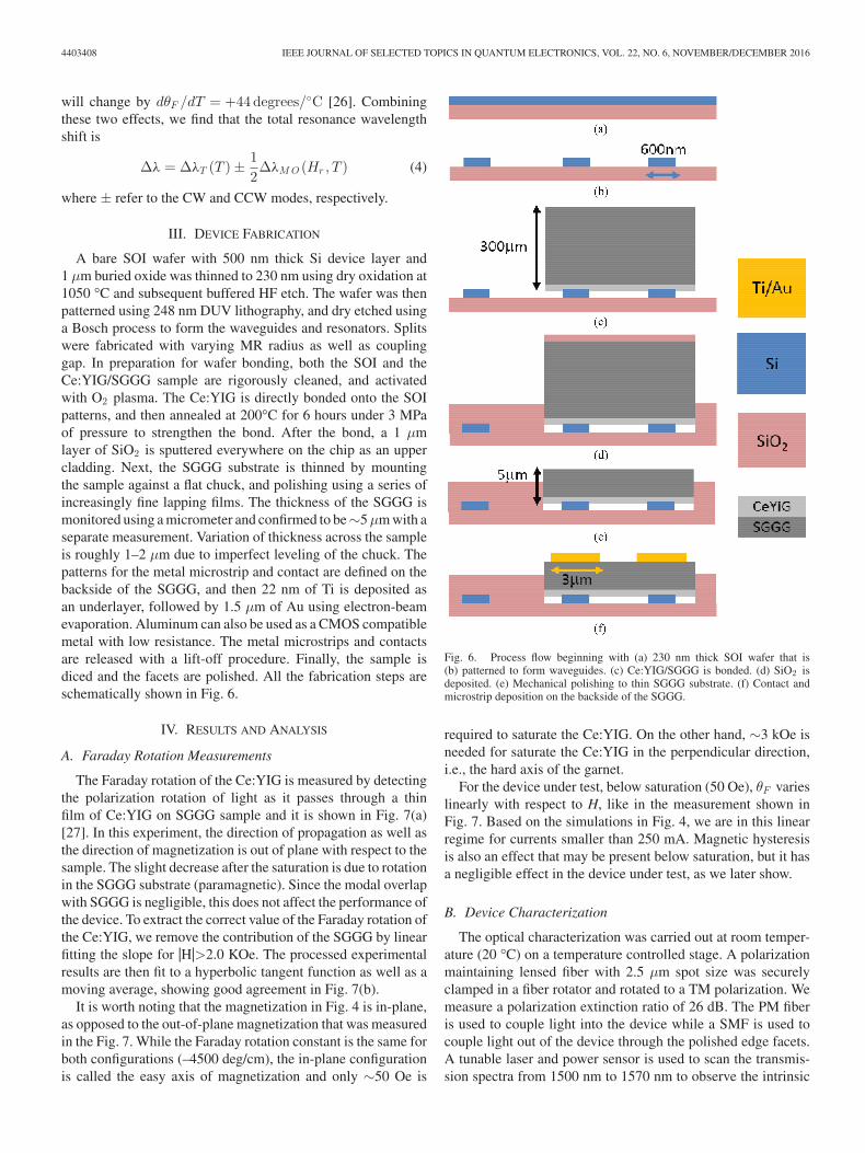
Fig. 3. (a) The cross-section mode profile, in which a silica layer of 10 nm isassumed between the silicon microring and the bonded Ce:YIG layer. (b) Theresonance wavelength split for the TM mode with respect to Si and Ce:YIGlayer thicknesses. A waveguide width of 600 nm is assumed. (c) A simulationdepicting the maximum theoretical isolation for different coupling ratios intothe microring.
on the finite element method [22], [23]. Due to the relativelylarge MR radius, we consider an equivalent straight wave-guide to compute the modes and the optical effective index.Both the MR and the bus waveguide are made of silicon (re-fractive index nSi = 3.44) with an air cladding (nAir = 1). ACe:YIG layer (nCeYIG = 2.22), which was previously grown ona (Ca, Mg, Zr)-substituted gadolinium gallium garnet (SGGG,nSGGG = 1.97) substrate, is bonded over the silicon layer.SGGG is the preferred native substrate for Ce:YIG due to lat-tice matching. All materials are low loss at λ = 1550 nm, withthe exception of the Ce:YIG which has a propagation loss ofabout 60 dB/cm, included in the mode analysis. The resonancewavelength split (RWS) between the CW and the CCW modedue to the MO garnet is computed as in Eq. (1) where Δneffis the effective index variation and ng is the average groupindex with respect to the two directions computed at room tem-perature. The RWS ΔλMO is also proportional to the Faradayrotation θF
ΔλM O = λΔnef f
ng. (1)
The cross-section of the waveguide is designed to maximizethe RWS, while preserving the single mode TM operation. Inthe optimal structure, the center of the mode is located near theboundary between the Ce:YIG and the Si, as shown in Fig. 3(a)for the CW mode. In reality, there is a thin layer of SiO2 at thisboundary, due to O2 surface activation prior to the bonding [24],[25], which can degrade the NRPS for even a thin 10 nm layer

HUANG et al.: ELECTRICALLY DRIVEN AND THERMALLY TUNABLE INTEGRATED OPTICAL ISOLATORS 4403408
of SiO2 which is assumed in the computation. Considering aFaraday rotation of Ce:YIG equal to −4500 deg/cm at roomtemperature (i.e., T = 20 °C), the RWS has been evaluated.
The maximum RWS is obtained for a 215 nm thick by600 nm wide silicon waveguide, and a 400 nm thick Ce:YIGlayer. For those values, the maximum of the field is located closeto the Ce:YIG/SiO2 /Si interfaces. For this reason, a large bendradius (i.e., 35 μm) and a thicker silicon waveguide are preferred(i.e., 230 nm) in order to keep the mode better confined and re-duce the bending loss. Our simulations predict that for a 400 nmthick layer of Ce:YIG bonded to a 230 nm tall by 600 nm wideSi waveguide with 10 nm oxide layer, the nonreciprocal RWSreaches the maximum value of 0.52 nm, as shown in Fig. 3(b).
For the proposed device, the critical power coupling coeffi-cient K is about 11.68%, which corresponds to a gap of about245 nm. The critical coupling condition is crucial for MR -basedsystems because it is related to the MR -waveguide distance,which is difficult to be experimentally controlled with highaccuracy. Due to the large propagation loss in the Ce:YIG, thecoupling condition is less strict and a variation up to 15% fromthe optimum gap can still guarantee an isolation higher than20 dB, as shown in Fig. 3(c).
B. Electromagnet Design
To provide the radially outward/inward magnetic field atthe ring-Ce:YIG interface, we apply a current through the mi-crostrip, which closely follows the shape of the ring resonator.Since the microstrip is patterned on the back of the bondedCe:YIG die, it is important to know the thickness of the SGGGsubstrate. The strength of the magnetic field in the ring is in-versely proportional to the distance between the ring and the mi-crostrip (i.e. thickness of SGGG substrate). In our simulations aswell as our actual device, we target a thickness of 5 μm. Such alayer is sufficiently thin that an applied current in the microstripgenerates a strong magnetic field at the Ce:YIG/SiO2 /Si inter-face, which induces in-plane magnetization in the Ce:YIG andcause a significant RWS. However, the SGGG is thick enoughto avoid optical loss due to overlap between the optical modeand the metallic microstrip. We computed the radial magneticfield using COMSOL Multiphysics, as shown in Fig. 4.
C. Thermal Performance
When the current is applied to the microstrip, it causes a localheating in the MR due to the Joule effect. This induces a thermalresonance wavelength shift as well as a change in the Faradayrotation. We compute the local temperature distribution in thedevice using COMSOL, as shown in Fig. 5.
By performing the modal analysis of the ring with respect tothe temperature, the thermal resonance wavelength shift ΔλT isvalued as
ΔλT =λ
ng
(∑i
∂nef f
∂ni
∂ni
∂T
)ΔT (2)
where the derivative ∂ni/∂T depends on the materials withrefractive index ni , while ∂neff /∂ni can be computed from the
Fig. 4. Simulation of the external magnetic field generated by the electriccurrent in the metal microstrip. The 3D plot shows the intensity of the radialmagnetic field in the Ce:YIG plane assuming 200 mA DC current. On the sameplane, the arrows indicate the direction of the magnetic field. In the plot onthe right, the radial component of the field with respect to the ring (denoted bythe bold arrow) as a function of the DC current in the spiral is reported.
Fig. 5. Simulation of the temperature distribution generated by the electricalcurrent. The 3D plot shows the temperature distribution in the silicon planeassuming 200 mA DC current. In the same plot, the streamlines show the currentflux in the spiral. In the plot on the right, the increment of the average temperaturein the silicon microring is reported as a function of the DC current in the spiral.
TABLE IMODAL TEMPERATURE DEPENDENCE
Material ∂ni /∂T [1/°C] ∂ne f f /∂ni
Ce:YIG 9.1 � 10−5 0.405Si 1.86 � 10−4 0.691SiO2 1.0 � 10−5 0.275Air 1.0 � 10−6 0.021
The temperature dependence of the materialrefractive index (middle column) as well asthe effect on the modal index (right column).
mode solver [23]. The results of this analysis are summarizedin the table below.
For the device under investigation, we calculate a resonancewavelength shift of 0.0716 nm/°C for the TM mode. Due to thetemperature variation, θF decreases [26] so the MO RWS is
ΔλM O (Hr , T ) =Δλ0
M O
θ0F
·[θF (Hr ) +
dθF
dT· ΔT
](3)
where θ0F = −4500◦/cm and Δλ0
M O is the corresponding RWSat room temperature. As the device heats up, the Faraday rotation
4403408 IEEE JOURNAL OF SELECTED TOPICS IN QUANTUM ELECTRONICS, VOL. 22, NO. 6, NOVEMBER/DECEMBER 2016
will change by dθF /dT = +44degrees/◦C [26]. Combiningthese two effects, we find that the total resonance wavelengthshift is
Δλ = ΔλT (T ) ± 12ΔλM O (Hr , T ) (4)
where ± refer to the CW and CCW modes, respectively.
III. DEVICE FABRICATION
A bare SOI wafer with 500 nm thick Si device layer and1 μm buried oxide was thinned to 230 nm using dry oxidation at1050 °C and subsequent buffered HF etch. The wafer was thenpatterned using 248 nm DUV lithography, and dry etched usinga Bosch process to form the waveguides and resonators. Splitswere fabricated with varying MR radius as well as couplinggap. In preparation for wafer bonding, both the SOI and theCe:YIG/SGGG sample are rigorously cleaned, and activatedwith O2 plasma. The Ce:YIG is directly bonded onto the SOIpatterns, and then annealed at 200°C for 6 hours under 3 MPaof pressure to strengthen the bond. After the bond, a 1 μmlayer of SiO2 is sputtered everywhere on the chip as an uppercladding. Next, the SGGG substrate is thinned by mountingthe sample against a flat chuck, and polishing using a series ofincreasingly fine lapping films. The thickness of the SGGG ismonitored using a micrometer and confirmed to be∼5 μm with aseparate measurement. Variation of thickness across the sampleis roughly 1–2 μm due to imperfect leveling of the chuck. Thepatterns for the metal microstrip and contact are defined on thebackside of the SGGG, and then 22 nm of Ti is deposited asan underlayer, followed by 1.5 μm of Au using electron-beamevaporation. Aluminum can also be used as a CMOS compatiblemetal with low resistance. The metal microstrips and contactsare released with a lift-off procedure. Finally, the sample isdiced and the facets are polished. All the fabrication steps areschematically shown in Fig. 6.
IV. RESULTS AND ANALYSIS
A. Faraday Rotation Measurements
The Faraday rotation of the Ce:YIG is measured by detectingthe polarization rotation of light as it passes through a thinfilm of Ce:YIG on SGGG sample and it is shown in Fig. 7(a)[27]. In this experiment, the direction of propagation as well asthe direction of magnetization is out of plane with respect to thesample. The slight decrease after the saturation is due to rotationin the SGGG substrate (paramagnetic). Since the modal overlapwith SGGG is negligible, this does not affect the performance ofthe device. To extract the correct value of the Faraday rotation ofthe Ce:YIG, we remove the contribution of the SGGG by linearfitting the slope for |H|>2.0 KOe. The processed experimentalresults are then fit to a hyperbolic tangent function as well as amoving average, showing good agreement in Fig. 7(b).
It is worth noting that the magnetization in Fig. 4 is in-plane,as opposed to the out-of-plane magnetization that was measuredin the Fig. 7. While the Faraday rotation constant is the same forboth configurations (–4500 deg/cm), the in-plane configurationis called the easy axis of magnetization and only ∼50 Oe is
Fig. 6. Process flow beginning with (a) 230 nm thick SOI wafer that is(b) patterned to form waveguides. (c) Ce:YIG/SGGG is bonded. (d) SiO2 isdeposited. (e) Mechanical polishing to thin SGGG substrate. (f) Contact andmicrostrip deposition on the backside of the SGGG.
required to saturate the Ce:YIG. On the other hand, ∼3 kOe isneeded for saturate the Ce:YIG in the perpendicular direction,i.e., the hard axis of the garnet.
For the device under test, below saturation (50 Oe), θF varieslinearly with respect to H, like in the measurement shown inFig. 7. Based on the simulations in Fig. 4, we are in this linearregime for currents smaller than 250 mA. Magnetic hysteresisis also an effect that may be present below saturation, but it hasa negligible effect in the device under test, as we later show.
B. Device Characterization
The optical characterization was carried out at room temper-ature (20 °C) on a temperature controlled stage. A polarizationmaintaining lensed fiber with 2.5 μm spot size was securelyclamped in a fiber rotator and rotated to a TM polarization. Wemeasure a polarization extinction ratio of 26 dB. The PM fiberis used to couple light into the device while a SMF is used tocouple light out of the device through the polished edge facets.A tunable laser and power sensor is used to scan the transmis-sion spectra from 1500 nm to 1570 nm to observe the intrinsic

HUANG et al.: ELECTRICALLY DRIVEN AND THERMALLY TUNABLE INTEGRATED OPTICAL ISOLATORS 4403408
Fig. 7. Faraday rotation with respect to magnetic field applied in the hard axis(out of plane). The results are shown (a) pre and (b) post data processing.
MR spectra. For more isolation measurements, a finer step of0.1 pm was used to observe the split of a single resonance.
The current was applied using a through beryllium copperprobes, and swept from 0 to 220 mA. Applying currents higherthan 250 mA resulted in permanent damage to the microstripdue to heating. At each current value, we switch from positiveto negative current to measure the RWS while maintaining thesame temperature. Switching the direction of the external mag-netic field is equivalent to switching the propagation directionof light. This is experimentally verified in the appendix. Wethen calculate the thermally induced shift by taking the averageresonance wavelength of the two spectra, and comparing thatto the spectrum of the MR when the zero current is applied.By comparing the spectra with positive and negative appliedcurrent, optical nonreciprocity and isolation can be evaluated.
Fig. 8. Spectrum measurement at I = ±80 mA. The inset shows the intrin-sic spectrum of the microring over multiple free spectral ranges without anyapplied current.
C. Measured isolation
The two transmission spectra are shown in Fig. 8 when±80 mA of current is applied, for which we measure 32 dBof isolation. The electrical power used by the isolator was9.6 mW when accounting for the measured 1.5 Ω resistanceof the microstrip. The optical loss of the device is measured bycomparing our device to a straight Si reference waveguide ofthe same dimensions, but without the bonded Ce:YIG. Of the10 dB loss, we simulate 1.2 dB of scattering loss at the interfacesbetween the channel waveguide with a silica cladding and theCe:YIG bonded waveguide using Lumerical FDTD software.The remaining 8.8 dB is due to absorption in the Ce:YIG layer.Since the length of the bus (3.5 mm) is much longer than the iso-lator (70 μm diameter) due to placement of splits on the mask asseen in Fig. 2, there are the equivalent length of eight isolators,including the microstrip and contacts, along the bus waveguide.Therefore, the excess loss of a single isolator is (1.2 + 8.8/8)= 2.3 dB. The excess loss can be further reduced by con-sidering silicon nitride cladding (n = 2) in place of silicondioxide due to a smaller refractive index contrast with theCe:YIG (n = 2.22), and smaller mode mismatch at the lateralbonded interface.
The MO RWS between CW and CCW propagation is0.16 nm, which suggests that while the magnetization of theCe:YIG is not saturated for 80 mA of current, it is more thanenough for high isolation. This is in contrast to previouslydemonstrated isolators, in which the magnetization is alwayssaturated due to the use of a strong permanent magnet. Sincethe MR is narrowband, any resonance split larger than 0.1 nmwill result in an isolation that is equal to the full extinction ra-tio of the MR, as is the case here. Therefore, a strong magnetand full saturation of the Ce:YIG magnetization is not neededfor optical isolation. The device has a 10 dB bandwidth of 1.2GHz, meaning over 22 dB of isolation is achieved in this range.This is significantly wider than semiconductor laser linewidths[28]. In externally modulated laser (EML) applications, the iso-lator can be integrated between the laser and modulator. Fordirect modulation applications, modulation induced sidebands

4403408 IEEE JOURNAL OF SELECTED TOPICS IN QUANTUM ELECTRONICS, VOL. 22, NO. 6, NOVEMBER/DECEMBER 2016
Fig. 9. The MO split and the thermal shift are shown with respect to the elec-trical current. Theoretical and experimental values are compared. In the inset,the optical isolation is reported over the full tuning range. Since the resonancewavelength initially shifts to shorter wavelengths at small currents, the curveappears to double back on itself with increasing current.
may not be isolated although they are not synchronous with thecarrier signal, which lessens their effect on RIN degradation.
D. Thermal Tuning
This microstrip approach also allows us to thermally tune theoperating wavelength by applying different amounts of current.As we sweep the current from 0 to 220 mA, we can observeboth the nonreciprocal wavelength split (MO split), as well asthe reciprocal thermally induced redshift (Therm. shift) of theresonances. From the data, the MO wavelength split saturatesat a value of 0.36 nm, which is lower than the originally pre-dicted 0.52 nm in Fig. 3(b) due to the temperature dependenceof Faraday rotation [26]. Taking into account the Joule heatingeffect, we obtain a very good agreement between the experi-mental and simulated results, as proved in Fig. 9. The tunabilityis shown in the inset in which we demonstrate 0.6 nm of tuningwhile maintaining over 20 dB of isolation, which is limited bydeviation from critical coupling and damage to the microstripat high currents. In our device, the thermal and magnetic effectsare inherently coupled because there is only one microstrip andFaraday rotation is temperature dependent. Therefore, thermaltuning also results in changing the nonreciprocal RWS. Re-ducing the coupling between the two effects by using additionalheater pads could result in higher efficiency, wider tuning ranges,and optimized control of the thermal tuning.
Hysteresis was not observed to play a strong effect in the tun-ing, as shown in Fig. 10. We imitate a hysteresis sweep by in-creasing the current from 0 to 210 mA (blue), back to 0 mA (red),down to –210 mA (green), and finally back to 0 mA (black). Wedo this in 10 mA intervals, with roughly one minute betweeneach measurement to allow temperatures to reach steady state.When we plot the resonance wavelength of the ring, we see thatthe data is consistent across the whole sweep. The plot is notsymmetric because it includes both thermal and MO effects.For positive current, the thermal effect causes redshift while the
Fig. 10. A measurement of the resonance wavelength as the current is sweptback and forth, similar to a hysteresis loop measurement. The inset shows thenonreciprocal wavelength split from MO effect.
MO effect causes blueshift. For negative current, both effectscause redshift.
The inset shows the nonreciprocal wavelength split. Thereappears to be no noticeable residual magnetization in the ma-terial, as shown by the fact that the resonance frequency whenno current is applied is the same at the beginning and the endof this measurement. There is some difference at higher cur-rents (∼0.03 nm), which could be attributed to some thermalinstability at the higher temperature.
Overall, hysteresis is weak because the magnetic fields donot fully saturate the magnetization in the garnet. Furthermore,by switching between positive and negative currents, we areconsistently switching the magnetization in the material. Webelieve this has a demagnetization effect on the material, whichlimits its hysteresis behavior.
V. CONCLUSION
In conclusion, we have demonstrated a compact integratedoptical isolator on SOI with 32 dB of isolation for the TMmode, 2.3 dB of excess loss to silicon and 0.6 nm of wave-length tuning using a current induced MO effect that consumes9.6 mW of power. This novel method does not require a perma-nent magnet and instead utilizes a deposited gold microstrip forthermal tuning as well as a source for magnetic fields. We alsopresent a model that accurately predicts the thermal, magnetic,and optical effects and interactions within the device. The devicearchitecture can be further improved by thinning the SGGG sub-strate even further for lower power consumption or selectivelyremoving the Ce:YIG on the bus waveguide to decrease loss. Webelieve that the dynamic control of magnetic fields in preciseconfigurations on chip in this approach can also be utilized inother MO devices such as MZI isolators, circulators, switches,modulators, and sensors.
APPENDIX
The direction of the magnetic field applied is always givenrelative to the propagation direction of light. In normal operationof an isolator, the propagation direction is reversed, while the

HUANG et al.: ELECTRICALLY DRIVEN AND THERMALLY TUNABLE INTEGRATED OPTICAL ISOLATORS 4403408
Fig. 11. The spectrum of the isolator for forward and backward propagatinglight under different current bias.
magnetic field is unchanged. This effect can also be observedvice versa, in which we switch the direction of the magnetic field(current) without changing the propagation direction, as the ef-fects are mathematically equivalent. We verify this in our deviceexperimentally by manually switching the propagation directionof light by changing which fiber is used as input. We expect tosee that this has the same effect as switching the magnetic field.In practice, it is difficult to maintain the exact same polarizationat the end of the two fibers. The results are shown in Fig. 11for an applied current of 100 mA. In this case, the isolator wasnot near critical coupling so the extinction ratio and isolationare not as large. Nevertheless, it is evident that +100 mA withforward optical propagation is roughly equivalent to –100 mAwith backward propagation. Similarly, +100 mA with backwardoptical propagation is very close to –100 mA in the forward di-rection. The resonance split is clearly seen in both cases andverifies the nonreciprocity in the device. The slight error in themeasurement can be attributed to not achieving identical cou-pling conditions for forwards and backwards propagation withregard to polarization. This is apparent from noticing the dif-ference between the forward and backward spectra without anyapplied current.
ACKNOWLEDGMENT
The authors would like to thank P. Morton, J. Khurgin,J. Peters, D. Spencer, M. Davenport, L. Chang, T. Komljen-ovic, and F. Di Pasquale for helpful discussions.
REFERENCES
[1] D. Jalas et al., “What is—and what is not—an optical isolator,” NaturePhoton., vol. 7, no. 8, pp. 579–582, 2013.
[2] Y. Shoji and T. Mizumoto, “Magneto-optical non-reciprocal devicesin silicon photonics,” Sci. Technol. Adv. Mater., vol. 15, no. 1, 2014,Art. no. 014602.
[3] Z. Yu and S. Fan, “Complete optical isolation created by indirect interbandphotonic transitions,” Nature Photon., vol. 3, no. 2, pp. 91–94, 2009.
[4] C. Doerr, L. Chen, and D. Vermeulen, “Silicon photonics broadbandmodulation-based isolator,” Opt. Express, vol. 22, no. 4, pp. 4493–4498,2014.
[5] H. Lira, Z. Yu, S. Fan, and M. Lipson, “Electrically driven nonreciprocityinduced by interband photonic transition on a silicon chip,” Phys. Rev.Lett., vol. 109, no. 3, 2012, Art. no. 033901.
[6] L. Tzuang, K. Fang, P. Nussenzveig, S. Fan, and M. Lipson, “Non-reciprocal phase shift induced by an effective magnetic flux for light,”Nature Photon., vol. 8, no. 9, pp. 701–705, 2014.
[7] M. Heck, S. Srinivasan, M. Davenport, and J. Bowers, “Integratedmicrowave photonic isolators: Theory, experimental realization and appli-cation in a unidirectional ring mode-locked laser diode,” Photonics, vol. 2,no. 3, pp. 957–968, 2015.
[8] S. Bhandare et al., “Novel nonmagnetic 30-dB traveling-wave single-sideband optical isolator integrated in III/V material,” IEEE J. Sel. TopicsQuantum Electron., vol. 11, no. 2, pp. 417–421, Mar./Apr. 2005.
[9] L. Fan et al., “An all-silicon passive optical diode,” Science, vol. 335,no. 6067, pp. 447–450, 2011.
[10] Y. Shi, Z. Yu, and S. Fan, “Limitations of nonlinear optical isolators dueto dynamic reciprocity,” Nature Photon., vol. 9, no. 6, pp. 388–392, 2015.
[11] C. Dong et al., “Brillouin-scattering-induced transparency and non-reciprocal light storage,” Nature Commun., vol. 6, 2015, Art. no. 6193.
[12] C. Poulton et al., “Design for broadband on-chip isolator using stimulatedBrillouin scattering in dispersion-engineered chalcogenide waveguides,”Opt. Express, vol. 20, no. 19, pp. 21235–21246, 2012.
[13] Y. Shoji, T. Mizumoto, H. Yokoi, I. Hsieh, and R. Osgood, “Magneto-optical isolator with silicon waveguides fabricated by direct bonding,”Appl. Phys. Lett., vol. 92, no. 7, 2008, Art. no. 071117.
[14] Y. Shoji, M. Ito, Y. Shirato, and T. Mizumoto, “MZI optical isolator withSi-wire waveguides by surface-activated direct bonding,” Opt. Express,vol. 20, no. 16, pp. 18440–18448, 2012.
[15] Y. Shoji, Y. Shirato, and T. Mizumoto, “Silicon mach-zehnder interfer-ometer optical isolator having 8 nm bandwidth for over 20 dB isolation,”Jpn. J. Appl. Phys., vol. 53, no. 2, 2014, Art. no. 022202.
[16] Y. Shoji, K. Miura, and T. Mizumoto, “Optical nonreciprocal devices basedon magneto-optical phase shift in silicon photonics,” J. Opt., vol. 18, no. 1,2015, Art. no. 013001.
[17] S. Ghosh et al., “Ce:YIG/silicon-on-insulator waveguide optical isolatorrealized by adhesive bonding,” Opt. Express, vol. 20, no. 2, pp. 1839–1848,2012.
[18] S. Ghosh et al., “Optical isolator for TE polarized light realized by adhesivebonding of Ce:YIG on silicon-on-insulator waveguide circuits,” IEEEPhoton. J., vol. 5, no. 3, Jun. 2013, Art. no. 6601108.
[19] M. Tien, T. Mizumoto, P. Pintus, H. Kromer, and J. E. Bowers, “Siliconring isolators with bonded nonreciprocal magneto-optic garnets,” Opt.Express, vol. 19, no. 12, pp. 11740–11745, 2011.
[20] L. Bi et al., “On-chip optical isolation in monolithically integrated non-reciprocal optical resonators,” Nature Photon., vol. 5, no. 12, pp. 758–762,2011.
[21] X. Sun et al., “Single-step deposition of cerium-substituted yttrium irongarnet for monolithic on-chip optical isolation,” ACS Photon., vol. 2, no. 7,pp. 856–863, 2015.
[22] P. Pintus, M. Tien, and J. E. Bowers, “Design of magneto-optical ring iso-lator on SOI based on the finite-element method,” IEEE Photon. Technol.Lett., vol. 23, no. 22, pp. 1670–1672, Nov. 2011.
[23] P. Pintus, “Accurate vectorial finite element mode solver for magneto-optic and anisotropic waveguides,” Opt. Express, vol. 22, no. 13,pp. 15737–15756, 2014.
[24] Y. Liu et al., “Growth of ultrathin SiO2 on Si by surface irradiationwith an O2+ Ar electron cyclotron resonance microwave plasma at lowtemperatures,” J. Appl. Phys., vol. 85, no. 3, pp. 1911–1915, 1999.
[25] D. Liang, G. Roelkens, R. Baets, and J. E. Bowers, “Hybrid integratedplatforms for silicon photonics,” Materials, vol. 3, no. 3, pp. 1782–1802,2010.
[26] K. Furuya, K. Kato, Y. Shoji, and T. Mizumoto, “Demonstration of anathermal waveguide optical isolator on silicon platform,” in Proc. Eur.Conf. Opt. Commun., 2015, pp. 1–3.
[27] T. Shintaku, U. Takehiko, and M. Kobayashi, “Magneto-optic channelwaveguides in Ce-substituted yttrium iron garnet,” J. Appl. Phys. vol. 74,no. 8, pp. 4877–4881, 1993.
[28] L. Coldren, S. Corzine, and M. Masanovic, Diode Lasers and PhotonicIntegrated Circuits, vol. 218. New York, NY, USA: Wiley, 2012.
Duanni Huang received the B.S. degree in electrical engineering fromthe Massachusetts Institute of Technology, Cambridge, MA, USA, in 2013.He received the M.S. degree in electrical engineering from the University ofCalifornia, Santa Barbara, CA, USA, in 2015, where he is currently workingtoward the Ph.D. degree. His current research interests include the field of sil-icon photonics, with an emphasis on magneto-optic and other nonreciprocalphenomenon.

4403408 IEEE JOURNAL OF SELECTED TOPICS IN QUANTUM ELECTRONICS, VOL. 22, NO. 6, NOVEMBER/DECEMBER 2016
Paolo Pintus (S’10–M’11) was born in Cagliari, Italy, in 1983. He receivedthe Bachelor’s degree (Hons.) and the Master’s degree (Hons.) in electronicengineering from the University of Cagliari, Cagliari, Italy, in 2005 and 2007,respectively, and the Ph.D. degree in innovative technologies of ICT and roboticsfrom the Scuola Superiore Sant’Anna, Pisa, Italy, in 2012. In 2007, he was aVisiting Student (Leonardo da Vinci program) in the Department of BiologicalSciences, Imperial College of London, London, U.K. From 2010 to 2011, hewas a Visiting Researcher and in 2015, he was a Visiting Assistant Project Sci-entist with the Optoelectronics Research Group, University of California SantaBarbara, Santa Barbara, CA, USA.
He is currently a Research Fellow at Scuola Superiore Sant’Anna, Pisa, Italy,and a Member of the National Inter-University Consortium for Telecommu-nications. His research interests include the field of integrated optics, siliconphotonics, and numerical method for electromagnetism.
Chong Zhang received the B.S. degree in electrical science and technologyfrom the Harbin Institute of Technology, Harbin, China, in 2007, and the M.S.degree in optical engineering from Zhejiang University, Hangzhou, China, in2010. He is currently working toward the Ph.D. degree at the University ofCalifornia, Santa Barbara, CA, USA. His research interests include epitaxialgrowth of III/V materials on silicon, photonics integration devices on hybridsilicon platform, and applications for high-speed optical interconnection.
Yuya Shoji (M’09) received the B.E., M.E., and Ph.D. degrees in electrical en-gineering from the Tokyo Institute of Technology, Tokyo, Japan, in 2003, 2005,and 2008, respectively. He was a Postdoctoral Fellow with the National Instituteof Advanced Industrial Science and Technology, Tsukuba, Japan, from 2008to 2010. He has been an Assistant Professor with the Graduate School of Sci-ence and Engineering, Tokyo Institute of Technology, from 2011 to 2014. He iscurrently an Associate Professor with the Quantum Nanoelectronics ResearchCenter, Tokyo Institute of Technology. His current research interests includedevice designs and fabrication of magneto-optical devices, silicon nano-photonic devices, and the photonic integrated circuits. He is a Member of theOptical Society of America, The Institute of Electronics, Information and Com-munication Engineers, the Japan Society of Applied Physics, and the MagneticSociety of Japan.
Tetsuya Mizumoto (S’81–M’84–F’12) received the B.E., M.E., and D.Eng.degrees in electrical engineering from the Tokyo Institute of Technology, Tokyo,Japan, in 1979, 1981, and 1984, respectively. He has been a Research Assistantat the Tokyo Institute of Technology since 1984. He is currently a Professor withthe Graduate School of Science and Engineering, Tokyo Institute of Technology.His current research interests include waveguide optical devices, especiallymagneto-optic devices.
Dr. Mizumoto received the Treatise Award in 1994 and the Best Letter Awardof Electronics Society Transactions in 2007 from the Institute of Electronics,Information and Communication Engineers (IEICE). He received the IEEEPhotonics Society Distinguished Lecturer Award in July 2009, IEEE Fellowgrade for “Contributions to investigations of waveguide optical nonreciprocaldevices for optical communications” in January 2012, and IEICE AchievementAward for “Pioneering work on optical nonreciprocal circuits” in May 2012.He is a Fellow of IEICE and a Member of the Japan Society of Applied Physicsand the Magnetic Society of Japan.
John E. Bowers (F’93) received the M.S. and Ph.D. degrees from Stanford Uni-versity, Stanford, CA, USA. He holds the Fred Kavli Chair in Nanotechnology,and is the Director of the Institute for Energy Efficiency and a Professor in theDepartment of Electrical and Computer Engineering and Materials, Universityof California, Santa Barbara (UCSB). He is a Cofounder of Aurrion, AeriusPhotonics and Calient Networks. He worked for AT& Bell Laboratories andHoneywell before joining UCSB. He is a Member of the National Academyof Engineering and a Fellow of the IEEE, OSA, and the American PhysicalSociety. He received the OSA/IEEE Tyndall Award, the OSA Holonyak Prize,the IEEE LEOS William Streifer Award, and the South Coast Business andTechnology Entrepreneur of the Year Award. He and coworkers received the EETimes Annual Creativity in Electronics Award for Most Promising Technologyfor the heterogeneous silicon laser in 2007. His research interests primarilyinclude optoelectronics and photonic integrated circuits. He has published 10book chapters, 600 journal papers, and 900 conference papers and has received54 patents.