IEEE 802.3af/at-Compliant, Powered Device Interface ...€¦ · IEEE 802.3af/at-Compliant, Powered...
16
IEEE 802.3af/at-Compliant, Powered Device Interface Controllers with Integrated Power MOSFET MAX5981A/MAX5981B _______________________________________________________________ Maxim Integrated Products 1 For pricing, delivery, and ordering information, please contact Maxim Direct at 1-888-629-4642, or visit Maxim’s website at www.maxim-ic.com. General Description The MAX5981 provides a complete interface for a pow- ered device (PD) to comply with the IEEE ® 802.3af/at standard in a power-over-ethernet (PoE) system. The MAX5981 provides the PD with a detection signature, classification signature, and an integrated isolation power switch with inrush current control. During the inrush period, the MAX5981 limits the current to less than 180mA before switching to the higher current limit (720mA to 880mA) when the isolation power MOSFET is fully enhanced. The device features an input UVLO with wide hysteresis and long deglitch time to compensate for twisted-pair cable resistive drop and to assure glitch-free transition during power-on/-off conditions. The MAX5981 can withstand up to 100V at the input. The MAX5981 supports a 2-Event classification method as specified in the IEEE 802.3at standard and provides a signal to indicate when probed by a Type 2 power sourc- ing equipment (PSE). The device detects the presence of a wall adapter power source connection and allows a smooth switch over from the PoE power source to the wall power adapter. The MAX5981 also provides a power-good (PG) signal, two-step current limit and foldback, overtemperature protection, and di/dt limit. A sleep mode feature in the MAX5981 provides low power consumption while supporting Maintain Power Signature (MPS). An ultra- low-power sleep mode feature in the MAX5981 further reduces power consumption while still supporting MPS. The MAX5981 also features an LED driver that is auto- matically activated during sleep mode. During sleep mode, the LED driver sources a periodic current (I LED ) at 250Hz (MAX5981A) or 15.625kHz (MAX5981B). The MAX5981 is available in a 16-pin, 5mm x 5mm TQFN power package. The device is rated over the -40°C to +85°C extended temperature range. Features S Sleep Mode and Ultra-Low Power S IEEE 802.3af/at Compliant S 2-Event Classification or an External Wall Adapter Indicator Output S Simplified Wall Adapter Interface S PoE Classification 0–5 S 100V Input Absolute Maximum Rating S Inrush Current Limit of 180mA Maximum S Current Limit During Normal Operation Between 720mA and 880mA S Current Limit and Foldback S Legacy UVLO at 36V S LED Driver with Programmable LED Current S Overtemperature Protection S Thermally Enhanced, 5mm x 5mm, 16-Pin TQFN Applications IEEE 802.3af/at Powered Devices IP Phones, Wireless Access Nodes, IP Security Cameras WiMAXK Base Stations 19-5732; Rev 2; 8/11 +Denotes a lead(Pb)-free/RoHS-compliant package. *EP = Exposed pad. Ordering Information WiMAX is a trademark of WiMAX Forum. IEEE is a registered service mark of the Institute of Electrical and Electronics Engineers, Inc. PART TEMP RANGE PIN- PACKAGE SLEEP MODE MAX5981AETE+ -40NC to +85NC 16 TQFN-EP* Yes MAX5981BETE+ -40NC to +85NC 16 TQFN-EP* Yes
Transcript of IEEE 802.3af/at-Compliant, Powered Device Interface ...€¦ · IEEE 802.3af/at-Compliant, Powered...

IEEE 802.3af/at-Compliant, Powered Device Interface Controllers with Integrated Power MOSFET
MA
X5
98
1A
/MA
X5
98
1B
_______________________________________________________________ Maxim Integrated Products 1
For pricing, delivery, and ordering information, please contact Maxim Direct at 1-888-629-4642, or visit Maxim’s website at www.maxim-ic.com.
General DescriptionThe MAX5981 provides a com plete interface for a pow-ered device (PD) to comply with the IEEE® 802.3af/at standard in a power-over-ethernet (PoE) system. The MAX5981 provides the PD with a detection signature, classifica tion signature, and an integrated isolation power switch with inrush current control. During the inrush period, the MAX5981 limits the current to less than 180mA before switching to the higher cur rent limit (720mA to 880mA) when the isolation power MOSFET is fully enhanced. The device features an input UVLO with wide hysteresis and long deglitch time to compensate for twisted-pair cable resistive drop and to assure glitch-free transition during power-on/-off condi tions. The MAX5981 can with stand up to 100V at the input.
The MAX5981 supports a 2-Event classification method as specified in the IEEE 802.3at standard and provides a signal to indicate when probed by a Type 2 power sourc-ing equipment (PSE). The device detects the presence of a wall adapter power source connection and allows a smooth switch over from the PoE power source to the wall power adapter.
The MAX5981 also provides a power-good (PG) signal, two-step current limit and fold back, overtemperature protection, and di/dt limit. A sleep mode feature in the MAX5981 provides low power consumption while supporting Maintain Power Signature (MPS). An ultra-low-power sleep mode feature in the MAX5981 further reduces power consump tion while still supporting MPS. The MAX5981 also features an LED driver that is auto-matically activated during sleep mode. During sleep mode, the LED driver sources a peri odic current (ILED) at 250Hz (MAX5981A) or 15.625kHz (MAX5981B).
The MAX5981 is available in a 16-pin, 5mm x 5mm TQFN power package. The device is rated over the -40°C to +85°C extended temperature range.
FeaturesS Sleep Mode and Ultra-Low Power
S IEEE 802.3af/at Compliant
S 2-Event Classification or an External Wall Adapter Indicator Output
S Simplified Wall Adapter Interface
S PoE Classification 0–5
S 100V Input Absolute Maximum Rating
S Inrush Current Limit of 180mA Maximum
S Current Limit During Normal Operation Between 720mA and 880mA
S Current Limit and Foldback
S Legacy UVLO at 36V
S LED Driver with Programmable LED Current
S Overtemperature Protection
S Thermally Enhanced, 5mm x 5mm, 16-Pin TQFN
ApplicationsIEEE 802.3af/at Powered Devices
IP Phones, Wireless Access Nodes, IP Security Cameras
WiMAXK Base Stations
19-5732; Rev 2; 8/11
+Denotes a lead(Pb)-free/RoHS-compliant package.*EP = Exposed pad.
Ordering Information
WiMAX is a trademark of WiMAX Forum.
IEEE is a registered service mark of the Institute of Electrical and Electronics Engineers, Inc.
PART TEMP RANGEPIN- PACKAGE
SLEEP MODE
MAX5981AETE+ -40NC to +85NC 16 TQFN-EP* Yes
MAX5981BETE+ -40NC to +85NC 16 TQFN-EP* Yes

IEEE 802.3af/at-Compliant, Powered Device Interface Controllers with Integrated Power MOSFET
MA
X5
98
1A
/MA
X5
98
1B
2 ______________________________________________________________________________________
Stresses beyond those listed under “Absolute Maximum Ratings” may cause permanent damage to the device. These are stress ratings only, and functional operation of the device at these or any other conditions beyond those indicated in the operational sections of the specifications is not implied. Exposure to absolute maximum rating conditions for extended periods may affect device reliability.
VDD to VSS ..........................................................-0.3V to +100VDET, RTN, WAD, PG, 2EC to VSS .......................-0.3V to +100VCLS, SL, WK, ULP, LED to VSS ...............................-0.3V to +6VMaximum Current on CLS (100ms maximum) .................100mAContinuous Power Dissipation (TA = +70NC) (Note 1) TQFN (derate 28.6mW/NC above +70NC) Multilayer Board .....................................................2285.7mW
Package Thermal Resistance (Note 2) BJA ...............................................................................35NC/W BJC .............................................................................2.7NC/WOperating Temperature Range .......................... -40NC to +85NCMaximum Junction Temperature .....................................+150NCStorage Temperature Range ............................ -65NC to +150NCLead Temperature (soldering, 10s) .............................. +300NCSoldering Temperature ................................................. +260NC
ELECTRICAL CHARACTERISTICS(VIN = (VDD - VSS) = 48V, RDET = 24.9kω, RCLS = 615ω, and RSL = 60.4kω. RTN, WAD, PG, 2EC, WK, and ULP unconnected, all voltages are referenced to VSS, unless otherwise noted. TA = TJ = -40NC to +85NC, unless otherwise noted. Typical values are at TA = +25NC.) (Note 3)
ABSOLUTE MAXIMUM RATINGS
Note 1: Maximum power dissipation is obtained using JEDEC JESD51-5 and JESD51-7 specifications.Note 2: Package thermal resistances were obtained using the method described in JEDEC specification JESD51-7, using a four-
layer board. For detailed information on package thermal considerations, refer to www.maxim-ic.com/thermal-tutorial.
PARAMETER SYMBOL CONDITIONS MIN TYP MAX UNITS
DETECTION MODE
Input Offset Current IOFFSET VIN = 1.4V to 10.1V (Note 4) 10 FA
Effective Differential Input Resistance
dRVIN = 1.4V up to 10.1V with 1V step, VDD = RTN = WAD = PG = 2EC (Note 5)
23.95 25.00 25.50 kI
CLASSIFICATION MODE
Classification Disable Threshold
VTH,CLS VIN rising (Note 6) 22.0 22.8 23.6 V
Classification Stability Time 0.2 ms
Classification Current ICLASS
VIN = 12.5V to 20.5V, VDD = RTN = WAD = PG = 2EC
Class 0, RCLS = 619I 0 3.96
mA
Class 1, RCLS = 117I 9.12 11.88
Class 2, RCLS = 66.5I 17.2 19.8
Class 3, RCLS = 43.7I 26.3 29.7
Class 4, RCLS = 30.9I 36.4 43.6
Class 5, RCLS = 21.3I 52.7 63.3
TYPE 2 (802.3at) CLASSIFICATION MODE
Mark Event Threshold VTHM VIN falling 10.1 10.7 11.6 V
Hysteresis on Mark Event Threshold
0.84 V
Mark Event Current IMARKVIN falling to enter mark event, 5.2V P VIN P 10.1V
0.25 0.85 mA
Reset Event Threshold VTHR VIN falling 2.8 4 5.2 V
POWER MODE
VIN Supply Voltage Range 60 V
VIN Supply Current IQ 0.27 0.55 mA

IEEE 802.3af/at-Compliant, Powered Device Interface Controllers with Integrated Power MOSFET
MA
X5
98
1A
/MA
X5
98
1B
_______________________________________________________________________________________ 3
ELECTRICAL CHARACTERISTICS (continued)(VIN = (VDD - VSS) = 48V, RDET = 24.9kω, RCLS = 615ω, and RSL = 60.4kω. RTN, WAD, PG, 2EC, WK, and ULP unconnected, all voltages are referenced to VSS, unless otherwise noted. TA = TJ = -40NC to +85NC, unless otherwise noted. Typical values are at TA = +25NC.) (Note 3)
PARAMETER SYMBOL CONDITIONS MIN TYP MAX UNITS
VIN Turn-On Voltage VON VIN rising 34.3 35.4 36.6 V
VIN Turn-Off Voltage VOFF VIN falling 30 V
VIN Turn-On/-Off HysteresisVHYST_UVLO
(Note 7) 4.2 V
VIN Deglitch Time tOFF_DLY VIN falling from 40V to 20V (Note 8) 30 120 Fs
Inrush to Operating Mode Delay
tDELAYtDELAY = minimum PG current pulse width after entering into power mode
87 96 105 ms
Isolation Power MOSFETOn-Resistance
RON_ISO IRTN = 600mA
TJ = +25NC 0.5 0.7
ITJ = +85NC 0.65 1
TJ = +125NC 0.8
RTN Leakage Current IRTN_LKG VRTN = 12.5V to 30V 10 FA
CURRENT LIMIT
Inrush Current Limit IINRUSHDuring initial turn-on period,VRTN = 1.5V
90 135 180 mA
Current Limit During Normal Operation
ILIMAfter inrush completed,VRTN = 1V
720 800 880 mA
Foldback Threshold VRTN (Note 9) 13 16.5 V
LOGIC
WAD Detection Threshold VWAD-REFVWAD rising, VIN = 14V to 48V (referenced to RTN)
8 9 10 V
WAD Detection Threshold Hysteresis
VWAD falling, VRTN = 0V, VSS unconnected
0.725 V
WAD Input Current IWAD-LKG VWAD = 10V (referenced to RTN) 3.5 FA
2EC Sink CurrentV2EC = 3.5V (referenced to RTN), VSS disconnected
1 1.5 2.25 mA
2EC Off-Leakage Current V2EC = 48V 1 FA
PG Sink CurrentVRTN = 1.5V, VPG = 0.8V, during inrush period
125 230 375 FA
PG Off-Leakage Current VPG = 60V 1 FA
SLEEP MODE
WK and ULP Logic Threshold VTH VWK falling and VULP rising and falling 1.5 3 V
SL Logic Threshold Falling 0.75 0.8 0.85 V
SL Current RSL = 0I 140 FA
LED Current Amplitude ILED
RSL = 60.4kI, VLED = 3.5V 10 10.5 11.5
mARSL = 30.2kI, VLED = 3.75V 19.5 20.9 22.5
RSL = 30.2kI, VLED = 4V 19

IEEE 802.3af/at-Compliant, Powered Device Interface Controllers with Integrated Power MOSFET
MA
X5
98
1A
/MA
X5
98
1B
4 ______________________________________________________________________________________
ELECTRICAL CHARACTERISTICS (continued)(VIN = (VDD - VSS) = 48V, RDET = 24.9kω, RCLS = 615ω, and RSL = 60.4kω. RTN, WAD, PG, 2EC, WK, and ULP unconnected, all voltages are referenced to VSS, unless otherwise noted. TA = TJ = -40NC to +85NC, unless otherwise noted. Typical values are at TA = +25NC.) (Note 3)
Note 3: All devices are 100% production tested at TA = +25NC. Limits over temperature are guaranteed by design.Note 4: The input offset current is illustrated in Figure 1.Note 5: Effective differential input resistance is defined as the differential resistance between VDD and VSS. See Figure 1.Note 6: Classification current is turned off whenever the device is in power mode.Note 7: UVLO hysteresis is guaranteed by design, not production tested.Note 8: A 20V glitch on input voltage, which takes VDD below VON shorter than or equal to tOFF_DLY does not cause the
MAX5981A/MAX5981B to exit power-on mode.Note 9: In power mode, current-limit foldback is used to reduce the power dissipation in the isolation MOSFET during an overload
condition across VDD and RTN.
Figure 1. Effective Differential Input Resistance/Offset Current
PARAMETER SYMBOL CONDITIONS MIN TYP MAX UNITS
LED Current Programmable Range
10 20 mA
LED Current with Grounded SL VSL = 0V 20.5 24.5 28.5 mA
LED Current Frequency fILEDNormal and ULP sleep mode
MAX5981A 250 Hz
MAX5981B 15.625 kHz
LED Current Duty Cycle DILED Normal and ULP sleep mode 25 %
VDD Current Amplitude IVDD Normal sleep mode, VLED = 3.5V 10 11 12 mA
Internal Current Duty Cycle DIVDD Normal and ULP sleep modes 75 %
Internal Current Enable Time tMPS ULP sleep mode 76 84 92 ms
Internal Current Disable Time tMPDO ULP sleep mode 205 228 250 ms
THERMAL SHUTDOWN
Thermal-Shutdown Threshold TSD TJ rising +140 NC
Thermal-Shutdown Hysteresis TJ falling 28 NC
IIN
IINi + 1
IINi
IOFFSET
dRi
1VVINi VINi + 1
IOFFSET = IINi - VINi
dRi
dRi = (VINi + 1 - VINi)
= 1V
(IINi + 1 - IINi)
(IINi + 1 - IINi)
VIN

IEEE 802.3af/at-Compliant, Powered Device Interface Controllers with Integrated Power MOSFET
MA
X5
98
1A
/MA
X5
98
1B
_______________________________________________________________________________________ 5
Typical Operating Characteristics(VIN = (VDD - VSS) = 54V, RDET = 24.9kω, RCLS = 615ω, and RSL = 60.4kω. RTN, WAD, PG, 2EC, WK, and ULP unconnected; all voltages are referenced to VSS.)
DETECTION CURRENTvs. INPUT VOLTAGE
MAX
5981
toc0
1
VIN (V)
I IN (m
A)
8642
0.1
0.2
0.3
0.4
0.5
00 10
IIN = IVDD + IDETRDET = 25.4kIRTN = 2EC = PG = WAD = VDD-40°C P TA P +85NC
SIGNATURE RESISTANCEvs. INPUT VOLTAGE
R SIG
NATU
RE (kI
)
8642
24.5
25.0
25.5
26.0
24.00 10
MAX
5981
toc0
2
VIN (V)
IIN = IVDD + IDETRDET = 24.9kIRTN = 2EC = PG = WAD = VDD
TA = -40NC
TA = +85NC
TA = +25NC
INPUT OFFSET CURRENTvs. INPUT VOLTAGE
INPU
T OF
FSET
CUR
RENT
(FA)
8642
-2
0
2
4
-40 10
MAX
5981
toc0
3
VIN (V)
TA = +85NCTA = -40NC
TA = +25NC
CLASSIFICATION CURRENT vs.INPUT VOLTAGE
MAX
5981
toc0
4
VIN (V)
I IN (m
A)
252015105
10
20
30
40
50
60
70
00 30
CLASS 5
CLASS 4
CLASS 3
CLASS 2
CLASS 1
CLASS 0
CLASSIFICATION SETTLING TIMEMAX5981 toc05
VIN10V/div
IIN200mA/div
VCLS1V/div
100Fs/div
RCLS = 30.9I
2EC SINK CURRENT vs. 2EC VOLTAGE
V2EC (V)
I 2EC
(mA)
5040302010
0.4
0.8
1.2
1.6
2.0
00 60
MAX
5981
toc0
6
VSS FLOATINGV2EC REFERENCED TO RTNVWAD = 14V
TA = -40NC
TA = +85NC
TA = +25NC
PG SINK CURRENT vs. PG VOLTAGE
VPG (V)
I PG
(FA)
5040302010
100
150
200
250
300
500 60
MAX
5981
toc0
7
TA = -40NC
TA = +85NC
TA = +25NC
INRUSH CURRENT LIMITvs. RTN VOLTAGE
MAX
5981
toc0
8
VRTN (V)
INRU
SH C
URRE
NT L
IMIT
(mA)
5040302010
70
90
110
130
150
500 60

IEEE 802.3af/at-Compliant, Powered Device Interface Controllers with Integrated Power MOSFET
MA
X5
98
1A
/MA
X5
98
1B
6 ______________________________________________________________________________________
Typical Operating Characteristics (continued)(VIN = (VDD - VSS) = 54V, RDET = 24.9kω, RCLS = 615ω, and RSL = 60.4kω. RTN, WAD, PG, 2EC, WK, and ULP unconnected; all voltages are referenced to VSS.)
INRUSH CONTROL WAVEFORM WITHTYPE 2 CLASSIFICATION
MAX5981 toc10
0V
0V
0V
0A
0V
VRTN50V/div
IRTN100mA/div
VDD50V/div
VPG10V/div
V2EC40V/div
20ms/div
USING TYPICAL APPLICATION CIRCUIT2EC PULLED UP TO VDD WITH 10kI
INRUSH CONTROL WAVEFORM WITHTYPE 2 CLASSIFICATION
MAX5981 toc11
VPG10V/div0V
0V
0V
0A
0V
VRTN50V/div
IRTN200mA/div
VDD50V/div
20ms/div
V2EC40V/div
USING TYPICAL APPLICATION CIRCUIT2EC PULLED UP TO VDD WITH 10kI
LED CURRENT vs. RSL
RSL (kI)
I LED
(mA)
60555045403530252015105
13
16
19
22
25
100 65
MAX
5981
toc1
2
-40NC < TA < +85NC
LED CURRENT vs. LED VOLTAGE
I LED
(mA)
4321
10
15
20
25
50 5
MAX
5981
toc1
3
VLED (V)
RSL = 60.4kI
RSL = 30.2kI
NORMAL OPERATION CURRENT LIMITvs. RTN VOLTAGE
MAX
5981
toc0
9
VRTN (V)
CURR
ENT
LIM
IT (m
A)
504010 20 30
200
300
400
500
600
700
800
900
1000 60
IEEE 802.3af/at-Compliant, Powered Device Interface Controllers with Integrated Power MOSFET
MA
X5
98
1A
/MA
X5
98
1B
_______________________________________________________________________________________ 7
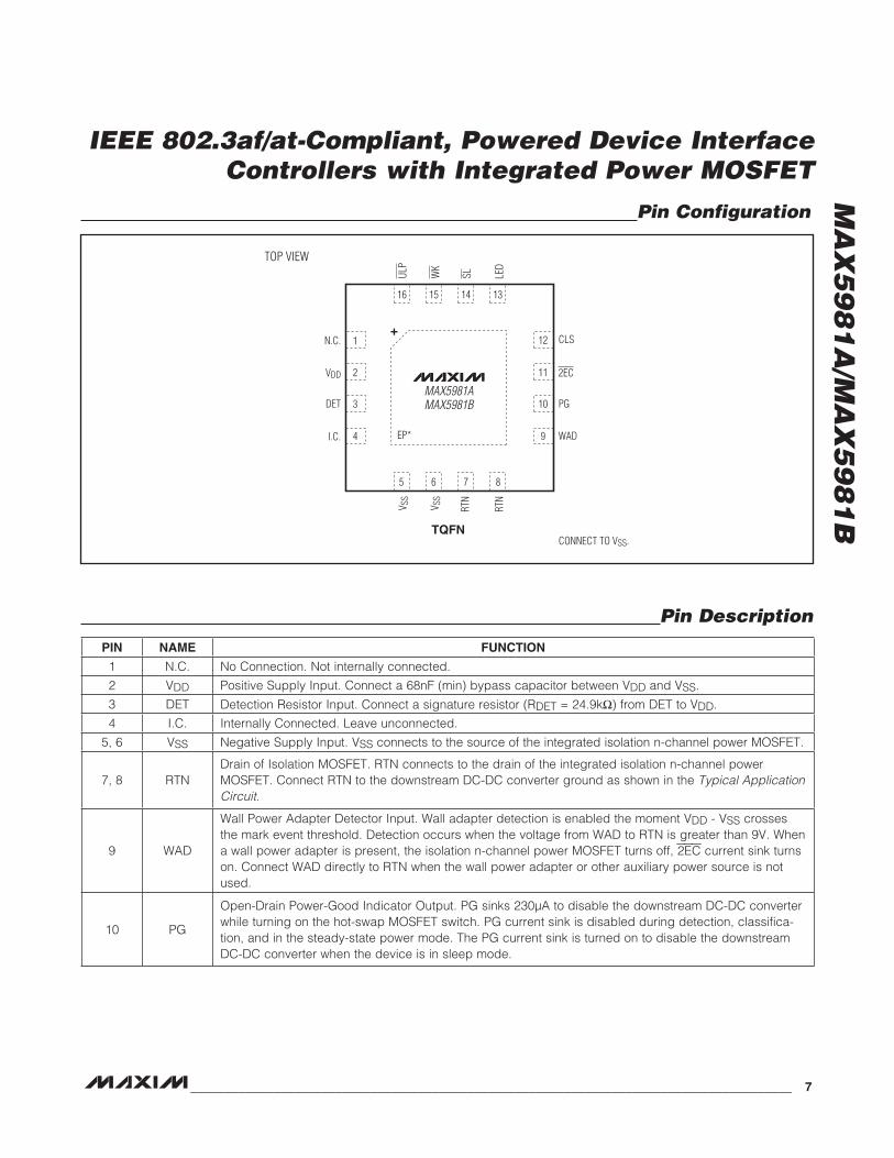
Pin Description
PIN NAME FUNCTION
1 N.C. No Connection. Not internally connected.
2 VDD Positive Supply Input. Connect a 68nF (min) bypass capacitor between VDD and VSS.
3 DET Detection Resistor Input. Connect a signature resistor (RDET = 24.9kI) from DET to VDD.
4 I.C. Internally Connected. Leave unconnected.
5, 6 VSS Negative Supply Input. VSS connects to the source of the integrated isolation n-channel power MOSFET.
7, 8 RTNDrain of Isolation MOSFET. RTN connects to the drain of the integrated isolation n-channel power MOSFET. Connect RTN to the downstream DC-DC converter ground as shown in the Typical Application Circuit.
9 WAD
Wall Power Adapter Detector Input. Wall adapter detection is enabled the moment VDD - VSS crosses the mark event threshold. Detection occurs when the voltage from WAD to RTN is greater than 9V. When a wall power adapter is present, the isolation n-channel power MOSFET turns off, 2EC current sink turns on. Connect WAD directly to RTN when the wall power adapter or other auxiliary power source is not used.
10 PG
Open-Drain Power-Good Indicator Output. PG sinks 230FA to disable the downstream DC-DC converter while turning on the hot-swap MOSFET switch. PG current sink is disabled during detection, classifica-tion, and in the steady-state power mode. The PG current sink is turned on to disable the downstream DC-DC converter when the device is in sleep mode.
Pin Configuration
3
4
2
1
10
9
11
V SS
RTN
V SS
EP*
LED
5 6
VDD
8
16 15 13
DET
I.C.
CLS
2EC
PG
WAD
MAX5981AMAX5981B
RTN
7
14
N.C.
TQFN
12
ULP
WK
SL
CONNECT TO VSS.
+
TOP VIEW

IEEE 802.3af/at-Compliant, Powered Device Interface Controllers with Integrated Power MOSFET
MA
X5
98
1A
/MA
X5
98
1B
8 ______________________________________________________________________________________
Pin Description (continued)
PIN NAME FUNCTION
11 2EC
2-Event Classification Detect or Wall Adapter Detect Output. A 1.5mA current sink is enabled at 2EC when a Type 2 PSE or a wall adapter is detected. When powered by a Type 2 PSE, the 2EC current sink is enabled after the isolation MOSFET is fully on until VIN drops below the UVLO threshold. 2EC is latched when powered by a Type 2 PSE until VIN drops below the reset threshold. 2EC also asserts when a wall adapter supply, typically greater than 9V, is applied between WAD and RTN. 2EC is not latched if asserted by WAD. The 2EC current sink is turned off when the device is in sleep mode.
12 CLSClassification Resistor Input. Connect a resistor (RCLS) from CLS to VSS to set the desired classification current. See the classification current specifications in the Electrical Characteristics table to find the resistor value for a particular PD classification.
13 LEDLED Driver Output. During sleep mode, LED sources a periodic current (ILED). The amplitude of ILED is set by RSL according to the formula ILED (in A) = 645.75/(RSL + 1200).
14 SLSleep Mode Enable Input. A falling edge on SL brings the device into sleep mode (VSL must drop below 0.75V). An external resistor (RSL) connected between SL and VSS sets the LED current (ILED).
15 WKWake Mode Enable Input. WK has an internal 2.5kI pullup resistor to the internal 5V bias rail. A falling edge on WK brings the device out of sleep mode and into the normal operating mode (wake mode).
16 ULP
Ultra-Low-Power Enable Input (in Sleep Mode). ULP has an internal 50kI pullup resistor to the internal 5V bias rail. A falling edge on SL while ULP is asserted low enables ultra-low-power mode. When ultra-low-power mode is enabled, the power consumption of the device is reduced even lower than normal sleep while still supporting MPS.
–– EPExposed Pad. Do not use EP as an electrical connection to VSS. EP is internally connected to VSS through a resistive path and must be connected to VSS externally. To optimize power dissipation, solder the exposed pad to a large copper power plane.

IEEE 802.3af/at-Compliant, Powered Device Interface Controllers with Integrated Power MOSFET
MA
X5
98
1A
/MA
X5
98
1B
_______________________________________________________________________________________ 9
Simplified Block Diagram
1.5mA
46µA
VDD
EN CLS
2EC
VDD
5V
D Q
Q
SET
CLR
DET
VSS
5V REGULATOR
THERMAL SHUTDOWN
QR
S
VDD
VDD
VDD
WAD
RTN
LED
VON/VOFF
VDD
D Q
Q
SET
CLR
9V
230µA
PG
CLASSIFICATION
ISWITCH
LOGIC
K x ISWITCH
ISOLATIONSWITCH
S
MUX
I0
I11/K MAX5981A
MAX5981B
SL
WK
ULP
5V
50kI
5V
2.5kI
tDELAY

IEEE 802.3af/at-Compliant, Powered Device Interface Controllers with Integrated Power MOSFET
MA
X5
98
1A
/MA
X5
98
1B
10 _____________________________________________________________________________________
Typical Operating Circuit
2-EVENTCLASSIFICATION
DETECTION
-54V
MAX5981AMAX5981B
1kI
VDD
RTN
WAD
PG
2EC/WAD
2EC
24V/48VBATTERY
1.5mA
WK SL
ULP
LED
-54V
-54V
-54V
ISOLATED SLEEPMODE INPUT
ISOLATED ULPMODE INPUT
68nF
RJ-45AND
BRIDGE RECTIFIER
GND
SMAJ58A
RDET24.9kI
RCLS
VSS
DET
CLS
ENABLE
DC-DCCONVERTER
IN+
IN-
GND

IEEE 802.3af/at-Compliant, Powered Device Interface Controllers with Integrated Power MOSFET
MA
X5
98
1A
/MA
X5
98
1B
______________________________________________________________________________________ 11
Detailed DescriptionOperating Modes
Depending on the input voltage (VIN = VDD - VSS), the MAX5981 operates in four differ ent modes: PD detec-tion, PD classification, mark event, and PD power. The devices enter PD detection mode when the input voltage is between 1.4V and 10.1V. The device enters PD clas-sification mode when the input voltage is between 12.6V and 20V. The device enters PD power mode once the input voltage exceeds VON.
Detection Mode (1.4V P VIN P 10.1V)In detection mode, the power source equipment (PSE) applies two voltages on VIN in the 1.4V to 10.1V range (1V step minimum) and then records the current measure ments at the two points. The PSE then computes DV/DI to ensure the presence of the 24.9kI signature resistor. Connect the signature resistor (RDET) from VDD to DET for proper signature detection. The MAX5981 pulls DET low in detection mode. DET goes high imped-ance when the input voltage exceeds 12.5V. In detection mode, most of the MAX5981 internal circuitry is off and the offset current is less than 10µA.
If the voltage applied to the PD is reversed, install pro-tection diodes at the input terminal to prevent internal damage to the MAX5981 (see the Typical Application Circuit). Since the PSE uses a slope technique (DV/DI) to calculate the signature resistance, the DC offset due to the protection diodes is subtracted and does not affect the detection process.
Classification Mode (12.6V P VIN P 20V)In the classification mode, the PSE classifies the PD based on the power consumption required by the PD.
This allows the PSE to efficiently manage power distribu-tion. Class 0–5 is defined as shown in Table 1. (The IEEE 802.3af/at standard defines only Class 0–4 and Class 5 for any spe cial requirement.) An external resistor (RCLS) connected from CLS to VSS sets the classification current.
The PSE determines the class of a PD by applying a volt-age at the PD input and measuring the current sourced out of the PSE. When the PSE applies a voltage between 12.6V and 20V, the MAX5981A/MAX5981B exhibit a cur-rent characteristic with a value shown in Table 1. The PSE uses the classification current informa tion to classify the power requirement of the PD. The classification cur-rent includes the current drawn by RCLS and the supply current of the MAX5981A/MAX5981B so the total current drawn by the PD is within the IEEE 802.3af/at standard figures. The classification current is turned off whenever the device is in power mode.
2-Event Classification and DetectionDuring 2-Event classification, a Type 2 PSE probes PD for classification twice. In the first classification event, the PSE presents an input voltage between 12.6V and 20.5V and the MAX5981A/MAX5981B pres ent the pro-grammed load ICLASS. The PSE then drops the probing voltage below the mark event threshold of 10.1V and the MAX5981A/MAX5981B pres ent the mark current (IMARK). This sequence is repeated one more time.
When the MAX5981A/MAX5981B are pow ered by a Type 2 PSE, the 2-Event identification output 2EC asserts low after the internal isolation n-channel MOSFET is fully turned on. 2EC current sink is turned off when VDD goes below the UVLO threshold (VOFF) and turns on when VDD goes above the UVLO threshold (VON), unless VDD goes below VTHR to reset the latched output of the
Table 1. Setting Classification Current
*VIN is measured across the MAX5981A/MAX5981B input VDD to VSS.
CLASS
MAXIMUM POWER USED
BY PD(W)
RCLS(I)
VIN*(V)
CLASS CURRENT SEEN AT VIN (mA)
IEEE 802.3at PD CLASSIFICATION CURRENT
SPECIFICATION (mA)
MIN MAX MIN MAX
0 0.44 to 12.95 615 12.6 to 20 0 4 0 5
1 0.44 to 3.84 117 12.6 to 20 9 12 8 13
2 3.84 to 6.49 66.5 12.6 to 20 17 20 16 21
3 6.49 to 12.95 43.7 12.6 to 20 26 30 25 31
4 12.95 to 25.5 30.9 12.6 to 20 36 44 35 45
5 > 25.5 21.3 12.6 to 20 54 64 51 68

IEEE 802.3af/at-Compliant, Powered Device Interface Controllers with Integrated Power MOSFET
MA
X5
98
1A
/MA
X5
98
1B
12 _____________________________________________________________________________________
Type 2 PSE detection flag. Alternatively, the 2EC output also serves as a wall adapt er detection output when the MAX5981A/MAX5981B are powered by an external wall power adapter. See the Wall Power Adapter Detection and Operation section for more information.
Power Mode (Wake Mode)The MAX5981A/MAX5981B enter power mode when VIN rises above the undervoltage lock out threshold (VON). When VIN rises above VON, the MAX5981A/MAX5981B turn on the internal n-channel isolation MOSFET to con-nect VSS to RTN with inrush current limit internally set to 135mA (typ). The iso lation MOSFET is fully turned on when the voltage at RTN is near VSS and the inrush cur-rent is reduced below the inrush limit. Once the isolation MOSFET is fully turned on, the MAX5981A/MAX5981B change the cur rent limit to 800mA. The open-drain power-good output (PG) remains low for a minimum of tDELAY until the power MOSFET fully turns on to keep the downstream DC-DC converter disabled during inrush.
Undervoltage LockoutThe MAX5981A/MAX5981B operate up to a 60V supply voltage with a turn-on UVLO threshold (VON) at 35.4V and a turn-off UVLO threshold (VOFF) at 31V. When the input voltage is above VON, the MAX5981A/MAX5981B enter power mode and the inter nal MOSFET is turned on. When the input voltage goes below VOFF for more than tOFF_DLY, the MOSFET turns off.
Sleep and Ultra-Low-Power Sleep ModesThe MAX5981A/MAX5981B feature a sleep mode, which pulls PG low while keeping the internal n-channel isola-tion MOSFET turned on. The PG output is used to dis-able downstream DC-DC converters reducing the power consumption of the overall PD system in sleep mode. In sleep mode, the LED driver output (LED) sources peri-odic current pulses. The LED current ILED is set by an external resistor RSL, see the Applications Information section for more information.
An ultra-low-power sleep mode allows the MAX5981A/MAX5981B to further reduce power consumption while maintaining the power signature of the standard. The ultra-low-power enable input ULP is internally held high with a 50kI pullup resistor to the internal 5V bias of the MAX5981A/MAX5981B. Set ULP to logic-low and apply a falling edge to SL to enable ultra-low-power sleep mode. Apply a falling edge on the wake-mode enable input (WK) to disable sleep or ultra-low-power sleep mode and resume normal operation.
LED DriverThe MAX5981A/MAX5981B drive an LED connected from the output LED to VSS. During sleep mode/ultra-low-power sleep mode, the LED is driven by current pulses with the amplitude set by the resistor connected from SL to VSS. The LED driver current ampli tude is program-mable from 10mA to 20mA using RSL according to the following formula:
LED645.75
I (in amperes)R 1200
=+SL
Power-Good OutputAn open-drain output (PG) is used to allow disabling downstream DC-DC converter until the n-channel isola-tion MOSFET is fully turned on. PG is pulled low to VSS for a period of tDELAY and until the internal isolation MOSFET is fully turned on. The PG is also pulled low during sleep mode and coming out of thermal shutdown.
Thermal-Shutdown ProtectionThe MAX5981A/MAX5981B include thermal protection from excessive heating. If the junction tempera ture exceeds the thermal-shutdown threshold of +140NC, the MAX5981A/MAX5981B turn off the internal power MOSFET, LED driver, and 2EC current sink. When the junction temperature falls below +112NC, the device enters inrush mode and then return to power mode. Inrush mode ensures the downstream DC-DC converter is turned off as the internal power MOSFET is turned on.
Wall Power Adapter Detection and OperationFor applications where an auxiliary power source such as a wall power adapter is used to power the PD, the MAX5981A/MAX5981B feature wall power adapter detection. The MAX5981A/MAX5981B give highest prior-ity to the WAD and smooth ly switch the power supply to WAD when it is detected. Once the input voltage (VDD - VSS) exceeds the mark event threshold, the MAX5981A/MAX5981B enable wall adapter detection. The wall power adapt er is connected from WAD to RTN. The MAX5981A/MAX5981B detect the wall power adapter when the voltage from WAD to RTN is greater than 9V. When a wall power adapter is detected, the internal n-channel isolation MOSFET turns off, 2EC current sink turns on, and classification current is disabled if VIN is in the classification range.
IEEE 802.3af/at-Compliant, Powered Device Interface Controllers with Integrated Power MOSFET
MA
X5
98
1A
/MA
X5
98
1B
______________________________________________________________________________________ 13
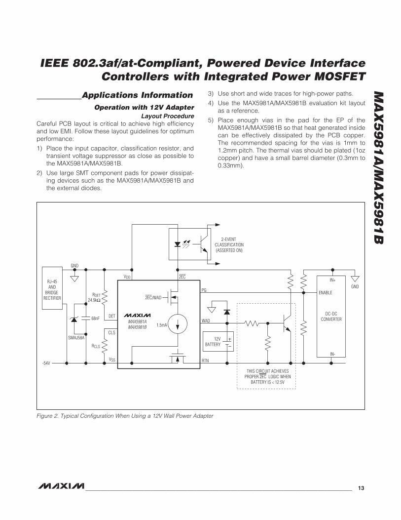
Applications InformationOperation with 12V Adapter
Layout ProcedureCareful PCB layout is critical to achieve high efficiency and low EMI. Follow these layout guidelines for optimum performance:
1) Place the input capacitor, classification resistor, and transient voltage suppressor as close as possible to the MAX5981A/MAX5981B.
2) Use large SMT component pads for power dissipat-ing devices such as the MAX5981A/MAX5981B and the external diodes.
3) Use short and wide traces for high-power paths.
4) Use the MAX5981A/MAX5981B evaluation kit layout as a reference.
5) Place enough vias in the pad for the EP of the MAX5981A/MAX5981B so that heat generated inside can be effectively dissipated by the PCB copper. The recommended spacing for the vias is 1mm to 1.2mm pitch. The thermal vias should be plated (1oz copper) and have a small barrel diameter (0.3mm to 0.33mm).
Figure 2. Typical Configuration When Using a 12V Wall Power Adapter
68nF
2-EVENT CLASSIFICATION(ASSERTED ON)
ENABLE
DC-DCCONVERTER
IN+
IN-
RJ-45AND
BRIDGE RECTIFIER
GND
GND
-54V
SMAJ58A
MAX5981AMAX5981B
RDET24.9kI
RCLS
VDD
VSS RTN
WAD
PG
DET
CLS
2EC/WAD
2EC
12VBATTERY
1.5mA
THIS CIRCUIT ACHIEVES PROPER 2EC LOGIC WHEN
BATTERY IS < 12.5V

IEEE 802.3af/at-Compliant, Powered Device Interface Controllers with Integrated Power MOSFET
MA
X5
98
1A
/MA
X5
98
1B
14 _____________________________________________________________________________________
Typical Application Circuit
68nF
ISOLATED 2-EVENTCLASSIFICATION
OUTPUTGND
VAC
VAC
GND
-54V
SMAJ58A
WALK MODEINPUT
MAX5981AMAX5981B
24.9kI
43.7I
60.4kI
1kI
VDD
VSS RTN
WAD
PGPG
DET
CLS
2EC/WAD
2EC
24/48VBATTERY
1.4mA
WK SL
ULP
LED
-54V
RTN
-54V
-54V
ISOLATED SLEEPMODE INPUT
ISOLATED ULPMODE INPUT
MAX15000
ULVO/EN IN
VCCUFLG
FB
COMP
CS
PG
CS
VCC
VCC
CS
RTN
ISOLATED +5.3V/2A
ISOLATED RTN
ISOLATED RTN
GNDRTN
GND 33kI
10kI
249I
22.1I
0.75I
1kI
619I 8.2nF
330pF
649I
4.99kI1kI 100pF
33nF
8.06kI
2.49kI
1kI18.1kI
RTN
4.99kI
NDRV
GND
RT
51.5kI1.37MI 0.1µF
0.1µF 0.1µF
0.1µF
22µF
4.7µF
2.2nF
8.06kI

IEEE 802.3af/at-Compliant, Powered Device Interface Controllers with Integrated Power MOSFET
MA
X5
98
1A
/MA
X5
98
1B
______________________________________________________________________________________ 15
Package InformationFor the latest package outline information and land patterns, (footprints) go to www.maxim-ic.com/packages. Note that a “+”, “#”, or “-” in the package code indicates RoHS status only. Package drawings may show a different suffix character, but the drawing pertains to the package regardless of RoHS status.
Chip InformationPROCESS: BiCMOS
PACKAGE TYPE
PACKAGE CODE
OUTLINENO.
LAND PATTERN NO.
16 TQFN-EP T1655+4 21-0140 90-0121

IEEE 802.3af/at-Compliant, Powered Device Interface Controllers with Integrated Power MOSFET
MA
X5
98
1A
/MA
X5
98
1B
Maxim cannot assume responsibility for use of any circuitry other than circuitry entirely embodied in a Maxim product. No circuit patent licenses are implied. Maxim reserves the right to change the circuitry and specifications without notice at any time.
16 Maxim Integrated Products, 120 San Gabriel Drive, Sunnyvale, CA 94086 408-737-7600© 2011 Maxim Integrated Products Maxim is a registered trademark of Maxim Integrated Products, Inc.
Revision History
REVISION NUMBER
REVISION DATE
DESCRIPTIONPAGES
CHANGED
0 1/11 Initial release —
1 8/11Revised General Description, Absolute Maximum Ratings, Electrical Characteristics, Pin Description, Typical Operating Circuit, LED Driver section, and Typical Application Circuit.
1–8, 10, 11, 12, 14
2 8/11Revised General Description, Electrical Characteristics, Typical Operating Characteristics, and Pin Description.
1, 4, 6, 8