
IDSH1G–02A1F1C IDSH1G–03A1F1C IDSH1G–04A1F1C · Page 42 Added new table Table 35...
49
IDSH1G–02A1F1C IDSH1G–03A1F1C IDSH1G–04A1F1C 1-Gbit Double-Data-Rate-Three SDRAM DDR3 SDRAM EU RoHS Compliant Products Advance Internet Data Sheet Rev. 0.63 June 2008
Transcript of IDSH1G–02A1F1C IDSH1G–03A1F1C IDSH1G–04A1F1C · Page 42 Added new table Table 35...

June 2008
IDSH1G–02A1F1CIDSH1G–03A1F1CIDSH1G–04A1F1C 1-Gbit Double-Data-Rate-Three SDRAM DDR3 SDRAMEU RoHS Compl iant Products
Advance
Internet Data Sheet Rev. 0.63
Advance Internet Data Sheet
IDSH1G–0[2/3/4]A1F1C1-Gbit Double-Data-Rate-Three SDRAM
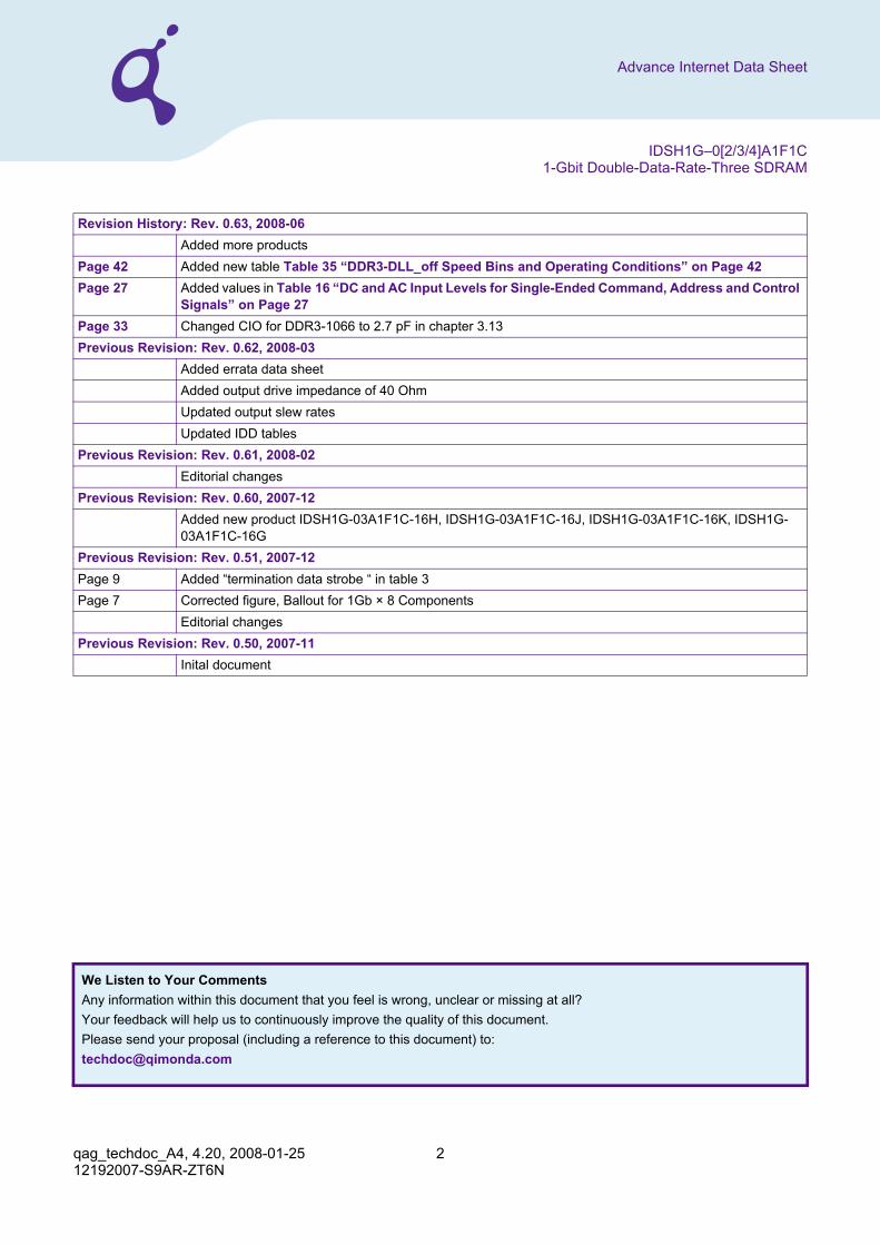
Revision History: Rev. 0.63, 2008-06Added more products
Page 42 Added new table Table 35 “DDR3-DLL_off Speed Bins and Operating Conditions” on Page 42Page 27 Added values in Table 16 “DC and AC Input Levels for Single-Ended Command, Address and Control
Signals” on Page 27Page 33 Changed CIO for DDR3-1066 to 2.7 pF in chapter 3.13Previous Revision: Rev. 0.62, 2008-03
Added errata data sheetAdded output drive impedance of 40 OhmUpdated output slew ratesUpdated IDD tables
Previous Revision: Rev. 0.61, 2008-02Editorial changes
Previous Revision: Rev. 0.60, 2007-12Added new product IDSH1G-03A1F1C-16H, IDSH1G-03A1F1C-16J, IDSH1G-03A1F1C-16K, IDSH1G-03A1F1C-16G
Previous Revision: Rev. 0.51, 2007-12Page 9 Added “termination data strobe “ in table 3Page 7 Corrected figure, Ballout for 1Gb × 8 Components
Editorial changesPrevious Revision: Rev. 0.50, 2007-11
Inital document
qag_techdoc_A4, 4.20, 2008-01-25 212192007-S9AR-ZT6N
We Listen to Your CommentsAny information within this document that you feel is wrong, unclear or missing at all?Your feedback will help us to continuously improve the quality of this document.Please send your proposal (including a reference to this document) to:[email protected]

IDSH1G–0[2/3/4]A1F1C1-Gbit Double-Data-Rate-Three SDRAM
Advance Internet Data Sheet
1 Overview
This chapter gives an overview of the Double-Data-Rate-Three (DDR3) SDRAM component product family and describes itsmain characteristics.
1.1 FeaturesThe DDR3 SDRAM offers the following key features:• 1.5 V ± 0.075 V supply voltage for VDD and VDDQ• SDRAM configurations with ×4, ×8 and ×16 data in/outputs• Eight internal banks for concurrent operation• 8-Bit prefetch architecture• Page Size:1 kByte page size for ×4 and ×8; 2 kByte page
size for ×16 components• Asynchronous RESET • Auto-Precharge operation for read and write commands• Refresh, Self-Refresh and power saving Power-down
modes; Auto Self-refresh (ASR) and Partial array self refresh (PASR)
• Average Refresh Period 7.8 µs at a TOPER up to 85 °C, 3.9 µs up to 95 °C
• Operating temperature range 0 - 85 °C and 85 - 95 °C• Data mask function for write operation• Commands can be entered on each positive clock edge• Data and data mask are referenced to both edges of a
differential data strobe pair (double data rate)• CAS latency (CL): 5, 6, 7, 8, 9, 10 and 11• Posted CAS with programmable additive latency (AL = 0,
CL–1 and CL–2) for improved command, address and data bus efficiency
• Read Latency RL = AL + CL• Programmable CAS Write Latency (CWL) per operating
frequency• Write Latency WL = AL + CWL• Burst length 8 (BL8) and burst chop 4(BC4) modes: fixed
via mode register (MRS) or selectable On-The-Fly (OTF)
• Programmable read burst ordering: interleaved or nibble sequential
• Multi-purpose register (MPR) for readout of non-memory related information
• System level timing calibration support via write leveling and MPR read pattern
• Differential clock inputs (CK/CK)• Bi-directional, differential data strobe pair (DQS/DQS) is
transmitted / received with data. Edge aligned with read data and center-aligned with write data
• DLL aligns transmitted read data and strobe pair transition with clock
• Push-pull output driver with nominal RON of 34 Ω and 40 Ω at VOUT = VDDQ/2
• Programmable on-die termination (ODT) for data, data mask and differential strobe pairs
• Dynamic ODT mode for improved signal integrity and pre-selectable termination impedances during writes
• Terminate DQS (TDQS) Feature for Mix of ×4 and ×8 based Memory Modules within a Memory Channel
• ZQ Calibration for output driver and on-die termination using external reference resistor to ground
• Two reference voltage inputs VREFDQ, VREFCA• Lead and halogen free packages: 78 ball (PG-TFBGA-60)
for ×4 and ×8 components• Lead and halogen free packages: 96 ball (PG-TFBGA-84)
for ×16 components, 0.8 × 0.8 mm ball pitch
Rev. 0.63, 2008-06 312192007-S9AR-ZT6N
IDSH1G–0[2/3/4]A1F1C1-Gbit Double-Data-Rate-Three SDRAM
Advance Internet Data Sheet
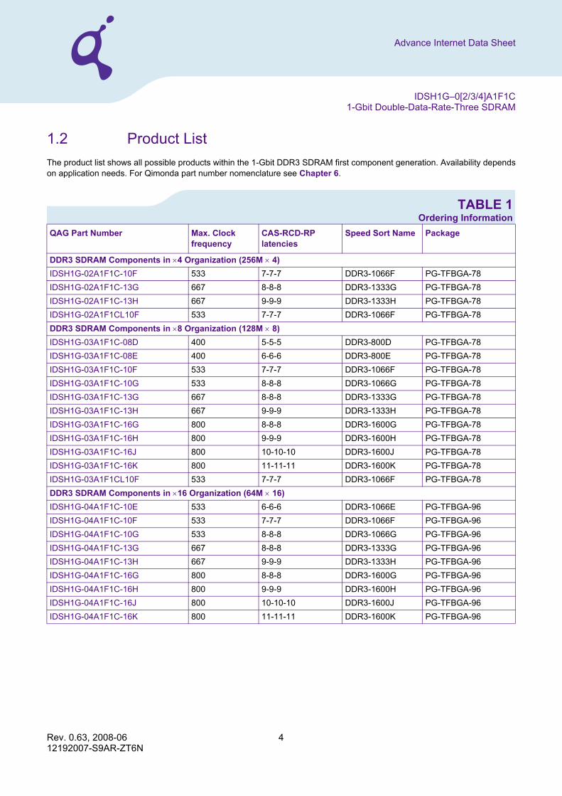
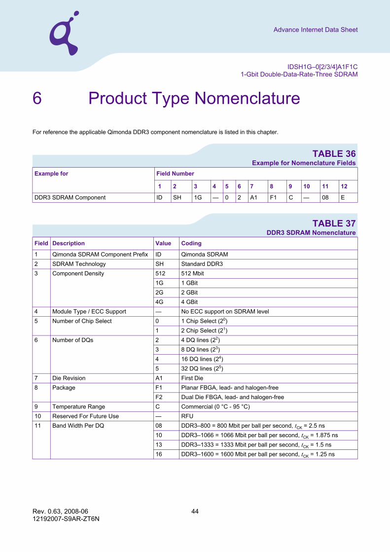
1.2 Product ListThe product list shows all possible products within the 1-Gbit DDR3 SDRAM first component generation. Availability dependson application needs. For Qimonda part number nomenclature see Chapter 6.
TABLE 1Ordering Information
QAG Part Number Max. Clock frequency
CAS-RCD-RP latencies
Speed Sort Name Package
DDR3 SDRAM Components in ×4 Organization (256M × 4)IDSH1G-02A1F1C-10F 533 7-7-7 DDR3-1066F PG-TFBGA-78IDSH1G-02A1F1C-13G 667 8-8-8 DDR3-1333G PG-TFBGA-78IDSH1G-02A1F1C-13H 667 9-9-9 DDR3-1333H PG-TFBGA-78IDSH1G-02A1F1CL10F 533 7-7-7 DDR3-1066F PG-TFBGA-78DDR3 SDRAM Components in ×8 Organization (128M × 8)IDSH1G-03A1F1C-08D 400 5-5-5 DDR3-800D PG-TFBGA-78IDSH1G-03A1F1C-08E 400 6-6-6 DDR3-800E PG-TFBGA-78IDSH1G-03A1F1C-10F 533 7-7-7 DDR3-1066F PG-TFBGA-78IDSH1G-03A1F1C-10G 533 8-8-8 DDR3-1066G PG-TFBGA-78IDSH1G-03A1F1C-13G 667 8-8-8 DDR3-1333G PG-TFBGA-78IDSH1G-03A1F1C-13H 667 9-9-9 DDR3-1333H PG-TFBGA-78IDSH1G-03A1F1C-16G 800 8-8-8 DDR3-1600G PG-TFBGA-78IDSH1G-03A1F1C-16H 800 9-9-9 DDR3-1600H PG-TFBGA-78IDSH1G-03A1F1C-16J 800 10-10-10 DDR3-1600J PG-TFBGA-78IDSH1G-03A1F1C-16K 800 11-11-11 DDR3-1600K PG-TFBGA-78IDSH1G-03A1F1CL10F 533 7-7-7 DDR3-1066F PG-TFBGA-78DDR3 SDRAM Components in ×16 Organization (64M × 16)IDSH1G-04A1F1C-10E 533 6-6-6 DDR3-1066E PG-TFBGA-96IDSH1G-04A1F1C-10F 533 7-7-7 DDR3-1066F PG-TFBGA-96IDSH1G-04A1F1C-10G 533 8-8-8 DDR3-1066G PG-TFBGA-96IDSH1G-04A1F1C-13G 667 8-8-8 DDR3-1333G PG-TFBGA-96IDSH1G-04A1F1C-13H 667 9-9-9 DDR3-1333H PG-TFBGA-96IDSH1G-04A1F1C-16G 800 8-8-8 DDR3-1600G PG-TFBGA-96IDSH1G-04A1F1C-16H 800 9-9-9 DDR3-1600H PG-TFBGA-96IDSH1G-04A1F1C-16J 800 10-10-10 DDR3-1600J PG-TFBGA-96IDSH1G-04A1F1C-16K 800 11-11-11 DDR3-1600K PG-TFBGA-96
Rev. 0.63, 2008-06 412192007-S9AR-ZT6N
IDSH1G–0[2/3/4]A1F1C1-Gbit Double-Data-Rate-Three SDRAM
Advance Internet Data Sheet
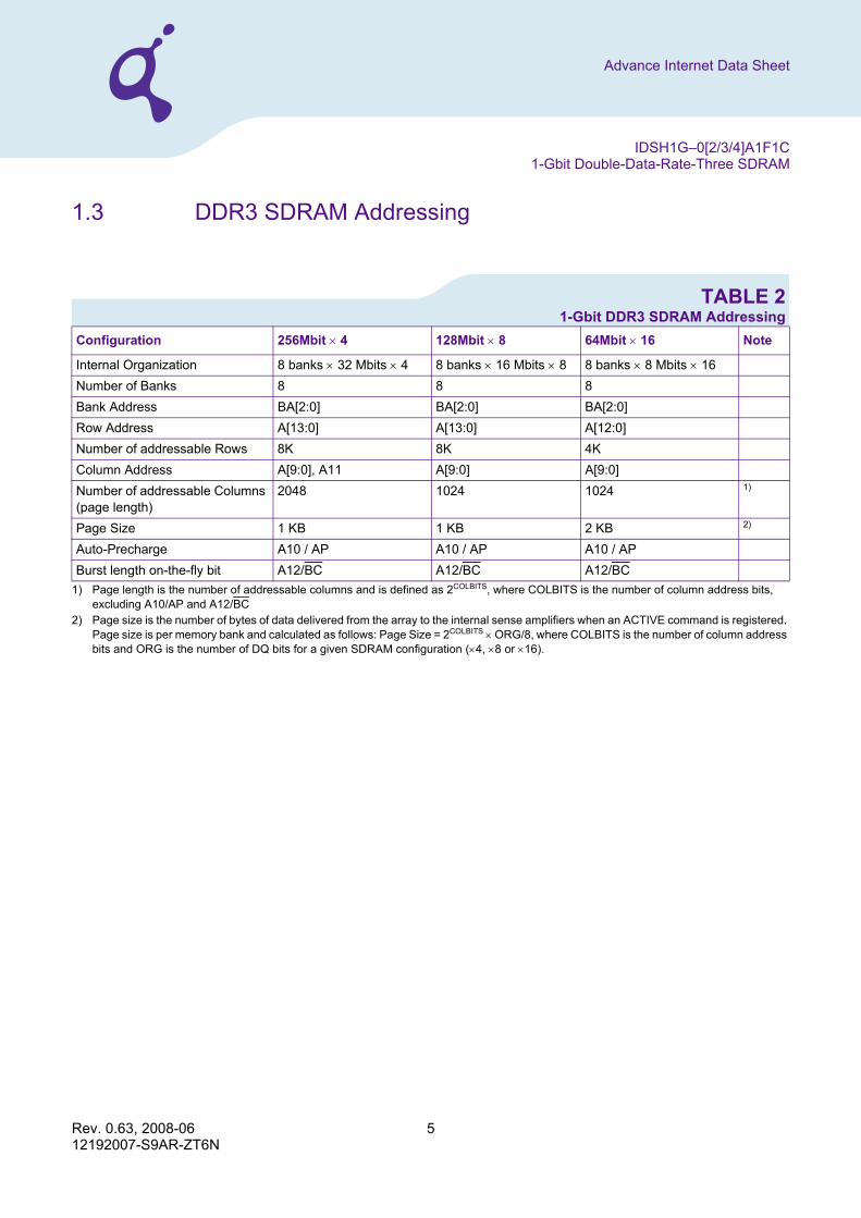
1.3 DDR3 SDRAM Addressing
TABLE 21-Gbit DDR3 SDRAM Addressing
Configuration 256Mbit × 4 128Mbit × 8 64Mbit × 16 Note
Internal Organization 8 banks × 32 Mbits × 4 8 banks × 16 Mbits × 8 8 banks × 8 Mbits × 16Number of Banks 8 8 8Bank Address BA[2:0] BA[2:0] BA[2:0]Row Address A[13:0] A[13:0] A[12:0]Number of addressable Rows 8K 8K 4KColumn Address A[9:0], A11 A[9:0] A[9:0]Number of addressable Columns (page length)
2048 1024 1024 1)
1) Page length is the number of addressable columns and is defined as 2COLBITS, where COLBITS is the number of column address bits, excluding A10/AP and A12/BC
Page Size 1 KB 1 KB 2 KB 2)
2) Page size is the number of bytes of data delivered from the array to the internal sense amplifiers when an ACTIVE command is registered. Page size is per memory bank and calculated as follows: Page Size = 2COLBITS × ORG/8, where COLBITS is the number of column address bits and ORG is the number of DQ bits for a given SDRAM configuration (×4, ×8 or ×16).
Auto-Precharge A10 / AP A10 / AP A10 / APBurst length on-the-fly bit A12/BC A12/BC A12/BC
Rev. 0.63, 2008-06 512192007-S9AR-ZT6N

IDSH1G–0[2/3/4]A1F1C1-Gbit Double-Data-Rate-Three SDRAM
Advance Internet Data Sheet
1.4 Package BalloutFigure 1, Figure 2 and Figure 3 show the ballouts for DDR3 SDRAM components. See Chapter 5 for package outlines.
FIGURE 1Ballout for 1Gb ×4 Components (PG-TFBGA-78)
Rev. 0.63, 2008-06 612192007-S9AR-ZT6N

IDSH1G–0[2/3/4]A1F1C1-Gbit Double-Data-Rate-Three SDRAM
Advance Internet Data Sheet
FIGURE 2Ballout for 1Gb × 8 Components (PG-TFBGA-78)
Rev. 0.63, 2008-06 712192007-S9AR-ZT6N

IDSH1G–0[2/3/4]A1F1C1-Gbit Double-Data-Rate-Three SDRAM
Advance Internet Data Sheet
FIGURE 3Ballout for 1Gb × 16 Components (PG-TFBGA-96)
Rev. 0.63, 2008-06 812192007-S9AR-ZT6N

IDSH1G–0[2/3/4]A1F1C1-Gbit Double-Data-Rate-Three SDRAM
Advance Internet Data Sheet
1.5 Input / Output Signal Functional Description
TABLE 3Input / Output Signal Functional Description
Symbol EDA Signal Name1) Type Function
CK, CK ck_t, ck_c Input Clock: CK and CK are differential clock inputs. All address and control input signals are sampled on the crossing of the positive edge of CK and negative edge of CK.
CKE cke Input Clock Enable: CKE High activates, and CKE Low deactivates internal clock signals and device input buffers and output drivers. Taking CKE Low provides Precharge Power-Down and Self-Refresh operation (all banks idle), or Active Power-Down ( active row in any bank). CKE is asynchronous for Self-Refresh exit. After VREFCA and VREFDQ have become stable during the power on and initialization sequence, they must be maintained during all operations (including Self-Refresh). CKE must be maintained High throughout read and write accesses. Input buffers, excluding CK, CK, ODT, CKE and RESET are disabled during Power-down. Input buffers, excluding CKE and RESET are disabled during self refresh.
CS cs_n Input Chip Select: All command are masked when CS is registered High. CS provides for external Rank selection on systems with multiple ranks. CS is considered part of the command code.
RAS, CAS, WE ras_n, cas_n, we_n Input Command Inputs: RAS, CAS and WE (along with CS) define the command being entered.
ODT odt Input On-Die Termination: ODT (registered High) enables termination resistance internal to the DDR3 SDRAM. When enabled, ODT is only applied to each DQ, DQS, DQS and DM signal for ×4/×8 configurations. For ×16 configuration ODT is applied to each DQ, DQSU, DQSU, DQSL, DQSL, DMU and DML signal. The ODT signal will be ignored if the Mode Register MR1 is programmed to disable ODT and during Self Refresh.
DM (×4, ×8); DMU, DML (×16)
dm (×4); dm_tdqs_t (×8); dmu, dml (×16)
Input Input Data Mask: DM is an input mask signal for write data. Input data is masked when DM is sampled High coincident with that input data during a Write access. DM is sampled on both edges of DQS. DMU and DML are the input mask signals for ×16 components and control the lower or upper bytes.
TDQS/TDQS dm_tdqs_t, nu_tdqs_c
Termination
Termination Data Strobe: TDQS/TDQS is applicable for ×8 DRAMs only. When enabled via Mode Register A11 = 1 in MR1, the DRAM will enable the same termination resistance function on TDQS/TDQS that is applied to DQS/DQS. When disabled via mode register A11 = 0 in MR1, DM/TDQS will provide the data mask function and TDQS is not used. ×4/×16 DRAMs must disable the TDQS function via mode register A11 = 0 in MR1.
BA0 - BA2 ba0 - ba2 Input Bank Address Inputs: Define to which bank an Active, Read, Write or Precharge command is being applied. Bank address also determines which mode register is to be accessed during a mode register set cycle.
Rev. 0.63, 2008-06 912192007-S9AR-ZT6N

IDSH1G–0[2/3/4]A1F1C1-Gbit Double-Data-Rate-Three SDRAM
Advance Internet Data Sheet
Note: Input only pins (BA0-BA2, A0-A15, RAS, CAS, WE, CS, CKE, ODT, and RESET) do not supply termination.
A0 - A13(×4, ×8); A0-A12(×16)
a0 - a13(×4, ×8); a0-a12(×16)
Input Address Inputs: Provides the row address for Active commands and the column address for Read/Write commands to select one location out of the memory array in the respective bank. (A10/AP and A12/BC have additional functions, see below). The address inputs also provide the op-code during Mode Register Set commands. For numbers of addresses used on this assembly see Table 2.
A10 / AP a10 Input Auto-Precharge: A10/AP is sampled during Read/Write commands to determine whether Auto-Precharge should be performed to the accessed bank after the Read/Write operation. (High: Auto-Precharge, Low: no Auto-Precharge). A10/AP is sampled during Precharge command to determine whether the Precharge applies to one bank (A10 Low) or all banks (A10 High). If only one bank is to be precharged, the bank is selected by bank addresses.
A12 / BC a12 Input Burst Chop: A12/BC is sampled during Read and Write commands to determine if burst chop (on-the-fly) will be performed. (High: no burst chop, Low: burst chopped). See “Command Truth Table” on Page 11 for details.
DQ (×4, ×8); DQL/DQU (×16)
dq (×4, ×8)dql/dqu (×16)
Input/Output
Data Input/Output: Bi-directional data bus.
DQS / DQS (×4, ×8);DQSL, DQSL, DQSU, DQSU(×16)
dqs_t / dqs_c (×4, ×8);dqsl_t, dqsl_c, dqsu_t, dqsu_c (×16)
Input/Output
Data Strobe: output with read data, input with write data. Edge-aligned with read data, centered in write data. For the ×16, DQSL corresponds to the data on DQL0 - DQL7; DQSU corresponds to the data on DQU0-DQU7.The data strobes DQS, DQSL and DQSU are paired with differential signals DQS, DQSL and DQSU, respectively, to provide differential pair signaling to the system during both reads and writes. DDR3 SDRAM supports differential data strobe only and does not support single-ended.
RESET reset_n CMOSInput
Active Low Asynchronous Reset: Reset is active when RESET is Low, and inactive when RESET is High. RESET must be High during normal operation. RESET is a CMOS rail to rail signal with DC High and Low are 80% and 20% of VDD, RESET active is destructive to data contents.
NC — — No Connect: no internal electrical connection is presentVDDQ vddq Supply DQ Power Supply: 1.5 V ± 0.075 VVSSQ vssq Supply DQ GroundVDD vdd Supply Power Supply: 1.5 V ± 0.075 VVSS vss Supply GroundVREFDQ vrefdq Supply Reference Voltage for DQVREFCA vrefca Supply Reference Voltage for Command and Address inputsZQ zq Supply Reference ball for ZQ calibration
1) The EDA Signal Name is used in Qimonda's Simulation Models such as IBIS, Verilog, etc.
Symbol EDA Signal Name1) Type Function
Rev. 0.63, 2008-06 1012192007-S9AR-ZT6N
IDSH1G–0[2/3/4]A1F1C1-Gbit Double-Data-Rate-Three SDRAM
Advance Internet Data Sheet
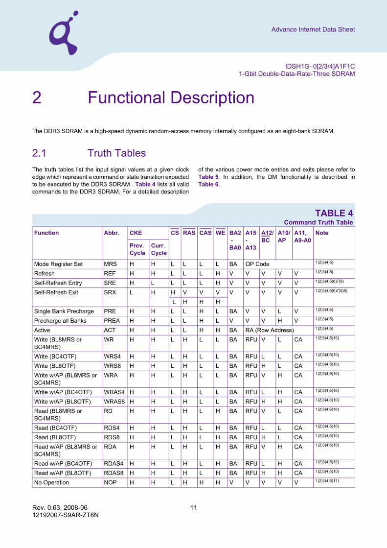
2 Functional Description
The DDR3 SDRAM is a high-speed dynamic random-access memory internally configured as an eight-bank SDRAM.
2.1 Truth TablesThe truth tables list the input signal values at a given clockedge which represent a command or state transition expectedto be executed by the DDR3 SDRAM . Table 4 lists all validcommands to the DDR3 SDRAM. For a detailed description
of the various power mode entries and exits please refer toTable 5. In addition, the DM functionality is described inTable 6.
TABLE 4Command Truth Table
Function Abbr. CKE CS RAS CAS WE BA2-BA0
A15-A13
A12/BC
A10/AP
A11,A9-A0
Note
Prev.Cycle
Curr.Cycle
Mode Register Set MRS H H L L L L BA OP Code 1)2)3)4)5)
Refresh REF H H L L L H V V V V V 1)2)3)4)5)
Self-Refresh Entry SRE H L L L L H V V V V V 1)2)3)4)5)6)7)8)
Self-Refresh Exit SRX L H H V V V V V V V V 1)2)3)4)5)6)7)8)9)
L H H HSingle Bank Precharge PRE H H L L H L BA V V L V 1)2)3)4)5)
Precharge all Banks PREA H H L L H L V V V H V 1)2)3)4)5)
Active ACT H H L L H H BA RA (Row Address) 1)2)3)4)5)
Write (BL8MRS or BC4MRS)
WR H H L H L L BA RFU V L CA 1)2)3)4)5)10)
Write (BC4OTF) WRS4 H H L H L L BA RFU L L CA 1)2)3)4)5)10)
Write (BL8OTF) WRS8 H H L H L L BA RFU H L CA 1)2)3)4)5)10)
Write w/AP (BL8MRS or BC4MRS)
WRA H H L H L L BA RFU V H CA 1)2)3)4)5)10)
Write w/AP (BC4OTF) WRAS4 H H L H L L BA RFU L H CA 1)2)3)4)5)10)
Write w/AP (BL8OTF) WRAS8 H H L H L L BA RFU H H CA 1)2)3)4)5)10)
Read (BL8MRS or BC4MRS)
RD H H L H L H BA RFU V L CA 1)2)3)4)5)10)
Read (BC4OTF) RDS4 H H L H L H BA RFU L L CA 1)2)3)4)5)10)
Read (BL8OTF) RDS8 H H L H L H BA RFU H L CA 1)2)3)4)5)10)
Read w/AP (BL8MRS or BC4MRS)
RDA H H L H L H BA RFU V H CA 1)2)3)4)5)10)
Read w/AP (BC4OTF) RDAS4 H H L H L H BA RFU L H CA 1)2)3)4)5)10)
Read w/AP (BL8OTF) RDAS8 H H L H L H BA RFU H H CA 1)2)3)4)5)10)
No Operation NOP H H L H H H V V V V V 1)2)3)4)5)11)
Rev. 0.63, 2008-06 1112192007-S9AR-ZT6N

IDSH1G–0[2/3/4]A1F1C1-Gbit Double-Data-Rate-Three SDRAM
Advance Internet Data Sheet
Device Deselect DES H H H X X X X X X X X 1)2)3)4)5)12)
Power Down Entry PDE H L L H H H V V V V V 1)2)3)4)5)8)13)
H V V VPower Down Exit PDX L H L H H H V V V V V 1)2)3)4)5)8)13)
H V V VZQ Calibration Short ZQCS H H L H H L X X X L X 1)2)3)4)5)
ZQ Calibration Long ZQCL H H L H H L X X X H X 1)2)3)4)5)
1) BA = Bank Address, RA = Row Address, CA = Column Address, BC = Burst Chop, AP = Auto Precharge, X = Don’t care, V = valid2) All DDR3 SDRAM commands are defined by states of CS, RAS, CAS, WE and CKE at the rising edge of the clock. The higher order
address bits of BA, RA and CA are device density and IO configuration (×4, ×8, ×16) dependent.3) RESET is a low active signal which will be used only for asynchronous reset. It must be maintained High during any function.4) Bank addresses (BA) determine which bank is to be operated upon. For MRS, BA selects a Mode Register.5) V means H or L (but a defined logic level) and X means either “defined or undefined (like floating) logic level”.6) The state of ODT does not affect the states described in this table. The ODT function is not available during Self Refresh7) VREF (both VREFCA and VREFDQ) must be maintained during Self Refresh operation.8) Refer to “Clock Enable (CKE) Truth Table for Synchronous Transitions” on Page 13 for more detail with CKE transition.9) Self refresh exit is asynchronous.10) Burst reads or writes cannot be terminated or interrupted and Fixed/on-the-Fly BL will be defined by MRS.11) The No Operation (NOP) command should be used in cases when the DDR3 SDRAM is in an idle or a wait state. The purpose of the NOP
command is to prevent the DDR3 SDRAM from registering any unwanted commands between operations. A NOP command will not terminate a previous operation that is still executing, such as a read or write burst.
12) The Deselect command (DES) performs the same function as a No Operation command.13) The Power Down Mode does not perform any refresh operation.
Function Abbr. CKE CS RAS CAS WE BA2-BA0
A15-A13
A12/BC
A10/AP
A11,A9-A0
Note
Prev.Cycle
Curr.Cycle
Rev. 0.63, 2008-06 1212192007-S9AR-ZT6N

IDSH1G–0[2/3/4]A1F1C1-Gbit Double-Data-Rate-Three SDRAM
Advance Internet Data Sheet
TABLE 5Clock Enable (CKE) Truth Table for Synchronous Transitions
Current State 1)
1) Current state is defined as the state of the DDR3 SDRAM immediately prior to clock edge N.
CKE(N-1)2)
2) CKE(N) is the logic state of CKE at clock edge N; CKE (N-1) was the state of CKE at the previous clock edge.
CKE(N)2) Command (N)3)RAS, CAS, WE, CS
3) COMMAND (N) is the command registered at clock edge N, and ACTION (N) is a result of COMMAND (N),ODT is not included here.
Action (N)3) Note
PreviousCycle
CurrentCycle
Power Down L L X Maintain Power Down 4)5)6)7)8)9)
4) All states and sequences not shown are illegal or reserved unless explicitly described elsewhere in this document.5) The state of ODT does not affect the states described in this table. The ODT function is not available during Self Refresh.6) CKE must be registered with the same value on tCKE.MIN consecutive positive clock edges. CKE must remain at the valid input level the
entire time it takes to achieve the tCKE.MIN clocks of registeration. Thus, after any CKE transition, CKE may not transition from its valid level during the time period of tIS + tCKE.MIN + tIH.
7) DES and NOP are defined in “Command Truth Table” on Page 11.8) The Power Down does not perform any refresh operations9) X means Don’t care (including floating around VREFCA) in Self Refresh and Power Down. It also applies to address pins.
L H DES or NOP Power Down Exit 4)5)6)7)8)10)
10) Valid commands for Power Down Entry and Exit are NOP and DES only
Self Refresh L L X Maintain Self Refresh 4)5)6)7)9)11)
11) VREF (both VREFCA and VREFDQ) must be maintained during Self Refresh operation.
L H DES or NOP Self Refresh Exit 4)5)6)7)11)12)13)
12) On Self Refresh Exit DES or NOP commands must be issued on every clock edge occurring during the tXS period. Read, or ODT commands may be issued only after tXSDLL is satisfied.
13) Valid commands for Self Refresh Exit are NOP and DES only.
Bank(s) Active H L DES or NOP Active Power Down Entry 4)5)6)7)8)10)14)
14) Self Refresh can not be entered while Read or Write operations are in progress.
Reading H L DES or NOP Power Down Entry 4)5)6)7)8)10)14)15)
15) If all banks are closed at the conclusion of a read, write or precharge command then Precharge Power-down is entered, otherwise Active Power-down is entered.
Writing H L DES or NOP Power Down Entry 4)5)6)7)8)10)14)15)
Precharging H L DES or NOP Power Down Entry 4)5)6)7)8)10)14)15)
Refreshing H L DES or NOP Precharge Power Down Entry 4)5)6)7)10)
All Banks Idle H L DES or NOP Precharge Power Down Entry 4)5)6)7)10)8)14)16)
16) ‘Idle state’ is defined as all banks are closed (tRP, tDAL, etc. satisfied), no data bursts are in progress, CKE is High, and all timings from previous operations are satisfied (tMRD, tMOD, tRFC, tZQ.INIT, tZQ.OPER, tZQCS, etc.) as well as all Self-Refresh exit and Power-Down Exit parameters are satisfied (tXS, tXP, tXPDLL, etc.).
H L REF Self Refresh Entry 4)5)6)7)14)16)17)
17) Self Refresh mode can only be entered from the All Banks Idle state.
Any other state Refer to “Command Truth Table” on Page 11 for more detail with all command signals 4)5)6)7)18)
18) Must be a legal command as defined in “Command Truth Table” on Page 11.
Rev. 0.63, 2008-06 1312192007-S9AR-ZT6N

IDSH1G–0[2/3/4]A1F1C1-Gbit Double-Data-Rate-Three SDRAM
Advance Internet Data Sheet
TABLE 6Data Mask (DM) Truth Table
Name (Function) DM DQs
Write Enable L ValidWrite Inhibit H X
Rev. 0.63, 2008-06 1412192007-S9AR-ZT6N

IDSH1G–0[2/3/4]A1F1C1-Gbit Double-Data-Rate-Three SDRAM
Advance Internet Data Sheet
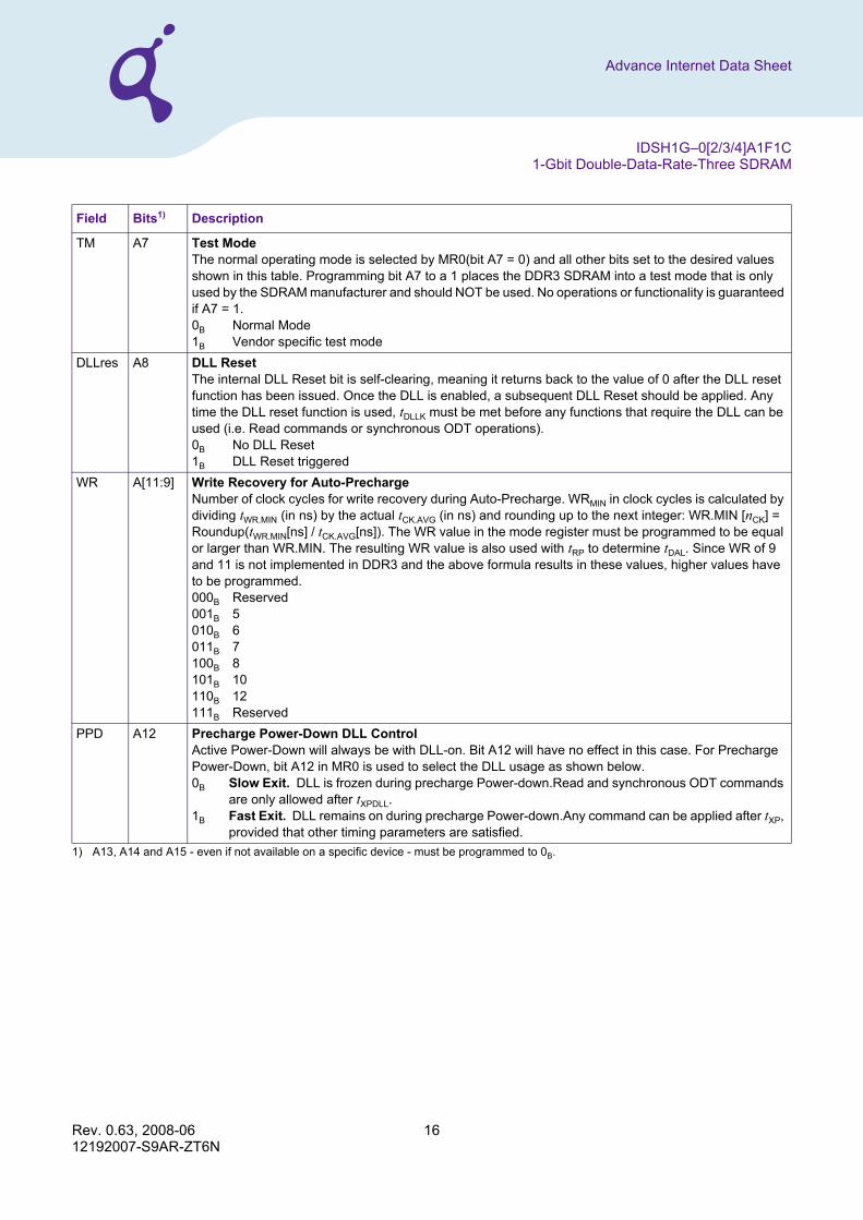
2.2 Mode Register 0 (MR0)The mode register MR0 stores the data for controlling variousoperating modes of DDR3 SDRAM. It controls burst length,read burst type, CAS latency, test mode, DLL reset, WR(write recovery time for auto-precharge) and DLL control forprecharge Power-Down, which includes various vendor
specific options to make DDR3 SDRAM useful for variousapplications. The mode register is written by asserting Low onCS, RAS, CAS, WE, BA0, BA1, and BA2, while controlling thestates of address pins according to Table 7.
TABLE 7MR0 Mode register Definition (BA[2:0]=000B)
Field Bits1) Description
BL A[1:0] Burst Length (BL) and Control MethodNumber of sequential bits per DQ related to one Read/Write command. 00B BL8MRS mode with fixed burst length of 8. A12/BC at Read or Write command time is Don’t care
at read or write command time.01B BLOTF on-the-fly (OTF) enabled using A12/BC at Read or Write command time. When A12/BC is
High during Read or Write command time a burst length of 8 is selected (BL8OTF mode). When A12/BC is Low, a burst chop of 4 is selected (BC4OTF mode). Auto-Precharge can be enabled or disabled.
10B BC4MRS mode with fixed burst chop of 4 with tCCD = 4 × nCK. A12/BC is Don’t care at Read or Write command time.
11B TBD ReservedRBT A3 Read Burst Type
0B Nibble Sequential1B Interleaved
CL A[6:4,2] CAS Latency (CL)CAS Latency is the delay, in clock cycles, between the internal Read command and the availability of the first bit of output data.Note: All other bit combinations are reserved.
0000B RESERVED0010B 50100B 60110B 71000B 81010B 91100B 101110B 11
Rev. 0.63, 2008-06 1512192007-S9AR-ZT6N
IDSH1G–0[2/3/4]A1F1C1-Gbit Double-Data-Rate-Three SDRAM
Advance Internet Data Sheet
TM A7 Test ModeThe normal operating mode is selected by MR0(bit A7 = 0) and all other bits set to the desired values shown in this table. Programming bit A7 to a 1 places the DDR3 SDRAM into a test mode that is only used by the SDRAM manufacturer and should NOT be used. No operations or functionality is guaranteed if A7 = 1.0B Normal Mode1B Vendor specific test mode
DLLres A8 DLL ResetThe internal DLL Reset bit is self-clearing, meaning it returns back to the value of 0 after the DLL reset function has been issued. Once the DLL is enabled, a subsequent DLL Reset should be applied. Any time the DLL reset function is used, tDLLK must be met before any functions that require the DLL can be used (i.e. Read commands or synchronous ODT operations).0B No DLL Reset1B DLL Reset triggered
WR A[11:9] Write Recovery for Auto-PrechargeNumber of clock cycles for write recovery during Auto-Precharge. WRMIN in clock cycles is calculated by dividing tWR.MIN (in ns) by the actual tCK.AVG (in ns) and rounding up to the next integer: WR.MIN [nCK] = Roundup(tWR.MIN[ns] / tCK.AVG[ns]). The WR value in the mode register must be programmed to be equal or larger than WR.MIN. The resulting WR value is also used with tRP to determine tDAL. Since WR of 9 and 11 is not implemented in DDR3 and the above formula results in these values, higher values have to be programmed.000B Reserved001B 5010B 6011B 7100B 8101B 10110B 12111B Reserved
PPD A12 Precharge Power-Down DLL ControlActive Power-Down will always be with DLL-on. Bit A12 will have no effect in this case. For Precharge Power-Down, bit A12 in MR0 is used to select the DLL usage as shown below. 0B Slow Exit. DLL is frozen during precharge Power-down.Read and synchronous ODT commands
are only allowed after tXPDLL.1B Fast Exit. DLL remains on during precharge Power-down.Any command can be applied after tXP,
provided that other timing parameters are satisfied.1) A13, A14 and A15 - even if not available on a specific device - must be programmed to 0B.
Field Bits1) Description
Rev. 0.63, 2008-06 1612192007-S9AR-ZT6N

IDSH1G–0[2/3/4]A1F1C1-Gbit Double-Data-Rate-Three SDRAM
Advance Internet Data Sheet
2.3 Mode Register 1 (MR1)The Mode Register MR1 stores the data for enabling ordisabling the DLL, output driver strength, RTT_NOM impedance,additive latency (AL), Write leveling enable and Qoff (outputdisable). The Mode Register MR1 is written by asserting Low
on CS, RAS, CAS, WE, High on BA0 and Low on BA1andBA2, while controlling the states of address pins according toTable 8.
TABLE 8MR1 Mode Register Definition (BA[2:0]=001B)
Field Bits1) Description
DLLdis A0 DLL DisableThe DLL must be enabled for normal operation. DLL enable is required during power up initialization, after reset and upon returning to normal operation after having the DLL disabled. During normal operation (DLL-on) with MR1(A0 = 0), the DLL is automatically disabled when entering Self-Refresh operation and is automatically re-enabled and reset upon exit of Self-Refresh operation. Any time the DLL is enabled, a DLL reset must be issued afterwards. Any time the DLL is reset, tDLLK clock cycles must occur before a Read or synchronous ODT command can be issued to allow time for the internal clock to be synchronized with the external clock. Failing to wait for synchronization to occur may result in a violation of the tDQSCK, tAON, tAOF or tADC parameters. During tDLLK, CKE must continuously be registered high. DDR3 SDRAM does not require DLL for any Write operation. .0B DLL is enabled1B DLL is disabled
DIC A[5, 1] Output Driver Impedance ControlNote: All other bit combinations are reserved.
00B Nominal Drive Strength RON40 = RZQ/6 (nominal 40.0 Ω, with nominal RZQ = 240 Ω)01B Nominal Drive Strength RON34 = RZQ/7 (nominal 34.3 Ω, with nominal RZQ = 240 Ω)
RTT_NOM A[9, 6, 2] Nominal Termination Resistance of ODT
Notes
1. If RTT_NOM is used during Writes, only the values RZQ/2, RZQ/4 and RZQ/6 are allowed.2. In Write leveling Mode (MR1[bit7] = 1) with MR1[bit12] = 1, all RTT_Nom settings are allowed; in
Write Leveling Mode (MR1[bit7] = 1) with MR1[bit12] = 0, only RTT_NOM settings of RZQ/2, RZQ/4 and RZQ/6 are allowed.
3. All other bit combinations are reserved.000B ODT disabled, RTT_NOM = off, Dynamic ODT mode disabled001B RTT60 = RZQ / 4 (nominal 60 Ω with nominal RZQ = 240 Ω)010B RTT120 = RZQ / 2 (nominal 120 Ω with nominal RZQ = 240 Ω011B RTT40 = RZQ / 6 (nominal 40 Ω with nominal RZQ = 240 Ω)100B RTT20 = RZQ / 12 (nominal 20 Ω with nominal RZQ = 240 Ω)101B RTT30 = RZQ / 8 (nominal 30 Ω with nominal RZQ = 240 Ω)
Rev. 0.63, 2008-06 1712192007-S9AR-ZT6N

IDSH1G–0[2/3/4]A1F1C1-Gbit Double-Data-Rate-Three SDRAM
Advance Internet Data Sheet
AL A[4, 3] Additive Latency (AL)Any read or write command is held for the time of Additive Latency (AL) before it is issued as internal read or write command.
Notes
1. AL has a value of CL - 1 or CL - 2 as per the CL value programmed in the MR0 register.00B AL = 0 (AL disabled)01B AL = CL - 110B AL = CL - 211B Reserved
Level A7 Write Leveling Mode0B Write Leveling Mode Disabled, Normal operation mode1B Write Leveling Mode Enabled
TDQS A11 TDQS enable0B Disable1B Enable
Qoff A12 Output DisableUnder normal operation, the SDRAM outputs are enabled during read operation and write leveling for driving data (Qoff bit in the MR1 is set to 0B). When the Qoff bit is set to 1B, the SDRAM outputs (DQ, DQS, DQS, also on upper byte lane in case of ×16) will be disabled - also during write leveling. Disabling the SDRAM outputs allows users to run write leveling on multiple ranks and to measure IDD currents during Read operations, without including the output.0B Output buffer enabled1B Output buffer disabled
1) A13, A14, A15 - even if not available on a specific device - must be programmed to 0B.
Field Bits1) Description
Rev. 0.63, 2008-06 1812192007-S9AR-ZT6N

IDSH1G–0[2/3/4]A1F1C1-Gbit Double-Data-Rate-Three SDRAM
Advance Internet Data Sheet
2.4 Mode Register 2 (MR2)The Mode Register MR2 stores the data for controllingrefresh related features, RTT_WR impedance, and CAS writelatency. The Mode Register MR2 is written by asserting Low
on CS, RAS, CAS, WE, High on BA1 and Low on BA0 andBA2, while controlling the states of address signals accordingto Table 9.
TABLE 9MR2 Mode Register Definition (BA[2:0]=010B)
Field Bits1) Description
PASR A[2:0] Partial Array Self Refresh (PASR) If PASR (Partial Array Self Refresh) is enabled, data located in areas of the array beyond the specified self refresh location may get lost if self refresh is entered. During non-self-refresh operation, data integrity will be maintained if tREFI conditions are met.000B Full array (Banks 000B - 111B)001B Half Array(Banks 000B - 011B)010B Quarter Array(Banks 000B - 001B)011B 1/8th array (Banks 000B )100B 3/4 array(Banks 010B - 111B)101B Half array(Banks 100B - 111B)110B Quarter array(Banks 110B - 111B)111B 1/8th array(Banks 111B )
CWL A[5:3] CAS Write Latency (CWL)Number of clock cycles from internal write command to first write data in.000B 5 (3.3 ns ≥ tCK.AVG ≥ 2.5 ns)001B 6 (2.5 ns > tCK.AVG ≥ 1.875 ns)010B 7 (1.875 ns > tCK.AVG ≥ 1.5 ns)011B 8 (1.5 ns > tCK.AVG ≥ 1.25 ns)Note: Besides CWL limitations on tCK.AVG, there are also tAA.MIN/MAX restrictions that need to be
observed. For details, please refer to “Speed Bins” on Page 36.ASR A6 Auto Self Refresh (ASR)
When enabled, DDR3 SDRAM will automatically provide appropriate self refresh entry all supported operating temperature values. If not enabled, the SRT bit must be programmed to indicate TOPER during subsequent self refresh operation.0B Disabled, manual Self-Refresh Reference (SRT)1B Auto Self Refresh enabled
Rev. 0.63, 2008-06 1912192007-S9AR-ZT6N

IDSH1G–0[2/3/4]A1F1C1-Gbit Double-Data-Rate-Three SDRAM
Advance Internet Data Sheet
SRT A7 Self-Refresh Temperature Range (SRT)If ASR = 0, the SRT bit must be programmed to indicate TOPER during subsequent self refresh operation. If ASR = 1, SRT bit must be set to 0b.0B Normal operating temperature range1B Extended operating temperature range
RTT_WR A[10:9] Dynamic ODT mode and RTT_WR Pre-selection
Notes
1. The RTT_WR value can be applied during writes even when RTT_NOM is disabled. During write leveling, Dynamic ODT is not available.
00B Dynamic ODT mode disabled01B Dynamic ODT mode enabled with RTT_WR = RZQ/4 = 60 Ω10B Dynamic ODT mode enabled with RTT_WR = RZQ/2 = 120Ω
1) A13, A14, A15 - even if not available on a specific device - must be programmed to 0B.
Field Bits1) Description
Rev. 0.63, 2008-06 2012192007-S9AR-ZT6N
IDSH1G–0[2/3/4]A1F1C1-Gbit Double-Data-Rate-Three SDRAM
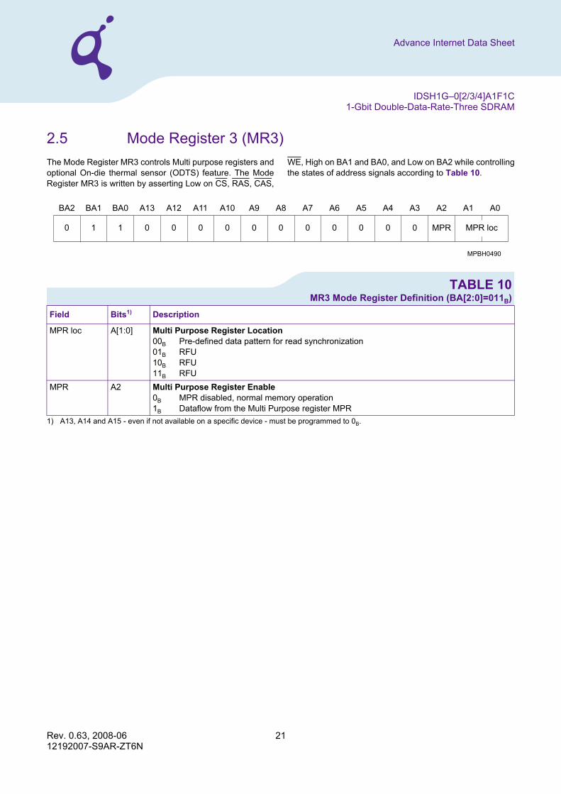
Advance Internet Data Sheet
2.5 Mode Register 3 (MR3)The Mode Register MR3 controls Multi purpose registers andoptional On-die thermal sensor (ODTS) feature. The ModeRegister MR3 is written by asserting Low on CS, RAS, CAS,
WE, High on BA1 and BA0, and Low on BA2 while controllingthe states of address signals according to Table 10.
TABLE 10MR3 Mode Register Definition (BA[2:0]=011B)
Field Bits1)
1) A13, A14 and A15 - even if not available on a specific device - must be programmed to 0B.
Description
MPR loc A[1:0] Multi Purpose Register Location00B Pre-defined data pattern for read synchronization01B RFU10B RFU11B RFU
MPR A2 Multi Purpose Register Enable0B MPR disabled, normal memory operation1B Dataflow from the Multi Purpose register MPR
Rev. 0.63, 2008-06 2112192007-S9AR-ZT6N

IDSH1G–0[2/3/4]A1F1C1-Gbit Double-Data-Rate-Three SDRAM
Advance Internet Data Sheet
2.6 Read / Write Operations and Access ModesAfter a bank has been activated, a read or write access canbe executed. This is accomplished by setting RAS High, CSand CAS Low at the clock’s rising edge. WE must also bedefined at this time to determine whether the access cycle is
a read operation (WE High) or a write operation (WE Low).The DDR3 SDRAM provides a burst column accessoperation. A single Read or Write Command will initiate aserial read or write operation on successive clock edges.
2.6.1 Burst OrderAccesses within a given burst may be interleaved or nibblesequential depending on the programmed bit A3 in the moderegister MR0.Regarding read commands, the lower 3 column address bitsCA[2:0] at read command time determine the start addressfor the read burst.Regarding write commands, the burst order is always fixed.For writes with a burst length of 8, the inputs on the lower 3
column address bits CA[2:0] are ignored during the writecommand. For writes with a burst being chopped to 4, theinput on column address 2 (CA[2]) determines if the lower orupper four burst bits are selected. In this case, the inputs onthe lower 2 column address bits CA[1:0] are ignored duringthe write command.The following table shows burst orderversus burst start address for reads and writes of bursts of 8as well as of bursts of 4 operation (burst chop).
TABLE 11Bit Order during Burst
Burst Length
Command Column Address 2:0
Interleaved Burst Sequence Nibble Sequential Burst Sequence
Note
Bit Order within Burst Bit Order within Burst
CA2 CA1 CA0 1. 2. 3. 4. 5. 6. 7. 8. 1. 2. 3. 4. 5. 6. 7. 8.
8 READ 0 0 0 0 1 2 3 4 5 6 7 0 1 2 3 4 5 6 7 1)
0 0 1 1 0 3 2 5 4 7 6 1 2 3 0 5 6 7 4 1)
0 1 0 2 3 0 1 6 7 4 5 2 3 0 1 6 7 4 5 1)
0 1 1 3 2 1 0 7 6 5 4 3 0 1 2 7 4 5 6 1)
1 0 0 4 5 6 7 0 1 2 3 4 5 6 7 0 1 2 3 1)
1 0 1 5 4 7 6 1 0 3 2 5 6 7 4 1 2 3 0 1)
1 1 0 6 7 4 5 2 3 0 1 6 7 4 5 2 3 0 1 1)
1 1 1 7 6 5 4 3 2 1 0 7 4 5 6 3 0 1 2 1)
WRITE V V V 0 1 2 3 4 5 6 7 0 1 2 3 4 5 6 7 1)2)
4 (Burst Chop Mode)
READ 0 0 0 0 1 2 3 T T T T 0 1 2 3 T T T T 1)3)4)
0 0 1 1 0 3 2 T T T T 1 2 3 0 T T T T 1)3)4)
0 1 0 2 3 0 1 T T T T 2 3 0 1 T T T T 1)3)4)
0 1 1 3 2 1 0 T T T T 3 0 1 2 T T T T 1)3)4)
1 0 0 4 5 6 7 T T T T 4 5 6 7 T T T T 1)3)4)
1 0 1 5 4 7 6 T T T T 5 6 7 4 T T T T 1)3)4)
1 1 0 6 7 4 5 T T T T 6 7 4 5 T T T T 1)3)4)
1 1 1 7 6 5 4 T T T T 7 4 5 6 T T T T 1)3)4)
WRITE 0 V V 0 1 2 3 X X X X 0 1 2 3 X X X X 1)2)4)5)
1 V V 4 5 6 7 X X X X 4 5 6 7 X X X X 1)2)4)5)
Rev. 0.63, 2008-06 2212192007-S9AR-ZT6N

IDSH1G–0[2/3/4]A1F1C1-Gbit Double-Data-Rate-Three SDRAM
Advance Internet Data Sheet
1) 0...7 bit number is value of CA[2:0] that causes this bit to be the first read during a burst.2) V: a valid logic level (0 or 1), but respective buffer input ignores level on input pins.3) T: output drivers for data and strobe are in high impedance.4) In case of BC4MRS (burst length being fixed to 4 by MR0 setting), the internal write operation starts two clock cycles earlier than for the
BL8 modes. This means that the starting point for tWR and tWTR will be pulled in by two clocks. In case of BC4OTF mode (burst length being selected on-the-fly via A12/BC), the internal write operation starts at the same point in time as a burst of 8 write operation. This means that during on-the-fly control, the starting point for tWR and tWTR will not be pulled in by two clocks.
5) X: Don’t Care
Rev. 0.63, 2008-06 2312192007-S9AR-ZT6N

IDSH1G–0[2/3/4]A1F1C1-Gbit Double-Data-Rate-Three SDRAM
Advance Internet Data Sheet
3 Operating Conditions and Interface Specification
3.1 Absolute Maximum Ratings
TABLE 12Absolute Maximum Ratings
Parameter Symbol Rating Unit Note
Min. Max.
Voltage on VDD ball relative to VSS VDD –0.4 +1.975 V 1)2)
1) Stresses greater than those listed under “Absolute Maximum Ratings” may cause permanent damage to the device. This is a stress rating only and functional operation of the device at these or any other conditions above those indicated in the operational sections of this specification is not implied. Exposure to absolute maximum rating conditions for extended periods may affect reliability.
2) VDD and VDDQ must be within 300mV of each other at all times. VREFDQ and VREFCA must not be greater than 0.6 × VDDQ. When VDD and VDDQ are less than 500 mV, VREFDQ and VREFCA may be equal or less than 300 mV.
Voltage on VDDQ ball relative to VSS VDDQ –0.4 +1.975 V 1)2)
Voltage on any ball relative to VSS VIN, VOUT –0.4 +1.975 V 1)
Storage Temperature TSTG –55 +100 °C 1)3)
3) Storage Temperature is the case surface temperature on the center/top side of the SDRAM. For the measurement conditions, please refer to JESD51-2 standard.
Rev. 0.63, 2008-06 2412192007-S9AR-ZT6N

IDSH1G–0[2/3/4]A1F1C1-Gbit Double-Data-Rate-Three SDRAM
Advance Internet Data Sheet
3.2 Operating Conditions
TABLE 13SDRAM Component Operating Temperature Range
TABLE 14DC Operating Conditions
Parameter Symbol Rating Unit Note
Min. Max.
Normal Operating Temperature Range TOPER 0 85 °C 1)2)3)
1) Operating Temperature TOPER is the case surface temperature on the center / top side of the SDRAM. For measurement conditions, please refer to the JEDEC document JESD51-2.
2) The Normal Temperature Range specifies the temperatures where all SDRAM specification will be supported. 3) During operation, the SDRAM operating temperature must be maintained above 0 °C under all operating conditions. Either the device
operating temperature rating may be used to set an appropriate refresh rate and/or to monitor the maximum operating temperature.
Extended Temperature Range 85 95 °C 1)3)4)
4) Some application require operation of the DRAM in the Extended Temperature Range between 85 °C and 95 °C operating temperature. Full specifications are provided in this range, but the following additional conditions apply: a) Refresh commands have to be doubled in frequency, therefore reducing the Refresh interval tREFI to 3.9 µs. b) If Self-Refresh operation is required in the Extended Temperature Range, than it is mandatory to either use the Manual Self-Refresh mode with Extended Temperature Range capability (MR2 A6 = 0B and MR2 A7 = 1B) or enable the Auto Self-Refresh mode (ASR) (MR2 A6 = 1B and MR2 A7= 0B). For SDRAM operations on DIMM module refer to DIMM module data sheets and SPD bytes for Extended Temperature and Auto Self-Refresh option availability.
Parameter Symbol Min. Typ. Max. Unit Note
Supply Voltage VDD 1.425 1.5 1.575 V 1)2)
1) VDDQ tracks with VDD. AC parameters are measured with VDD and VDDQ tied together2) Under all conditions VDDQ must be less than or equal to VDD.
Supply Voltage for Output VDDQ 1.425 1.5 1.575 V 1)2)
Reference Voltage for DQ, DM inputs VREFDQ.DC 0.49 × VDD 0.5 × VDD 0.51 × VDD V 3)4)
3) The AC peak noise on VREF may not allow VREF to deviate from VREF.DC by more than ±1% VDD (for reference: approx. ± 15 mV).4) For reference: approx. VDD/2 ± 15 mV.
Reference Voltage for ADD, CMD inputs VREFCA.DC 0.49 × VDD 0.5 × VDD 0.51 × VDD V 3)4)
External Calibration Resistor connected from ZQ ball to ground RZQ 237.6 240.0 242.4 Ω 5)
5) The external calibration resistor RZQ can be time-shared among DRAMs in multi-rank DIMMs.
Rev. 0.63, 2008-06 2512192007-S9AR-ZT6N
IDSH1G–0[2/3/4]A1F1C1-Gbit Double-Data-Rate-Three SDRAM
Advance Internet Data Sheet
TABLE 15Input and Output Leakage Currents
3.3 Interface Test ConditionsFigure 4 represents the effective reference load of 25 Ω usedin defining the relevant timing parameters of the device aswell as for output slew rate measurements. It is not intendedas either a precise representation of the typical systemenvironment nor a depiction of the actual load presented by a
production tester. System designers should use IBIS or othersimulation tools to correlate the timing reference load to asystem environment. Qimonda correlates to its productiontest conditions, generally one or more coaxial transmissionlines terminated at the tester electronics.
FIGURE 4Reference Load for AC Timings and Output Slew Rates
The Timing Reference Points are the idealized input andoutput nodes / terminals on the outside of the packagedSDRAM device as they would appear in a schematic or anIBIS model. The output timing reference voltage level for
single ended signals is the cross point with VTT. The outputtiming reference voltage level for differential signals is thecross point of the true (e.g. DQS) and the complement (e.g.DQS) signal.
Parameter Symbol Condition Rating Unit Note
Min. Max.
Input Leakage Current IIL Any input 0 V < VIN < VDD –2 +2 µA 1)2)
1) All other balls not under test = 0 V.2) Values are shown per ball.
Output Leakage Current IOL 0V < VOUT < VDDQ –5 +5 µA 2)3)
3) DQ’s, DQS, DQS and ODT are disabled.
Rev. 0.63, 2008-06 2612192007-S9AR-ZT6N

IDSH1G–0[2/3/4]A1F1C1-Gbit Double-Data-Rate-Three SDRAM
Advance Internet Data Sheet
3.4 Voltage Levels
3.4.1 DC and AC Logic Input LevelsTable 16 shows the input levels for single-ended input signals for Address and Control Signals.Table 17 shows the input levels for single-ended input signals for DQ and DM Signals.
TABLE 16DC and AC Input Levels for Single-Ended Command, Address and Control Signals
TABLE 17DC and AC Input Levels for Single-Ended DQ and DM Signals
Parameter Symbol DDR3-800, DDR3-1066 DDR3-1333, DDR3-1600 Unit Note
Min. Max. Min. Max.
DC input logic high VIH.CA.DC VREF + 0.100 VDD VREF + 0.100 VDD V 1)
1) For input only pins except RESET: VREF = VREF.CA
DC input logic low VIL.CA.DC VSS VREF - 0.100 VSS VREF - 0.100 V 1)
AC input logic high VIH.CA.AC VREF + 0.175 See 2)
2) See Chapter 3.9, Overshoot and Undershoot Specification.
VREF + 0.175 See 2) V 1)
AC input logic low VIL.CA.AC See 2) VREF - 0.175 See 2) VREF - 0.175 V 1)
Reduced AC input logic high VIH.CA.AC150 VREF + 0.150 See 2) VREF + 0.150 See 2) V 1)
Reduced AC input logic low VIL.CA.AC150 See 2) VREF - 0.150 See 2) VREF - 0.150 V 1)
Parameter Symbol DDR3-800, DDR3-1066 DDR3-1333, DDR3-1600 Unit Note
Min. Max. Min. Max.
DC input logic high VIH.DQ.DC VREF + 0.100 VDD VREF + 0.100 VDD V 1)
1) For DQ and DM: VREF = VREFDQ, for input only signals except RESET: VREF = VREFCA
DC input logic low VIL.DQ.DC VSS VREF - 0.100 VSS VREF - 0.100 V 1)
AC input logic high VIH.DQ.AC VREF + 0.175 See 2)
2) See Chapter 3.9, Overshoot and Undershoot Specification.
VREF + 0.150 See 2) V 1) 3)
3) Single ended swing requirement for DQS, DQS is 350 mV (peak to peak). Differential swing requirement for DQS, DQS is 700 mV (peak to peak).
AC input logic low VIL.DQ.AC See 2) VREF - 0.175 See 2) VREF - 0.150 V 1) 3)
Rev. 0.63, 2008-06 2712192007-S9AR-ZT6N

IDSH1G–0[2/3/4]A1F1C1-Gbit Double-Data-Rate-Three SDRAM
Advance Internet Data Sheet
Differential Swing Requirement for Differential Signals
Table 18 shows the input levels for differential input signals.
TABLE 18Differential Swing Requirement for Clock (CK - CK) and Strobe (DQS - DQS)
TABLE 19Allowed Time Before Ringback (tDVAC) for CLK - CLK and DQS - DQS
Single-Ended Requirements for Differential Signals
Each individual component of a differential signal (for ×4, ×8:CK, DQS, CK, DQS, for ×16: CK, DQSL, DQSU, CK, DQSL,DQSU) has also to comply with certain requirements forsingle-ended signals. CK and CK have to approximatelyreach VSEH.MIN / VSEL.MAX (approximately equal to the AC-levels (VIH.CA.AC / VIL.CA.AC) for ADD/CMD signals) in everyhalf-cycle. DQS, DQS (×4, ×8) and DQSL, DQSL, DQSU,
DQSU (×16), respectively, have to reach VSEH.MIN / VSEL.MAX(approximately the AC-levels (VIH.DQ.AC / VIL.DQ.AC) for DQsignals) in every half-cycle preceeding and following a validtransition. Note that the applicable AC-levels for ADD/CMDand DQs might be different per speed-bin etc. E.g. ifVIH.CA.AC150 / VIL.CA.AC150 is used for ADD/CMD signals, then
Parameter Symbol DDR3–800, DDR3–1066, DDR3–1333, DDR3–1600 Unit Note
Min. Max.
Differential input high VIH.DIFF +0.200 See 1)
1) These values are not defined, however they single-ended signals CK, CK, DQS, DQS, DQSL, DQSL, DQSU, DQSU need to be within the respective limits ( VIH.DC.MAX , VIL.DC.MIN ) for single-ended signals as well as the limitations for overshoot and undershoot. Refer to Chapter 3.9.
V 2)
2) Used to define a differential signal slew-rate.
Differential input low VIL.DIFF See1) –0.200 V 2)
Differential input high AC VIH.DIFF.AC 2 × (VIH.AC - VREF) 3)
3) Clock: use VIH.CA.AC for VIH.AC. Strobe: use VIH.DQ.AC for VIH.AC.
See 1) V 4)
4) For CK - CK use VIH /VIL.CA.AC of ADD/CMD and VREFCA ; for DQS - DQS (×4, ×8); or DQSL - DQSL, DQSU - DQSU (×16) use VIH /VIL.DQ.AC of DQs and VREFDQ; if a reduced AC-high or AC-low level is used for a signal group, then the reduced level applies also here.
Differential input low AC VIL.DIFF.AC See 1) 2 × (VREF - VIL.AC) 5)
5) Clock: use VIL.CA.AC for VIL.AC. Strobe: use VIL.DQ.AC for VIL.AC.
V 4)
Slew Rate [V/ns] tDVAC [ps] @ |VIH/IL.DIFF.AC| = 350mV
tDVAC [ps]@ |VIH/IL.DIFF.AC| = 300mV
Min. Max. Min. Max.
> 4.0 75 — 175 —4.0 57 — 170 —3.0 50 — 167 —2.0 38 — 163 —1.8 34 — 162 —1.6 29 — 161 —1.4 22 — 159 —1.2 13 — 155 —1.0 0 — 150 —<1.0 0 — 150 —
Rev. 0.63, 2008-06 2812192007-S9AR-ZT6N

IDSH1G–0[2/3/4]A1F1C1-Gbit Double-Data-Rate-Three SDRAM
Advance Internet Data Sheet
these AC-levels apply also for the single-ended signals CKand CK.Note that while ADD/CMD and DQ signal requirements arewith respect to VREF, the single-ended components ofdifferential signals have a requirement with respect to VDD/2;this is nominally the same. The transition of single-ended
signals through the AC-levels is used to measure setup time.For single-ended components of differential signals therequirement to reach VSEL.MAX, VSEH.MIN has no bearing ontiming, but adds a restriction on the common modecharateristics of these signals.
TABLE 20Each Single-Ended Levels for CK, CK, DQS, DQS, DQSL, DQSL, DQSU or DQSU
TABLE 21Cross Point Voltage for Differential Input Signals (CK, DQS)
Parameter Symbol DDR3–800, DDR3–1066, DDR3–1333, DDR3–1600 Unit Note
Min. Max.
Single-ended high-level for strobes VSEH (VDD/2) + 0.175 See 1)
1) These values are not defined, however they single-ended signals CK, CK, DQS, DQS, DQSL, DQSL, DQSU, DQSU need to be within the respective limits ( VIH.DC.MAX , VIL.DC.MIN ) for single-ended signals as well as the limitations for overshoot and undershoot.
V 2)3)
2) For CK, CK use VIH.CA.AC /VIL.CA.AC of ADD/CMD; for strobes (DQS, DQS, DQSL, DQSL, DQSU, DQSU) use VIH.DQ.AC/VIL.DQ.AC of DQs.3) VIH.DQ.AC/VIL.DQ.AC for DQs is based on VREFDQ; VIH.CA.AC/VIL.CA.AC for ADD/CMD is based on VREFCA; if a reduced AC-high or ac-low level is
used for a signal group, then the reduced level applies also here.
Single-ended high-level for CK, CK VSEH (VDD/2) + 0.175 See 1) VSingle-ended low-level for strobes VSEL See 1) (VDD/2) - 0.175 VSingle-ended low-level for CK, CK VSEL See 1) (VDD/2) - 0.175 V
Symbol Parameter DDR3–800, DDR3–1066, DDR3–1333, DDR3–1600
Unit Note
Min. Max.
VIX Differential Input Cross Point Voltage relative to VDD/2 for CK - CK
–150 150 mV–175 175 mV 1)
1) Extended range for VIX is only allowed for clock and if single-ended clock input signals CK and CK are monotonic, have a single-ended swing VSEL/VSEH (see Single-Ended Requirements for Differential Signals) of at least VDD/2 +/-250 mV and if the differential slew rate of CK - CK is larger than 3 V/ns.
VIX Differential Input Cross Point Voltage relative to VDD/2 for DQS -DQS
–150 150 mV
Rev. 0.63, 2008-06 2912192007-S9AR-ZT6N

IDSH1G–0[2/3/4]A1F1C1-Gbit Double-Data-Rate-Three SDRAM
Advance Internet Data Sheet
3.4.2 DC and AC Output Measurements Levels
TABLE 22DC and AC Output Levels for Single-Ended Signals
TABLE 23AC Output Levels for Differential Signals
Parameter Symbol Value Unit Note
DC output high measurement level (for output impedance measurement) VOH.DC 0.8 × VDDQ VDC output mid measurement level (for output impedance measurement) VOM.DC 0.5 × VDDQ VDC output low measurement level (for output impedance measurement) VOL.DC 0.2 × VDDQ VAC output high measurement level (for output slew rate) VOH.AC VTT + 0.1 × VDDQ V 1)
1) Background: the swing of ± 0.1 × VDDQ is based on approximately 50% of the static differential output high or low swing with a driver impedance of 40 Ω and an effective test load of 25 Ω to VTT = VDDQ / 2.
AC output low measurement level (for output slew rate) VOL.AC VTT - 0.1 × VDDQ V 1)
Parameter Symbol Value Unit Note
Min. Max.
AC differential output high measurement level (for output slew rate) VOH.DIFF.AC +0.2 × VDDQ V 1)
1) Background: the swing of ± 0.2 × VDDQ is based on approximately 50% of the static differential output high or low swing with a driver impedance of 40 Ω and an effective test load of 25 Ω to VTT =VDDQ / 2 at each of the differential outputs.
AC differential output low measurement level (for output slew rate) VOL.DIFF.AC –0.2 × VDDQ V 1)
Deviation of the output cross pointvoltage from the termination voltage VOX -100 100 mV 2)
2) With an effective test load of 25 Ω to VTT = VDDQ/2 at each of the differential outputs (see chapter Chapter 3.3, Interface Test Conditions).
Rev. 0.63, 2008-06 3012192007-S9AR-ZT6N

IDSH1G–0[2/3/4]A1F1C1-Gbit Double-Data-Rate-Three SDRAM
Advance Internet Data Sheet
3.5 ODT DC Impedance and Mid-Level CharacteristicsTable 24 provides the ODT DC impedance and mid-level characteristics.
TABLE 24ODT DC Impedance and Mid-Level Characteristics
3.6 ODT DC Impedance Sensitivity on Temperature and Voltage Drifts
If temperature and/or voltage change after calibration, the tolerance limits widen for RTT according to the following tables. Thefollowing definitions are used: ΔT = T - T (at calibration)ΔV = VDDQ- VDDQ (at calibration)VDD = VDDQ
TABLE 25ODT DC Impedance after proper IO Calibration and Voltage/Temperature Drift
Symbol Description VOUT Condition Min. Nom. Max. Unit Note
RTT120 RTT effective = 120 Ω VIL.AC and VIH.AC 0.9 1.0 1.6 RZQ/2 1)2)3)4)
1) With RZQ = 240 Ω.2) Measurement definition for RTT : Apply VIH.AC and VIL.AC to test ball separately, then measure current I (VIH.AC) and I (VIL.AC) respectively.
RTT = [VIH.AC - VIL.AC] / [I (VIH.AC) - I (VIL.AC)]3) The tolerance limits are specified after calibration with stable voltage and temperature. For the behaviour of the tolerance limits if
temperature or voltage changes after calibration, see the ODT DC Impedance Sensitivity on Temperature and Voltage Drifts.4) The tolerance limits are specified under the condition that VDDQ = VDD and that VSSQ = VSS.
RTT60 RTT effective = 60 Ω 0.9 1.0 1.6 RZQ/4 1)2)3)4)
RTT40 RTT effective = 40 Ω 0.9 1.0 1.6 RZQ/6 1)2)3)4)
RTT30 RTT effective = 30 Ω 0.9 1.0 1.6 RZQ/8 1)2)3)4)
RTT20 RTT effective = 20 Ω 0.9 1.0 1.6 RZQ/12 1)2)3)4)
ΔVM Deviation of VM with respect to VDDQ / 2 floating –5 — +5 % 1)2)3)4)5)
5) Measurement Definition for ΔVM: Measure voltage (VM) at test ball (midpoint) with no load: ΔVM = (2 × VM / VDDQ - 1) × 100%
Symbol Value Unit Note
Min. Max.
RTT 0.9 - dRTTdT × |ΔT| - dRTTdV × |ΔV| 1.6 + dRTTdT × |ΔT| + dRTTdV × |ΔV| RZQ / TISFRTT1)
1) TISFRTT: Termination Impedance Scaling Factor for RTT:TISFRTT = 12 for RTT020 TISFRTT = 8 for RTT030 TISFRTT = 6 for RTT040 TISFRTT = 4 for RTT060 TISFRTT = 2 for RTT120
Rev. 0.63, 2008-06 3112192007-S9AR-ZT6N
IDSH1G–0[2/3/4]A1F1C1-Gbit Double-Data-Rate-Three SDRAM
Advance Internet Data Sheet
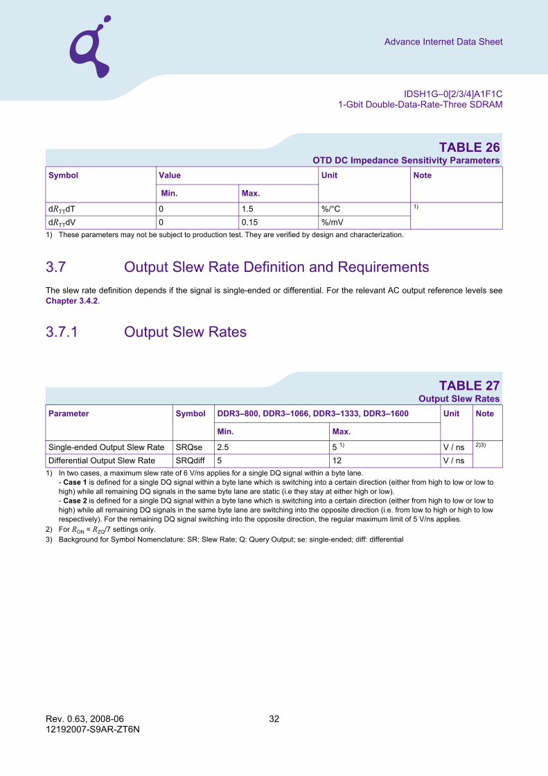
TABLE 26OTD DC Impedance Sensitivity Parameters
3.7 Output Slew Rate Definition and RequirementsThe slew rate definition depends if the signal is single-ended or differential. For the relevant AC output reference levels seeChapter 3.4.2.
3.7.1 Output Slew Rates
TABLE 27Output Slew Rates
Symbol Value Unit Note
Min. Max.
dRTTdT 0 1.5 %/°C 1)
1) These parameters may not be subject to production test. They are verified by design and characterization.dRTTdV 0 0.15 %/mV
Parameter Symbol DDR3–800, DDR3–1066, DDR3–1333, DDR3–1600 Unit Note
Min. Max.
Single-ended Output Slew Rate SRQse 2.5 5 1)
1) In two cases, a maximum slew rate of 6 V/ns applies for a single DQ signal within a byte lane. - Case 1 is defined for a single DQ signal within a byte lane which is switching into a certain direction (either from high to low or low to high) while all remaining DQ signals in the same byte lane are static (i.e they stay at either high or low).- Case 2 is defined for a single DQ signal within a byte lane which is switching into a certain direction (either from high to low or low to high) while all remaining DQ signals in the same byte lane are switching into the opposite direction (i.e. from low to high or high to low respectively). For the remaining DQ signal switching into the opposite direction, the regular maximum limit of 5 V/ns applies.
V / ns 2)3)
2) For RON = RZQ/7 settings only.3) Background for Symbol Nomenclature: SR: Slew Rate; Q: Query Output; se: single-ended; diff: differential
Differential Output Slew Rate SRQdiff 5 12 V / ns
Rev. 0.63, 2008-06 3212192007-S9AR-ZT6N

IDSH1G–0[2/3/4]A1F1C1-Gbit Double-Data-Rate-Three SDRAM
Advance Internet Data Sheet
3.8 Interface CapacitanceDefinition and values for interface capacitances are provided in the following table.
TABLE 28Interface Capacitance Values
Parameter Signals Symbol DDR3–800 DDR3–1066 DDR3–1333 DDR3–1600 Unit Note
Min. Max. Min. Max. Min. Max. Min. Max.
Input/Output Capacitance
DQ, DM, DQS, DQS
CIO 1.5 3.0 1.5 2.7 1.5 2.5 1.5 2.3 pF 1)2)3)
1) Although the DM signal has different function, the loading matches DQ and DQS2) This parameter is not subject to production test. It is verified by design and characterization. Capacitance is measured according to JEP147
(Procedure for measuring input capacitance using a vector network analyzer (VNA) with VDD, VDDQ, VSS, VSSQ applied and all other balls floating (except the ball under test, CKE, RESET and ODT as necessary). VDD = VDDQ = 1.5 V, VBIAS = VDD/2 and on-die termination off
3) This parameter applies to monolithic devices only; stacked/dual-die devices are not covered here
Input Capacitance CK, CK CCK 0.8 1.6 0.8 1.6 0.8 1.4 0.8 1.4 pF 2)3)
Delta of Input Capacitance
CK, CK CDCK 0 0.15 0 0.15 0 0.15 0 0.15 pF 2)3)4)
4) Absolute value of CCK - CCK#
Delta of Input/Output Capacitance of DQS balls
DQS, DQS CDDQS 0 0.2 0 0.2 0 0.15 0 0.15 pF 2)3)5)
5) Absolute value of CIO.DQS - CIO.DQS#
Input Capacitance All other input-only pins
CI 0.75 1.5 0.75 1.5 0.75 1.3 0.75 1.3 pF 2)3)6)
6) CI applies to ODT, CS, CKE, A[A13:0] (×4, ×8) or A[A12:0] (×16), BA[2:0], RAS, CAS, WE
Delta of Input Capacitance
All CTRL input-only pins
CDI.CTRL –0.5 0.3 –0.5 0.3 –0.4 0.2 –0.4 0.2 pF 2)3)7)8)
7) CDI_CTRL applies to ODT, CS and CKE8) CDI_CTRL = CI.CTRL - 0.5 × (CCK + CCK#)
Delta of Input Capacitance
All ADD and CMD input-only pins
CDI.ADD_CMD –0.5 0.5 –0.5 0.5 –0.4 0.4 –0.4 0.4 pF 2)3)9)
10)
9) CDI_ADD_CMD applies to A[A13:0] (×4, ×8) or A[A12:0] (×16), BA[2:0], BA[2:0], RAS, CAS and WE10) CDI_ADD_CMD = CI.ADD,CMD - 0.5 × (CI.CK + CI.CK#)
Delta of Input/Output Capacitance
DQ, DM, DQS, DQS
CDIO –0.5 0.3 –0.5 0.3 –0.5 0.3 –0.5 0.3 pF 2)3)11)
11) CDIO = CIO.DQ,DM - 0.5 × (CIO.DQS + CIO.DQS#)
ZQ Capacitance ZQ CZQ – 3 – 3 – 3 – 3 pF 12)
12) Maximum external load capacitance on ZQ signal: 5 pF
Rev. 0.63, 2008-06 3312192007-S9AR-ZT6N

IDSH1G–0[2/3/4]A1F1C1-Gbit Double-Data-Rate-Three SDRAM
Advance Internet Data Sheet
3.9 Overshoot and Undershoot Specification
TABLE 29AC Overshoot / Undershoot Specification for Address and Control Signals
FIGURE 5AC Overshoot / Undershoot Definitions for Address and Control Signals
TABLE 30AC Overshoot / Undershoot Specification for Clock, Data, Strobe and Mask Signals
Parameter DDR3–800 DDR3–1066 DDR3–1333 DDR3–1600 Unit Note
Maximum peak amplitude allowed for overshoot area 0.4 0.4 0.4 0.4 V 1)
1) Applies for the following signals: A[15:0], BA[3:0], CS, RAS, CAS, WE, CKE and ODT
Maximum peak amplitude allowed for undershoot area
0.4 0.4 0.4 0.4 V 1)
Maximum overshoot area above VDD 0.67 0.5 0.4 0.33 V × ns 1)
Maximum undershoot area below VSS 0.67 0.5 0.4 0.33 V × ns 1)
Parameter DDR3–800
DDR3–1066
DDR3–1333
DDR3–1600
Unit Note
Maximum peak amplitude allowed for overshoot area 0.4 0.4 0.4 0.4 V 1)
1) Applies for CK, CK, DQ, DQS, DQS & DM
Maximum peak amplitude allowed for undershoot area
0.4 0.4 0.4 0.4 V 1)
Maximum overshoot area above VDDQ 0.25 0.19 0.15 0.13 V × ns 1)
Maximum undershoot area below VSSQ 0.25 0.19 0.15 0.13 V × ns 1)
Rev. 0.63, 2008-06 3412192007-S9AR-ZT6N

IDSH1G–0[2/3/4]A1F1C1-Gbit Double-Data-Rate-Three SDRAM
Advance Internet Data Sheet
FIGURE 6AC Overshoot / Undershoot Definitions for Clock, Data, Strobe and Mask Signals
Rev. 0.63, 2008-06 3512192007-S9AR-ZT6N

IDSH1G–0[2/3/4]A1F1C1-Gbit Double-Data-Rate-Three SDRAM
Advance Internet Data Sheet
4 Speed Bins and Timing Parameters
AC timings are provided with CK/CK and DQS/DQSdifferential slew rate of 2.0 V/ns. Timings are further providedfor calibrated OCD drive strength. The CK/CK input referencelevel (for timing referenced to CK / CK) is the point at whichCK and CK cross. The DQS/DQS reference level (for timing
referenced to DQS/DQS) is the point at which DQS and DQScross. Inputs are not recognized as valid until VREF stabilizes.During the period before VREF.CA and VREFDQ stabilizes, CKE= 0.2 x VDDQ is recognized as low. The output timing referencevoltage level is VTT.
4.1 Speed BinsThe following tables show DDR3 speed bins and relevanttiming parameters. Other timing parameters are provided inthe following chapter.
The absolute specification for all speed bins is TOPER andVDD = VDDQ = 1.5 V +/-0.075 V. In addition the followinggeneral notes apply.
General Notes for Speed Bins:• The CL setting and CWL setting result in tCK.AVG.MIN and
tCK.AVG.MAX requirements. When making a selection of tCK.AVG, both need to be fulfiled: Requirements from CL setting as well as requirements from CWL setting
• tCK.AVG.MIN limits: Since CAS Latency is not purely analog - data and strobe output are synchronized by the DLL - all possible intermediate frequencies may not be provided. An application should use the next smaller standard tCK.AVG value (2.5, 1.875, 1.5, or 1.25 ns) when calculating CL [nCK] = tAA [ns] / tCK.AVG [ns], rounding up to the next ‘Supported CL’
• tCK.AVG.MAX limits: Calculate tCK.AVG = tAA.MAX / CLSELECTED and round the resulting tCK.AVG down to the next valid speed bin limit (i.e. 3.3 ns or 2.5 ns or 1.875 ns or 1.25 ns). This result is tCK.AVG.MAX corresponding to CLSELECTED
• ‘Reserved’ settings are not allowed. User must program a different value
• Any DDR3-1066 speed bin also supports functional operation at lower frequencies as shown in the tables which are not subject to Production Tests but verified by Design/Characterization
• Any DDR3-1333 speed bin also supports functional operation at lower frequencies as shown in the tables which are not subject to Production Tests but verified by Design/Characterization
• Any DDR3-1600 speed bin also supports functional operation at lower frequencies as shown in the tables which are not subject to Production Tests but verified by Design/Characterization
Rev. 0.63, 2008-06 3612192007-S9AR-ZT6N

IDSH1G–0[2/3/4]A1F1C1-Gbit Double-Data-Rate-Three SDRAM
Advance Internet Data Sheet
TABLE 31DDR3-800 Speed Bins and Operating Conditions
Speed Bin DDR3-800D DDR3-800E Unit Note
CL-nRCD-nRP 5-5-5 6-6-6
QAG Partnumber Extension -08D -08E
Parameter Symbol Min. Max. Min. Max.
Internal read command to first data tAA 12.5 20.0 15.0 20.0 ns 1)
1) Please refer to "General Notes for Speed Bins" at beginning of this chapter.
ACT to internal read or write delay time tRCD 12.5 — 15.0 — ns 1)
PRE command period tRP 12.5 — 15.0 — ns 1)
ACT to ACT or REF command period tRC 50.0 — 52.5 — ns 1)
Supported CL Settings Sup_CL 5, 6 6 nCK1)
Supported CWL Settings Sup_CWL 5 5 nCK1)
Average Clock Period with CL = 5; CWL = 5 tCK.AVG.CL05.CWL05 2.5 3.3 RESERVED ns 1)2)
2) Max. limits are exclusive. E.g. if tCK.AVG.MAX value is 2.5 ns, tCK.AVG needs to be < 2.5 ns.
Average Clock Period with CL = 6; CWL = 5 tCK.AVG.CL06.CWL05 2.5 3.3 2.5 3.3 ns 1)2)
Rev. 0.63, 2008-06 3712192007-S9AR-ZT6N

IDSH1G–0[2/3/4]A1F1C1-Gbit Double-Data-Rate-Three SDRAM
Advance Internet Data Sheet
TABLE 32DDR3-1066 Speed Bins and Operating Conditions
Speed Bin DDR3-1066E DDR3-1066F DDR3-1066G Unit Note
CL-nRCD-nRP 6-6-6 7-7-7 8-8-8
QAG Partnumber Extension -10E -10F -10G
Parameter Symbol Min. Max. Min. Max. Min. Max.
Internal read command to first data tAA 11.25 20.0 13.125 20.0 15.0 20.0 ns 1)
1) Please refer to "General Notes for Speed Bins" at beginning of this chapter.
ACT to internal read or write delay time
tRCD 11.25 — 13.125 — 15.0 — ns 1)
PRE command period tRP 11.25 — 13.125 — 15.0 — ns 1)
ACT to ACT or REF command period
tRC 48.75 — 50.625 — 52.5 — ns 1)
Supported CL Settings Sup_CL 5, 6, 7, 8 6, 7, 8 6, 8 nCK1)
Supported CWL Settings Sup_CWL 5, 6 5, 6 5, 6 nCK1)
Average Clock Period with CL = 5; CWL = 5
tCK.AVG.CL05.CWL05 2.5 3.3 RESERVED RESERVED ns 1)2)
2) Max. limits are exclusive. E.g. if tCK.AVG.MAX value is 2.5 ns, tCK.AVG needs to be < 2.5 ns.
Average Clock Period with CL = 5; CWL = 6
tCK.AVG.CL05.CWL06 RESERVED RESERVED RESERVED ns 1)2)
Average Clock Period with CL = 6; CWL = 5
tCK.AVG.CL06.CWL05 2.5 3.3 2.5 3.3 2.5 3.3 ns 1)2)
Average Clock Period with CL = 6; CWL = 6
tCK.AVG.CL06.CWL06 1.875 2.5 RESERVED RESERVED ns 1)2)
Average Clock Period with CL = 7; CWL = 5
tCK.AVG.CL07.CWL05 RESERVED RESERVED RESERVED ns 1)2)
Average Clock Period with CL = 7; CWL = 6
tCK.AVG.CL07.CWL06 1.875 2.5 1.875 2.5 RESERVED ns 1)2)
Average Clock Period with CL = 8; CWL = 5
tCK.AVG.CL08.CWL05 RESERVED RESERVED RESERVED ns 1)2)
Average Clock Period with CL = 8; CWL = 6
tCK.AVG.CL08.CWL06 1.875 2.5 1.875 2.5 1.875 2.5 ns 1)2)
Rev. 0.63, 2008-06 3812192007-S9AR-ZT6N

IDSH1G–0[2/3/4]A1F1C1-Gbit Double-Data-Rate-Three SDRAM
Advance Internet Data Sheet
TABLE 33DDR3-1333 Speed Bins and Operating Conditions
Speed Bin DDR3-1333G DDR3-1333H Unit Note
CL-nRCD-nRP 8-8-8 9-9-9
QAG Partnumber Extension -13G -13H
Parameter Symbol Min. Max. Min. Max.
Internal read command to first data tAA 12.0 20.0 13.5 20.0 ns 1)
1) Please refer to "General Notes for Speed Bins" at beginning of this chapter.
ACT to internal read or write delay time tRCD 12.0 — 13.5 — ns 1)
PRE command period tRP 12.0 — 13.5 — ns 1)
ACT to ACT or REF command period tRC 48.0 — 49.5 — ns 1)
Supported CL Settings Sup_CL 5, 6, 7, 8, 9, 10 6, 8, 9, 10 nCK1)
Supported CWL Settings Sup_CWL 5, 6, 7 5, 6, 7 nCK1)
Average Clock Period with CL = 5; CWL = 5 tCK.AVG.CL05.CWL05 2.5 3.3 RESERVED ns 1)2)
2) Max. limits are exclusive. E.g. if tCK.AVG.MAX value is 2.5 ns, tCK.AVG needs to be < 2.5 ns.
Average Clock Period with CL = 5; CWL = 6 tCK.AVG.CL05.CWL06 RESERVED RESERVED ns 1)2)
Average Clock Period with CL = 5; CWL = 7 tCK.AVG.CL05.CWL07 RESERVED RESERVED ns 1)2)
Average Clock Period with CL = 6; CWL = 5 tCK.AVG.CL06.CWL05 2.5 3.3 2.5 3.3 ns 1)2)
Average Clock Period with CL = 6; CWL = 6 tCK.AVG.CL06.CWL06 RESERVED RESERVED ns 1)2)
Average Clock Period with CL = 6; CWL = 7 tCK.AVG.CL06.CWL07 RESERVED RESERVED ns 1)2)
Average Clock Period with CL = 7; CWL = 5 tCK.AVG.CL07.CWL05 RESERVED RESERVED ns 1)2)
Average Clock Period with CL = 7; CWL = 6 tCK.AVG.CL07.CWL06 1.875 2.5 RESERVED ns 1)2)
Average Clock Period with CL = 7; CWL = 7 tCK.AVG.CL07.CWL07 RESERVED RESERVED ns 1)2)
Average Clock Period with CL = 8; CWL = 5 tCK.AVG.CL08.CWL05 RESERVED RESERVED ns 1)2)
Average Clock Period with CL = 8; CWL = 6 tCK.AVG.CL08.CWL06 1.875 2.5 1.875 2.5 ns 1)2)
Average Clock Period with CL = 8; CWL = 7 tCK.AVG.CL08.CWL07 1.5 1.875 RESERVED ns 1)2)
Average Clock Period with CL = 9; CWL = 5 tCK.AVG.CL09.CWL05 RESERVED RESERVED ns 1)2)
Average Clock Period with CL = 9; CWL = 6 tCK.AVG.CL09.CWL06 RESERVED RESERVED ns 1)2)
Average Clock Period with CL = 9; CWL = 7 tCK.AVG.CL09.CWL07 1.5 1.875 1.5 1.875 ns 1)2)
Average Clock Period with CL = 10; CWL = 5 tCK.AVG.CL10.CWL05 RESERVED RESERVED ns 1)2)
Average Clock Period with CL = 10; CWL = 6 tCK.AVG.CL10.CWL06 RESERVED RESERVED ns 1)2)
Average Clock Period with CL = 10; CWL = 7 tCK.AVG.CL10.CWL07 1.5 1.875 1.5 1.875 ns 1)2)
Rev. 0.63, 2008-06 3912192007-S9AR-ZT6N

IDSH1G–0[2/3/4]A1F1C1-Gbit Double-Data-Rate-Three SDRAM
Advance Internet Data Sheet
TABLE 34DDR3-1600 Speed Bins and Operating Conditions
Speed Bin DDR3-1600G DDR3-1600H DDR3-1600J DDR3-1600K Unit Note
CL-nRCD-nRP 8-8-8 9-9-9 10-10-10 11-11-11
QAG Partnumber Extension -16G -16H -16J -16K
Parameter Symbol Min. Max. Min. Max. Min. Max. Min. Max.
Internal read command to first data
tAA 10.0 20.0 11.25 20.0 12.5 20.0 13.75 20.0 ns 1)
ACT to internal read or write delay time
tRCD 10.0 — 11.25 — 12.5 — 13.75 — ns 1)
PRE command period tRP 10.0 — 11.25 — 12.5 — 13.75 — ns 1)
ACT to ACT or REF command period
tRC 45.0 — 46.25 — 47.5 — 48.75 — ns 1)
Supported CL Settings Sup_CL 5, 6, 7, 8, 9, 10, 11
5, 6, 7, 8, 9, 10, 11
5, 6, 7, 8, 9, 10, 11
6, 8, 10, 11 nCK1)
Supported CWL Settings
Sup_CWL 5, 6, 7, 8 5, 6, 7, 8 5, 6, 7, 8 5, 6, 7, 8 nCK1)
Average Clock Period with CL = 5; CWL = 5
tCK.AVG.CL05.CWL05 2.5 3.3 2.5 3.3 2.5 3.3 RESERVED ns 1)2)
Average Clock Period with CL = 5; CWL = 6
tCK.AVG.CL05.CWL06 RESERVED RESERVED RESERVED RESERVED ns 1)2)
Average Clock Period with CL = 5; CWL = 7
tCK.AVG.CL05.CWL07 RESERVED RESERVED RESERVED RESERVED ns 1)2)
Average Clock Period with CL = 5; CWL = 8
tCK.AVG.CL05.CWL08 RESERVED RESERVED RESERVED RESERVED ns 1)2)
Average Clock Period with CL = 6; CWL = 5
tCK.AVG.CL06.CWL05 2.5 3.3 2.5 3.3 2.5 3.3 2.5 3.3 ns 1)2)
Average Clock Period with CL = 6; CWL = 6
tCK.AVG.CL06.CWL06 1.875 2.5 1.875 2.5 RESERVED RESERVED ns 1)2)
Average Clock Period with CL = 6; CWL = 7
tCK.AVG.CL06.CWL07 RESERVED RESERVED RESERVED RESERVED ns 1)2)
Average Clock Period with CL = 6; CWL = 8
tCK.AVG.CL06.CWL08 RESERVED RESERVED RESERVED RESERVED ns 1)2)
Average Clock Period with CL = 7; CWL = 5
tCK.AVG.CL07.CWL05 RESERVED RESERVED RESERVED RESERVED ns 1)2)
Average Clock Period with CL = 7; CWL = 6
tCK.AVG.CL07.CWL06 1.875 2.5 1.875 2.5 1.875 2.5 RESERVED ns 1)2)
Average Clock Period with CL = 7; CWL = 7
tCK.AVG.CL07.CWL07 1.5 1.875 RESERVED RESERVED RESERVED ns 1)2)
Average Clock Period with CL = 7; CWL = 8
tCK.AVG.CL07.CWL08 RESERVED RESERVED RESERVED RESERVED ns 1)2)
Average Clock Period with CL = 8; CWL = 5
tCK.AVG.CL08.CWL05 RESERVED RESERVED RESERVED RESERVED ns 1)2)
Rev. 0.63, 2008-06 4012192007-S9AR-ZT6N

IDSH1G–0[2/3/4]A1F1C1-Gbit Double-Data-Rate-Three SDRAM
Advance Internet Data Sheet
Average Clock Period with CL = 8; CWL = 6
tCK.AVG.CL08.CWL06 1.875 2.5 1.875 2.5 1.875 2.5 1.875 2.5 ns 1)2)
Average Clock Period with CL = 8; CWL = 7
tCK.AVG.CL08.CWL07 1.5 1.875 1.5 1.875 RESERVED RESERVED ns 1)2)
Average Clock Period with CL = 8; CWL = 8
tCK.AVG.CL08.CWL08 1.25 1.5 RESERVED RESERVED RESERVED ns 1)2)
Average Clock Period with CL = 9; CWL = 5
tCK.AVG.CL09.CWL05 RESERVED RESERVED RESERVED RESERVED ns 1)2)
Average Clock Period with CL = 9; CWL = 6
tCK.AVG.CL09.CWL06 RESERVED RESERVED RESERVED RESERVED ns 1)2)
Average Clock Period with CL = 9; CWL = 7
tCK.AVG.CL09.CWL07 1.5 1.875 1.5 1.875 1.5 1.875 RESERVED ns 1)2)
Average Clock Period with CL = 9; CWL = 8
tCK.AVG.CL09.CWL08 1.25 1.5 1.25 1.5 RESERVED RESERVED ns 1)2)
Average Clock Period with CL = 10; CWL = 5
tCK.AVG.CL10.CWL05 RESERVED RESERVED RESERVED RESERVED ns 1)2)
Average Clock Period with CL = 10; CWL = 6
tCK.AVG.CL10.CWL06 RESERVED RESERVED RESERVED RESERVED ns 1)2)
Average Clock Period with CL = 10; CWL = 7
tCK.AVG.CL10.CWL07 1.5 1.875 1.5 1.875 1.5 1.875 1.5 1.875 ns 1)2)
Average Clock Period with CL = 10; CWL = 8
tCK.AVG.CL10.CWL08 1.25 1.5 1.25 1.5 1.25 1.5 RESERVED ns 1)2)
Average Clock Period with CL = 11; CWL = 5
tCK.AVG.CL11.CWL05 RESERVED RESERVED RESERVED RESERVED ns 1)2)
Average Clock Period with CL = 11; CWL = 6
tCK.AVG.CL11.CWL06 RESERVED RESERVED RESERVED RESERVED ns 1)2)
Average Clock Period with CL = 11; CWL = 7
tCK.AVG.CL11.CWL07 RESERVED RESERVED RESERVED RESERVED ns 1)2)
Average Clock Period with CL = 11; CWL = 8
tCK.AVG.CL11.CWL08 1.25 1.5 1.25 1.5 1.25 1.5 1.25 1.5 ns 1)2)
1) Please refer to "General Notes for Speed Bins" at beginning of this chapter.2) Max. limits are exclusive. E.g. if tCK.AVG.MAX value is 2.5 ns, tCK.AVG needs to be < 2.5 ns.
Speed Bin DDR3-1600G DDR3-1600H DDR3-1600J DDR3-1600K Unit Note
CL-nRCD-nRP 8-8-8 9-9-9 10-10-10 11-11-11
QAG Partnumber Extension -16G -16H -16J -16K
Parameter Symbol Min. Max. Min. Max. Min. Max. Min. Max.
Rev. 0.63, 2008-06 4112192007-S9AR-ZT6N

IDSH1G–0[2/3/4]A1F1C1-Gbit Double-Data-Rate-Three SDRAM
Advance Internet Data Sheet
TABLE 35DDR3-DLL_off Speed Bins and Operating Conditions
Speed Bin DDR3-DLL_off Unit Note
CL-nRCD-nRP 6-x-x
QAG Partnumber Extension DLL_off
Parameter Symbol Min. Max.
Internal read command to first data tAA 48.0 — ns 1)
1) Please refer to "General Notes for Speed Bins" at beginning of this chapter.
ACT to internal read or write delay time tRCD 15.0 — ns 1)
PRE command period tRP 15.0 — ns 1)
ACT to ACT or REF command period tRC 52.5 — ns 1)
Supported CL Settings Sup_CL 6 nCK1)
Supported CWL Settings Sup_CWL 6 nCK1)
Average Clock Period with CL = 6; CWL = 6 tCK.AVG.CL06.CWL06 8.0 — ns 1)2)
2) Max. limits are exclusive. E.g. if tCK.AVG.MAX value is 2.5 ns, tCK.AVG needs to be < 2.5 ns.
Rev. 0.63, 2008-06 4212192007-S9AR-ZT6N

IDSH1G–0[2/3/4]A1F1C1-Gbit Double-Data-Rate-Three SDRAM
Advance Internet Data Sheet
5 Package Outline
This chapter contains the package dimension figures.
FIGURE 7Package Outlines. Left: PG-TFBGA-78 (x4/x8). Right: PG-TFBGA-96 (x16)
Rev. 0.63, 2008-06 4312192007-S9AR-ZT6N
IDSH1G–0[2/3/4]A1F1C1-Gbit Double-Data-Rate-Three SDRAM
Advance Internet Data Sheet
6 Product Type Nomenclature
For reference the applicable Qimonda DDR3 component nomenclature is listed in this chapter.
TABLE 36Example for Nomenclature Fields
TABLE 37DDR3 SDRAM Nomenclature
Example for Field Number
1 2 3 4 5 6 7 8 9 10 11 12
DDR3 SDRAM Component ID SH 1G — 0 2 A1 F1 C — 08 E
Field Description Value Coding
1 Qimonda SDRAM Component Prefix ID Qimonda SDRAM2 SDRAM Technology SH Standard DDR33 Component Density 512 512 Mbit
1G 1 GBit2G 2 GBit4G 4 GBit
4 Module Type / ECC Support — No ECC support on SDRAM level5 Number of Chip Select 0 1 Chip Select (20)
1 2 Chip Select (21)6 Number of DQs 2 4 DQ lines (22)
3 8 DQ lines (23)4 16 DQ lines (24)5 32 DQ lines (25)
7 Die Revision A1 First Die8 Package F1 Planar FBGA, lead- and halogen-free
F2 Dual Die FBGA, lead- and halogen-free9 Temperature Range C Commercial (0 °C - 95 °C)10 Reserved For Future Use — RFU11 Band Width Per DQ 08 DDR3–800 = 800 Mbit per ball per second, tCK = 2.5 ns
10 DDR3–1066 = 1066 Mbit per ball per second, tCK = 1.875 ns13 DDR3–1333 = 1333 Mbit per ball per second, tCK = 1.5 ns16 DDR3–1600 = 1600 Mbit per ball per second, tCK = 1.25 ns
Rev. 0.63, 2008-06 4412192007-S9AR-ZT6N
IDSH1G–0[2/3/4]A1F1C1-Gbit Double-Data-Rate-Three SDRAM
Advance Internet Data Sheet
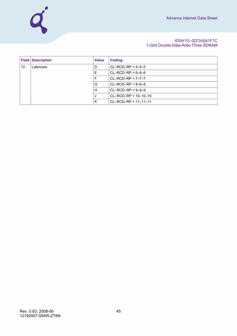
12 Latencies D CL–RCD–RP = 5–5–5E CL–RCD–RP = 6–6–6F CL–RCD–RP = 7–7–7G CL–RCD–RP = 8–8–8H CL–RCD–RP = 9–9–9J CL–RCD–RP = 10–10–10K CL–RCD–RP = 11–11–11
Field Description Value Coding
Rev. 0.63, 2008-06 4512192007-S9AR-ZT6N

IDSH1G–0[2/3/4]A1F1C1-Gbit Double-Data-Rate-Three SDRAM
Advance Internet Data Sheet
List of Illustrations
Figure 1 Ballout for 1Gb ×4 Components (PG-TFBGA-78). . . . . . . . . . . . . . . . . . . . . . . . . . . . . . . . . . . . . . . . . . . . . . . . 6Figure 2 Ballout for 1Gb × 8 Components (PG-TFBGA-78) . . . . . . . . . . . . . . . . . . . . . . . . . . . . . . . . . . . . . . . . . . . . . . . 7Figure 3 Ballout for 1Gb × 16 Components (PG-TFBGA-96) . . . . . . . . . . . . . . . . . . . . . . . . . . . . . . . . . . . . . . . . . . . . . . 8Figure 4 Reference Load for AC Timings and Output Slew Rates . . . . . . . . . . . . . . . . . . . . . . . . . . . . . . . . . . . . . . . . . 26Figure 5 AC Overshoot / Undershoot Definitions for Address and Control Signals . . . . . . . . . . . . . . . . . . . . . . . . . . . . 34Figure 6 AC Overshoot / Undershoot Definitions for Clock, Data, Strobe and Mask Signals . . . . . . . . . . . . . . . . . . . . . 35Figure 7 Package Outlines. Left: PG-TFBGA-78 (x4/x8). Right: PG-TFBGA-96 (x16) . . . . . . . . . . . . . . . . . . . . . . . . . . 43
Rev. 0.63, 2008-06 4612192007-S9AR-ZT6N

IDSH1G–0[2/3/4]A1F1C1-Gbit Double-Data-Rate-Three SDRAM
Advance Internet Data Sheet
List of Tables
Table 1 Ordering Information . . . . . . . . . . . . . . . . . . . . . . . . . . . . . . . . . . . . . . . . . . . . . . . . . . . . . . . . . . . . . . . . . . . . . . 4Table 2 1-Gbit DDR3 SDRAM Addressing . . . . . . . . . . . . . . . . . . . . . . . . . . . . . . . . . . . . . . . . . . . . . . . . . . . . . . . . . . . 5Table 3 Input / Output Signal Functional Description. . . . . . . . . . . . . . . . . . . . . . . . . . . . . . . . . . . . . . . . . . . . . . . . . . . . 9Table 4 Command Truth Table . . . . . . . . . . . . . . . . . . . . . . . . . . . . . . . . . . . . . . . . . . . . . . . . . . . . . . . . . . . . . . . . . . . 11Table 5 Clock Enable (CKE) Truth Table for Synchronous Transitions. . . . . . . . . . . . . . . . . . . . . . . . . . . . . . . . . . . . . 13Table 6 Data Mask (DM) Truth Table . . . . . . . . . . . . . . . . . . . . . . . . . . . . . . . . . . . . . . . . . . . . . . . . . . . . . . . . . . . . . . 14Table 7 MR0 Mode register Definition (BA[2:0]=000B) . . . . . . . . . . . . . . . . . . . . . . . . . . . . . . . . . . . . . . . . . . . . . . . . . 15Table 8 MR1 Mode Register Definition (BA[2:0]=001B) . . . . . . . . . . . . . . . . . . . . . . . . . . . . . . . . . . . . . . . . . . . . . . . . . 17Table 9 MR2 Mode Register Definition (BA[2:0]=010B) . . . . . . . . . . . . . . . . . . . . . . . . . . . . . . . . . . . . . . . . . . . . . . . . . 19Table 10 MR3 Mode Register Definition (BA[2:0]=011B) . . . . . . . . . . . . . . . . . . . . . . . . . . . . . . . . . . . . . . . . . . . . . . . . . 21Table 11 Bit Order during Burst . . . . . . . . . . . . . . . . . . . . . . . . . . . . . . . . . . . . . . . . . . . . . . . . . . . . . . . . . . . . . . . . . . . . 22Table 12 Absolute Maximum Ratings . . . . . . . . . . . . . . . . . . . . . . . . . . . . . . . . . . . . . . . . . . . . . . . . . . . . . . . . . . . . . . . 24Table 13 SDRAM Component Operating Temperature Range . . . . . . . . . . . . . . . . . . . . . . . . . . . . . . . . . . . . . . . . . . . . 25Table 14 DC Operating Conditions . . . . . . . . . . . . . . . . . . . . . . . . . . . . . . . . . . . . . . . . . . . . . . . . . . . . . . . . . . . . . . . . . 25Table 15 Input and Output Leakage Currents . . . . . . . . . . . . . . . . . . . . . . . . . . . . . . . . . . . . . . . . . . . . . . . . . . . . . . . . . 26Table 16 DC and AC Input Levels for Single-Ended Command, Address and Control Signals . . . . . . . . . . . . . . . . . . . 27Table 17 DC and AC Input Levels for Single-Ended DQ and DM Signals. . . . . . . . . . . . . . . . . . . . . . . . . . . . . . . . . . . . 27Table 18 Differential Swing Requirement for Clock (CK - CK) and Strobe (DQS - DQS) . . . . . . . . . . . . . . . . . . . . . . . . 28Table 19 Allowed Time Before Ringback (tDVAC) for CLK - CLK and DQS - DQS . . . . . . . . . . . . . . . . . . . . . . . . . . . . . . 28Table 20 Each Single-Ended Levels for CK, CK, DQS, DQS, DQSL, DQSL, DQSU or DQSU . . . . . . . . . . . . . . . . . . . 29Table 21 Cross Point Voltage for Differential Input Signals (CK, DQS). . . . . . . . . . . . . . . . . . . . . . . . . . . . . . . . . . . . . . 29Table 22 DC and AC Output Levels for Single-Ended Signals . . . . . . . . . . . . . . . . . . . . . . . . . . . . . . . . . . . . . . . . . . . . 30Table 23 AC Output Levels for Differential Signals . . . . . . . . . . . . . . . . . . . . . . . . . . . . . . . . . . . . . . . . . . . . . . . . . . . . . 30Table 24 ODT DC Impedance and Mid-Level Characteristics . . . . . . . . . . . . . . . . . . . . . . . . . . . . . . . . . . . . . . . . . . . . . 31Table 25 ODT DC Impedance after proper IO Calibration and Voltage/Temperature Drift . . . . . . . . . . . . . . . . . . . . . . . 31Table 26 OTD DC Impedance Sensitivity Parameters. . . . . . . . . . . . . . . . . . . . . . . . . . . . . . . . . . . . . . . . . . . . . . . . . . . 32Table 27 Output Slew Rates . . . . . . . . . . . . . . . . . . . . . . . . . . . . . . . . . . . . . . . . . . . . . . . . . . . . . . . . . . . . . . . . . . . . . . 32Table 28 Interface Capacitance Values . . . . . . . . . . . . . . . . . . . . . . . . . . . . . . . . . . . . . . . . . . . . . . . . . . . . . . . . . . . . . . 33Table 29 AC Overshoot / Undershoot Specification for Address and Control Signals. . . . . . . . . . . . . . . . . . . . . . . . . . . 34Table 30 AC Overshoot / Undershoot Specification for Clock, Data, Strobe and Mask Signals . . . . . . . . . . . . . . . . . . . 34Table 31 DDR3-800 Speed Bins and Operating Conditions . . . . . . . . . . . . . . . . . . . . . . . . . . . . . . . . . . . . . . . . . . . . . . 37Table 32 DDR3-1066 Speed Bins and Operating Conditions . . . . . . . . . . . . . . . . . . . . . . . . . . . . . . . . . . . . . . . . . . . . . 38Table 33 DDR3-1333 Speed Bins and Operating Conditions . . . . . . . . . . . . . . . . . . . . . . . . . . . . . . . . . . . . . . . . . . . . . 39Table 34 DDR3-1600 Speed Bins and Operating Conditions . . . . . . . . . . . . . . . . . . . . . . . . . . . . . . . . . . . . . . . . . . . . . 40Table 35 DDR3-DLL_off Speed Bins and Operating Conditions . . . . . . . . . . . . . . . . . . . . . . . . . . . . . . . . . . . . . . . . . . . 42Table 36 Example for Nomenclature Fields. . . . . . . . . . . . . . . . . . . . . . . . . . . . . . . . . . . . . . . . . . . . . . . . . . . . . . . . . . . 44Table 37 DDR3 SDRAM Nomenclature. . . . . . . . . . . . . . . . . . . . . . . . . . . . . . . . . . . . . . . . . . . . . . . . . . . . . . . . . . . . . . 44
Rev. 0.63, 2008-06 4712192007-S9AR-ZT6N

IDSH1G–0[2/3/4]A1F1C1-Gbit Double-Data-Rate-Three SDRAM
Advance Internet Data Sheet
Contents
1 Overview . . . . . . . . . . . . . . . . . . . . . . . . . . . . . . . . . . . . . . . . . . . . . . . . . . . . . . . . . . . . . . . . . . . . . . . . . . . . . . . . . 31.1 Features . . . . . . . . . . . . . . . . . . . . . . . . . . . . . . . . . . . . . . . . . . . . . . . . . . . . . . . . . . . . . . . . . . . . . . . . . . . . . . . . . . 31.2 Product List. . . . . . . . . . . . . . . . . . . . . . . . . . . . . . . . . . . . . . . . . . . . . . . . . . . . . . . . . . . . . . . . . . . . . . . . . . . . . . . . 41.3 DDR3 SDRAM Addressing. . . . . . . . . . . . . . . . . . . . . . . . . . . . . . . . . . . . . . . . . . . . . . . . . . . . . . . . . . . . . . . . . . . . 51.4 Package Ballout . . . . . . . . . . . . . . . . . . . . . . . . . . . . . . . . . . . . . . . . . . . . . . . . . . . . . . . . . . . . . . . . . . . . . . . . . . . . 61.5 Input / Output Signal Functional Description . . . . . . . . . . . . . . . . . . . . . . . . . . . . . . . . . . . . . . . . . . . . . . . . . . . . . . 9
2 Functional Description. . . . . . . . . . . . . . . . . . . . . . . . . . . . . . . . . . . . . . . . . . . . . . . . . . . . . . . . . . . . . . . . . . . . . 112.1 Truth Tables . . . . . . . . . . . . . . . . . . . . . . . . . . . . . . . . . . . . . . . . . . . . . . . . . . . . . . . . . . . . . . . . . . . . . . . . . . . . . . 112.2 Mode Register 0 (MR0). . . . . . . . . . . . . . . . . . . . . . . . . . . . . . . . . . . . . . . . . . . . . . . . . . . . . . . . . . . . . . . . . . . . 152.3 Mode Register 1 (MR1). . . . . . . . . . . . . . . . . . . . . . . . . . . . . . . . . . . . . . . . . . . . . . . . . . . . . . . . . . . . . . . . . . . . 172.4 Mode Register 2 (MR2). . . . . . . . . . . . . . . . . . . . . . . . . . . . . . . . . . . . . . . . . . . . . . . . . . . . . . . . . . . . . . . . . . . . 192.5 Mode Register 3 (MR3). . . . . . . . . . . . . . . . . . . . . . . . . . . . . . . . . . . . . . . . . . . . . . . . . . . . . . . . . . . . . . . . . . . . 212.6 Read / Write Operations and Access Modes . . . . . . . . . . . . . . . . . . . . . . . . . . . . . . . . . . . . . . . . . . . . . . . . . . . . . 222.6.1 Burst Order . . . . . . . . . . . . . . . . . . . . . . . . . . . . . . . . . . . . . . . . . . . . . . . . . . . . . . . . . . . . . . . . . . . . . . . . . . . 22
3 Operating Conditions and Interface Specification . . . . . . . . . . . . . . . . . . . . . . . . . . . . . . . . . . . . . . . . . . . . . . 243.1 Absolute Maximum Ratings . . . . . . . . . . . . . . . . . . . . . . . . . . . . . . . . . . . . . . . . . . . . . . . . . . . . . . . . . . . . . . . . . . 243.2 Operating Conditions . . . . . . . . . . . . . . . . . . . . . . . . . . . . . . . . . . . . . . . . . . . . . . . . . . . . . . . . . . . . . . . . . . . . . . . 253.3 Interface Test Conditions . . . . . . . . . . . . . . . . . . . . . . . . . . . . . . . . . . . . . . . . . . . . . . . . . . . . . . . . . . . . . . . . . . . . 263.4 Voltage Levels . . . . . . . . . . . . . . . . . . . . . . . . . . . . . . . . . . . . . . . . . . . . . . . . . . . . . . . . . . . . . . . . . . . . . . . . . . . . 273.4.1 DC and AC Logic Input Levels . . . . . . . . . . . . . . . . . . . . . . . . . . . . . . . . . . . . . . . . . . . . . . . . . . . . . . . . . . . . . . 273.4.2 DC and AC Output Measurements Levels . . . . . . . . . . . . . . . . . . . . . . . . . . . . . . . . . . . . . . . . . . . . . . . . . . . . . 303.5 ODT DC Impedance and Mid-Level Characteristics . . . . . . . . . . . . . . . . . . . . . . . . . . . . . . . . . . . . . . . . . . . . . . 313.6 ODT DC Impedance Sensitivity on Temperature and Voltage Drifts . . . . . . . . . . . . . . . . . . . . . . . . . . . . . . . . . 313.7 Output Slew Rate Definition and Requirements . . . . . . . . . . . . . . . . . . . . . . . . . . . . . . . . . . . . . . . . . . . . . . . . . . . 323.7.1 Output Slew Rates . . . . . . . . . . . . . . . . . . . . . . . . . . . . . . . . . . . . . . . . . . . . . . . . . . . . . . . . . . . . . . . . . . . . . . . 323.8 Interface Capacitance. . . . . . . . . . . . . . . . . . . . . . . . . . . . . . . . . . . . . . . . . . . . . . . . . . . . . . . . . . . . . . . . . . . . . . . 333.9 Overshoot and Undershoot Specification . . . . . . . . . . . . . . . . . . . . . . . . . . . . . . . . . . . . . . . . . . . . . . . . . . . . . . . . 34
4 Speed Bins and Timing Parameters . . . . . . . . . . . . . . . . . . . . . . . . . . . . . . . . . . . . . . . . . . . . . . . . . . . . . . . . . . 364.1 Speed Bins . . . . . . . . . . . . . . . . . . . . . . . . . . . . . . . . . . . . . . . . . . . . . . . . . . . . . . . . . . . . . . . . . . . . . . . . . . . . . . . 36
5 Package Outline . . . . . . . . . . . . . . . . . . . . . . . . . . . . . . . . . . . . . . . . . . . . . . . . . . . . . . . . . . . . . . . . . . . . . . . . . . 43
6 Product Type Nomenclature . . . . . . . . . . . . . . . . . . . . . . . . . . . . . . . . . . . . . . . . . . . . . . . . . . . . . . . . . . . . . . . . 44
Rev. 0.63, 2008-06 4812192007-S9AR-ZT6N

Advance Internet Data Sheet
Edition 2008-06Published by Qimonda AGGustav-Heinemann-Ring 212D-81739 München, Germany© Qimonda AG 2008.All Rights Reserved.
Legal DisclaimerTHE INFORMATION GIVEN IN THIS INTERNET DATA SHEET SHALL IN NO EVENT BE REGARDED AS A GUARANTEE OF CONDITIONS OR CHARACTERISTICS. WITH RESPECT TO ANY EXAMPLES OR HINTS GIVEN HEREIN, ANY TYPICAL VALUES STATED HEREIN AND/OR ANY INFORMATION REGARDING THE APPLICATION OF THE DEVICE, QIMONDA HEREBY DISCLAIMS ANY AND ALL WARRANTIES AND LIABILITIES OF ANY KIND, INCLUDING WITHOUT LIMITATION WARRANTIES OF NON-INFRINGEMENT OF INTELLECTUAL PROPERTY RIGHTS OF ANY THIRD PARTY.
InformationFor further information on technology, delivery terms and conditions and prices please contact your nearest Qimonda Office.
WarningsDue to technical requirements components may contain dangerous substances. For information on the types in question please contact your nearest Qimonda Office.Qimonda Components may only be used in life-support devices or systems with the express written approval of Qimonda, if a failure of such components can reasonably be expected to cause the failure of that life-support device or system, or to affect the safety or effectiveness of that device or system. Life support devices or systems are intended to be implanted in the human body, or to support and/or maintain and sustain and/or protect human life. If they fail, it is reasonable to assume that the health of the user or other persons may be endangered.
www.qimonda.com
![4Gb D-die DDR3 SDRAM- 5 - K4B4G0846D datasheet DDR3 SDRAM Rev. 1.23 K4B4G0446D 1. Ordering Information [ Table 1 ] Samsung 4Gb DDR3 D-die ordering information table NOTE: 1. Speed](https://static.fdocuments.net/doc/165x107/5e73e86eb6f1e10b075d492a/4gb-d-die-ddr3-sdram-5-k4b4g0846d-datasheet-ddr3-sdram-rev-123-k4b4g0446d.jpg)


![2Gb C-die DDR3 SDRAM Industrial€¦ · datasheet DDR3 SDRAM Rev. 1.0 K4B2G1646C Industrial 1. Ordering Information [ Table 1 ] Samsung 2Gb DDR3 C-die ordering information table NOTE:](https://static.fdocuments.net/doc/165x107/5ecc8b7cc35ff9103a633f0f/2gb-c-die-ddr3-sdram-datasheet-ddr3-sdram-rev-10-k4b2g1646c-industrial-1-ordering.jpg)


![2Gb C-die DDR3 SDRAM Only x16 - BDTIC · DDR3 SDRAM Addressing ... [ Table 1 ] Samsung 2Gb DDR3 C-die ordering information table. NOTE: 1. Speed bin is in order of CL-tRCD-tRP. 2.](https://static.fdocuments.net/doc/165x107/5ad5dbf67f8b9a5c638d9a9d/2gb-c-die-ddr3-sdram-only-x16-sdram-addressing-table-1-samsung-2gb-ddr3.jpg)


![4Gb E-die DDR3 SDRAM - samsung.com · - 5 - K4B4G0846E datasheet DDR3 SDRAM Rev. 1.2 K4B4G0446E 1. Ordering Information [ Table 1 ] Samsung 4Gb DDR3 E-die ordering information table](https://static.fdocuments.net/doc/165x107/5dd0e76fd6be591ccb634357/4gb-e-die-ddr3-sdram-5-k4b4g0846e-datasheet-ddr3-sdram-rev-12-k4b4g0446e.jpg)