
ICE1PCS01 - 300 W / 500 W CCM-PFC Demonstration Board · ICE1PCS01 - 300 W / 500 W CCM-PFC...
25
Application Note, V1.0, June 2003 Power Management & Supply Never stop thinking. ICE1PCS01 - 300 W / 500 W CCM-PFC Demonstration Board AN-EVAL-ICE1PCS01-1 Author: Bernd Ilchmann, Finepower GmbH Wolfgang Frank, Infineon http://www.infineon.com/pfc
Transcript of ICE1PCS01 - 300 W / 500 W CCM-PFC Demonstration Board · ICE1PCS01 - 300 W / 500 W CCM-PFC...

Appl icat ion Note, V1.0, June 2003
Power Management & Supply
N e v e r s t o p t h i n k i n g .
ICE1PCS01 -
300 W / 500 W CCM-PFC Demonstrat ion BoardAN-EVAL-ICE1PCS01-1
Author: Bernd Ilchmann, Finepower GmbH Wolfgang Frank, Infineon
http://www.infineon.com/pfc

Edition 2003-06
Published by Infineon Technologies AG,St.-Martin-Strasse 53,81669 München, Germany
© Infineon Technologies AG 2002.All Rights Reserved.
Attention please!
The information herein is given to describe certain components and shall not be considered as warranted characteristics.Terms of delivery and rights to technical change reserved.We hereby disclaim any and all warranties, including but not limited to warranties of non-infringement, regarding circuits, descriptions and charts stated herein.Infineon Technologies is an approved CECC manufacturer.
Information
For further information on technology, delivery terms and conditions and prices please contact your nearest Infineon Technologies Office in Germany or our Infineon Technologies Representatives worldwide.
Warnings
Due to technical requirements components may contain dangerous substances. For information on the types in question please contact your nearest Infineon Technologies Office.Infineon Technologies Components may only be used in life-support devices or systems with the express written approval of Infineon Technologies, if a failure of such components can reasonably be expected to cause the failure of that life-support device or system, or to affect the safety or effectiveness of that device or system. Life-support devices or systems are intended to be implanted in the human body, or to support and/or maintain and sustain and/or protect human life. If they fail, it is reasonable to assume that the health of the user or other persons may be endangered.
For questions on technology, delivery and prices please contact the InfineonTechnologies Offices in Germany or the Infineon Technologies Companies andRepresentatives worldwide: see our webpage at http://www.infineon.com.
CoolMOSTM, CoolSETTM are a trademarks of Infineon Technologies AG.
ICE1PCS01 - 300 W / 500 W CCM-PFC Demonstration Board Revision History: 2003-06 V1.0
Previous Version:
Page Subjects (major changes since last revision)
10 equation 3
11 equation 5

ICE1PCS01 - 300 W / 500 W CCM-PFC DemonstrationBoard
Application Note 1 V1.0, 2003-06
1 Short Description . . . . . . . . . . . . . . . . . . . . . . . . . . . . . . . . . . . . . . . . . . . . 6
2 Features . . . . . . . . . . . . . . . . . . . . . . . . . . . . . . . . . . . . . . . . . . . . . . . . . . . 7
3 Functional Description . . . . . . . . . . . . . . . . . . . . . . . . . . . . . . . . . . . . . . . 8
4 Description of Functional Blocks . . . . . . . . . . . . . . . . . . . . . . . . . . . . . . . 94.1 AC-input filter / EMI-Filter . . . . . . . . . . . . . . . . . . . . . . . . . . . . . . . . . . . . . 104.2 PFC Power Stage . . . . . . . . . . . . . . . . . . . . . . . . . . . . . . . . . . . . . . . . . . . 104.3 PFC-Controller . . . . . . . . . . . . . . . . . . . . . . . . . . . . . . . . . . . . . . . . . . . . . . 114.3.1 Calculation of Shunt Resistor . . . . . . . . . . . . . . . . . . . . . . . . . . . . . . . . 124.3.2 Ouput Voltage setting . . . . . . . . . . . . . . . . . . . . . . . . . . . . . . . . . . . . . . 134.3.3 Current Control loop compensation . . . . . . . . . . . . . . . . . . . . . . . . . . . . 134.3.4 Setting of the voltage loop compensation . . . . . . . . . . . . . . . . . . . . . . . 144.3.5 Setting of the switching frequency . . . . . . . . . . . . . . . . . . . . . . . . . . . . . 144.3.6 Device turn-off . . . . . . . . . . . . . . . . . . . . . . . . . . . . . . . . . . . . . . . . . . . . 14
5 Construction . . . . . . . . . . . . . . . . . . . . . . . . . . . . . . . . . . . . . . . . . . . . . . 15
6 Test results and EMI-behaviour . . . . . . . . . . . . . . . . . . . . . . . . . . . . . . . 176.1 Test Setup . . . . . . . . . . . . . . . . . . . . . . . . . . . . . . . . . . . . . . . . . . . . . . . . . 176.2 Efficiency and Power losses . . . . . . . . . . . . . . . . . . . . . . . . . . . . . . . . . . . 176.3 EMI and Power Factor . . . . . . . . . . . . . . . . . . . . . . . . . . . . . . . . . . . . . . . . 186.3.1 EMI . . . . . . . . . . . . . . . . . . . . . . . . . . . . . . . . . . . . . . . . . . . . . . . . . . . . 186.3.2 Power factor . . . . . . . . . . . . . . . . . . . . . . . . . . . . . . . . . . . . . . . . . . . . . . 19
7 PCB . . . . . . . . . . . . . . . . . . . . . . . . . . . . . . . . . . . . . . . . . . . . . . . . . . . . . . 21
8 Bill of Material . . . . . . . . . . . . . . . . . . . . . . . . . . . . . . . . . . . . . . . . . . . . . 23
9 Summary of Used Nomenclature . . . . . . . . . . . . . . . . . . . . . . . . . . . . . . 25
10 References . . . . . . . . . . . . . . . . . . . . . . . . . . . . . . . . . . . . . . . . . . . . . . . . 26

AN-EVAL-ICE1PCS01-1ICE1PCS01 - 300 W / 500 W CCM-PFC Demonstration Board
1 Short Description
Figure 1 Photo of Demoboard
This Application note describes a 300 W / 500 W Power Factor Correction (PFC)Demonstration Board working in continuous (inductor-) current mode (CCM). Based onthe Infineon’s device ICE1PCS01 a universal PFC stage with wide input voltage range(90 VAC to 265 VAC) and 400 VDC output is realised on a small PCB. Due to its limitedheatsink capability the high output power of 500 W is only available in the upper inputvoltage range (190 VAC to 265 VAC). If the user likes to use this board in a wide inputrange application a derating of the maximum output power to 300 W is necessary.Figure 1 shows a photo of the demoboard.
Application Note 6 V1.0, 2003-06

ICE1PCS01 - 300 W / 500 W CCM-PFC DemonstrationBoard
2 FeaturesThe CCM-PFC Demonstration Board consists on a small PCB for testing and evaluatingthe performance of the integrated PFC-controller ICE1PCS01 as well as the advancedpower elements (CoolMOS and SiC diode) from Infineon. Due to the chosen powerswitch (SPP21N50C3) and the "lossless" recovering booster diode (SDT04S60) a veryhigh efficiency has been achieved. So the required heatsink keeps small for the givenpower level. Furthermore this board demonstrates a variety of different protectionfeatures and the benefit of a low number of IC related component's for programming theconverter.
.
Technical specification:
Input Voltage Range 90 VAC ... 265 VAC
Output Power 300 W (90 VAC ... 265 VAC)500 W (190 VAC ... 265 VAC)
Output Voltage 400 V 5%
Efficiency (@ POUTNOM) ~ 92% to 97% (see diagram)
Switching Frequency 130 kHz
Power Factor IEC1000-3-2
Conducted Emission EN55011-B
Switching Transistor SPP21N50C3 (CoolMOS )
Boost Diode SDT04S60 (SiC diode)
Application Note 7 V1.0, 2003-06
ICE1PCS01 - 300 W / 500 W CCM-PFC DemonstrationBoard
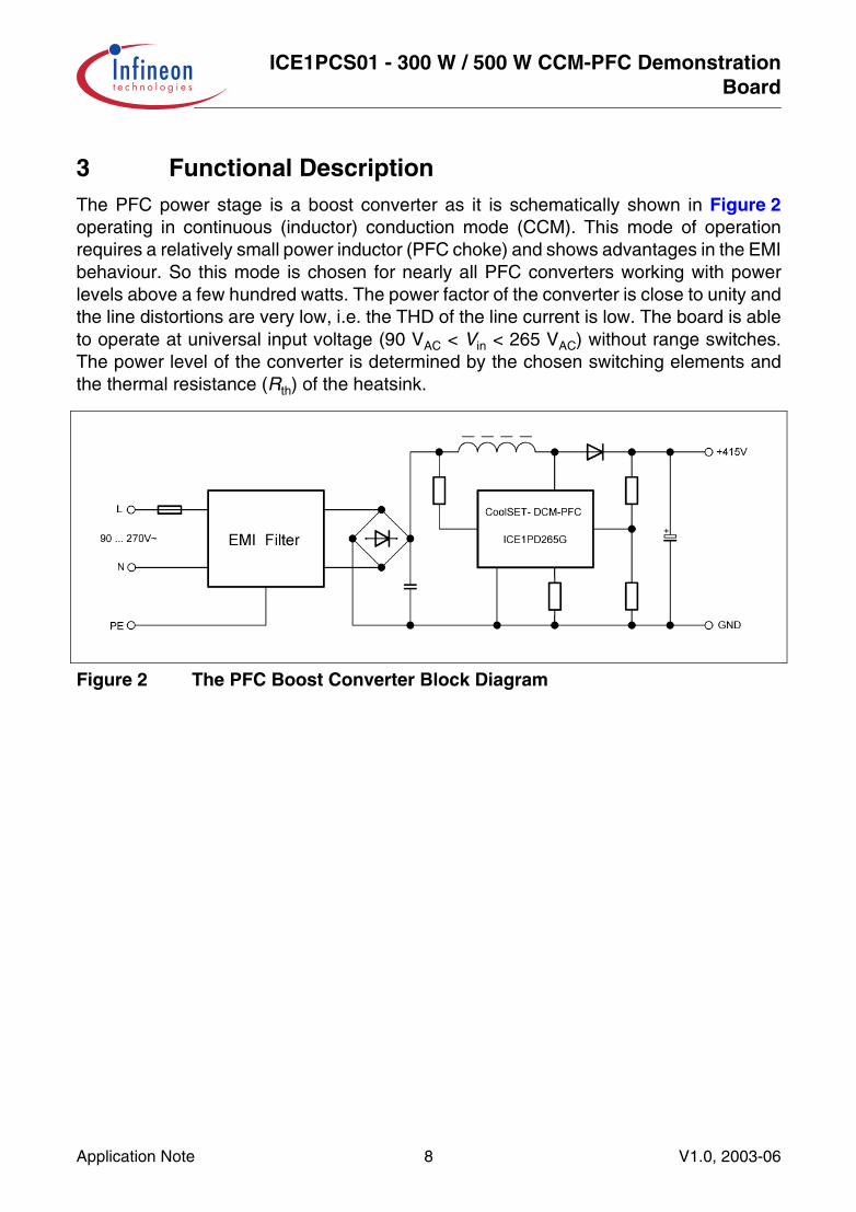
3 Functional DescriptionThe PFC power stage is a boost converter as it is schematically shown in Figure 2operating in continuous (inductor) conduction mode (CCM). This mode of operationrequires a relatively small power inductor (PFC choke) and shows advantages in the EMIbehaviour. So this mode is chosen for nearly all PFC converters working with powerlevels above a few hundred watts. The power factor of the converter is close to unity andthe line distortions are very low, i.e. the THD of the line current is low. The board is ableto operate at universal input voltage (90 VAC < Vin < 265 VAC) without range switches.The power level of the converter is determined by the chosen switching elements andthe thermal resistance (Rth) of the heatsink.
Figure 2 The PFC Boost Converter Block Diagram
Application Note 8 V1.0, 2003-06

ICE1PCS01 - 300 W / 500 W CCM-PFC DemonstrationBoard
4 Description of Functional Blocks
Figure 3 Schematic of the PFC demonstration board
Application Note 9 V1.0, 2003-06

ICE1PCS01 - 300 W / 500 W CCM-PFC DemonstrationBoard
4.1 AC-input filter / EMI-Filter
The input voltage for the PFC board is 90 VAC to 265 VAC (50 / 60 Hz). A fuse preventsthe board from burning in case of catastrophic failure. The line EMI Filter (C1, C6, C7,C8, L2) suppresses the high frequency noise caused by the switching elements. The linerectifier as well as the EMI common mode choke are designed to handle the maximuminput line current at rated load without saturation or excessive power losses.
4.2 PFC Power Stage
The main elements of the boost type PFC-converter are L1, T1, D1 and C2 according toFigure 3.
D2 bypasses the inrush current to the bulk. So it prevents especially the PFC diode fromexcessive surge current.
For the boost inductor L1 a MPP toroide core from Magnetics is used. The winding ismade in a single layer of tree copper wires in parallel which reduces the parasitic windingcapacitance as well as the magnetic leakage inductance.
The calculation flow for the boost inductance is described below. The maximum rmsinput current at which the full output power including a overload of 5% (i.e. 15 W) has tobe provided is
(1)
In this point of operation the voltage across the boost inductor during turn-on is:
(2)
The related duty cycle for the given output voltage is calculated below:
(3)
The peak to peak current ripple (switching frequency) in the inductor is between 20% and30% of the maximum peak line current. Expecting a value of 30% the ripple current is
IL1 PK( )2 Poutmax POL+( )⋅
η Vinmin⋅-------------------------------------------------------- 2 300W 15W+( )⋅
0 92, 90⋅ V---------------------------------------------------- 5 38A,= = =
VINminPK 2 90V⋅ 127V= =
dVout VINminPK–
VOUT------------------------------------------ 400V 127V–
400V---------------------------------- 0 68,= = =
Application Note 10 V1.0, 2003-06

ICE1PCS01 - 300 W / 500 W CCM-PFC DemonstrationBoard
around 1,61A. The time when the input current charges L1 is the switching time tON ofthe MOSFET:
(4)
Now the inductor value can be estimated:
(5)
The toroide core 55083 from Magnetics is a MPP material which shows low AC fluxlosses and is able to handle the chosen switching frequency at the rated current. TheAL- value of this core is 81nH, so that 71 turns are necessary to give the requiredinductance IL1(PK). The full load inductance is a little bit less due to AL derating by fluxdensity but, in practice, this part works very well in the given application. Thetemperature rising under full load condition is less than 50 degrees. An other approachwould lead to a bigger core which would be oversized in terms of losses and cost.
The switching transistor T1 is a 21A / 190 mΩ CoolMOS transistor (SPP21N50C3) fromInfineon which is able to handle the maximum input current without excessive losses. Itis driven directly from the gate drive output of the PFC controller. The TO-220 packageas well as the other power elements (Br1 and D1) are thermally connected to a commonheatsink using thermal pads with a low thermal resistance (Transtherm ) .
The boost diode D1 is a SDP04S60 silicon carbide diode (thinQ! ) from Infineon. In termsof recovery behaviour this diode is very close to an ideal diode. Due to its negligiblerecovery time and reverse current the switching transistor profits a big benefit. Theincreased efficiency of the PFC stage compared with other traditional designs is mainlycaused by the SiC diode.
The output bulk capacitor is a 450 V device. For general purpose its typical size shouldbe chosen by approximately 0.25 to 1 µF/Watt. However, there could be applicationdependent variations. Especially the hold up time in combination with the second stageconverter's input range can require other values. The limitation in size is the capability tohandle the maximum ripple current at switching frequency.
4.3 PFC-Controller
The new CCM-PFC controller ICE1PCS01 combines an enhanced functionality with alow number of pins and IC related external components. Furthermore, the programmingof the function as well as the compensation of the internal error amplifiers is very easy.A lot of intelligent protection features help to save the power elements from damage.
tOND
fSW--------- 0 68,
130kHz--------------------- 5 23µs,= = =
L1VINminPK tON⋅
∆I-------------------------------------- 127V 5 23µs,⋅
1 61A,--------------------------------------- 412µH= = =
Application Note 11 V1.0, 2003-06

ICE1PCS01 - 300 W / 500 W CCM-PFC DemonstrationBoard
The controller includes all function blocks for controlling a sinusoidal input currentmeeting the IEC1000-3-2 standard. Exceeding the primary function in controlling thepower factor some special features for safe operation are integrated:
• UVLO with internally pull down during off state• Frequency setting by a simple resistor to ground• Leading edge modulation for reducing the bulk ripple current when synchronized• Adaptive, automatic soft start to protect the booster diode from excessive dissipation• Brownout protection (BOP) by reducing the bus voltage• Soft over current control (SOC)• Peak current limitation (PCL)• Open loop protection (OLP) / input under voltage detect / remote off function• Output under voltage detection (OUV)• Over Voltage Protection (OVP)• No input voltage waveform sensing necessary
The IC block diagram, its electrical parameters and the exact description is given by thedatasheet [1]. A further Application Note "ICE1PCS01 - Getting Started" [2] is availablewhich gives a lot of relations for setting the elements and the IC function.
4.3.1 Calculation of Shunt Resistor
The only one element to limit the maximum input power is the current sense resistor(R1). Its voltage drop related with the input current is compared by two thresholds withinthe IC. The first threshold (700mV) limits the maximum input current signal used forregulation. The second threshold (set by 1V) gives an independent level for peak currentlimitation. The current sense resistor is set by the following relations:
• Minimum input voltage: VIN(MIN) = 90VAC• Estimated efficiency @ VIN(MIN): = 92%• Rated output power @ low line: POUT(MAX) = 300W • Factor of overload headroom: kOL = 1,05• Factor of inductor ripple current: kIRP = 1,15
The maximum input current including the inductor ripple and 5% overload is
(6)
This value has to correspond with the maximum current sense level for regulation (0,7V).So RCS can calculated:
(7)
IINmax
PINmin 2⋅η VINmin⋅
----------------------------- kOL kIRP⋅ ⋅ 300W 2⋅0 92 90V⋅,---------------------------- 1 15, 1 05,⋅ ⋅ 6 19A,= = =
RCS0 7V,IINmax---------------- 0 7V,
6 19A,----------------- 113mΩ= = =
Application Note 12 V1.0, 2003-06

ICE1PCS01 - 300 W / 500 W CCM-PFC DemonstrationBoard
A low-inductance current sense resistor of 100mΩ was chosen. The max. dissipationpower is less than 2 W.
4.3.2 Ouput Voltage setting
The output voltage is set by the voltage divider R3A, R3B and R4. Due to the high outputvoltage (400 V) a splitting of the upper resistor is recommended to limit the voltagestress. The value of R4 is chosen with 5.6 kΩ. The high side resistor can calculate now:
(8)
Splitting this value in 2 equal parts leads to 221kΩ for each. When the next value of theE12-series is chosen (220 kΩ) the error is around 0.5%. This leads to a resulting outputvoltage and overvoltage level of
(9)
(10)
The output voltage is close enough to the rated value of 400 V. The value around 420 Vfor the overvoltage protection is properly to protect the output electrolytic capacitor aswell as the switching components.
4.3.3 Current Control loop compensation
The inner current control loop of the PFC stage is managed by OTA2 according to theIC block diagram in the datasheet [1]. The compensation is quite easy because the onlyone variable element is the switching frequency of the converter. The value of thecompensation capacitor C3 has a direct influence to the total harmonic distorsion (THD)of the input current waveform.
(11)
In this application C3 is chosen with 2,2 nF. The added capacitor value (0,5 ... 1 nF) iscaused by the non-linear gain behaviour of the current function block.
R3Vout VREF–
VREF------------------------------- R4⋅ 400V 5V–
5V---------------------------- 5 6kΩ,⋅ 422kΩ= = =
VOUTnomR3 R4+
R4----------------------- VREF⋅ 5 6kΩ 440kΩ+,
5 6kΩ,------------------------------------------- 5V⋅ 397 8V,= = =
VOUTOVPR3 R4+
R4----------------------- VOVP⋅ 5 6kΩ 440kΩ+,
5 6kΩ,------------------------------------------- 5 25V,⋅ 417 75V,= = =
C3gOTA2
2π fSW⋅--------------------- 0 5…1nF,( )+ 1 1mS,
2π 130kHz⋅-------------------------------- 0 5…1nF,( )+ 1 8…2 3nF,,= = =
Application Note 13 V1.0, 2003-06

ICE1PCS01 - 300 W / 500 W CCM-PFC DemonstrationBoard
4.3.4 Setting of the voltage loop compensation
More exactly the relations for compensating the voltage loop are given in [2]. By physicsof active power factor correction there is a voltage ripple on the output capacitor (C2)having twice the line frequency. By definition, the voltage error amplifier may not acceptthis ripple as an error signal. Therefore, the only one related signal of the voltage erroramplifier is the average DC bus voltage. So a compensation network on the OTA outputis necessary to separate the error signal from the twice of the line frequency.
With the compensation network of C4 = 1 µF, C5 = 100 nF and R6 = 10 k in combinationwith the OTA's gain of 40 mS the bandwidth is limited to 6,2 Hz which is a goodcompromise between line current distortion and dynamic of the voltage regulation loop.
4.3.5 Setting of the switching frequency
The internal oscillator is programmed by an external resistor R5 to ground. Given by thedatasheet a resistor value of 33 kΩ leads to a switching frequency of approximately125kHz. This switching frequency is chosen by EMI reasons as well as by boost inductorsize and dissipation considerations.
A switching frequency around 130 kHz is out of the range for line conducted emissiongiven by the EN55011 standard. Furthermore this switching frequency gives a highefficiency due to limitation of switching losses in the power switch and, last but not leastthe inductor size and cost benefits.
4.3.6 Device turn-off
The device can be turned off by applying a voltage in the range of 5 V - 15 V the top pinof the middle connector X2 according Figure 12. The signal triggers a transistor whichwill pull down pin 5 (VSENSE) below a level of 0,8 V. This forces the IC into open loopprotection and the IC will stop operation immediately.
Application Note 14 V1.0, 2003-06

ICE1PCS01 - 300 W / 500 W CCM-PFC DemonstrationBoard
5 ConstructionThe 300 W / 500 W CCM-PFC demonstration board is designed on a PBC using throughhole elements only. Approximately 40% of the board space is used for the input line filterwhich suppresses the conducted EMI close to the EN55011 class B level. Due to thechosen EMI concept of this board the heatsink is connected to power ground of the PFCstage and is line connected therefore.
A standard heatsink is used for thermal management of the dissipating semiconductors.Its board mounting is made via distance elements to avoid short between the heatsinkand solder pads. For improved thermal transfer the power semiconductors are isolatedby thermal conductive foils which provide a low thermal resistance Rth.
The three screwless connectors are for input voltage, bias voltage and output voltage aswell for a (logic high) remote-off signal. An external bias supply is necessary to supplythe PFC controller including its driver stage with power. Its value reaches from 12 VDC to14 VDC. Each lab power supply with a stabilized voltage in this range will be fit forevaluation with this board.
A special solution for supplying a professional system with (bias) power is to use theInfineon's CoolBIAS module.
Figure 4 Block diagram of a 2 stage power supply using the CoolBIAS module
Figure 4 shows, that often an independent auxiliary bias supply is helpful to supplyPWM's, external MOSFET drivers, supervisory circuits and more on the primary (lineconnected) side as well as elements on the (line isolated) secondary side. In this casethere is a cost effective solution with Infineon's CoolBIAS demonstration board according
Application Note 15 V1.0, 2003-06

ICE1PCS01 - 300 W / 500 W CCM-PFC DemonstrationBoard
to Figure 5, which can ordered separately. This small board consists on a flyback circuitproviding two 12V outputs (primary and secondary) with a maximum output power of 6watts. Its input voltage is 100 VDC to 400 VDC.
Figure 5 CoolBIAS demonstration board
The complete description of this board can be found in [3]. For special interests inmodification ask Finepower GmbH to find on: http://www.finepower.com
Application Note 16 V1.0, 2003-06

ICE1PCS01 - 300 W / 500 W CCM-PFC DemonstrationBoard
6 Test results and EMI-behaviour
6.1 Test Setup
Usually, there is no application for any PFC stage without electronic load. Typically oneor more DC/DC converter(s), lamp ballast or frequency inverter are connected to thePFC DC output bus. However, for documentation and to avoid any interaction betweenthe PFC stage and the following electronic system a resistive load has been usedaccording to Figure 6.
Figure 6 Test setup for basic electrical parameters
6.2 Efficiency and Power losses
The efficiency is dependent on a lot of different influences. There are voltage dropsacross the input line filter, rectifier, shunt and the copper winding of the choke as well asswitching and conduction losses in power semiconductors. Therefore, in a wide inputrange PFC there is a natural derating of maximum output power for a given design.Usually, any PFC stage can transfer nearly the twice power in the upper input voltagerange than in the wide range.
In this demonstration board the output power is limited by chosen MOSFET, PFC diodeand thermal management. To keep the board and the heatsink small a maximum outputpower of 300 W for the wide range (90 VAC to 265 VAC) and 500 W for the upper inputrange (190 VAC to 265 VAC) was tested.
Application Note 17 V1.0, 2003-06

ICE1PCS01 - 300 W / 500 W CCM-PFC DemonstrationBoard
Figure 7 Efficiency of the 300W / 500W CCM-PFC demonstration board
As discussed the PFC diode has a significant influence on the total performance of thePFC stage. To show this, the 4 A SiC diode from Infineon was replaced by the wellknown 8 A tandem PFC diode STTH806TTI. The reduction in efficiency is more than 1%at low line (90 VAC) according to Figure 7. The additional losses (>3 W) are concentratedin the switching transistor. With the given thermal management (free air) it is impossibleto handle the full output power (300 W) at 90 VAC with this diode. A bigger heatsink orforced cooling would be necessary.
6.3 EMI and Power Factor
6.3.1 EMI
A resistive load at the output - connected with a cable of 1m length - can cause reflectionof noise to the board detecting by the receiver for conducted emission. Nevertheless, thereceiver gives a generally tendency for the noise spectrum caused by the PFC converter.In a real application (PFC output followed by any other switch mode power stage) theinput filter as well as the system noise suppression should be evaluated and modifiedcase by case.
The conducted emission under full load operation measured at 115 VAC with a load of300 W and at 230 VAC with 500 W load is shown in Figure 8 and Figure 9.
y
90,0%
91,0%
92,0%
93,0%
94,0%
95,0%
96,0%
97,0%
98,0%
99,0%
100,0%
90 120 150 180 210 240 270
Input Voltage / Vac
Effc
y. /
%
SiC @ 315WSiC @ 510WSTTH @ 315W
Thermal Runawaydue to high dissipation in the MOSFET
Application Note 18 V1.0, 2003-06

ICE1PCS01 - 300 W / 500 W CCM-PFC DemonstrationBoard
Figure 8 EMI @Vin = 115VAC and Pout = 300 W load
Figure 9 EMI @Vin = 230 VAC and Pout = 500 W load
6.3.2 Power factor
The Power Factor typically depends on the input current, the load and the input voltage.The input filter has therefore an essential influence on the power factor due to its phaseshifting between voltage and current. To meet the EMI standard IEC1000-3-2 the input
Application Note 19 V1.0, 2003-06

ICE1PCS01 - 300 W / 500 W CCM-PFC DemonstrationBoard
current harmonics are the only one criterion. The following plots show the input voltage,current and its spectrum for the rated input voltages.
Figure 10 and Figure 11 show the input voltage, the input current and its harmonics ina linear scale.
Figure 10 VIN, IIN & FFT(IIN) @ VIN = 115 VAC; POUT = 300 W
Figure 11 VIN, IIN & FFT(IIN) @ VIN = 230 VAC; POUT = 500 W
Application Note 20 V1.0, 2003-06

ICE1PCS01 - 300 W / 500 W CCM-PFC DemonstrationBoard
7 PCB
Figure 12 Component placement on the PFC demonstration board
Figure 13 PCB layout (component side)
Application Note 21 V1.0, 2003-06

ICE1PCS01 - 300 W / 500 W CCM-PFC DemonstrationBoard
Figure 14 PCB layout (soldering side - view from component side)
Application Note 22 V1.0, 2003-06
ICE1PCS01 - 300 W / 500 W CCM-PFC DemonstrationBoard
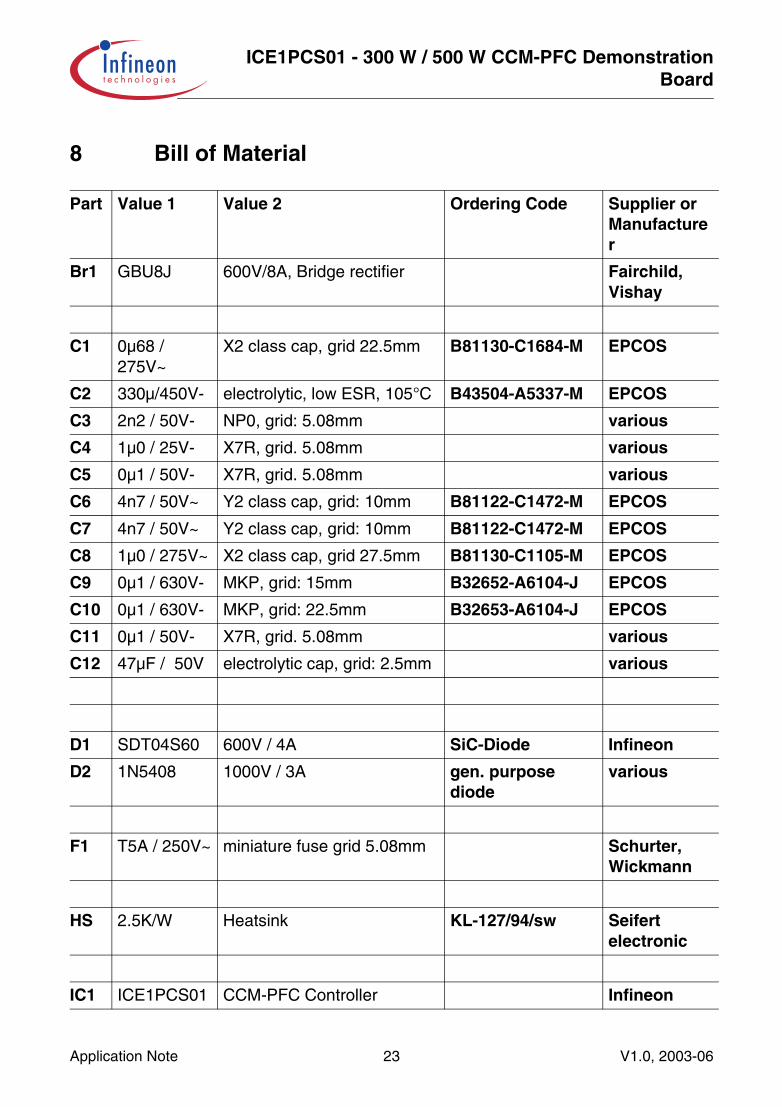
8 Bill of Material
Part Value 1 Value 2 Ordering Code Supplier or Manufacturer
Br1 GBU8J 600V/8A, Bridge rectifier Fairchild, Vishay
C1 0µ68 / 275V~
X2 class cap, grid 22.5mm B81130-C1684-M EPCOS
C2 330µ/450V- electrolytic, low ESR, 105°C B43504-A5337-M EPCOS
C3 2n2 / 50V- NP0, grid: 5.08mm various
C4 1µ0 / 25V- X7R, grid. 5.08mm various
C5 0µ1 / 50V- X7R, grid. 5.08mm various
C6 4n7 / 50V~ Y2 class cap, grid: 10mm B81122-C1472-M EPCOS
C7 4n7 / 50V~ Y2 class cap, grid: 10mm B81122-C1472-M EPCOS
C8 1µ0 / 275V~ X2 class cap, grid 27.5mm B81130-C1105-M EPCOS
C9 0µ1 / 630V- MKP, grid: 15mm B32652-A6104-J EPCOS
C10 0µ1 / 630V- MKP, grid: 22.5mm B32653-A6104-J EPCOS
C11 0µ1 / 50V- X7R, grid. 5.08mm various
C12 47µF / 50V electrolytic cap, grid: 2.5mm various
D1 SDT04S60 600V / 4A SiC-Diode Infineon
D2 1N5408 1000V / 3A gen. purpose diode
various
F1 T5A / 250V~ miniature fuse grid 5.08mm Schurter, Wickmann
HS 2.5K/W Heatsink KL-127/94/sw Seifert electronic
IC1 ICE1PCS01 CCM-PFC Controller Infineon
Application Note 23 V1.0, 2003-06

ICE1PCS01 - 300 W / 500 W CCM-PFC DemonstrationBoard
L1 350µH/ 4,3A PFC choke 169340 Lasslop
L2 2x3,9mH/6A EMI ferrite choke B82725-J2602-N20 EPCOS
L3 2,2 mH EMI ferrite choke 169800 Lasslop
R1 0R1 5W, low-L, grid: 9mm MPC71 series Fukushima Futaba
R2 220R 0,4W, 2%, grid: 10.08 metal film various
R3A 220k 0,4W, 2%, grid: 10.08 metal film various
R3B 220k 0,4W, 2%, grid: 10.08 metal film various
R4 5k6 0,4W, 2%, grid: 10.08 metal film various
R5 33k 0,4W, 2%, grid: 10.08 metal film various
R6 10k 0,4W, 2%, grid: 10.08 metal film various
R7 15R 0,4W, 2%, grid: 10.08 metal film various
R8 12k 0,4W, 2%, grid: 10.08 metal film various
R9 1k0 0,4W, 2%, grid: 10.08 metal film various
R10 1k0 0,4W, 2%, grid: 10.08 metal film various
T1 SPP21N50 500V / 20A Q67040S4585 Infineon
T2 BC237 45V, 350mW, npn-transistor general purpose various
X1 connector 3 terminal: 480V, 15A, RM5 AST02 5 03 04 RIA
X2 connector 3 terminal: 480V, 15A, RM5 AST02 5 03 04 RIA
X3 connector 2 terminal: 480V, 15A, RM5 AST02 5 02 04 RIA
Part Value 1 Value 2 Ordering Code Supplier or Manufacturer
Application Note 24 V1.0, 2003-06

ICE1PCS01 - 300 W / 500 W CCM-PFC DemonstrationBoard
9 Summary of Used NomenclaturePhysics
General identifiers: Special identifiers:
A .........cross areab, B .....magnetic inductancec, C .....capacitanced, D .....duty cyclef...........frequencyi, I ........currentl, L .......inductianceN .........number of turnsp, P .....powert, T.......time, time-intervalsv, V......voltageW ........energyh..........efficiency
K1, K2 ..ferrite core constants
AL........... inductance factorV(BR)CES .. collector-emitter breakdown
voltage of IGBTVF........... forward voltage of diodesVrrm .......... maximum reverse voltage of diodes
big letters: constant values and time intervals
small letters: time variant values
Components:
C .........capacitorD .........diodeIC ........integrated circuitL..........inductorR .........resistorTR.......transformer
Indices:
AC.......alternating current valueDC.......direct current valueBE.......basis-emitter valueCS.......current sense valueOPTO..optocoupler valueP .........primary side valuePk........peak valueR........... reflected from secondary to primary sideS .........secondary side valueSh .......shunt valueUVLO..undervoltage lockout valueZ..........zener value
fmin ......... value at minimum pulse frequencyi ..............running variablein ............input valuemax ........maximum valuemin .........minimum valueoff ...........turn-off valueon ...........turn-on valueout ..........output valuep .............pulsedrip ...........ripple value
1, 2, 3 .....on-going designator
Application Note 25 V1.0, 2003-06

ICE1PCS01 - 300 W / 500 W CCM-PFC DemonstrationBoard
10 References
[1] Infineon Technologies: ICE1PCS01 - Standalone Power Factor CorrectionController in Continuous Conduction Mode; Preliminary datasheet; InfineonTechnologies; Munich; Germany;
[2] W. Frank: ICE1PCS01 - Getting Started; Application Note AN-PFC-ICE1PCS01-2; Infineon Technologies; Munich; Germany; 02/03.
[3] B. Ilchmann: 6W Bias Supply for SMPS with ICE2A0565Z; Application Note AN-CoolBIAS; Infineon Technologies; Munich; Germany; 09/02
Application Note 26 V1.0, 2003-06

w w w . i n f i n e o n . c o m
Published by Infineon Technologies AG
Inf ineon goes for Business Excel lence
“Business excellence means intelligent approaches and clearlydefined processes, which are both constantly under review andultimately lead to good operating results.
Better operating results and business excellence mean lessidleness and wastefulness for all of us, more professionalsuccess, more accurate information, a better overview and,thereby, less frustration and more satisfaction.”
Dr. Ulrich Schumacher


